Embed Size (px)
Citation preview

• Light Emitting Diode (LED)- Structure, Material, Quantum efficiency, LED Power
• Laser Diodes (LD)- Structure, Modes, Rate equation, Quantum efficiency,
Resonant frequencies, Radiation pattern
Semiconductor light sources

Basov, Prokhorov and Townes: Nobel prize 1964
Basov, Vul, Popov, Krokhin: 1957 first semiconductor laser proposal and development1961 first injection laser proposal (also Dumke 1962)
“for fundamental work in the field of quantum electronics, which has led to the construction of oscillators and amplifiers based on the maser-laser principle"

Zhores I. Alferov Herbert Kroemer
The Nobel Prize in Physics 2000
"for developing semiconductor heterostructures used in high-speed- and opto-electronics"

Light-Emitting Diodes (LEDs)
• For photonic communications requiring data rate 100-200 Mb/s with multimode fiber with tens of microwatts, LEDs are usually the best choice.
• LED configurations being used in photonic communications:1- Surface Emitters (Front Emitters)2- Edge Emitters

Homojunction

Forward biased junction

Ec
Ev
Eg1 Eg2
Type I
Ec
EvEg1
Eg2
Ec
Ev
Type II
Type III
Eg1
Eg2Ev
Ec
Heterojunctions

Double Heterojunction
Wide-gap semiconductor
Narrow-gap semiconductor
Wide-gap semiconductor
zEg2
Eg2
Eg1
Eg2 Eg1
z
Valence band edge
Conduction band edge

Cross-section drawing of a typical GaAlAs double heterostructure light emitter. In this structure, x>y to provide for both carrier confinement and optical guiding. b) Energy-band diagram showing the active region, the electron & hole barriers which confine the charge carriers to the active layer. c) Variations in the refractive index; the lower refractive index of the material in regions 1 and 5 creates an optical barrier around the waveguide because of the higher band-gap energy of this material.
)eV(240.1m)(
gE [4-3]

Surface-Emitting LED
Schematic of high-radiance surface-emitting LED. The active region is limitted to a circular cross section that has an area compatible with the fiber-core end face.

Edge-Emitting LED
Schematic of an edge-emitting double heterojunction LED. The output beam is lambertian in the plane of junction and highly directional perpendicular to pn junction. They have high quantum efficiency & fast response.

Light Source Material• Most of the light sources contain
III-V ternary & quaternary compounds.
• by varying x emission wavelength over the range of 800 nm to 900 nm. The spectral width is 20 to 40 nm.
• By changing 0<x<0.47; y is approximately 2.2x, the emission wavelength of 920 nm to 1600 nm. The spectral width varies from 70 nm to 180 nm when the wavelength changes from 1300 nm to 1600 nm. These materials are lattice matched.
AsAlGa xx1
y1yxx1 PAsGaIn

Spectral width of LED types

Rate equations, Quantum Efficiency & Power of LEDs
• When there is no external carrier injection, the excess density decays exponentially due to electron-hole recombination.
• n is the excess carrier density,
• Bulk recombination rate R:
• Bulk recombination rate (R) = Radiative recombination rate + nonradiative recombination rate
/0)( tentn
lifetime.carrier :densityelectron excess injected initial :0
n
n
dtdnR
)1rate(ion recombinat venonradiati )1( rateion recombinat radiative)1( rateion recombinatbulk
r nrnrr /τR/τR/τR
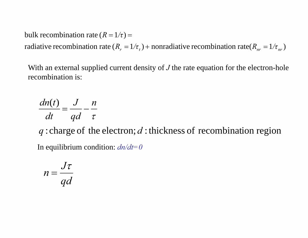
With an external supplied current density of J the rate equation for the electron-hole recombination is:
regionion recombinat of thickness: electron; theof charge :
)(
dq
nqdJ
dttdn
In equilibrium condition: dn/dt=0
qdJn
rnrr
nr
nrr
r
RRR
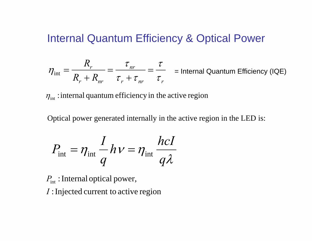
int
Internal Quantum Efficiency & Optical Power
region active in the efficiency quantum internal :int
Optical power generated internally in the active region in the LED is:
qhcIh
qIP intintint
region active current to Injected :power, optical Internal :int
IP
= Internal Quantum Efficiency (IQE)

External Quantum Eficiency
• In order to calculate the external quantum efficiency, we need to consider the reflection effects at the surface of the LED. If we consider the LED structure as a simple 2D slab waveguide, only light falling within a cone defined by critical angle will be emitted from an LED.
photons generated internally LED of #LED from emitted photons of #
ext

dTc
)sin2()(41
0ext
221
21
)(4)0(tCoefficienon Transmissi Fresnel :)(
nnnnTT
211
ext2 )1(11 If
nn
n
intext int 2
1 1
LED emitted optical power, ( 1)
PP Pn n

Laser Diodes (LDs)

1. Active (gain) medium that can amplify light that passes through it
2. Energy pump source to create a population inversion in the gain medium
3. Two mirrors that form a resonator cavity
Reminder: LASER (Light Amplification by the Stimulated Emission of Radiation)

LASER (Light Amplification by the Stimulated Emission of Radiation)
• Laser is an optical oscillator. It comprises a resonant optical amplifier whose output is fed back into its input with matching phase. Any oscillator contains:1- An amplifier = pumped active medium2- A feedback system = optical resonantor3- A frequency selection mechanism (both of the above)4- An output coupling scheme (one of the resonator mirrors)
No (or negative) feedback:
Positive feedback:

Lasing in a pumped active medium
• In thermal equilibrium the stimulated emission is essentially negligible, since the density of electrons in the excited state is very small, and optical emission is mainly because of the spontaneous emission. Stimulated emission will exceed absorption only if the population of the excited states is greater than that of the ground state. This condition is known as Population Inversion. Population inversion is achieved by various pumping techniques.
• In a semiconductor laser, population inversion is accomplished by injecting electrons into the material to fill the lower energy states of the conduction band.

Refractiveindex
Photondensity
Activeregion
n ~ 5%
2 eV
Holes in VB
Electrons in CB
AlGaAsAlGaAs
1.4 eV
Ec
Ev
Ec
Ev
(a)
(b)
pn p
Ec
(a) A doubleheterostructure diode hastwo junctions which arebetween two differentbandgap semiconductors(GaAs and AlGaAs).
2 eV
(b) Simplified energyband diagram under alarge forward bias.Lasing recombinationtakes place in the p-GaAs layer, theactive layer
(~0.1 m)
(c) Higher bandgapmaterials have alower refractiveindex
(d) AlGaAs layersprovide lateral opticalconfinement.
(c)
(d)
© 1999 S.O. Kasap, Optoelectronics (Prentice Hall)
GaAs
Carrier confinement and optical guiding in a laser diode
)eV(240.1m)(
gE

Laser Diode• Laser diode is a vastly improved LED, in the sense that uses stimulated
emission in semiconductor from optical transitions between energy states of the valence and conduction bands with optical resonator structure such as Fabry-Perot resonator with both optical and carrier confinements.

Fabry-Perot Resonator

Fabry-Perot ResonatorA
BL
M1 M2 m = 1
m = 2
m = 8
Relative intensity
m
m m + 1m - 1
(a) (b) (c)
R ~ 0.4R ~ 0.81 f
Schematic illustration of the Fabry-Perot optical cavity and its properties. (a) Reflectedwaves interfere. (b) Only standing EM waves, modes, of certain wavelengths are allowedin the cavity. (c) Intensity vs. frequency for various modes. R is mirror reflectance andlower R means higher loss from the cavity.
© 1999 S.O. Kasap, Optoelectronics (Prentice Hall)
)(sin4)1()1(
22
2
kLRRRII inctrans
R: reflectance of the optical intensity, k: optical wavenumber
1,2,3,.. :modesResonant mmkL

Comparison between an LD and LED
• Laser Diode– Stimulated radiation– narrow linewidth– coherent– higher output power– a threshold device– strong temperature
dependence– higher coupling
efficiency to a fiber
• LED– Spontaneous radiation– broad spectral– incoherent– lower output power– no threshold current– weak temperature
dependence– lower coupling
efficiency

Laser Diode Characteristics
• Nanosecond & even picosecond response time (GHz BW)• Spectral width of the order of nm or less• High output power (>tens of mW)• Narrow beam (good coupling to single mode fibers)
• Laser diodes have three distinct radiation modes namely, longitudinal, lateral and transverse modes.
• In laser diodes, end mirrors provide strong optical feedback in longitudinal direction, so by roughening the edges and cleaving the facets, the radiation can be achieved in longitudinal direction rather than lateral direction.

Laser Operation & Lasing Condition• To determine the lasing condition and resonant frequencies, we
should focus on the optical wave propagation along the longitudinal direction, z-axis. The optical field intensity, I, can be written as:
• Lasing is the condition at which light amplification becomes possible by virtue of population inversion. Then, stimulated emission rate into a given EM mode is proportional to the intensity of the optical radiation in that mode. In this case, the loss and gain of the optical field in the optical path determine the lasing condition. The radiation intensity of a photon at energy varies exponentially with a distance z amplified by factor g, and attenuated by factor according to the following relationship:
)()(),( ztjezItzI
h

( ) (0)exp ( ) ( )iI z I g h h z
1R 2R
Z=0 Z=L
1 2(2 ) (0) exp ( ) ( ) (2 )iI L I R R g h h L
2
1 2
1 2
: Optical confinement factor, g: gain coefficient: effective absorption coefficient, iα
n nRn n
1n
2n
Lasing Conditions:1)2exp(
)0()2(
Lj
ILI

Threshold gain & current density
1 2
1 1ln2th i m ig
L R R
Laser starts to "lase" if: thg g
For laser structure with strong carrier confinement, the threshold current Density for stimulated emission can be well approximated by:

Optical output vs. drive current
Typical output optical power vs. diode current ( I) characteristics and the correspondingoutput spectrum of a laser diode.
Laser
LaserOptical P ower
Optical P ower
I0
LEDOptical P ower
It h
Spontaneousemission
Stimulatedemission
Optical Power
© 1999 S.O. Kasap, Optoelectronics (Prentice Hall)

Semiconductor laser rate equations• Rate equations relate the optical output power, or # of photons per unit
volume, , to the diode drive current or # of injected electrons per unit volume, n. For active (carrier confinement) region of depth d, the rate equations are:
emission stimulatedionrecombinat sspontaneouinjectionrateelectron
lossphoton emission sspontaneouemission stimulatedratePhoton
CnnqdJ
dtdn
RCndtd
sp
phsp
densitycurrent Injection
timelifephoton
mode lasing theintoemission sspontaneou of rate
process absorption &emission optical theofintensity theexpressingt Coefficien
:
:
: :
J
RC
ph
sp

Threshold current Density & excess electron density
• At the threshold of lasing:
• The threshold current needed to maintain a steady state threshold concentration of the excess electron, is found from electron rate equation under steady state condition dn/dt=0 when the laser is just about to lase:
0 ,0/ ,0 spRdtd
1 / 0ph thph
Cn n nC
sp
thth
sp
thth nqdJnqdJ
0

Laser operation beyond the threshold
• The solution of the rate equations gives the steady state photon density, resulting from stimulated emission and spontaneous emission as follows:
thJJ
spphthph
s RJJqd
)(

External (differential) quantum efficiency
• Number of photons emitted per radiative electron-hole pair recombination above threshold, gives us the external quantum efficiency.
ext (photon energy) x(photon density) x(effective volume of the optical mode) x(escape rate of photons)
( )( )
( )
//
out s op g m
mout i th
i m
outext
P wLd v
P I Iq
dP dIq
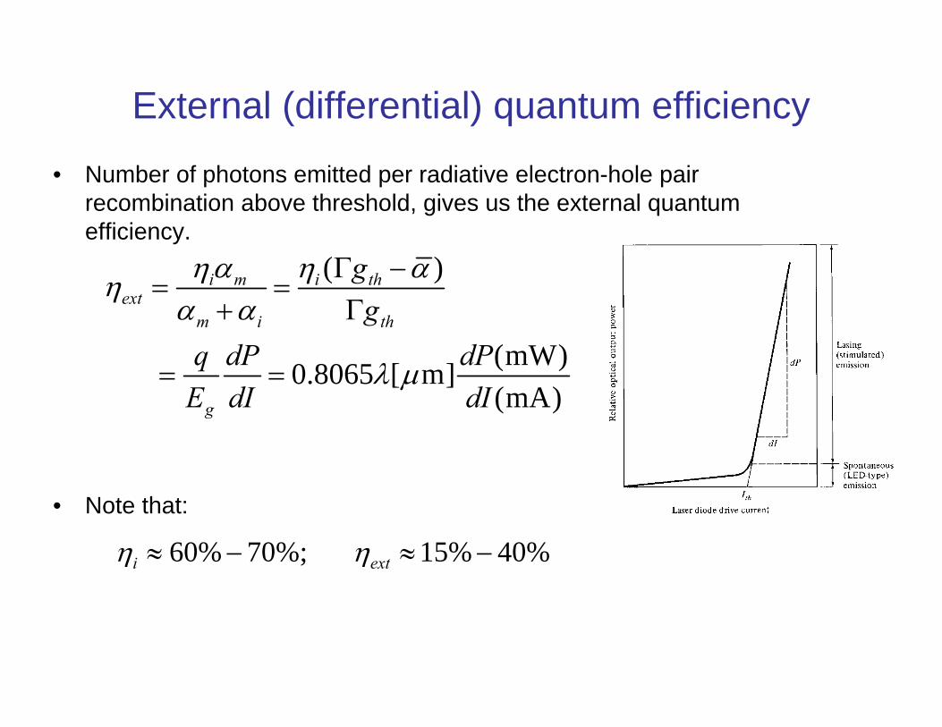
External (differential) quantum efficiency
• Number of photons emitted per radiative electron-hole pair recombination above threshold, gives us the external quantum efficiency.
• Note that:
( )
(mW) 0.8065 [ m](mA)
i m i thext
m i th
g
gg
q dP dPE dI dI
%40%15 %;70%60 exti

Emission Spectra of the typical DH laser
• Emission spectra of a perfect laser– above the threshold, the laser may
approach near-perfect monochromatic emission with a spectra width in the order of 1 to 10 Å.
• High-resolution emission spectra(of a typical stripe-geometry DH laser)
– Sub-peaks, which are evenly spaced with a separation of = 7.5 Å, appear in the spectra. belong to the longitudinal modes.
– Because of these longitudinal modes, the stripe geometry laser is not a spectrally pure light source for optical communication.

Laser Resonant Frequencies• Lasing condition:
• Assuming the resonant frequency of the mthmode is:
,...3,2,1 ,2L2 1)2exp( mmLj
n2
1,2,3,... 2
mLn
mcm
LnLnc
mm 22
2
1
n = refractive index

Spectrum from a laser Diode
widthspectral: 2
)(exp)0()( 20
gg

Characteristics of the DH laser
Threshold current density vs. active layer thickness
– The threshold current density decreases with decreasing d, reaches a minimum, and then increases. The increase of Jth at very narrow active thickness is caused by poor optical confinement.
Output power vs. diode current– The light-current characteristics is
quite linear above threshold.
Temperature dependence– The threshold current increases
exponentially with temperature Jth ~ exp [ T/T0 ]

Design considerations for laser diode performance
• Low threshold current– low threshold can be generated by electronic devices which can be
modulated at high speed to provide a high speed modulation in the output(1) reducing the active layer thickness (d)
↣ Quantum-Well (~ 50 - 100 Å), Strain Quantum-Well (2) N-doped active region (3) Stripe geometry
• Lateral confinement– to avoid the “kink” effect, which produces noise in the optical transmitter reduce the lateral dimension of the Fabry-Perot cavity (1) Stripe geometry (Gain-guided cavity)
(2) Buried heterostructures
• Selective Optical Cavity– to reduce the laser linewidth (1) Distributed Feedback (DFB) structures
(2) Vertical Cavity Surface Emitting Lasers (VCSELs)