Embed Size (px)
Citation preview
Organic Covalent Patterning of Nanostructured Graphene withSelectivity at the Atomic LevelJuan Jesus Navarro,† Sofía Leret,† Fabian Calleja,† Daniele Stradi,†,‡ Andres Black,†,§
Ramon Bernardo-Gavito,†,§ Manuela Garnica,†,§ Daniel Granados,† Amadeo L. Vazquez de Parga,*,†,§
Emilio M. Perez,*,† and Rodolfo Miranda†,§
†IMDEA Nanociencia, Calle Faraday 9, Cantoblanco 28049, Madrid, Spain‡Departamento de Química, Modulo 13 and §Departamento de Física de la Materia Condensada and IFIMAC, UniversidadAutonoma de Madrid, Cantoblanco 28049, Madrid, Spain
*S Supporting Information
ABSTRACT: Organic covalent functionalization of graphenewith long-range periodicity is highly desirableit is anticipatedto provide control over its electronic, optical, or magneticpropertiesand remarkably challenging. In this work wedescribe a method for the covalent modification of graphenewith strict spatial periodicity at the nanometer scale. The periodic landscape is provided by a single monolayer of graphene grownon Ru(0001) that presents a moire pattern due to the mismatch between the carbon and ruthenium hexagonal lattices. Themoire contains periodically arranged areas where the graphene−ruthenium interaction is enhanced and shows higher chemicalreactivity. This phenomenon is demonstrated by the attachment of cyanomethyl radicals (CH2CN
•) produced by homolyticbreaking of acetonitrile (CH3CN), which is shown to present a nearly complete selectivity (>98%) binding covalently tographene on specific atomic sites. This method can be extended to other organic nitriles, paving the way for the attachment offunctional molecules.
KEYWORDS: Nanostructured graphene, epitaxial graphene, chemical functionalization, scanning tunneling microscopy
Graphene is a bidimensional network of sp2-hybridizedcarbon atoms. The planar hexagonal arrangement of
carbon in graphene, its chemical stability, and mostsignificantly, its extraordinary physical properties all stemfrom the extended conjugation provided by the homogeneoussp2 hybridization.1 The chemical functionalization of graphenehas been intensely pursued in the last years.2,3 A significant partof the research efforts from the wet chemistry trench havefocused on the covalent attachment of molecular fragments tographene. The addition of malonate-type carbanions andradicals, acylations, and a wide variety of cycloadditions,including [2 + 1], [2 + 2], [3 + 2], and [4 + 2], have allbeen explored, among others.4−7 Negative consequences ofgraphene’s planar geometry are its insolubility and its tendencyto reaggregate to form graphite through π−π and van der Waalsinteractions. Such issues can be solved using graphene on asuitable substrate (for a recent review see Criado et al.8). It hasbeen demonstrated that graphene grown or deposited on asubstrate can physisorb or chemisorb molecules. Weaklyattached adsorbates can act as donors or acceptors leading tochanges in carrier concentration that allow the detection ofsingle molecules9 or the formation of intermolecular bands withlong-range magnetic order at low temperatures.10 Beyond thesupramolecular functionalization of epitaxial graphene, itscovalent modification has been proposed as an ideal tool foradjusting the electronic, optical, or magnetic properties. Thechemical oxidation of graphene in ultrahigh vacuum (UHV)
conditions has also been demonstrated.11,12 The attachment ofhydrogen to each atomic site of the graphene lattice to creategraphane was proposed,13 resulting in a change in thehybridization of carbon atoms from sp2 to sp3, as well as theopening of a sizable gap at the Dirac point.14−16 In theseexperiments, all of the atoms in the graphene lattice exhibit verysimilar reactivity, and the only way to get an atomically well-defined long-range order is to saturate all the atomic sites,creating a completely new material, e.g., graphane or grapheneoxide. This lack of selectivity is a major drawback if theobjective of the covalent modification is to modulate theelectronic properties of graphene. It has been predicted that aperiodic patterning of graphene would lead to new electronicproperties17 including a direct relation between the periodicityand the bandgap amplitude.18,19 Therefore, the chemicalfunctionalization of graphene in a periodic fashion with aperiodicity in the range of 1−5 nm is highly desirable.There have been several approaches for obtaining site
selectivity in the chemical functionalization of graphene. Oneapproach relies on patterning the surface using an atomic forcemicroscope (AFM).20,21 The main drawback of this approach isthe time needed to write the motifs and also the difficulty ofscaling up the process to millimeter size samples. Another
Received: September 28, 2015Revised: November 30, 2015
Letter
pubs.acs.org/NanoLett
© XXXX American Chemical Society A DOI: 10.1021/acs.nanolett.5b03928Nano Lett. XXXX, XXX, XXX−XXX
approach relies on the fact that strain and curvature stronglyenhance the local reactivity of graphene,22,23 although so far nolong-range order has been achieved. Graphene grown onmetallic substrates presents a moire pattern due to thedifference in lattice parameter between graphene and thesubstrate.24 In particular, graphene grown on Ir(111) has beenused to study the influence of a spatially ordered covalentfunctionalization in the graphene electronic structure.25,26 Dueto the weak interaction between the graphene and the Ir(111)substrate, the moire pattern presents several rotational domainswith different periodicities.27,28 The weak interaction with thesubstrate also renders all of the carbon atoms almost identicalelectronically, and no distinct reactive sites are present in thesystem. To the best of our knowledge, there have been noreports of covalent functionalization of graphene with atomic-level selectivity.Here, we describe a method for the organic covalent
modification of graphene with exquisite spatial periodicity atthe atomic scale. We take advantage of the fact that the growthof graphene on lattice-mismatched metallic substrates allows usto tailor the geometric and electronic properties of thegraphene overlayer in a periodic fashion. In particular, we usegraphene grown on Ru(0001) that presents a moire patternwith a periodicity of ≈3 nm. The moire shows periodicallydistributed areas where the charge transfer due to theinteraction between graphene and ruthenium is rather large
and, as a consequence, these graphene areas present higherchemical reactivity. This point is illustrated by demonstratingthat cyanomethyl radicals (CH2CN
•) produced by homolyticbreaking of acetonitrile (CH3CN) in UHV by electronbombardment bind to graphene preferentially at specific atomicsites with a nearly complete selectivity (>98%).Growth of graphene through chemical vapor deposition
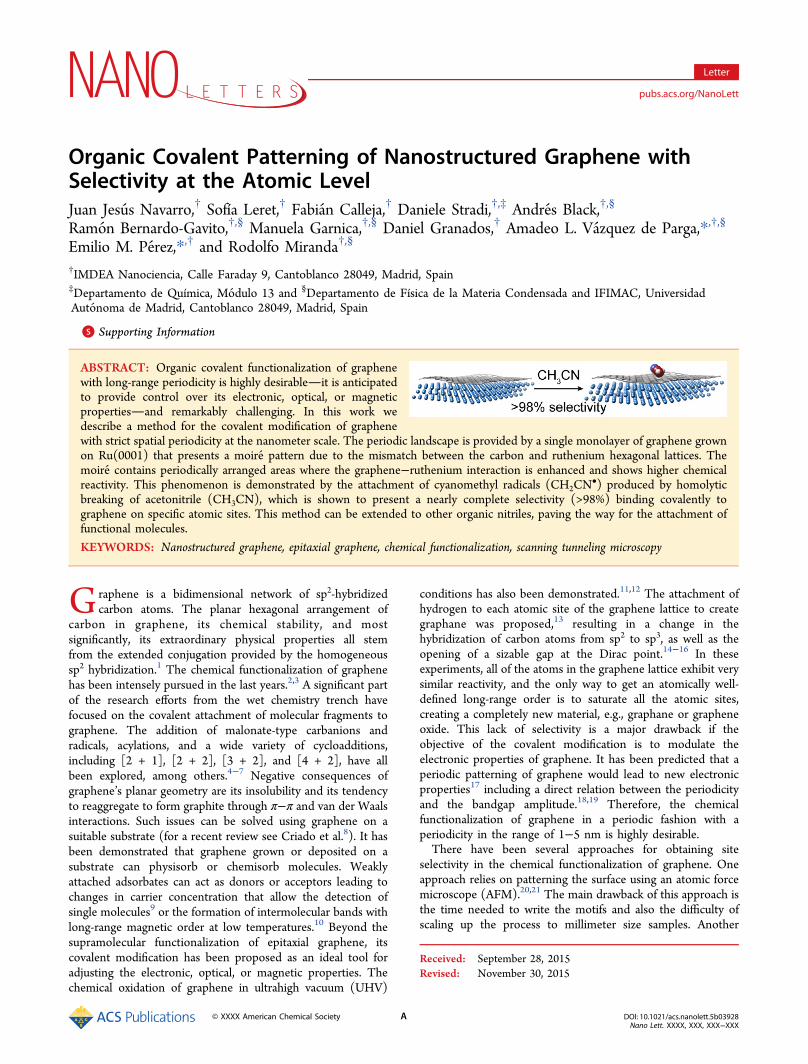
(CVD) on a variety of metallic substrates is one of thepreferred methods for the synthesis of high-quality gra-phene.29−32 This method presents the additional advantagethat the strength of the interaction between graphene and themetallic substrate can be tuned by varying the chemical natureof the latter.33 In this respect, some of us have previouslyreported the epitaxial growth of graphene on Ru(0001)(hereafter, gr/Ru(0001)) where due to the mismatch betweenthe hexagonal lattices of graphene and Ru, the system presentsa moire pattern with a surface periodicity of 2.93 nm34 (seeSupporting Information A for further details). Figure 1a showsthat three different areas can be distinguished inside the moire unit cell depending on the registry between the carbon atomsand the last two ruthenium atomic layers, namely, the “atop”region where all carbon atoms are placed above 3-fold hollowsites of the Ru surface (vertex of the blue triangles in Figure1a), the “HCP-Top” region where half of the carbon atoms arelocated on HCP 3-fold positions and the other half on top ofRu atoms (dashed blue triangle in Figure 1a) and the “FCC-
Figure 1. (a) Model of the gr/Ru(0001) surface, where gray circles represent the Ru atoms of the first atomic layer. The graphene hexagonal latticeis shown in a black to white color scale to indicate the height of the carbon atoms respect to the Ru(0001) surface. The unit cell of the moire patternis highlighted by two blue triangles. At the vertices all carbon atoms fall on 3-fold hollow sites of the Ru(0001) surface. At the center of the solid(dashed) triangle one carbon sublattice falls on FCC-stacked (HCP-stacked) 3-fold hollow sites and the other one on top positions. These tworegions are named “FCC-Top” and “HCP-Top” respectively. (b) STM image acquired on pristine gr/Ru(0001) (24 × 7 nm2; Vb = +1.5 V, It = 30pA). The moire pattern arising from the lattice mismatch is highlighted in blue. The HCP-Top area is marked with the dashed triangle, and the FCC-Top area is marked the solid triangle. Four point defects on the atop areas are indicated by black circles.
Nano Letters Letter
DOI: 10.1021/acs.nanolett.5b03928Nano Lett. XXXX, XXX, XXX−XXX
B

Top” region where half of the carbon atoms are located onFCC 3-fold positions and the other half on top of Ru atoms(solid blue triangle in Figure 1a).Figure 1b shows a scanning tunneling microscope (STM)
topographic image of the surface measured at +1.5 V biasvoltage. Under these bias conditions, the moire appears as ahexagonal array of bumps with a small corrugation (∼40 pm).The origin of the bumps is the change in registry within themoire unit cell that produces a spatial modulation in theinteraction between the C and Ru atoms, from weak van derWaals interaction in the high areas of the STM images to stronginteraction in the lower areas.35,36 This spatial variation of theinteraction modulates all surface electronic properties, from thesurface potential37 to the electronic structure around the Fermilevel,34 which directly affects the chemical reactivity. The STMimaging conditions of Figure 1b also reveal the presence of fourpoint defects on top of the ripples (marked with black circles),
which we attribute to subsurface oxygen trapped during thegraphene growth process (see Supporting Information B fordetails).Recently, Ruoff, Bielawsky, and co-workers have introduced a
method for the selective functionalization of graphene on areaswith high local curvature.22 Considering this, and the seminalwork by Balog et al. on the patterned hydrogenation ofgraphene on Ir,25 we reasoned that graphene on Ru(0001)seems an ideal playground to exploit a similar strategy for aperiodic chemical modification of graphene with subnanoscaleselectivity. The metal−graphene interaction in gr/Ru(0001) issufficiently strong to affect the chemical reactivity of specificatomic sites of the graphene overlayer, due to the presence ofthe moire-related corrugation. While attempting to reproducethe wet-chemistry reaction conditions, we serendipitouslydiscovered that gr/Ru(0001) can be functionalized bycyanomethyl radicals with exquisite spatial selectivity (see
Figure 2. (a−f) 10 × 10 nm2 STM images with different bias voltages acquired at 80 K after exposing gr/Ru(0001) to 180 Langmuir of acetonitrileat 300 K. Notice the related presence of seven bright bumps on HCP-Top sites (marked with a white circle), one on FCC-Top site and onegraphene point defect (marked with a black circle). (g) Differential conductance, dI/dV, curves recorded at 80 K with the tip of the STM placed ontop of the molecular attachments (green), the FCC-Top, HCP-Top (purple and blue, respectively), and the ripples (black) areas of the moire pattern of gr/Ru(0001). The dI/dV individual curves were measured in open feedback loop conditions with the tunneling gap stabilized at +0.3 Vand 50 pA. The lock-in signal was acquired using a modulation in the bias voltage of 40 mV (rms), a frequency of 856 Hz, and a time constant of 10ms.
Nano Letters Letter
DOI: 10.1021/acs.nanolett.5b03928Nano Lett. XXXX, XXX, XXX−XXX
C

Supporting Information C for details). Representative STMimages are shown in Figure 2a−f, measured at 80 K as afunction of the sample bias voltage after exposure of the sampleat room temperature to 1 × 10⁻⁶ Torr of CH3CN for 3 min,equivalent to 180 Langmuirs. Bright bumps related to theadsorption of acetonitrile, located exclusively at the valleys andthe HCP-top sites, are observed for voltages between +1.25 Vand +2 V. The molecular attachments show an apparent heightof 26 ± 2 pm and a lateral width of 560 ± 20 pm at +1.5 V. Theshape and size of the molecular attachments are very similar tothose measured on STM images taken of acetonitrile adsorbedon Pt(111).38 Figure 2g shows scanning tunnelling spectros-copy (STS) recorded on various positions of the moire unitcell. The curves measured on top of the ripples, and the onesmeasured on the (empty) low areas of the moire show the well-known asymmetry between the occupied and empty density ofstates of gr/Ru(0001).34 The curves measured on the molecularattachments present an additional peak at +1.6 eV identified asthe lowest unoccupied molecular orbital (LUMO). The energyof the highest occupied molecular orbital (HOMO) is below−2.0 V and, therefore, out of the measured energy window.The images confirm that for bias voltages below +0.5 V themolecular attachments are not visible, since tunneling is beingcarried out in the gap between the HOMO and LUMO. Forbias voltages larger than +2.5 V the reduction in the apparentcorrugation of the moire pattern and its subsequent inversion39
hinders the precise identification of the adsorption site of themolecular attachments.Remarkably, single molecular attachments can be observed
exclusively at the valleys of the moire pattern. Moreover, thereis a strong preference for HCP-Top sites over FCC-top regionsoffering another level of selectivity. For higher coverages on theorder of 0.50 acetonitrile molecules per moire unit cell, 98 ±1% of the HCP-Top and 2 ± 1% of the FCC-Top areas of theunit cells are occupied. The same site preference has beenobserved for TCNQ40 and F4-TCNQ
41 molecules adsorbed ongr/Ru(0001) and can be understood considering the differencein the electronic structure between the FCC-Top and HCP-Top areas.40
In the present case, however, the bonding between theadsorbed molecular attachments and graphene relies on astrong C−C covalent bond, which modifies the sp2 hybrid-ization of a single C atom in graphene. This is demonstrated inFigure 3, in which a region containing three molecularattachments located in HCP-Top regions, encircled in white,is imaged with atomic resolution. The STM image has beentaken in conditions where the molecular attachment istransparent (2 mV bias and 800 pA current) because thesmall bias voltage is probing the energy gap between HOMOand LUMO of the adsorbed molecule. Accordingly, the tip doesnot move up when it is located on top of the moleculesattached to the surface. Simultaneously, the C atoms with amodified hybridization where the three molecules are bondedappear as single atom “holes” (see Supporting Information F3and Figure S7 for details). Remarkably, the covalent attach-ments are located exclusively on crystallographically identicalcarbon atoms of the graphene overlayer. The inset shows thebright bumps of the molecules adsorbed on the “hole” sites byrestoring a bias voltage where they can be imaged through theirLUMO orbitals. In spite of the harsh imaging conditions allthree molecules remain in place, without any noticeable changein shape or position. Going down to atomic resolutionparameters without sweeping the molecular attachments awayduring the scan is contrary to what happens with physisorbedor even strongly chemisorbed isolated molecules, such asTCNQ9 or F4-TCNQ,
42 indicating the covalent nature of theirattachment to graphene. In fact, the molecular attachmentscannot be displaced from their adsorption sites by the STM tipfollowing standard manipulation techniques.43,44 Annealing thesample in UHV further confirms the strong bond betweengraphene and the molecular attachments. The sample remainsunaltered up to 573 K.These facts confirm the selective covalent patterning of gr/
Ru(0001) through treatment with CH3CN beyond reasonabledoubt. Given the relatively inert nature of CH3CN, andknowing that under high-vacuum (10−6 Torr) conditions iongauges produce and emit active chemical species throughionization of the residual gases in the vacuum chamber, whichcan be adsorbed onto graphene,45 we reasoned the same
Figure 3. High resolution STM image (17 × 12 nm2, Vb = 2 mV, It = 800 pA), acquired at 80 K on a region containing three molecular attachments(white circles) and two oxygen-related defects on graphene (black circles). Inset: Same region scanned afterward with Vb = +1.7 V and It = 100 pA.All three molecular attachments are still in place. The moire unit cell is highlighted in blue in the inset.
Nano Letters Letter
DOI: 10.1021/acs.nanolett.5b03928Nano Lett. XXXX, XXX, XXX−XXX
D

process may take place during the exposure of the graphenesurface to the acetonitrile molecules in UHV, since we use anion gauge to measure the partial pressure of the acetonitrile gas.In order to gather experimental evidence of the molecularfragments that can be produced in the ion gauge during theCH3CN exposition, we introduced in the UHV chamber thesame partial pressure (1 × 10⁻⁶ Torr) of acetonitrile usedduring the graphene exposure and recorded the mass spectrumof the gas utilizing a quadrupole mass spectrometer (QMS)(see Supporting Information D for details). The ionizationchamber of the QMS works under the same physical principleas the ion gauges and therefore the spectra measured is areliable indicator of the chemical species produced in the iongauge. The m/z pattern is perfectly consistent with a significantconcentration of CH2CN
• (Figure S3 and SupportingInformation D for details). It is well-known that CH2CN
•
can be generated directly from CH3CN by homolytic cleavageof a C−H bond.46−48 Moreover, the cyanomethyl radical(CH2CN
•) is known to react with C−C double bonds49−51 andarenes52 forming C−C bonds.To provide further experimental evidence for this hypothesis,
we exposed the sample to 180 Langmuir of acetonitrile with theion gauge in the preparation chamber turned of f, and underthese conditions no molecular attachments were detected onthe surface (see Supporting Information G for further details).To gain atomic understanding of the reaction, we ran DFT
calculations for the adsorption of CH2CN• on gr/Ru(0001).
The results are summarized in Figure 4. In agreement with theexperimental data, the adsorption energies are within the limitsof a covalent bond (>2.1 eV) (see Figure 4a). Remarkably, theHCP-Top/FCC-Top preference we observe experimentally isalso reproduced. The two most stable configurations, HCP-Top(1) and HCP-Top(4), with adsorption energies of 2.34 and2.49 eV are shown in Figure 4b and c. In this case, it is the alkylcarbon atom of CH2CN
• that lies closer to the graphenesurface, as is observed in the cycanomethylation of arenes.52
The graphene carbon atom immediately below the CH2CNaddend is clearly displaced from the graphene mesh (seeSupporting Information F for details). The shortest distancebetween an acetonitrile carbon atom and a graphene atom are1.60 and 1.58 Å for the acetonitrile in the HCP-Top (1) andHCP-Top(4) adsorption geometries shown in Figure 4b and c,in very good accordance with a C−C single bond, for which thetextbook C−C distance is 1.54 Å.53 Other configurationsconsidered and the corresponding adsorption energies areshown in Table S1 and Figure S6 and discussed in section F.3of the SI. In contrast, identical calculations run with CH3CNresulted in adsorption energies of 0.40 ± 0.03 eV and 0.42 ±0.02 eV for the HCP-Top and FCC-Top regions, respectively,with the shortest acetonitrile−graphene distances >3 Å,indicative of physisorption, as expected (see Table S2 andFigure S8 in section F.3 of the SI).To investigate the role of the Ru metallic substrate, we
synthesized graphene on Ir(111) (hereafter, gr/Ir(111)), asystem which exhibits a similar moire pattern54 but with almostnegligible charge transfer and interaction between the carbonand iridium. Exposing gr/Ir(111) to 1 × 10⁻⁶ Torr of CH3CN,no CH2CN
• attachments were observed, confirming that thestrong interaction between Ru and the graphene overlayer playsa fundamental role in the covalent functionalization (seeSupporting Information E for details).Due to the strong interaction between graphene and the
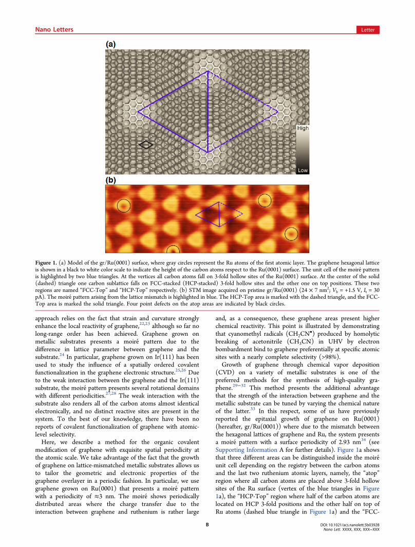
Ru(0001) surface, the moire pattern not only presents specific
atomic sites with high chemical reactivity but long-range orderas well. In this system, it is possible to grow graphene layerspresenting lateral domain sizes exceeding 300 nm.39,55 Thelarge domain size together with the exquisite spatial selectivityof our functionalization method ensures the long-range order ofthe functionalized surface. Figure 5 shows a 66 × 40 nm2 STMimage of the functionalized gr/Ru(0001). In the image 50% ofthe moire unit cells are occupied by one chemically bonded−CH2CN molecule. Of those, 98.6% are bonded in the HCP-Top areas, while only 1.4% of the −CH2CN are bonded to theFCC-TOP areas.Similar results have been obtained for propionitrile,
isobutyronitrile, and 2-phenylacetonitrile, demonstrating theapplicability of this functionalization method to other molecularspecies (see Supporting Information H for details).
Figure 4. (a) Adsorption energies calculated for the differentconfigurations of CH2CN
• on the HCP-Top (solid boxes) and onthe FCC-Top (empty boxes) regions of the gr/Ru(0001) moire. Theinset shows the ground state geometry of the corresponding moleculein the gas-phase. (b and c) Ground state adsorption geometries of thetwo most stable configurations of CH2CN
• adsorbed in the HCP-Topregion of the gr/Ru(0001) moire. Graphene atoms are colored fromdark-gray to white depending on their height. Carbon, nitrogen, andhydrogen atoms of the molecule are colored in cyan, blue, and white.
Nano Letters Letter
DOI: 10.1021/acs.nanolett.5b03928Nano Lett. XXXX, XXX, XXX−XXX
E
In conclusion, we take advantage of the nanostructurationinduced on graphene grown on Ru(0001) to chemicallyfunctionalize the graphene overlayer with atomic-levelselectivity and exquisite spatial periodicity. The comparisonbetween graphene grown on Ir(111) and graphene onRu(0001) shows the importance of the interaction betweenthe graphene and the metallic substrate that spatially modulatesthe properties of the graphene. Acetonitrile is homolyticallybroken by electron bombardment producing cyanomethylradicals that react with the nanostructured graphene in aspatially modulated fashion. These results offer the possibilityfor tuning the graphene electronic, optic, or magneticproperties through an adequate covalent functionalization ofsingle layer graphene with long-range order on the order ofhundreds of nanometers and a periodicity of almost 3 nm.Moreover, identical results were obtained for propionitrile,isobutyronitrile, and 2-phenylacetonitrile, establishing a bench-mark for the attachment of more complex molecular structuresto specific atomic sites on graphene.Methods. All experiments were performed in an UHV
chamber with a base pressure of 5 × 10⁻¹¹ Torr equipped witha low-temperature STM and facilities for tip and samplepreparation. All of the STM measurements were carried out at80 K. The graphene layer was prepared by keeping the Rucrystal at 1150 K in UHV while exposing it to an ethylenepartial pressure of 8 × 10⁻⁸ Torr for 10 min. Acetonitrile wasintroduced in the UHV chamber via a leak valve to produce apartial pressure of 1 × 10⁻⁶ Torr. The values for the partialpressures of the different gases are measured using a Bayard-Alpert gauge calibrated for N2. The details of the calculationsare provided in the Supporting Information.
■ ASSOCIATED CONTENT
*S Supporting InformationThe Supporting Information is available free of charge on theACS Publications website at DOI: 10.1021/acs.nano-lett.5b03928.
Detailed discussion of the graphene/Ru(0001) structure.Oxygen contamination identification. Wet chemistryapproach. Relative abundance of the cyanomethyl radicalversus the acetonitrile molecule. Adsorption on gra-phene/Ir(111). Theoretical calculations. Ion gauge
influence on the functionalization. Functionalizationwith different molecules (CH3CH2CN, (CH3)2CHCN,and Ph−CH2CN) (PDF)
■ AUTHOR INFORMATIONCorresponding Authors*E-mail: (A.L.V.d.P.) [email protected].*E-mail: (E.M.P.) [email protected] AddressesD.S.: Center for nanostructured Graphene, Department ofMicro- and Nanotechnology, Technical University of Denmark,Ørsteds plads, Building 345B, DK-2800 Kgs., Lyngby, Den-mark.M.G.: Physik-Department E20, TU Munchen, James-Franckstr. 1, D-85748 Garching, Germany.Author ContributionsThe experiments and data analysis were carried out primarily byF.C. and J.J.N, with important contributions by A.B. R.B.-G.and M.G. S.L. performed the wet chemistry experiments. D.S.performed the theoretical calculations and contributed to thewriting of the manuscript. D.G. contributed with the dataanalysis and contributed to the writing to the manuscript. R.M.contributed to the writing of the manuscript. E.M.P. andA.L.V.P. designed the experiments and wrote the manuscriptwith contributions from all authors.NotesThe authors declare the following competing financialinterest(s): The results here are partially protected underSpanish patent application P201530126.
■ ACKNOWLEDGMENTSFinancial support by the European Research Council (MINT,ERC-StG-2012-307609) the Ministerio de Economia yCompetit ividad (MINECO) FIS2013-40667-P andCTQ2014-60541-P, and Comunidad de Madrid through theprogramme MAD2D P2013/MIT-3007 and NanofrontmagS2013/MIT-2850 is gratefully acknowledged. D.G. acknowl-edges RyC-2012-09864. R.B.-G. acknowledges BES-2011-050821.
■ REFERENCES(1) Geim, A. K.; Novoselov, K. S. Nat. Mater. 2007, 6, 183−191.
Figure 5. STM image (66 × 40 nm2, Vb = 1.7 V, It = 30 pA) acquired at 80 K on a high coverage sample, prepared by exposing the gr/Ru(0001)surface to 600 Langmuir of acetonitrile at 300 K. The moire unit cell is highlighted in blue.
Nano Letters Letter
DOI: 10.1021/acs.nanolett.5b03928Nano Lett. XXXX, XXX, XXX−XXX
F
(2) Georgakilas, V.; Otyepka, M.; Bourlinos, A. B.; Chandra, V.; Kim,N.; Kemp, K. C.; Hobza, P.; Zboril, R.; Kim, K. S. Chem. Rev. 2012,112, 6156−6214.(3) Chua, C. K.; Pumera, M. Chem. Soc. Rev. 2013, 42, 3222−3233.(4) Park, J.; Yan, M. Acc. Chem. Res. 2013, 46, 181−189.(5) Kuila, T.; Bose, S.; Mishra, A.; Khanra, P.; Kim, N. H.; Lee, J. H.Prog. Mater. Sci. 2012, 57, 1061−1105.(6) Sun, Z.; James, D. K.; Tour, J. M. J. Phys. Chem. Lett. 2011, 2,2425−2432.(7) Criado, A.; Melchionna, M.; Marchesan, S.; Prato, M. Angew.Chem., Int. Ed. 2015, 54, 10734−10750.(8) Criado, A.; Melchionna, M.; Marchesan, S.; Prato, M. Angew.Chem., Int. Ed. 2015, 54, 2−19.(9) Schedin, F.; Geim, A. K.; Morozov, S. V.; Hill, E. W.; Blake, P.;Katsnelson, M. I.; Novoselov, K. S. Nat. Mater. 2007, 6, 652−655.(10) Garnica, M.; Stradi, D.; Barja, S.; Calleja, F.; Díaz, C.; Alcamí,M.; Vazquez de Parga, A. L.; Martín, F.; Miranda, R. Nat. Phys. 2013,9, 368−374.(11) Vinogradov, N. A.; Schulte, K.; Ng, M. L.; Mikkelsen, A.;Lundgren, E.; Martensson, N.; Preobrajenski, A. B. J. Phys. Chem. C2011, 115, 9568−9577.(12) Hossain, M. Z.; Johns, J. E.; Bevan, K. H.; Karmel, H. J.; Liang,Y. T.; Yoshimoto, S.; Mukai, K.; Koitaya, T.; Yoshinobu, J.; Kawai, M.;Lear, A. M.; Kesmodel, L. L.; Tait, S. L.; Hersam, M. C. Nat. Chem.2012, 4, 305−309.(13) Sofo, J. O.; Chaudhari, A. S.; Barber, G. D. Phys. Rev. B: Condens.Matter Mater. Phys. 2007, 75, 153401.(14) Boukhvalov, D. W.; Katsnelson, M. I.; Lichtenstein, A. I. Phys.Rev. B: Condens. Matter Mater. Phys. 2008, 77, 035427.(15) Elias, D. C.; Nair, R. R.; Mohiuddin, T. M. G.; Morozov, S. V.;Blake, P.; Halsall, M. P.; Ferrari, A. C.; Boukhvalov, D. W.; Katsnelson,M. I.; Geim, A. K.; Novoselov, K. S. Science 2009, 323, 610−613.(16) Haberer, D.; Vyalikh, D. V.; Taioli, S.; Dora, B.; Farjam, M.;Fink, J.; Marchenko, D.; Pichler, T.; Ziegler, K.; Simonucci, S.;Dresselhaus, M. S.; Knupfer, M.; Buchner, B.; Gruneis, A. Nano Lett.2010, 10, 3360−3366.(17) Park, C. H.; Yang, L.; Son, Y. W.; Cohen, M. L.; Louie, S. G.Nat. Phys. 2008, 4, 213−217.(18) Ouyang, F.; Peng, S.; Liu, Z.; Liu, Z. ACS Nano 2011, 5, 4023−4030.(19) Dvorak, M.; Oswald, W.; Wu, Z. Sci. Rep. 2013, 3, 2289.(20) Bian, S.; Scott, A. M.; Cao, Y.; Liang, Y.; Osuna, S.; Houk, K. N.;Braunschweig, A. B. J. Am. Chem. Soc. 2013, 135, 9240−9243.(21) Hossain, M. Z.; Walsh, M. A.; Hersam, M. C. J. Am. Chem. Soc.2010, 132, 15399−15403.(22) Wu, Q.; Wu, Y.; Hao, Y.; Geng, J.; Charlton, M.; Chen, S.; Ren,Y.; Ji, H.; Li, H.; Boukhvalov, D. W.; Piner, R. D.; Bielawski, C. W.;Ruoff, R. S. Chem. Commun. 2013, 49, 677−679.(23) Bissett, M. A.; Konabe, S.; Okada, S.; Tsuji, M.; Ago, H. ACSNano 2013, 7, 10335−10343.(24) Vazquez de Parga, A. L.; Miranda, R. In Graphene:Properties,preparation, characterisation and devices; Chapter 6; Skakalova, V.,Kaiser, A. B., Eds.; Woodhead Publishhing, 2014.(25) Balog, R.; Jørgensen, B.; Nilsson, L.; Andersen, M.; Rienks, E.;Bianchi, M.; Fanetti, M.; Laegsgaard, E.; Baraldi, A.; Lizzit, S.;Sljivancanin, Z.; Besenbacher, F.; Hammer, B.; Pedersen, T. G.;Hofmann, P.; Hornekaer, L. Nat. Mater. 2010, 9, 315−319.(26) Balog, R.; Andersen, M.; Jørgensen, B.; Slijvancanin, Z.;Hammer, B.; Baraldi, A.; Larciprete, R.; Hofmann, P.; Hornekaer, L.;Lizzit, S. ACS Nano 2013, 7, 3823−3832.(27) Coraux, J.; N'Diaye, A. T.; Busse, C.; Michely, T. Nano Lett.2008, 8, 565−570.(28) Loginova, E.; Nie, S.; Thurmer, K.; Bartelt, N. C.; McCarty, K.F. Phys. Rev. B: Condens. Matter Mater. Phys. 2009, 80, 085430.(29) Chae, S. J.; Gunes, F.; Kim, K. K.; Kim, E. S.; Han, G. H.; Kim,S. M.; Shin, H. J.; Yoon, S. M.; Choi, J. Y.; Park, M. H.; Yang, C. W.;Pribat, D.; Lee, Y. H. Adv. Mater. 2009, 21, 2328−2333.(30) Reina, A.; Jia, X.; Ho, J.; Nezich, D.; Son, H.; Bulovic, V.;Dresselhaus, M. S.; Kong, J. Nano Lett. 2009, 9, 30−35.
(31) Li, X.; Cai, X.; An, J.; Kim, S.; Nah, J.; Yang, D.; Piner, R.;Velamakanni, A.; Jung, I.; Tutuc, E.; Banerjee, S. K.; Colombo, L.;Ruoff, R. S. Science 2009, 324, 1312−1314.(32) Lee, Y.; Bae, S.; Jang, H.; Jang, S.; Zhu, S. E.; Sim, S. H.; Song,Y. I.; Hong, B. H.; Ahn, J. H. Nano Lett. 2010, 10, 490−493.(33) Preobrajenski, A. B.; Ng, M. L.; Vinogradov, A. S.; Martensson,N. Phys. Rev. B: Condens. Matter Mater. Phys. 2008, 78, 073401.(34) Vazquez de Parga, A. L.; Calleja, F.; Borca, B.; Hinarejos, J. J.;Passeggi, M. G. C.; Guinea, F.; Miranda, R. Phys. Rev. Lett. 2008, 100,056807.(35) Stradi, D.; Barja, S.; Díaz, C.; Garnica, M.; Borca, B.; Hinarejos,J. J.; Sanchez-Portal, D.; Alcamí, M.; Arnau, A.; Vazquez de Parga, A.L.; Miranda, R.; Martín, F. Phys. Rev. B: Condens. Matter Mater. Phys.2013, 88, 245401.(36) Stradi, D.; Barja, S.; Díaz, C.; Garnica, M.; Borca, B.; Hinarejos,J. J.; Sanchez-Portal, D.; Alcamí, M.; Arnau, A.; Vazquez de Parga, A.L.; Miranda, R.; Martín, F. Phys. Rev. Lett. 2011, 106, 186102.(37) Borca, B.; Barja, S.; Garnica, M.; Sanchez-Portal, D.; Silkin, V.M.; Chulkov, E. V.; Hermanns, C. F.; Hinarejos, J. J.; Vazquez deParga, A. L.; Arnau, A.; Echenique, P. M.; Miranda, R. Phys. Rev. Lett.2010, 105, 036804.(38) Katano, S.; Kim, Y.; Trenary, M.; Kawai, M. Chem. Commun.2013, 49, 4679−4681.(39) Borca, B.; Barja, S.; Garnica, M.; Minniti, M.; Politano, A.;Rodríguez-García, J. M.; Hinarejos, J. J.; Farías, D.; Vazquez de Parga,A. L.; Miranda, R. New J. Phys. 2010, 12, 093018.(40) Garnica, M.; Stradi, D.; Calleja, F.; Barja, S.; Díaz, C.; Alcamí,M.; Arnau, A.; Vazquez de Parga, A. L.; Martín, F.; Miranda, R. NanoLett. 2014, 14, 4560−4567.(41) Stradi, D.; Garnica, M.; Díaz, C.; Calleja, F.; Barja, S.; Alcamí,M.; Martín, N.; Arnau, A.; Vazquez de Parga, A. L.; Miranda, R.;Martín, F. Nanoscale 2014, 6, 15271−15279.(42) Barja, S.; Garnica, M.; Hinarejos, J. J.; Vazquez de Parga, A. L.;Martín, N.; Miranda, R. Chem. Commun. 2009, 46, 8198−8200.(43) Stroscio, J. A.; Eigler, D. M. Science 1991, 254, 1319−1326.(44) Hla, S.-W. J. Vac. Sci. Technol., B: Microelectron. Process. Phenom.2005, 23, 1351−1360.(45) Caillier, C.; Ki, D. K.; Lisunova, Y.; Gaponenko, I.; Paruch, P.;Morpurgo, A. F. Nanotechnology 2013, 24, 405201.(46) Lalevee, J.; Allonas, X.; Fouassier, J.-P. J. Org. Chem. 2005, 70,814−819.(47) Henry, D. J.; Parkinson, C. J.; Mayer, P. M.; Radom, L. J. Phys.Chem. A 2001, 105, 6750−6756.(48) Coote, M. L. J. Phys. Chem. A 2004, 108, 3865−3872.(49) Kukk, E.; Sankari, R.; Huttula, M.; Sankari, A.; Aksela, H.;Aksela, S. J. Electron Spectrosc. Relat. Phenom. 2007, 155, 141−147.(50) Wu, J. Q.; Beranek, I.; Fischer, H. Helv. Chim. Acta 1995, 78,194−214.(51) Wong, M. W.; Radom, L. J. Phys. Chem. 1995, 99, 8582−8588.(52) Yoshida, H.; Fujimura, Y.; Yuzawa, H.; Kumagai, J.; Yoshida, T.Chem. Commun. 2013, 49, 3793−3795.(53) Cottrell, T. L. The Strengths of Chemical Bonds; ButterworthScientific, 1978.(54) N’Diaye, A. T.; Coraux, J.; Plasa, T. N.; Busse, C.; Michely, T.New J. Phys. 2008, 10, 043033.(55) Sutter, P. W.; Flege, J. I.; Sutter, E. A. Nat. Mater. 2008, 7, 406−500.
Nano Letters Letter
DOI: 10.1021/acs.nanolett.5b03928Nano Lett. XXXX, XXX, XXX−XXX
G


![Química .y .Nanociencia .Molecular · Eugenio .Coronado .Miralles]–]-+]] +].](https://img.dokumen.tips/doc/110x75/5e3bca2bbce9e277aa221f3b/qumica-y-nanociencia-molecular-eugenio-coronado-mirallesa-.jpg)