Embed Size (px)
Citation preview

An ambient-light sensorsystem with startupcorrection for LTPS-TFT LCD
Ilku Nam1 and Doohyung Woo2a)1 Dept of EE and also with PNULG Smart Control Center, Pusan National
University, Busan 609–735, Korea2 Dept of ICEE, The Catholic University of Korea,
43–1 Yeokgok 2dong, Wonmigu, Bucheonsi, Gyeonggido 420–743, Korea
a) cowpoxcatholicackr
Abstract: An ambient-light sensor system using low-temperature
poly-silicon thin film transistors was studied, to reduce the power
consumption of mobile applications. The proposed system with
startup correction can correct the panel-to-panel variation of the
ambient-light sensors, without additional equipment. The digital
output of the readout circuit has 8 levels per decade for the input
luminance ranges from 100 to 10000 lux, and the readout rate is
40Hz. The proposed method provides maximum differential non-uniformity below 0.3 LSB.
Keywords: ambient-light sensor system, readout circuit, non-uniformity correction, LTPS TFT, LCD
Classification: Electron devices, circuits, and systems
References
[1] J. F. Wu, C. L. Wei, Y. T. Hsieh, C. L. Fang, H. H. Tsai and Y. Z. Juang:IEEE-PEDS Dig. Tech. Papers (2011) 944.
[2] K. Maeda, T. Nagai, T. Sakai, N. Kuwabara, S. Nishi, M. Satoh, T.
Matsuo, S. Kamiya, H. Katoh, M. Ohue, Y. Kubota, H. Komiya, T.
Muramatsu, M. Katayama, P. Zebedee, S. Desumvila, C. J. Brown, H.
Walton and M. Brownlow: SID symposium Digest 36 (2005) 356.
[3] H. S. Park, T. J. Ha, Y. Hong, M. K. Han, D. H. Woo, K. S. Shin and C. W.
Kim: J. SID 16 (2008) 889.
[4] F. Matsuki, K. Hashimoto, K. Sano, D. Yeates, J. R. Ayres, M. Edwards
and A. Steer: SID symposium Digest 38 (2007) 290.
1 Introduction
Active-matrix liquid-crystal display (AMLCD) has been widely used in
mobile applications. Because an LCD panel does not illuminate for itself,
the transmissive LCD uses a backlight unit (BLU), which consumes
relatively large power in the mobile LCD. To reduce BLU power
consumption, and to improve image visibility, there have been many
efforts to control BLU brightness, based on ambient-light conditions [1, 2,3]. Some of the ambient-light sensor (ALS) systems have been implemented
IEICE Electronics Express, Vol.11, No.5, 1–7
1
© IEICE 2014DOI: 10.1587/elex.11.20140086Received January 27, 2014Accepted February 04, 2014Publicized February 17, 2014Copyedited March 10, 2014
LETTER
by external chips [1]. However, a monolithic system on a glass substrate is
more efficient in reducing the production cost and complexity of a display
module. Low-temperature poly-silicon (LTPS) thin film transistors (TFTs)
can be used for a monolithic system, which integrates a photo detector,
readout circuit and analog-to-digital converter (ADC) on the same glass
substrate [2, 3].
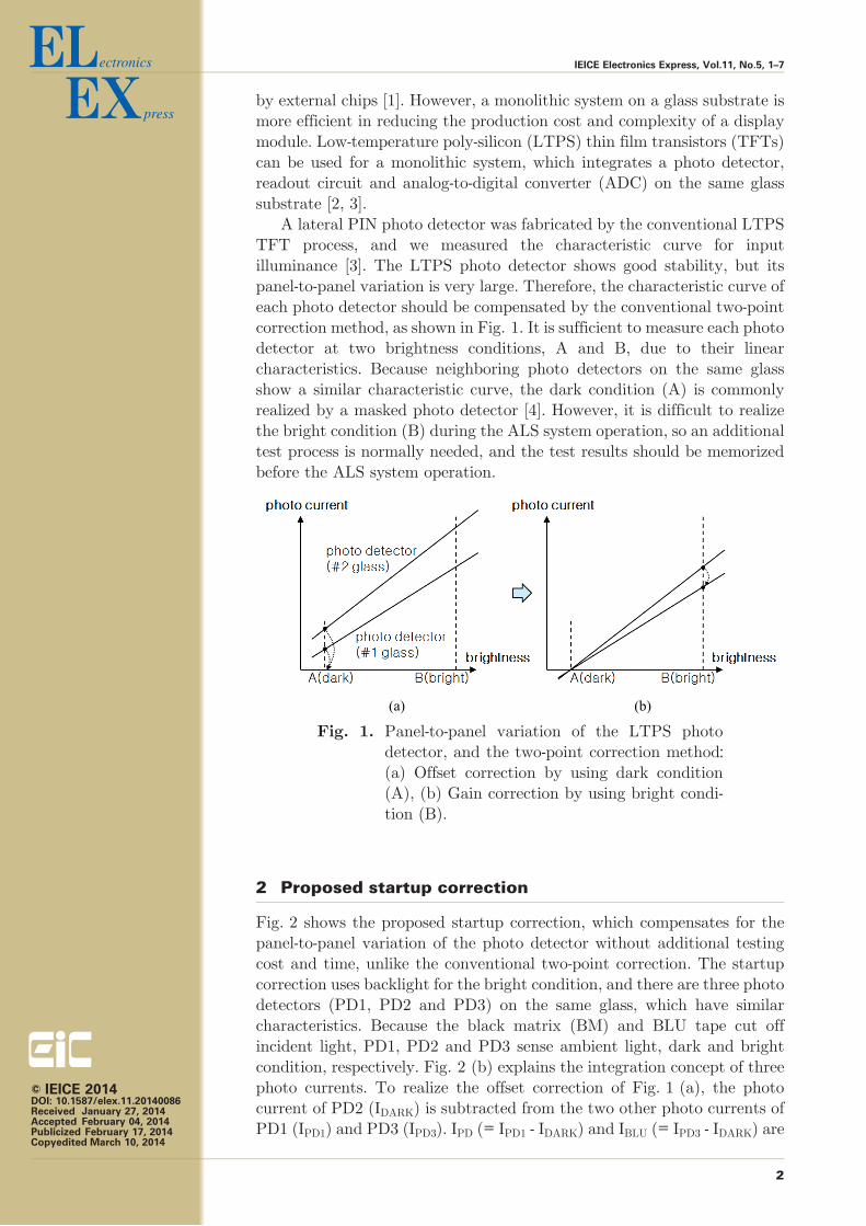
A lateral PIN photo detector was fabricated by the conventional LTPS
TFT process, and we measured the characteristic curve for input
illuminance [3]. The LTPS photo detector shows good stability, but its
panel-to-panel variation is very large. Therefore, the characteristic curve of
each photo detector should be compensated by the conventional two-pointcorrection method, as shown in Fig. 1. It is sufficient to measure each photo
detector at two brightness conditions, A and B, due to their linear
characteristics. Because neighboring photo detectors on the same glass
show a similar characteristic curve, the dark condition (A) is commonly
realized by a masked photo detector [4]. However, it is difficult to realize
the bright condition (B) during the ALS system operation, so an additional
test process is normally needed, and the test results should be memorized
before the ALS system operation.
2 Proposed startup correction
Fig. 2 shows the proposed startup correction, which compensates for the
panel-to-panel variation of the photo detector without additional testing
cost and time, unlike the conventional two-point correction. The startup
correction uses backlight for the bright condition, and there are three photo
detectors (PD1, PD2 and PD3) on the same glass, which have similar
characteristics. Because the black matrix (BM) and BLU tape cut off
incident light, PD1, PD2 and PD3 sense ambient light, dark and bright
condition, respectively. Fig. 2 (b) explains the integration concept of three
photo currents. To realize the offset correction of Fig. 1 (a), the photo
current of PD2 (IDARK) is subtracted from the two other photo currents of
PD1 (IPD1) and PD3 (IPD3). IPD (= IPD1 - IDARK) and IBLU (= IPD3 - IDARK) are
Fig. 1. Panel-to-panel variation of the LTPS photo
detector, and the two-point correction method:(a) Offset correction by using dark condition
(A), (b) Gain correction by using bright condi-tion (B).
IEICE Electronics Express, Vol.11, No.5, 1–7
2
© IEICE 2014DOI: 10.1587/elex.11.20140086Received January 27, 2014Accepted February 04, 2014Publicized February 17, 2014Copyedited March 10, 2014

the offset corrected photo current for ambient light and bright condition,
respectively. The integration period is divided into two phases. First, the
backlight has an initial brightness of LBLU, and the integrator integrates IBLUfor the pre-defined duration of tBLU. The integrated voltage after tBLU (VBLU)
is a function of the sensitivity of the photo detector (k), and is given by
VBLU ¼ k � LBLU � tBLUCINT
(1)
where CINT is the integration capacitance. Next, the integrator is reset, and
integrates IPD until the tPD, when an integrating voltage reaches the VBLU.
Now, the tPD is given as
tPD ¼ CINT � VBLU
k � LPD¼ tBLU � LBLU
LPD(2)
where LPD is the brightness of ambient light. Consequently, tPD is the gain
corrected information for ambient light, and barely related to the
sensitivity, i.e. panel-to-panel variation, because the three photo detectors
on the same glass have similar characteristics.
3 Design of a proposed circuit
Fig. 3 and Fig. 4 show the block and timing diagram of the proposed
circuit, respectively. The proposed circuit is composed of three photo
detectors with four NMOS switches, an integrator, a comparator, a 9-bitcounter, two registers and a 6-bit digital-to-analog converter (DAC). The
6-bit DAC is the resistor string converter with a tree-like decoder. There arefour control signals (1, 2, rst and S), and ck is the main clock signal.
The timing diagram is divided into three parts by 1 and 2, and rst resets
the integrator and counter periodically. During phase 1a, the voltage of the
counter enable, V(c), is kept low by 2. Therefore, the counter maintains a
Fig. 2. Proposed startup correction method with back-light unit: (a) Cross-sectional view of the three
photo detectors, (b) Timing diagram for signal
integration.
IEICE Electronics Express, Vol.11, No.5, 1–7
3
© IEICE 2014DOI: 10.1587/elex.11.20140086Received January 27, 2014Accepted February 04, 2014Publicized February 17, 2014Copyedited March 10, 2014

reset level, and it is memorized at the 6-bit register. Now, the DAC output
voltage, V(b), maintains its minimum value, Vb1. The integrator integrates
IBLU (= IPD3 - IDARK) during phase 1a, then its output voltage, V(a), reaches
VBLU after tBLU. The VBLU values of each panel are different from each
other, as shown in Fig 2 (b), and it should be converted to digital code to
keep its value, because the backlight brightness will be controlled after
phase 1a. Next, both 1 and 2 have low level in phase 1b, and V(a) remains
as VBLU ranged from Vb1 to Vb2. At the beginning of phase 1b, V(c) changes
to high level, because the comparator output voltage is high, then the
outputs of the counter, 6-bit register and V(b) increase with ck. If V(b)
begins to exceed VBLU, the comparator output voltage and V(c) change to
low level, then the counter and DAC hold their status. At the end of phase
1b, the counter output is memorized in the 6-bit register, by changing 1 to
high level, and V(b) remains as VBLU. In the last part, phase 2, the
integrator integrates IPD (= IPD1 - IDARK), after rst reset its output. The
counter output also increases with ck after resetting, because the
comparator output voltage and V(c) are low and high level at the
beginning of phase 2, respectively. If V(a) begins to exceed V(b) of VBLU, V(c)
changes to low level, then the counter holds its output, which is the digital
value of the tPD of Fig. 2 (b). Finally, the counter output is memorized in
the 9-bit register by S, and the integration and conversion cycle will go on.
The operational amplifiers in Fig. 3 are laid out using common-centroidlayout technique with large size of devices. Nevertheless, they have a large
input offset voltage (VOS) of a few hundred mV, because there are serious
mismatches among LTPS TFTs which are mainly caused by the random
distribution of grain boundaries in TFTs. However, the VOS of the
comparator does not affect correction accuracy because the stored V(b)
after phase 1b is equal to VBLU + VOS. The bias voltage of three photo
detectors is affected by the VOS of the integrator. However, PD1 and PD3
have the same bias voltage and the correction accuracy is rarely affected by
the accuracy of IDARK because IDARK is relatively small in the reverse-biased
Fig. 3. Block diagram of the readout circuit for start-upcorrection.
IEICE Electronics Express, Vol.11, No.5, 1–7
4
© IEICE 2014DOI: 10.1587/elex.11.20140086Received January 27, 2014Accepted February 04, 2014Publicized February 17, 2014Copyedited March 10, 2014

PN junction diode. Consequently, the proposed circuit is immune to the
mismatches among LTPS TFTs.
4 Simulation results
The proposed circuit has been designed using a 4-μm 1-poly 1-metal LTPS-TFT process. The mobility (μ) and threshold voltage (VTH) of n-type and
p-type TFTs are extracted from the measurement data of the fabricated
LTPS-TFT. The typical values of μn, μp, VTHn and VTHp are 120 cm2/(Vs),
80 cm2/(Vs), +1.5V and �1.5V, respectively. The analog circuit uses 6-Vand �3-V supplies, and the digital circuit uses only 6-V supply. The
maximum integration time is 23ms, and the total power consumption is
less than 150μW, when the conversion rate is 40Hz.
The HSPICE simulations were performed using the Rensselaer Poly-technic Institute (RPI) poly-silicon TFT model. Fig. 5 shows the simulated
voltage waveforms of the proposed circuit in Fig. 3. Fig. 6 compares the
simulated output of the counter using proposed startup correction with
that of the counter without startup correction. We assumed that the
maximum photo-response non-uniformity (PRNU) of the photo detectors
on the same glass is 5% or 10%, and the panel-to-panel variation is 100%.
The reference case in Fig. 6 was obtained from the photo detector with the
minimum photo responsivity. On the other hand, the other three cases were
obtained from the photo detectors whose photo responsivities have twice
values (100% variation) of the reference case’s photo responsivity. The
counter output with the startup correction has more uniform character-istics compared with that without the startup correction.
As shown in Fig. 7, the counter output is converted to the final digital
code of 16 levels, in order to divide the input ambient-light luminance on
the logarithmic axis, which ranges from 100 to 10000 lux, into eight sections
per decade. The maximum differential non-uniformity (DNU) of the final
digital code, which is similar to the differential nonlinearity (DNL), is
defined as the difference between all the possible input ranges of each
digital code and the ideal value. Although the panel-to-panel variation is
large, the DNU of the proposed monolithic circuit with the startup
correction is very low.
Fig. 4. Timing diagram of the readout circuit shown in
Fig. 3.
IEICE Electronics Express, Vol.11, No.5, 1–7
5
© IEICE 2014DOI: 10.1587/elex.11.20140086Received January 27, 2014Accepted February 04, 2014Publicized February 17, 2014Copyedited March 10, 2014

Fig. 5. Simulated voltage waveforms of the proposed
circuit.
Fig. 6. Transfer characteristic of the counter output
versus the input ambient-light luminance.
Fig. 7. Estimated maximum DNU of the final digital code.
IEICE Electronics Express, Vol.11, No.5, 1–7
6
© IEICE 2014DOI: 10.1587/elex.11.20140086Received January 27, 2014Accepted February 04, 2014Publicized February 17, 2014Copyedited March 10, 2014

5 Conclusion
A monolithic ambient-light sensor system with startup correction was
studied, to reduce the power consumption of the mobile applications. The
proposed startup correction can save additional testing cost and time, and
it has a very simple structure and timing to be implemented on a glass
substrate. Although we did not consider the panel-to-panel variation of the
backlight luminance, which is typically less than 10%, the proposed method
can instead reduce this effect because the proposed method senses the
relative brightness of an ambient light to control the backlight luminance.
Acknowledgments
This research was supported by Basic Science Research Program through
the National Research Foundation of Korea (NRF) funded by the Ministry
of Education (NRF-2013R1A1A2011732).
IEICE Electronics Express, Vol.11, No.5, 1–7
7
© IEICE 2014DOI: 10.1587/elex.11.20140086Received January 27, 2014Accepted February 04, 2014Publicized February 17, 2014Copyedited March 10, 2014


![IEICE Communications Society GLOBAL …cs/gnl/gnl_vol34.pdf[ Contents ] IEICE Communications Society – GLOBAL NEWSLETTER Vol. 34 1 * 2010,IEICE IEICE Communications Society GLOBAL](https://img.dokumen.tips/doc/110x75/5f0ddae77e708231d43c6b92/ieice-communications-society-global-csgnlgnlvol34pdf-contents-ieice-communications.jpg)
![IEICE Communications Society GLOBAL … 2011,IEICE [Contents] IEICE Communications Society – GLOBAL NEWSLETTER Vol. 35, No. 1 IEICE Communications Society GLOBAL NEWSLETTER Vol](https://img.dokumen.tips/doc/110x75/5ae27cfe7f8b9a5d648cc037/ieice-communications-society-global-2011ieice-contents-ieice-communications.jpg)


![LETTER IEICE Electronics Express, Vol.11, No.6, 1 6 A ...soc.yonsei.ac.kr/Abstract/International_journal/pdf/no_114_letter.pdf · LETTER [1]. The TAM through which the core can be](https://img.dokumen.tips/doc/110x75/600e714909c61c2eeb3d2a89/letter-ieice-electronics-express-vol11-no6-1-6-a-soc-letter-1-the-tam.jpg)


![IEICE Communications Society GLOBAL NEWSLETTER Vol ...dac.heteml.jp/ieice/csweb/gnl/gnl_vol36.pdf* 2012,IEICE [Contents] IEICE Communications Society – GLOBAL NEWSLETTER Vol. 36,](https://img.dokumen.tips/doc/110x75/5fa690e1f510db533874d83c/ieice-communications-society-global-newsletter-vol-dac-2012ieice-contents.jpg)