Embed Size (px)
Citation preview

1
LECTURE NOTES
ON
OPTICAL FIBER COMMUNICATION (15A04701)
2018 – 2019
IV B. Tech I Semester (JNTUA-R15)
Mrs. N.Pranavi, Assistant Professor
CHADALAWADA RAMANAMMA ENGINEERING COLLEGE (AUTONOMOUS)
Chadalawada Nagar, Renigunta Road, Tirupati – 517 506
Department of Electronics and Communication Engineering

2
SYLLABUS Optical Fiber Communication
UNIT-I Introduction to Optical Fibers: Evolution of fiber optic system- Element of an Optical
Fiber Transmission link- Ray Optics-Optical Fiber Modes and Configurations –Mode theory
of Circular Wave guides- Overview of Modes-Key Modal concepts- Linearly Polarized
Modes –Single Mode Fibers-Graded Index fiber structure.
UNIT-II
Signal Degradation Optical Fibers: Attenuation – Absorption losses, Scattering losses,
Bending Losses, Core and Cladding losses, Signal Distortion in Optical Wave guides -
Information Capacity determination –Group Delay- Material Dispersion, Wave guide
Dispersion, Signal distortion in SM fiber`s-Polarization Mode dispersion, Intermodal
dispersion, Pulse Broadening in GI fibers-Mode Coupling –Design Optimization of SM
fibers-RI profile and cut-off wavelength.
UNIT-III
Fiber Optical Sources and Coupling : Direct and indirect Band gap materials-LED
structures –Light source materials –Quantum efficiency and LED power, Modulation of a
LED, lasers Diodes-Modes and Threshold condition –Rate equations –External Quantum
efficiency –Resonant frequencies –Temperature effects, Introduction to Quantum laser,
source-to-fiber Power Launching, Lensing schemes, Fiber –to- Fiber joints, Fiber splicing.
UNIT-IV
Fiber Optical Receivers : PIN and APD diodes –Photo detector noise, SNR, Detector
Response time, Avalanche Multiplication Noise –Comparison of Photo detectors –
Fundamental Receiver Operation – preamplifiers, Error Sources –Receiver Configuration –
Probability of Error – Quantum Limit.
UNIT-V
System Designand Applications: Design of Analog Systems: system specification, power
budget, bandwidth budget.
Design of Digital Systems: system specification, rise time budget, power budget, Receiver
sensitivity.
Text Books:
1. Gerd Keiser, “Optical Fiber Communication” McGraw –Hill International, Singapore, 3rd ed.,
2000.
2. J.Senior, “Optical Communication, Principles and Practice”, Prentice Hall of India,1994.
References:
1. Max Ming-Kang Liu, “Principles and Applications of Optical Communications”,TMH, 2010.
2. S.C.Gupta, “Text book on optical fiber communication and its applications”, PHI,2005.
3. Satish Kumar, “Fundamentals of Optical Fiber communications”, PHI,
3
I.
UNIT –I
Introduction to Optical Fibers:
1.1. Historical Development
Fiber optics deals with study of propagation of light through transparent
dielectric wageguides. The fiber optics are used for transmission of data from
point to point location. Fiber optic systems currently used most extensively
as the transmission line between terrestrial hardwired systems.
The carrier frequencies used in conventional systems had the limitations in
handlinmg the volume and rate of the data transmission. The greater the
carrier frequency larger the available bandwith and information carrying
capacity.
First generation
The first generation of lightwave systems uses GaAs semiconductor laser and
operating region was near 0.8 µm. Other specifications of this generation are
as under:
i) Bit rate : 45 Mb/s
ii) Repeater spacing : 10 km
Second generation
i) Bit rate : 100 Mb/s to 1.7 Gb/s
ii) Repeater spacing : 50 km
iii) Operation wavelength : 1.3 µm
iv) Semiconductor : In GaAsP
Third generation
i) Bit rate : 10 Gb/s
ii) Repeater spacing : 100 km
iii) Operating wavelength : 1.55 µm
Fourth generation
Fourth generation uses WDM technique.
Bit rate : 10 Tb/s
Repeater spacing : > 10,000 km
Operating wavelength : 1.45 to 1.62 µm
Fifth generation

4
Fifth generation uses Roman amplification technique and optical solitiors.
Bit rate : 40 - 160 Gb/s
Repeater spacing : 24000 km - 35000 km
Operating wavelength : 1.53 to 1.57 µm
Need of fiber optic communication
Fiber optic communication system has emerged as most important
communication system. Compared to traditional system because of following
requirements :
1. In long haul transmission system there is need of low loss transmission medium
2. There is need of compact and least weight transmitters and receivers.
3. There is need of increase dspan of transmission.
4. There is need of increased bit rate-distrance product.
A fiber optic communication system fulfills these requirements, hence most
widely acception.
1.2 General Optical Fiber Communication System
Basic block diagram of optical fiber communication system consists of
following important blocks.
1. Transmitter
2. Information channel
3. Receiver.
Fig. 1.2.1 shows block diagram of OFC system.
Message origin :
Generally message origin is from a transducer that converts a non-electrical
message into an electrical signal. Common examples include microphones

5
for converting sound waves into currents and video (TV) cameras for
converting images into current. For data transfer between computers, the
message is already in electrical form.
Modulator :
The modulator has two main functions.
1) It converts the electrical message into the proper format.
2) It impresses this signal onto the wave generated by the carrier source.
Two distinct categories of modulation are used i.e. analog modulation
and digital modulation.
Carrier source :
Carrier source generates the wave on which the information is transmitted.
This wave is called the carrier. For fiber optic system, a laser diode (LD) or a
light emitting diode (LED) is used. They can be called as optic oscillators,
they provide stable, single frequency waves with sufficient power for long
distance propagation.
Channel coupler :
Coupler feeds the power into the information channel. For an atmospheric
optic system, the channel coupler is a lens used for collimating the light
emitted by the source and directing this light towards the receiver. The
coupler must efficiently transfer the modulated light beam from the source to
the optic fiber. The channel coupler design is an important part of fiber
system because of possibility of high losses.
Information channel :
The information channel is the path between the transmitter and receiver. In
fiber optic communications, a glass or plastic fiber is the channel. Desirable
characteristics of the information channel include low attenuation and large
light acceptance cone angle. Optical amplifiers boost the power levels of
weak signals. Amplifiers are needed in very long links to provide sufficient
power to the receiver. Repeaters can be used only for digital systems. They
convert weak and distorted optical signals to electrical ones and then
regenerate the original disgital pulse trains for further transmission.
Another important property of the information channel is the propagation
time of the waes travelling along it. A signal propagating along a fiber
normally contains a range of optic frequencies and divides its power along
several ray paths. This results in a distortion of the propagating signal. In a
digital system, this distortion appears as a spreading and deforming of the
pulses. The spreading is so great that adjacent pulses begin to overlap and
become unrecognizable as separate bits of information.

6
Optical detector :
The information being transmitted is detector. In the fiber system the optic
wave is converted into an electric current by a photodetector. The current
developed by the
detector is proportional to the power in the incident optic wave. Detector
output current contains the transmitted information. This detector output is
then filtered to remove the constant bias and thn amplified.
The important properties of photodetectors are small size, economy, long life,
low power consumption, high sensitivity to optic signals and fast response to
quick variations in the optic power.
Signal processing :
Signal processing includes filtering, amplification. Proper filtering
maximizes the ratio of signal to unwanted power. For a digital system
decision circuit is an additional block. The bit error rate (BER) should be
very small for quality communications.
Message output :
The electrical form of the message emerging from the signal processor are
transformed into a soud wave or visual image. Sometimes these signals are
directly usable when computers or other machines are connected through a
fiber system.
1.3 Advantages of Optical Fiber Communications
1. Wide bandwidth
The light wave occupies the frequency range between 2 x 10¹² Hz to 3.7 x
1012 Hz. Thus the information carrying capability of fiber optic cables is
much higher.
2. Low losses
Fiber optic cables offers bery less signal attenuation over long distances.
Typically it is less than 1 dB/km. This enables longer distance between
repeaters.
3. Immune to cross talk
Fiber optic cables has very high immunity to electricaland magnetic field.
Since fiber optic cables are non-conductors of electricity hence they do not
produce magnetic field. Thus fiber optic cables are immune to cross talk
between cables cause dby magnetic induction.
4. Interference immune

7
Fiber optic cable sar eimmune to conductive and radiative interferences
caused by electrical noise sources such as lighting, electric motors,
fluorescent lights.
5. Light weight
As fiber cables are made of silica glass or plastic which is much lighter than
copper or aluminium cables. Light weight fiber cables are cheaper to
transport.
6. Small size
The diameter of fiber is much smaller compared to other cables, therefore
fiber calbe is small in size, requires less storage space.
7. More strength
Fiber cables are stronger and rugged hence can support more weight.
8. Security
Fiber cables are more secure than other cables. It is almost impossible to tap
into a fiber cable as they do n ot radiate signals.
No ground loops exist between optical fibers hence they are more secure.
9. Long distance transmission
Becaujse of less attenuation transmission at a longer distance is possible.
10. Environment immune
Fiber calbes are more immune to environmental extremes. They can operate
over a large temperature varioations. Also they are not affected by corrosive
liquids and gases.
11. Sage and easy installation
Fiber cables are safer and easier to install and maintain. They are non-
conductors hence there is no shock hazards as no current or voltage is
associated with them. Their small size and light weight feature makes
installation easier.
12. Less cost
Cost of fiber optic system is less compated to any other system.
1.4 Disadvantages of Optical Fiber Communicaitons
1. High initial cost
The intial cost of installation or setting up cost is very high compared to all other
system.

8
2. Maintenance and repaiding cost
The maintenance and repaiding of fiber optic systems is not only difficult but
expensive also.
3. Jointing and test procedures
Since optical fibers are of very small size. The fiber joining process is very
constly and requires skilled manpower.
4. Tensile stress
Optical fibers are more susceptible to buckling, bending and tensile stress
than copper cables. This leades to restricted practice to use optical fiber
technology to premises and floor backbones with a few interfaces to the
copper cables.
5. Short links
Eventhough optical fiber calbes are inexpensive, it is still not cost effective to
replace every small conventional connector (e.g. between computers and
peripherals), as the price of optoelectronic transducers are very high.
6. Fiber losses
The amount of optical fiber available to the photodetector at the end of fiber
length depends on various fiber losses such as scattering, dispersion,
attenuation and reflection.
1.5 Applications of Optical Fiber Communicaitons
Applications of optical fiber communications include telecommunications,
data communications, video control and protection switching, sensors and
power applications.
1. Telephone networks
Optical waveguide has low attenuation, high transmission bandwidth
compated to copper lines, therefore numbers of long haul co-axial trunks
l;links between telephone exchanges are being replaced by optical fiber links.
2. Urban broadband service networks
Optical waveguide provides much larger bandwidth than co-axial calbe, also
the number of repeaters required is reduced considerably.
Modern suburban communications involves videotext, videoconferencing
videotelephony, switched broadband communication network. All these can
9
be supplied over a single fiber optic link. Fiber optic calbes is the solution to
many of today’s high speed, high bandwidth data communication problems
and will continue to play a large role in future telecom and data-com
networks.
1.6 Optical Fiber Waveguides
In free space light ravels as its maximum possible speed i.e. 3 x 10⁸ m/s or
186 x 103 miles/sec. When light travels through a material it exnibits certain
behavior explaned by laws of reflection, refraction.
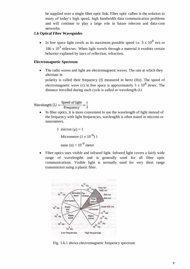
Electromagnetic Spectrum
The radio waves and light are electromagnetic waves. The rate at which they
alternate inpolarity is called their frequency (f) measured in hertz (Hz). The speed of
electromagnetic wave (c) in free space is approximately 3 x 10⁸ m/sec. The
distance travelled during each cycle is called as wavelength (λ)
In fiber optics, it is more convenient to use the wavelength of light instead of
the frequency with light frequencies, wavlengfth is often stated in microns or
nanometers.
1 micron (µ) = 1
Micrometre (1 x 10⁻⁶
) 1
nano (n) = 10-9
metre
Fiber optics uses visible and infrared light. Infrared light covers a fairly wide
range of wavelengths and is generally used for all fiber optic
communications. Visible light is normally used for very short range
transmission using a plastic fiber.
Fig. 1.6.1 shows electromagnetic frequency spectrum

10
Ray Transmission Theory
Before studying how the light actually propagates through the fiber, laws
governing the nature of light m ust be studied. These was called as laws of
optics (Ray theory). There is conception that light always travels at the same
speed. This fact is simply not true. The speed of light depends upon the
material or medium through which it is moving. In free space light travels at
its maximum possible speed i.e. 3 x 10⁸ m/s or 186 x 103 miles/sec. When
light travels through a material it exhibits certain behavior explained by laws
of reflection, refraction.
Reflection
The law of reflection states that, when a light ray is incident upon a reflective
surface at some incident angle 1 from imaginary perpendicular normal, the
ray will be reflected from the surface at some angle 2 from normal which is
equal to the angle of incidence.
Fig. 1.6.2 shows law of reflection.
Refraction
Refraction occurs when light ray passes from one medium to another i.e. the
light ray changes its direction at interface. Refraction occurs whenever
density of medium changes. E.g. refraction occurs at air and water interface,
the straw in a glass of water will appear as it is bent.
The refraction can also observed at air and glass interface.
When wave passes through less dense medium to more dense medium, the
wave is refracted (bent) towards the normal. Fig. 1.6.3 shows the refraction
phenomena.
The refraction (bending) takes place because light travels at different speed in
different mediums. The speed of light in free space is higher than in water or
glass.

11
Fig.1.6.3 Refraction
Refractive Index
The amount of refraction or bending that occurs at the interface of two
materials of different densities is usually expressed as refractive index of two
materials. Refractive index is also known as index of refraction and is
denoted by n.
Based on material density, the refractive index is expressed as the ratio of the
velocity of light in free space to the velocity of light of the dielectric material
(substance).
The refractive index for vacuum and air os 1.0 for water it is 1.3 and for glass
refractive index is 1.5.
Snell’s Law
Snell’s law states how light ray reacts when it meets the interface of two
media having different indexes of refraction.
Let the two medias have refractive indexes n1 and n2 where n1 >n2.
1 and 2 be the angles of incidence and angle of refraction respectively.
Then according to Snell’s law, a relationship exists between the refractive index of
both materials given by
n1 sin1 = n2 sin2 … (1.6.1)
A refractive index model for Snell’s law is shown in Fig. 1.6.4.
The refracted wave will be towards the normal when n1 < n2 and will away
from it when n1 > n2.

12
Equation (1.6.1) can be written as,
Fig 1.6.4 Refractive model for Snells Law
This equation shows that the ratio of refractive index of two mediums is
inversely proportional to the refractive and incident angles.
As refractive index and substituting these values in equation (1.6.2)
Critical Angle
When the angle of incidence (1) is profressively increased, there will be
progressive increase of refractive angle (2). At some condition (1) the
refractive angle (2) becomes
90o to the normal. When this happens the refracted light ray travels along the
interface. The angle of incidence (1) at the point at which the refractive
angle (1) becomes 90o is called the critical angle. It is denoted by c.
The critical angle is defined as the minimum angle of incidence (1) at
which the ray strikes the interface of two media and causes an agnle of
refraction (2) equal to 90o. Fig 1.6.5 shows critical angle refraction.

13
Fig.1.6.5 Critical Angle
Hence at critical angle 1 = c and 2 = 90o
Using Snell’s law : n1 sin 1 = n2 sin 2
Therefore,
…
(1.6
.3)
The actual value of critical angle is dependent upon combination of materials
present on each side of boundary.
Total Internal Refleciton (TIR)
When the incident angle is increase dbeyond the critical angle, the light ray
does not pass through the interface into the other medium. This gives the
effect of mirror exist at theinterface with no possibility of light escaping outside the medium. In this
condition angle of reflection (2) is equal to angle of incidence (1). This
action is called as Total Internal Reflection (TIR) of the beam. It is TIR
that leads to the propagation of waves within fiber-cable medium. TIR can be
observed only in materials in which the velocity of light is less than in air.
The refractive index of first medium must be greater than the refractive index of
second one.
1. The angle of incidence must be greater than (or equal to) the critical angle.
Example 1.6.1 : A light ray is incident from medium-1 to medium-2. If the
refractive indices of medium-1 and medium-2 are 1.5 and 1.36 respectively then
determine the angle of refraction for an angle of incidence of 30o.

14
Solution : Medium-1 n1 = 1.5
Medium-2 n2 = 1.36
Angle of incidence 1 = 30o.
Angle of incident 2 = ?
Angle of refraction 33.46o from normal. … Ans.
Example 1.6.2 : A light ray is incident from glass to air. Calculate the critical angle (c).
Solution : Refractive index of glass n1 = 1.50
Refrative indes of air n2 = 1.00
Example 1.6.3 : Calculate the NA, acceptance angle and critical angle of the fiber
having n1 (Core refractive index) = 1.50 and refractive index of cladding = 1.45.
Soluiton : n1 = 1.50, n2 = 1.45
Optical Fiver as Waveguide

15
An optical fiber is a cylindrical dielectric waveguide capable of conveying
electromagnetic waves at optical frequencies. The electromagnetic energy is
in the form of the light and propagates along the axis of the fiber. The
structural of the fiver determines the transmission characteristics.
The propagation of light along the waveguide is decided by the modes of the
waveguides, here mode means path. Each mode has distict pattern of electric
and magnetic field distributions along the fiber length. Only few modes can
satisfy the homogeneous wave
equation in the fiver also the boundary condition a waveguide surfaces.
When there is only one path for light to follow then it is called as single
mode propagation. When there is more than one path then it is called as
multimode propagation.
Single fiber structure
A single fiber structure is shown in Fig. 1.6.6. It consists of a solid dielectric
cylinder with radius ‘a’. This cylinder is called as core of fiber. The core is
surrounded by dielectric, called cladding. The index of refraction of core
(glass fiber) is slightly greater than the index of refraction of cladding.
If refractive index of core (glass fiver) = n1
and refractive index of cladding = n2
then n1 > n2.
Fig.1.6.6. Single optical Fibre Structure
Propagation in Optical Fiber
To understand the general nature of light wave propagation in optical fiber.
We first consider the construction of optical fiber. The innermost is the glass
core of very thin diameter with a slight lower refractive index n2. The light
wave can propagate along such a optical fiber. A single mode propagation is
illustrated in Fig. 1.6.7 along with standard size of fiber.
Single mode fibers are capable of carrying only one signal of a specific wavelength.
In multimode propagation the light propagates along the fiber in zigzag
fashion, provided it can undergo total internal reflection (TIR) at the core
cladding boundaries. Total internal reflection at the fiber wall can occur only if two conditions are
satisfied.
Condition 1:

16
The index of refraction of glass fiber must be slightly greater than the index of
refraction of material surrounding the fiber (cladding).
If refractive index of glass fiber = n1
and refractive index of cladding = n2
then n1 > n2.
Condition 2 :
The angle of incidence (1of light ray must be greater than critical angle (c).
A light beam is focused at one end of cable. The light enters the fibers at different
angles.Fig. 1.6.8 shows the conditions exist at the launching end of optic fiber. The
light source is surrounded by air and the refractive index of air is n0 = 1. Let
the incident ray makes an angle 0 with fiber axis. The ray enters into glass
fiber at point P making refracted angle 1 to the fiber axis, the ray is then
propagated diagonally down the core and reflect from the core wall at point Q. When the light ray reflects off the inner surface, the angle of incidence is equal to the angle of reflection, which is greater than critical angle.
In order for a ray of light to propagate down the cable, it must strike the core
cladding interface at an angle that is greater than critical angle (c).
Acceptance Angle
Applying Snell’s law to external incidence angle.
n0 sin 0 = n1 sin 1
But 1 = (90 - c)
sin 1 = sing (90 - c) = cos c
Substituting sin 1 in above equation.
n0 sin 0 = n1 cos c
Applying Pythagorean theorem to ΔPQR.

17
The maximum value of external incidence angle for which light will propagate in the
fiber.
When the light rays enters the fivers from an air medium n0 = 1. Then
above equation reduces to,
The angle 0 is called as acceptance angle and defines the
maximum angle in which the light ray may incident on fiber to propagate down
the fiber.
Acceptance Cone
Rotating the acceptance angle around the fiber axis, a cone shaped
pattern is obtained, it is called as acceptance cone of the fiber input. Fig
1.6.10 shows formation of acceptance cone of a fiber cable.
FIG: 1.6.10 shows formation of acceptance cone of a fiber cable.
The Cone of acceptance is the angle within which the light is accepted into
the core and is able to travel along the fiber. The launching of light wave
becomes easier for large acceptance come.
The angle is measured from the axis of the positive cone so the total angle of
convergence is actually twice the stated value.
Numerical Aperture (NA)
The numerical aperture (NA) of a fiber is a figure of merit which represents
its light gathering capability. Larger the numerical aperture, the greater the

18
amount of light accepted by fiber. The acceptance angle also determines how
much light is able to be enter the fiber and hence there is relation between the
numerical aperture and the cone of acceptance.
Numerical aperture (NA) = sin
For air no = 1
…
(1.6
.4)
Hence acceptance angle = sin-1
NA
By the formula of NA note that the numerical aperture is effectively
dependent only on refractive indices of core and cladding material. NA is not a
function of fiber dimension.
The index difference (Δ) and the numerical aperture (NA) are related to the
core and cladding indices:
Also Example 1.6.5 : Calculate the numerical aperture and acceptance angle for a fiber
cable of which ncore = 1.5 and ncladding = 1.48. The launching takes place from air.
Solution :
NA = 0.244 …Ans.
Acceptance angle –
Acceptance angle = sin-1
0.244

19
0 = 14.12o …Ans.
Types of Rays
If the rays are launched within core of acceptance can be successfully
propagated along the fiber. But the exact path of the ray is determined by the
position and angle of ray at which it strikes the core.
There exists three different types of rays.
i) Skew rays ii) Meridional rays iii) Axial rays.
The skew rays does not pass through the center, as show in Fig. 1.6.11 (a).
The skew rays reflects off from the core cladding boundaries and again
bounces around the outside of the core. It takes somewhat similar shape of
spiral of helical path.
Fig:1.6.11 Different Ray Propagation
The meridional ray enters the core and passes through its axis. When the
core surface is parallel, it will always be reflected to pass through the enter.
The meridional ray is shown in fig. 1.6.11 (b).
The axial ray travels along the axis of the fiber and stays at the axis all the
time. It is shown in fig. 1.6.11 (c).
Modes of Fiber
Fiber cables cal also be classified as per their mode. Light rays propagate as
an electromagnetic wave along the fiber. The two components, the electric
field and the magnetic field form patterns across the fiber. These patterns are
called modes of transmission. The mode of a fiber refers to the number of
paths for the light rays within the cable. According to modes optic fibers can
be classified into two types.i) Single mode fiber ii) Multimode fiber.

20
Multimode fiber was the first fiber type to be manufactured and
commercialized. The term multimode simply refers to the fact that numerous
modes (light rays) are carried simultaneously through the waveguide.
Multimode fiber has a much larger diameter, compared to single mode fiber,
this allows large number of modes.
Single mode fiber allows propagation to light ray by only one path. Single
mode fibers are best at retaining the fidelity of each light pulse over longer
distance also they do not exhibit dispersion caused by multiple modes.
Thus more information can be transmitted per unit of time.
This gives single mode fiber higher bandwidth compared to multimode fiber.
Some disadvantages of single mode fiber are smaller core diameter makes
coupling light into the core more difficult. Precision required for single mode
connectors and splices are more demanding.
Fiber Profiles
A fiber is characterized by its profile and by its core and cladding diameters.
One way of classifying the fiber cables is according to the index profile at
fiber. The index profile is a graphical representation of value of refractive
index across the core diameter. There are two basic types of index profiles.
i) Step index fiber. ii) Graded index fiber.
Fig. 1.6.12 shows the index profiles of fibers.
Step Index (SI) Fiber
The step index (SI) fiber is a cylindrical waveguide core with central or inner
core has a uniform refractive index of n1 and the core is surrounded by outer
cladding with uniform refractive index of n2. The cladding refractive index
(n2) is less than the core refractive index (n1). But there is an abrupt change
in the refractive index at the core cladding interface. Refractive index profile of step indexed optical fiber is shown in Fig. 1.6.13. The refractive index is plotted on horizontal axis and radial distance from the core is plotted on vertical axis.

21
The propagation of light wave within the core of step index fiber takes
the path of meridional ray i.e. ray follows a zig-zag path of straight line
segments.The core typically has diameter of 50-80 µm and the cladding has a diameter of 125
µm. The refractive index profile is defined as –
Graded Index (GRIN) Fiber
The graded index fiber has a core made from many layers of glass.
In the graded index (GRIN) fiber the refractive index is not uniform within
the core, it is highest at the center and decreases smoothly and continuously
with distance towards the cladding. The refractive index profile across the
core takes the parabolic nature. Fig. 1.6.14 shows refractive index profile of
graded index fiber.
In graded index fiber the light waves are bent by refraction towards the core
axis and they follow the curved path down the fiber length. This results
because of change in refractive index as moved away from the center of the
core.
A graded index fiber has lower coupling efficiency and higher bandwidth
than the step index fiber. It is available in 50/125 and 62.5/125 sizes. The
50/125 fiber has been optimized for long haul applications and has a smaller
NA and higher bandwidth. 62.5/125 fiber is optimized for LAN applications
which is costing 25% more than the 50/125 fiber cable. The refractive index variation in the core is giver by relationship
where,

22
r = Radial distance from fiber axis
a = Core radius
n1= Refractive index of core
n2 = Refractive index of cladding
α = Shape of index profile.
Profile parameter α determines the characteristic refractive index profile of
fiber core. The range of refractive index as variation of α is shown in Fig.
1.6.1
Comparison of Step Index and Graded Index Fiber
Sr.
No
. Parameter Step index fiber
Graded index
fiber
1. Data rate Slow. Higher
2. Coupling efficiency
Coupling efficiency with fiber
Lower coupling efficiency.
is higher.
3. Ray path By total internal reflection.
Light travelled
In
oscillatory fashion.
4. Index variation
5. Numerical aperture NA remains same. Changes continuously
With
distance from fiber axis.
6. Material used
Normally plastic or glass is
Only glass is preferred.
preferred.
7. Bandwidth 10 – 20 MHz/km 1 GHz/km
efficiency
8. Pulse spreading
Pulse spreading by fiber
Pulse spreading is less
length is more.
9. Attenuation Less typically 0.34 More 0.6 to 1 dB/km at 1.3

23
of light dB/km at 1.3 µm. µm.
10 Typical light
source LED. LED, Lasers.
Applications Subscriber local network
Local
and
wide
Area
communicat
ion. networks.
Optic Fiber Configurations
Depending on the refractive index profile of fiber and modes of fiber there
exist three types of optical fiber configurations. These optic-fiber
configurations are -
i) Single mode step index fiber. ii) Multimode step index fiber. iii) Multimode graded index fiber.
Single mode Step index Fiber
In single mode step index fiber has a central core that is sufficiently small so
that there is essentially only one path for light ray through the cable. The
light ray is propagated in the fiber through reflection. Typical core sizes are 2
to 15 µm. Single mode fiber is also known as fundamental or monomode
fiber.
Fig. 1.6.16 shows single mode fiber.
Single mode fiber will permit only one mode to propagate and does not suffer
from mode delay differences. These are primarily developed for the 1300 nm
window but they can be also be used effectively with time division multiplex
(TDM) and wavelength division multiplex (WDM) systems operating in
1550 nm wavelength region.
The core fiber of a single mode fiber is very narrow compared to the
wavelength of light being used. Therefore, only a single path exists through
the cable core through which light can travel. Usually, 20 percent of the light
in a single mode cable actually

24
travels down the cladding and the effective diameter of the cable is a blend of
single mode core and degree to which the cladding carries light. This is
referred to as the ‘mode field diameter’, which is larger than physical
diameter of the core depending on the refractive indices of the core and
cladding.
The disadvantage of this type of cable is that because of extremely small size
interconnection of cables and interfacing with source is difficult. Another
disadvantage of single mode fibers is that as the refractive index of glass
decreases with optical wavelength, the light velocity will also be wavelength
dependent. Thus the light from an optical transmitter will have definite
spectral width.
Multimode step Index Fiber
Multimode step index fiber is more widely used type. It is easy to
manufacture. Its core diameter is 50 to 1000 µm i.e. large aperture and allows
more light to enter the cable. The light rays are propagated down the core in
zig-zag manner. There are many many paths that a light ray may follow
during the propagation.
The light ray is propagated using the principle of total internal reflection
(TIR). Since the core index of refraction is higher than the cladding index of
refraction, the light enters at less than critical angle is guided along the fiber.
Light rays passing through the fiber are continuously reflected off the glass
cladding towards the centre of the core at different angles and lengths,
limiting overall bandwidth.
The disadvantage of multimode step index fibers is that the different optical
lengths caused by various angles at which light is propagated relative to the
core, causes the
transmission bandwidth to be fairly small. Because of these limitations,
multimode step index fiber is typically only used in applications requiring
distances of less than 1 km.
Multimode Graded Index Fiber

25
The core size of multimode graded index fiber cable is varying from 50 to
100 µm range. The light ray is propagated through the refraction. The light
ray enters the fiber at
many different angles. As the light propagates across the core toward the
center it is intersecting a less dense to more dense medium. Therefore the
light rays are being constantly being refracted and ray is bending
continuously. This cable is mostly used for long distance communication.
Fig 1.6.18 shows multimode graded index fiber.
The light rays no longer follow straight lines, they follow a serpentine path
being gradually bent back towards the center by the continuously declining
refractive index. The modes travelling in a straight line are in a higher
refractive index so they travel slower than the serpentine modes. This reduces
the arrival time disparity because all modes arrive at about the same time.
Fig 1.6.19 shows the light trajectory in detail. It is seen that light rays running
close to the fiber axis with shorter path length, will have a lower velocity
because they pass through a region with a high refractive index.
Rays on core edges offers reduced refractive index, hence travel more faster
than axial rays and cause the light components to take same amount of time
to travel the length of fiber, thus minimizing dispersion losses. Each path at a
different angle is termed as‘transmission mode’ and the NA of graded index fiber is defined as the
maximum value of acceptance angle at the fiber axis.

26
Typical attenuation coefficients of graded index fibers at 850 nm are 2.5 to 3
dB/km, while at 1300 nm they are 1.0 to 1.5 dB/km. The main advantages of graded index fiber are:
1. Reduced refractive index at the centre of core. 2. Comparatively cheap to produce.
Standard fibers
Cladding Core
Sr. No.
Fiber
type
Diamete
r
diam
eter Applicatio
ns
(µm) (µm)
1.
Single mode
125 8
0.1% to
0.2%
1. Long distance
(8/125)
2. High
data rate
2.
Multimode
125 50
1% to
2%
1. Short distance
(50/125)
2. Low data
rate
3.
Multimo
de 125 62.5
1% to
2% LAN (62.5/12
5)
4.
Multimode
140 100
1% to
2% LAN (100/140
)
1.7 Mode Theory for Cylindrical Waveguide
To analyze the optical fiber propagation mechanism within a fiber, Maxwell
equations are to solve subject to the cylindrical boundary conditions at core-
cladding interface. The core-cladding boundary conditions lead to coupling
of electric and magnetic field components resulting in hybrid modes. Hence
the analysis of optical waveguide is more complex than metallic hollow
waveguide analysis.
Depending on the large E-field, the hybrid modes are HE or EH modes. The
two lowest order does are HE11 and TE01.
Overview of Modes
The order states the number of field zeros across the guide. The electric fields
are not completely confined within the core i.e. they do not go to zero at
core-cladding interface and extends into the cladding. The low order mode
confines the electric field near the axis of the fiber core and there is less
penetration into the cladding. While the high order mode distribute the field
towards the edge of the core fiber and penetrations into the cladding.
Therefore cladding modes also appear resulting in power loss.
In leaky modes the fields are confined partially in the fiber core attenuated as
they propagate along the fiber length due to radiation and tunnel effect.

27
Therefore in order to mode remain guided, the propagation factor β must
satisfy the condition
n2k < β < n1k
where, n1 = Refractive index of fiber core
n2 = Refractive index of cladding
k = Propagation constant = 2π / λ
The cladding is used to prevent scattering loss that results from core material
discontinuities. Cladding also improves the mechanical strength of fiber core
and reducessurface contamination. Plastic cladding is commonly used. Materials used for
fabrication of optical fibers are silicon dioxide (SiO2), boric oxide-silica.
Summary of Key Modal Concepts
Normalized frequency variable, V is defined as
…
(1.7
.1)
where, a = Core radius
λ = Free space wavelength
Since = NA … (1.7.2)
The total number of modes in a multimode fiber is given by
Example 1.7.1 : Calculate the number of modes of an optical fiber having diameter of 50
µm, n1 = 1.48, n2 = 1.46 and λ = 0.82 µm.
Solution : d = 50 µm
n1 = 1.48
n2 = 1.46
28
λ = 0.82
µm
NA = (1.482 – 1.46
2)1/2
NA = 0.243 Number of modes are given by,
M = 1083 …Ans.
Example 1.7.2 : A fiber has normalized frequency V = 26.6 and the operating wavelength is
1300nm. If the radius of the fiber core is 25 µm. Compute the numerical aperture.
Solution : V = 26.6
λ = 1300 nm = 1300 X
10-9
m
a = 25 µm = 25 X 10-
6 m
NA = 0.220 … Ans.
Example 1.7.3 : A multimode step index fiber with a core diameter of 80 µm and a
relative index difference of 1.5 % is operating at a wavelength of 0.85 µm. If the
core refractive index is 1.48, estimate the normalized frequency for the fiber and
number of guided modes.

29
[July/Aug.-2008, 6
Marks]
Solution : Given : MM step index fiber, 2 a = 80 µm
Core radians a = 40 µm
Relative index difference, = 1.5% = 0.015
Wavelength, λ = 0.85µm
Core refractive index, n1 = 1.48
Normalized frequency, V = ?
Number of modes, M = ?
Numerical aperture
= 1.48 (2 X 0.015)1/2
= 0.2563
Normalized frequency is given by,
V = 75.78 … Ans.
Number of modes is given by,
Ans
Example 1.7.4 : A step index multimode fiber with a numerical aperture of a 0.20
supports approximately 1000 modes at an 850 nm wavelength.
i) What is the diameter of its core? ii) How many modes does the fiber support at 1320 nm?
iii) How many modes does the fiber support at 1550 nm? [Jan./Feb.-2007, 10
Marks]
Solution : i) Number of modes is given by,

30
a = 60.49 µm … Ans.
ii)
M = (14.39)2 = 207.07
iii)
M = 300.63
Wave Propagation
Maxwell’s Equations
Maxwell’s equation for non-conducting medium:
X E = - ∂B /
X H = - ∂D /
. D = 0
. B 0
where,
E and H are electric and magnetic field vectors.
The relation between flux densities and filed vectors:
D = ε0 E + P
B = µ0 H + M
where,
ε0 is vacuum permittivity.

31
µ0 is vacuum permeability.
P is induced electric polarization.
M is induced magnetic polarization (M = 0, for non-magnetic silica glass)
P and E are related by:
P(r, t) = ε0
Where,
X is linear susceptibility.
Wave equation:
Fourier transform of E (r, t)
where,
n is refractive index.
α is absorption coefficient.
Both n and α are frequency dependent. The frequency dependence of n is
called as chromatic dispersion or material dispersion. For step index fiber,
Fiber Modes
Optical mode : An optical mode is a specific solution of the wave equation that
satisfies boundary conditions. There are three types of fiber modes.

32
a) Guided modes b) Leaky modes c) Radiation modes
For fiber optic communication system guided mode is sued for signal
transmission.Considering a step index fiber with core radius ‘a’. The cylindrical co-ordinates ρ, and can be used to represent boundary conditions.
The refractive index ‘n’ has values
The general solutions for boundary condition of optical field under guided mode
is
infinite at and decay to zero at . Using Maxwell’s equation in
the core region.
The cut-off condition is defined as –
It is also called as normalized frequency.
Graded Index Fiber Structure
The Refractive index of graded index fiber decreases continuously towards
its radius from the fiber axis and that for cladding is constant.
The refractive index variation in the core is usually designed by using power
law relationship.

33
Where, r = Radial distance from fiber axis
a = Core radius
n1 = Refractive index core
n2 Refractive index of cladding and
α = The shape of the index profile
For graded index fiber, the index difference is given by,
In graded index fiber the incident light will propagate when local numerical
aperture at distance r from axis, NA is axial numerical aperture NA(0). The
local numerical aperture is given as,
The axial numerical aperture NA(0) is given as,
Hence Na for graded index decreases to zero as it moves from fiber axis to core-
cladding boundary.
The variation of NA for different values of α is shown in Fig. 1.7.1.
The number of modes for graded index fiber in given as,
…
1.8 Single Mode Fibers
Propagation in single mode fiber is advantageous because signal dispersion
due to delay differences amongst various modes in multimode is avoided.
Multimode step index fibers cannot be used for single mode propagation due
to difficulties in maintaining single mode operation. Therefore for the
34
transmission of single mode the fiber is designed to allow propagation in one
mode only, while all other modes are attenuated by leakage or absorption. For single mode operation, only fundamental LP01 mode many exist. The
single mode propagation of LP01 mode in step index fibers is possible over the range.
The normalized frequency for the fiber can be adjusted within the range by
reducing core radius and refractive index difference < 1%. In order to obtain
single mode operation with maximum V number (2.4), the single mode fiber
must have smaller core diameter than the equivalent multimode step index
fiber. But smaller core diameter has problem of launching light into the fiber,
jointing fibers and reduced relative index difference.
Graded index fibers can also be sued for single mode operation with some
special fiber design. The cut-off value of normalized frequency Vc in single
mode operation for a graded index fiber is given by,
Example 1.8.1 : A multimode step index optical fiber with relative refractive index
difference 1.5% and core refractive index 1.48 is to be used for single mode
operation. If the operating wavelength is 0.85µm calculate the maximum core
diameter.
Solution : Given :
n1 = 1.48
∆ = 1.5 % = 0.015
λ = 0.85 µm = 0.85 x 10⁻⁶
m
Maximum V value for a fiber which gives single mode operations is 2.4.
Normalized frequency (V number) and core diameter is related by expression,
a = 1.3 µm … Ans.
Maximum core diameter for single mode operation is 2.6 µm.

35
Example 1.8.2 : A GRIN fiber with parabolic refractive index profile core has a
refractive index at the core axis of 1.5 and relative index difference at 1%. Calculate
maximum possible core diameter that allows single mode operations at λ = 1.3 µm.
Solution : Given :
for a GRIN
Maximum value of normalized frequency for single mode operation is given by,
Maximum core radius is given by expression,
a = 3.3 µm … Ans.
Maximum core diameter which allows single mode operation is 6.6 µm.
Cut-off Wavelength
One important transmission parameter for single mode fiber us cut-off
wavelength for the first higher order mode as it distinguishes the single
mode and multim0de regions.
The effective cut-off wavelength λc is defined as the largest wavelength at
which
higher order mode power relative to the fundamental mode
power is reduced to 0.1 dB. The range of cut-off wavelength
recommended to avoid modal noise and dispersion problems is : 1100 to
1280 nm (1.1 to 1.28µm) for single mode fiber at 1.3 µm. The cut-off wavelength λc can be computed from expression of normalized
frequency.
…. (1.8.1)
.... (1.8.2)

36
where,
Vc is cut-off normalized frequency.
λc is the wavelength above which a particular fiber becomes single moded.
For same fiber dividing λc by λ we get the relation as:
… (1.8.3)
But for step index fiver Vc = 2.405 then
Example 1.8.3 : Estimate cut-off wavelength for step index fiber in single mode
operation. The core refractive index is 1.46 and core radius is 4.5 µm. The relative
index difference is 0.25 %.
Solutions : Given :
n1 = 1.46
a = 4.5 µm
∆ = 0.25 % = 0.0025
Cut-off wavelength is given by,
For cut-off wavelength, Vc = 2.405
Mode Field Diameter and Spot Size
The mode filed diameter is fundamental parameter of a single mode fiber. This parameter is determined from mode field distributions of fundamental
LP01 mode. In step index and graded single mode fibers, the field amplitude distribution
is

37
approximated by Gaussian distribution. The mode Field diameter (MFD) is distance between opposite 1/e – 0.37 times the near field strength )amplitude)
and power is 1/e2 = 0.135 times.
In single mode fiber for fundamental mode, on field amplitude distribution
the mode filed diameter is shown in fig. 1.8.1.
The spot size ω0 is gives as –
MFD = 2 ω0
The parameter takes into account the wavelength dependent filed
penetration into the cladding. Fig. 1.8.2 shows mode field diameters variation
with λ.

38
QUESTIONS
1. State and explain the advantages and disadvantages of fiber optic
communication systems.
2. State and explain in brief the principle of light propagation.
3. Define following terms with respect to optical laws –
A) Reflection
B) Refraction
C) Refractive index
D) Snell’s law
E) Critical angle
F) Total internal reflection (TIR)
4. Explain the important conditions for TIR to exit in fiber.
5. Derive an expression for maximum acceptance angle of a fiber.
6. Explain the acceptance come of a fiber.
7. Define numerical aperture and state its significance also.
8. Explain the different types of rays in fiber optic.
9. Explain the
A) Step index fiber
B) Graded index fiber
10. What is mean by mode of a fiber?
11. Write short notes on following –
A) Single mode step index fiber
B) Multimode step index fiber
C) Multimode graded index fiber.

39

40
UNIT - 2
SIGNAL DEGRADATION OPTICAL FIBERS.
Introduction
One of the important property of optical fiber is signal attenuation. It is also known as
fiber loss or signal loss. The signal attenuation of fiber determines the maximum distance
between transmitter and receiver. The attenuation also determines the number of
repeaters required, maintaining repeater is a costly affair.
Another important property of optical fiber is distortion mechanism. As the signal pulse
travels along the fiber length it becomes more broader. After sufficient length the broad
pulses starts overlapping with adjacent pulses. This creates error in the receiver. Hence
the distortion limits the information carrying capacity of fiber.
2.1 Attenuation
Attenuation is a measure of decay of signal strength or loss of light power that occurs as
light pulses propagate through the length of the fiber.
In optical fibers the attenuation is mainly caused by two physical factors absorption and
scattering losses. Absorption is because of fiber material and scattering due to structural
imperfection within the fiber. Nearly 90 % of total attenuation is caused by Rayleigh
scattering only. Microbending of optical fiber also contributes to the attenuation of signal.
The rate at which light is absorbed is dependent on the wavelength of the light and the
characteristics of particular glass. Glass is a silicon compound, by adding different
additional chemicals to the basic silicon dioxide the optical properties of the glass can be
changed.
The Rayleigh scattering is wavelength dependent and reduces rapidly as the wavelength
of the incident radiation increases.
The attenuation of fiber is governed by the materials from which it is fabricated, the
manufacturing process and the refractive index profile chosen. Attenuation loss is
measured in dB/km.
Attenuation Units
As attenuation leads to a loss of power along the fiber, the output power is significantly
less than the couples power. Let the couples optical power is p(0) i.e. at origin (z = 0).
Then the power at distance z is given by,
… (2.1.1)
where, αp is fiber attenuation constant (per km).

41
This parameter is known as fiber loss or fiber attenuation.
Attenuation is also a function of wavelength. Optical fiber wavelength as a function of
wavelength is shown in Fig. 2.1.1.
Example 2.1.1 : A low loss fiber has average loss of 3 dB/km at 900 nm. Compute the length
over which –
a) Power decreases by 50 % b) Power decreases by 75 %.
Solution : α = 3 dB/km
a) Power decreases by 50 %.
is given by,
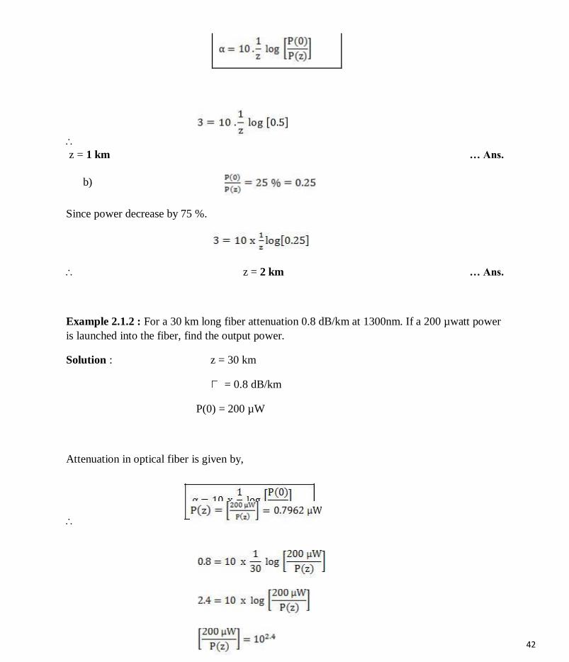
42
z = 1 km … Ans.
b)
Since power decrease by 75 %.
z = 2 km … Ans.
Example 2.1.2 : For a 30 km long fiber attenuation 0.8 dB/km at 1300nm. If a 200 µwatt power
is launched into the fiber, find the output power.
Solution : z = 30 km
= 0.8 dB/km
P(0) = 200 µW
Attenuation in optical fiber is given by,

43
Example 2.1.3 : When mean optical power launched into an 8 km length of fiber is 12 µW, the
mean optical power at the fiber output is 3 µW.
Determine –
Overall signal attenuation in dB. The overall signal attenuation for a 10 km optical link using the same fiber with splices at
1 km intervals, each giving an attenuation of 1 dB.
Solution : Given : z = 8 km
P(0) = 120 µW
P(z) = 3 µW
1) Overall attenuation is given by,
2) Overall attenuation for 10 km,
Attenuation per km
Attenuation in 10 km link = 2.00 x 10 = 20 dB
In 10 km link there will be 9 splices at 1 km interval. Each splice introducing attenuation
of 1 dB. Total attenuation = 20 dB + 9 dB = 29 dB
Example 2.1.4 : A continuous 12 km long optical fiber link has a loss of 1.5 dB/km.
What is the minimum optical power level that must be launched into the fiber to maintain
as optical power level of 0.3 µW at the receiving end? What is the required input power if the fiber has a loss of 2.5 dB/km?
[July/Aug.-2007, 6 Marks]

44
Solution : Given data : z = 12 km
= 1.5 dB/km
P(0) = 0.3 µW
Attenuation in optical fiber is given by,
= 1.80
Optical power output = 4.76 x 10⁻⁹
W … Ans.
ii) Input power = ? P(0)
When α = 2.5 dB/km

45
P(0) = 4.76 µW
Input power= 4.76 µW … Ans.
Example 2.1.5 : Optical power launched into fiber at transmitter end is 150 µW. The power at
the end of 10 km length of the link working in first windows is – 38.2 dBm. Another system of
same length working in second window is 47.5 µW. Same length system working in third
window has 50 % launched power. Calculate fiber attenuation for each case and mention
wavelength of operation. [Jan./Feb.-2009, 4 Marks]
Solution : Given data:
P(0) = 150 µW
z= 10 km
z = 10 km
Attenuation in 1st
window:
… Ans.
Attenuation in 2nd
window:
… Ans.
Attenuation in 3rd
window:
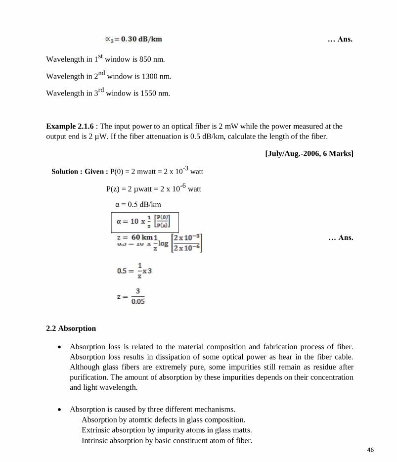
46
… Ans.
Wavelength in 1st
window is 850 nm.
Wavelength in 2nd
window is 1300 nm.
Wavelength in 3rd
window is 1550 nm.
Example 2.1.6 : The input power to an optical fiber is 2 mW while the power measured at the
output end is 2 µW. If the fiber attenuation is 0.5 dB/km, calculate the length of the fiber.
[July/Aug.-2006, 6 Marks]
Solution : Given : P(0) = 2 mwatt = 2 x 10⁻³
watt
P(z) = 2 µwatt = 2 x 10⁻⁶
watt
α = 0.5 dB/km
… Ans.
2.2 Absorption
Absorption loss is related to the material composition and fabrication process of fiber.
Absorption loss results in dissipation of some optical power as hear in the fiber cable.
Although glass fibers are extremely pure, some impurities still remain as residue after
purification. The amount of absorption by these impurities depends on their concentration
and light wavelength.
Absorption is caused by three different mechanisms.
Absorption by atomtic defects in glass composition. Extrinsic absorption by impurity atoms in glass matts. Intrinsic absorption by basic constituent atom of fiber.

47
Absorption by Atomic Defects
Atomic defects are imperfections in the atomic structure of the fiber materials such as
missing molecules, high density clusters of atom groups. These absorption losses are
negligible compared with intrinsic and extrinsic losses.
The absorption effect is most significant when fiber is exposed to ionizing radiation in
nuclear reactor, medical therapies, space missions etc. The radiation dames the internal
structure of fiber. The damages are proportional to the intensity of ionizing particles. This
results in increasing attenuation due to atomic defects and absorbing optical energy. The
total dose a material receives is expressed in rad (Si), this is the unit for measuring
radiation absorbed in bulk silicon.
1 rad (Si) = 0.01 J.kg
The higher the radiation intensity more the attenuation as shown in Fig 2.2.1.
Extrinsic Absorption
Extrinsic absorption occurs due to electronic transitions between the energy level and
because of charge transitions from one ion to another. A major source of attenuation is
from transition of metal impurity ions such as iron, chromium, cobalt and copper. These
losses can be upto 1 to 10 dB/km. The effect of metallic impurities can be reduced by
glass refining techniques.
Another major extrinsic loss is caused by absorption due to OH (Hydroxil) ions
impurities dissolved in glass. Vibrations occur at wavelengths between 2.7 and 4.2 µm.

48
The absorption peaks occurs at 1400, 950 and 750 nm. These are first, second and third
overtones respectively.
Fig. 2.2.2 shows absorption spectrum for OH group in silica. Between these absorption
peaks there are regions of low attenuation.
Intrinsic Absorption
Intrinsic absorption occurs when material is in absolutely pure state, no density variation
and inhomogenities. Thus intrinsic absorption sets the fundamental lower limit on
absorption for any particular material.
Intrinsic absorption results from electronic absorption bands in UV region and from
atomic vibration bands in the near infrared region.
The electronic absorption bands are associated with the band gaps of amorphous glass
materials. Absorption occurs when a photon interacts with an electron in the valene band
and excites it to a higher energy level. UV absorption decays exponentially with
increasing wavelength (λ).
In the IR (infrared) region above 1.2 µm the optical waveguide loss is determined by
presence of the OH ions and inherent IR absorption of the constituent materials. The
inherent IR absorption is due to interaction between the vibrating band and the
electromagnetic field of optical signal this results in transfer of energy from field to the
band, thereby giving rise to absorption, this absorption is strong because of many bonds
present in the fiber.
The ultraviolet loss at any wavelength is expressed as,
… (2.2.1)

49
where, x is mole fraction of GeO2.
λ is operating wavelength.
αuv is in dB/km.
The loss in infrared (IR) region (above 1.2 µm) is given by expression :
… (2.2.2)
The expression is derived for GeO2-SiO2 glass fiber.
2.3 Rayleigh Scattering Losses
Scattering losses exists in optical fibers because of microscopic variations in the materialdensity and composition. As glass is composed by randomly connected network of
molecules and several oxides (e.g. SiO2, GeO2 and P2O5), these are the major cause of
compositional structure fluctuation. These two effects results to variation in refractive
index and Rayleigh type scattering of light.
Rayleigh scattering of light is due to small localized changes in the refractive index of
the core and cladding material. There are two causes during the manufacturing of fiber.
The first is due to slight fluctuation in mixing of ingredients. The random changes
because of this are impossible to eliminate completely.
The other cause is slight change in density as the silica cools and solidifies. When light
ray strikes such zones it gets scattered in all directions. The amount of scatter depends on
the size of the discontinuity compared with the wavelength of the light so the shortest
wavelength (highest frequency) suffers most scattering. Fig. 2.3.1 shows graphically the
relationship between wavelength and Rayleigh scattering loss.

50
Scattering loss for single component glass is given by,
… (2.3.1)
where, n = Refractive index
kB = Boltzmann’s constant
βT = Isothermal compressibility of material
Tf = Temperature at which density fluctuations are frozen into the glass as it solidifies
(fictive temperature)
Another form of equation is
… (2.3.2)
where, P = Photoelastic coefficient
where, = Mean square refractive index fluctuation
= Volume of fiber
Multimode fibers have higher dopant concentrations and greater compositional
fluctuations. The overall losses in this fibers are more as compared to single mode fibers.Mie Scattering :
Linear scattering also occurs at inhomogenities and these arise from imperfections in the
fiber’s geometry, irregularities in the refractive index and the presence of bubbles etc.
caused during manufacture. Careful control of manufacturing process can reduce mie
scattering to insignificant levels.
2.4 Bending Loss
Losses due to curvature and losses caused by an abrupt change in radius of curvature are
referred to as ‘bending losses.’
The sharp bend of a fiber causes significant radiative losses and there is also possibility
of mechanical failure. This is shown in Fig. 2.4.1.

51
As the core bends the normal will follow it and the ray will now find itself on the wrong
side of critical angle and will escape. The sharp bends are therefore avoided. The radiation loss from a bent fiber depends on –
Field strength of certain critical distance xc from fiber axis where power is lost
through radiation. The radius of curvature R.
The higher order modes are less tightly bound to the fiber core, the higher order modes
radiate out of fiber firstly.
5 For multimode fiber, the effective number of modes that can be guided by curved fiber is where, α is graded index profile.
is core – cladding index difference.
n2 is refractive index of cladding.k is
wave propagation constant .
N∞ is total number of modes in a straight fiber.
… (2.4.2)
Microbending
Microbending is a loss due to small bending or distortions. This small microbending is
not visible. The losses due to this are temperature related, tensile related or crush related.
The effects of microbending on multimode fiber can result in increasing attenuation
(depending on wavelength) to a series of periodic peaks and troughs on the spectral
attenuation curve. These effects can be minimized during installation and testing. Fig.
2.4.2 illustrates microbening.
52
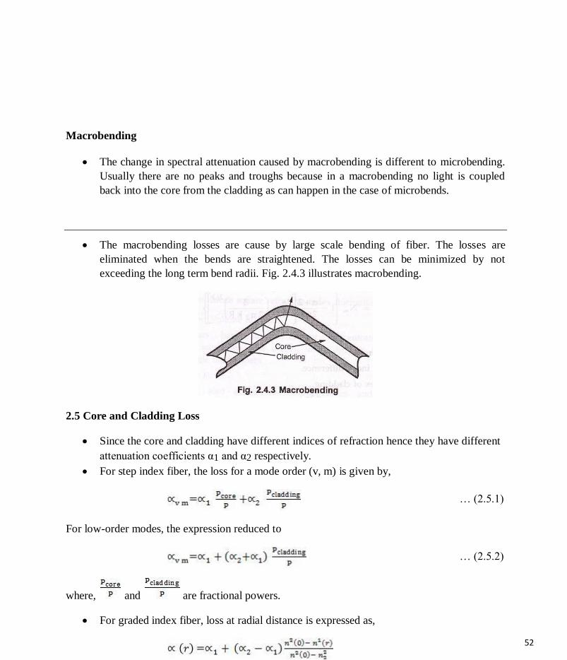
Macrobending
The change in spectral attenuation caused by macrobending is different to microbending.
Usually there are no peaks and troughs because in a macrobending no light is coupled
back into the core from the cladding as can happen in the case of microbends.
The macrobending losses are cause by large scale bending of fiber. The losses are
eliminated when the bends are straightened. The losses can be minimized by not
exceeding the long term bend radii. Fig. 2.4.3 illustrates macrobending.
2.5 Core and Cladding Loss
Since the core and cladding have different indices of refraction hence they have different
attenuation coefficients α1 and α2 respectively. For step index fiber, the loss for a mode order (v, m) is given by,
… (2.5.1)
For low-order modes, the expression reduced to
… (2.5.2)
where, and are fractional powers.
For graded index fiber, loss at radial distance is expressed as,

53
… (2.5.3)
The loss for a given mode is expressed by,
… (2.5.4)
where, P(r) is power density of that model at radial distance r.
2.6 Signal Distortion in Optical Waveguide
The pulse get distorted as it travels along the fiber lengths. Pulse spreading in fiber is
referred as dispersion. Dispersion is caused by difference in the propagation times of light
rays that takes different paths during the propagation. The light pulses travelling down
the fiber encounter dispersion effect because of this the pulse spreads out in time domain.
Dispersion limits the information bandwidth. The distortion effects can be analyzed by
studying the group velocities in guided modes.
Information Capacity Determination
Dispersion and attenuation of pulse travelling along the fiber is shown in Fig. 2.6.1.
Fig. 2.6.1 shows, after travelling some distance, pulse starts broadening and overlap with
the neighbouring pulses. At certain distance the pulses are not even distinguishable and
error will occur at receiver. Therefore the information capacity is specified by bandwidth-
distance product (MHz . km). For step index bandwidth distance product is 20 MHz . km
and for graded index it is 2.5 MHz . km.
Group Delay

54
Consider a fiber cable carrying optical signal equally with various modes and each mode
contains all the spectral components in the wavelength band. All the spectral components
travel independently and they observe different time delay and group delay in the
direction of propagation. The velocity at which the energy in a pulse travels along the
fiber is known as group velocity. Group velocity is given by,
… (2.6.1)
Thus different frequency components in a signal will travel at different group velocities
and so will arrive at their destination at different times, for digital modulation of carrier,
this results in dispersion of pulse, which affects the maximum rate of modulation. Let the
difference in propagation times for two side bands is δτ.
… (2.6.2)
where, = Wavelength difference between upper and lower sideband (spectral width)
= Dispersion coefficient (D)
Then, where, L is length of fiber.
and considering unit length L = 1.
Now
Dispersion is measured in picoseconds per nanometer per kilometer.
Material Dispersion
Material dispersion is also called as chromatic dispersion. Material dispersion exists dueto change in index of refraction for different wavelengths. A light ray contains
components of various wavelengths centered at wavelength λ10. The time delay is
different for different wavelength components. This results in time dispersion of pulse at

55
the receiving end of fiber. Fig. 2.6.2 shows index of refraction as a function of optical
wavelength.
The material dispersion for unit length (L = 1) is given by
… (2.6.4)
where, c = Light velocity
λ = Center wavelength
= Second derivative of index of refraction w.r.t wavelength
Negative sign shows that the upper sideband signal (lowest wavelength) arrives before
the lower sideband (highest wavelength).
A plot of material dispersion and wavelength is shown in

56
The unit of dispersion is : ps/nm . km. The amount of material dispersion depends upon
the chemical composition of glass.
Example 2.6.1 : An LED operating at 850 nm has a spectral width of 45 nm. What is the pulse
spreading in ns/km due to material dispersion? [Jan./Feb.-2007, 3 Marks]
Solution : Given : λ = 850 nm
σ = 45 nm
R.M.S pulse broadening due to material dispersion is given by,
σm = σ LM
Considering length L = 1 metre
For LED source operating at 850 nm, = 0.025
M = 9.8 ps/nm/km
σm = 441 ns/km … Ans.

57
Example 2.6.2 : What is the pulse spreading when a laser diode having a 2 nm spectral width is
used? Find the the material-dispersion-induced pulse spreading at 1550 nm for an LED with a 75
nm spectral width [Jan./Feb.-2007, 7 Marks]
Solutions : Given : λ = 2 nm
σ = 75
σm = 2 x 1 x 50 = 100 ns/km … Ans.
For LED
σm = 75 x 1 x 53.76
σm = 4.03 ns/km … Ans.
Waveguide Dispersion
Waveguide dispersion is caused by the difference in the index of refraction between the
core and cladding, resulting in a ‘drag’ effect between the core and cladding portions of
the power.
Waveguide dispersion is significant only in fibers carrying fewer than 5-10 modes. Since
multimode optical fibers carry hundreds of modes, they will not have observable
waveguide dispersion.
The group delay (τwg) arising due to waveguide dispersion.
… (2.6.5)
Where, b = Normalized propagation constant
k = 2π / λ (group velocity)
Normalized frequency V,
58
The second term is waveguide dispersion and is mode dependent term..
As frequency is a function of wavelength, the group velocity of the energy varies with
frequency. The produces additional losses (waveguide dispersion). The propagation
constant (b) varies with wavelength, the causes of which are independent of material
dispersion.
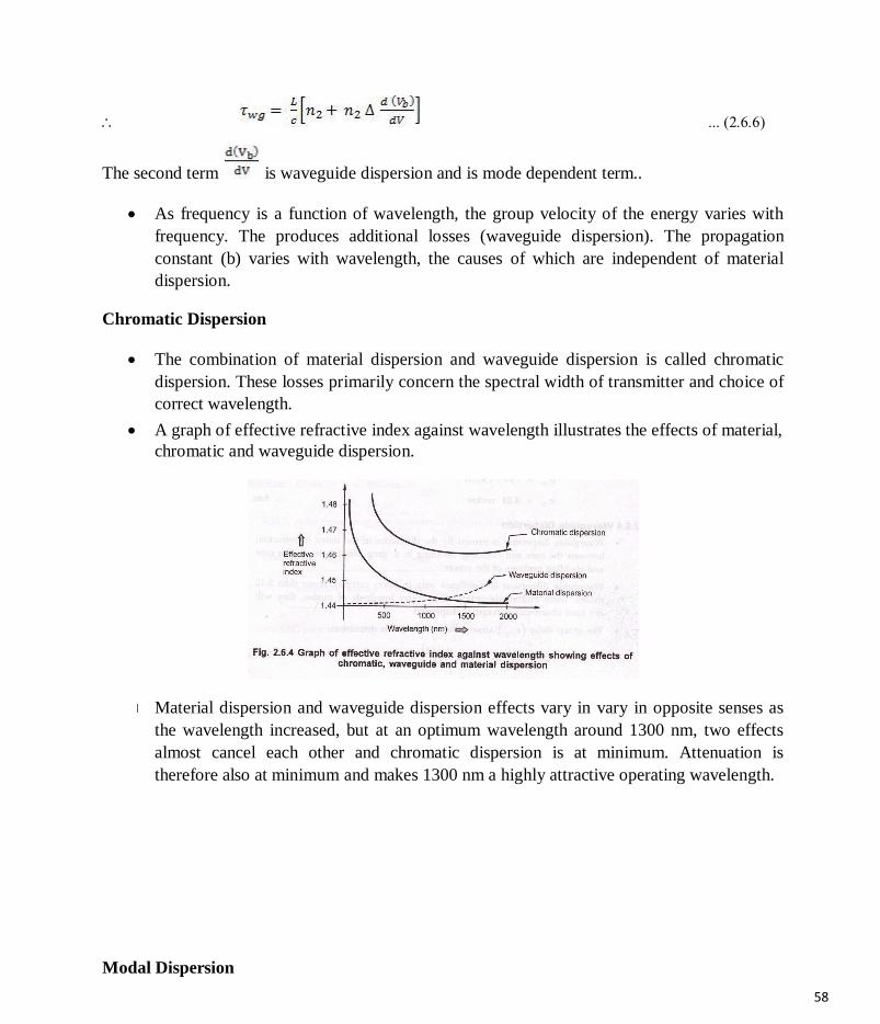
Chromatic Dispersion
The combination of material dispersion and waveguide dispersion is called chromatic
dispersion. These losses primarily concern the spectral width of transmitter and choice of
correct wavelength.
A graph of effective refractive index against wavelength illustrates the effects of material,
chromatic and waveguide dispersion.
Material dispersion and waveguide dispersion effects vary in vary in opposite senses as
the wavelength increased, but at an optimum wavelength around 1300 nm, two effects
almost cancel each other and chromatic dispersion is at minimum. Attenuation is
therefore also at minimum and makes 1300 nm a highly attractive operating wavelength.
Modal Dispersion

59
As only a certain number of modes can propagate down the fiber, each of these modes
carries the modulation signal and each one is incident on the boundary at a different
angle, they will each have their own individual propagation times. The net effect is
spreading of pulse, this form o dispersion is called modal dispersion.
Modal dispersion takes place in multimode fibers. It is moderately present in graded
index fibers and almost eliminated in single mode step index fibers. Modal dispersion is given by,
where ∆tmodal = Dispersion
n1 = Core refractive index
Z = Total fiber length
c = Velocity of light in air
= Fractional refractive index
Putting in above equation
The modal dispersion ∆tmodal describes the optical pulse spreading due to modal effects
optical pulse width can be converted to electrical rise time through the relationship.
Signal distortion in Single Mode Fibers
The pulse spreading σwg over range of wavelengths can be obtained from derivative of
group delay with respect t

60
where,
… (2.6.8)
This is the equation for waveguide dispersion for unit length.
Example 2.6.3 : For a single mode fiber n2 = 1.48 and = 0.2 % operating at A = 1320 nm,
compute the waveguide dispersion if
Solution : n2 = 1.48
0.2
= 1320 nm
Waveguide dispersion is given by,
i) -1.943 picosec/nm . km.
Higher Order Dispersion
Higher order dispersive effective effects are governed by dispersion slope S.
where, D is total dispersion
Also,
where,
β2 and β3 are second and third order dispersion parameters.
Dispersion slope S plays an important role in designing WDM system

61
Dispersion Induced Limitations
The extent of pulse broadening depends on the width and the shape of input pulses. The
pulse broadening is studied with the help of wave equation.
Basic Propagation Equation
The basic propagation equation which governs pulse evolution in a single mode fiber is
given by,
where,
β1, β2 and β3 are different dispersion parameters.
Chirped Gaussian Pulses
A pulse is said to b e chirped if its carrier frequency changes with time.
For a Gaussian spectrum having spectral width σω, the pulse broadening factor is given
by,
where, Vω = 2σω σ0
Limitations of Bit Rate
The limiting bit rate is given by,
4B σ ≤ 1
The condition relating bit rate-distance product (BL) and dispersion (D) is given

62
where, S is dispersion slope.
Limiting bit rate a single mode fibers as a function of fiber length for σλ = 0, a and 5nm is
shown in fig. 2.6.5.
Polarization Mode Dispersion (PMD)
Different frequency component of a pulse acquires different polarization state (such as
linear polarization and circular polarization). This results in pulse broadening is know as
polarization mode dispersion (PMD).
PMD is the limiting factor for optical communication system at high data rates. The
effects of PMD must be compensated.
2.7 Pulse Broadening in GI Fibers
The core refractive index varies radially in case of graded index fibers, hence it supports
multimode propagation with a low intermodal delay distortion and high data rate over
long distance is possible. The higher order modes travelling in outer regions of the core,
will travel faster than the lower order modes travelling in high refractive index region. If
the index profile is carefully controlled, then the transit times of the individual modes
will be identical, so eliminating modal dispersion. The r.m.s pulse broadening is given as:

63
… (2.7.1)
where,
σintermodal – R.M.S pulse width due to intermodal delay distortion.
σintermodal – R.M.S pulse width resulting from pulse broadening within each mode.
The intermodal delay and pulse broadening are related by expression given by Personick.
… (2.7.2)
Where τg is group delay.
From this the expression for intermodal pulse broadening is given as:
… (2.7.3)
The intramodal pulse broadening is given as :
… (2.7.4)
Where σλ is spectral width of optical source.
Solving the expression gives :

64
2.8 Mode Coupling
After certain initial length, the pulse distortion increases less rapidly because of mode
coupling. The energy from one mode is coupled to other mods because of: Structural imperfections. Fiber diameter variations. Refractive index variations. Microbends in cable.
Due to the mode coupling, average propagation delay become less and intermodal
distortion reduces.
Suppose certain initial coupling length = Lc, mode coupling length, over Lc = Z.
Additional loss associated with mode coupling = h (dB/ km).
Therefore the excess attenuation resulting from mode coupling = hZ.
The improvement in pulse spreading by mode coupling is given as :
where, C is constant independent of all dimensional quantities and refractive indices.
σc is pulse broadening under mode coupling.
σ0 is pulse broadening in absence of mode coupling.
For long fiber length’s the effect of mode coupling on pulse distortion is significant. For a
graded index fiber, the effect of distance on pulse broading for various coupling losses
are shown

65
Significant mode coupling occurs of connectors, splices and with other passive
components of an optical link.
2.9 Design Optimization
Features of single mode fibers are : Longer life. Low attenuation. Signal transfer quality is good. Modal noise is absent. Largest BW-distance product.
Basic design – optimization includes the following : Cut-off wavelength. Dispersion. Mode field diameter. Bending loss. Refractive index profile.
Refractive Index Profile
Dispersion of single mode silica fiber is lowest at 1300 nm while its attenuation is
minimum at 1550 nm. For archiving maximum transmission distance the dispersion null
should be at the wavelength of minimum attenuation. The waveguide dispersion is easier
to control than the material dispersion. Therefore a variety of core-cladding refractive.
idex configuration fivers. Such as 1300 nm – optimized fibers, dispersion shifted fibers,
dispersion – flattened fibers and large effective core area fibers.
1300 nm – Optimized Fibers
These are most popularly used fibers. The two configurations of 1300 nm – optimized
single mode fibers are :

66
Matched cladding fibers. Dressed cladding fibers.
Matched cladding fibers have uniform refractive index throughout its cladding. Typical
diameter is 9.0 µm and ∆ = 0.35 %.
Dressed cladding fibers have the innermost cladding portion has low refractive index than
outrcladding region. Typical diameter is 8.4 µm and ∆1 = 0.25 %, ∆2 = 0.12 %.
Fig 2.9.1 shows both types of fibers.
2. Dispersion Shifted Fibers
3. The addition of wavelength and material dispersion can shift the zero dispersion point of
longer wavelength. Two configurations of dispersion shifted fibers are
Step index dispersion shifted fiber. Triangular dispersion shifted fiber.
Dispersion Flattened

67
Dispersion flattened fibers are more complex to design. It offers much broader span of
wavelengths to suit desirable characteristics. Two configurations are :
Fig 2.9.4 shows total resultant dispersion.
Dispersion Calculations
The total dispersion consists of material and waveguide dispersions. The resultant
intermodal dispersion is given as,
where, τ is group delay per unit length of fiber.
The broadening σ of an optical pulse is given
σ = D (λ) Lσ λ

68
where, σλ is half power spectral width of source.
As the dispersion varies with wavelength and fiber type. Different formulae are used to
calculate dispersions for variety of fiber at different wavelength.
For a non – dispersion shifted fiber between 1270 nm to 1340 nm wavelength, the
expression for dispersion is given as :
where,
λ0 is zero dispersion wavelength.
S0 is value at dispersion slop at λ0.
Fig 2.9.5 shows dispersion performance curve for non-dispersion shifted fibers in 1270 –
1340 nm region.

69
Maximum dispersion specified as 3.5 ps/(nm . km) marked as dotted line in Fig. 2.9.5. The cut-off frequency of an optical fiber
The cut-off frequency of an optical fiber is determined not only by the fiber itself (modal
dispersion in case of multimode fibers and waveguide dispersion in case of single mode
fibers) but also by the amount of material dispersion caused by the spectral width of
transmitter.
Bending Loss Limitations
The macrobending and microbending losses are significant in single mode fibers at 1550
nm region, the lower cut-off wavelengths affects more. Fig. 2.9.6 shows macrobending
losses.
The bending losses are function of mode-filed diameter, smaller the mode-field diameter,
the smaller the bending loss. Fig. 2.9.7 shows loss due to mode-field diameter.
The bending losses are also function of bend-radius of curvature. If the bend radius is
less, the losses are more and when the radius is more, the bending losses are less.

70
Recommended Questions:
d) Briefly explain material dispersion with suitable sketch.
e) Give expression of pulse broadening in graded index fiber.
f) State the significance of mode coupling in optic fiber communication.
g) Explain in detail the design optimization of single mode fibers.
h) Elaborate dispersion mechanism in optical fibers.
UNIT - 3
OPTICAL SOURCES AND COUPLING
3.1 Optical Sources
Optical transmitter coverts electrical input signal into corresponding optical signal. The
optical signal is then launched into the fiber. Optical source is the major component in an
optical transmitter.
Popularly used optical transmitters are Light Emitting Diode (LED) and semiconductor
Laser Diodes (LD).
Characteristics of Light Source of Communication
To be useful in an optical link, a light source needs the following characteristics:
It must be possible to operate the device continuously at a variety of temperatures
for many years. It must be possible to modulate the light output over a wide range of modulating
frequencies. For fiber links, the wavelength of the output should coincide with one of transmission
windows for the fiber type used. To couple large amount of power into an optical fiber, the emitting area should be small. To reduce material dispersion in an optical fiber link, the output spectrum should
be narrow. The power requirement for its operation must be low.

71
The light source must be compatible with the modern solid state devices. The optical output power must be directly modulated by varying the input current
to the device. Better linearity of prevent harmonics and intermodulation distortion. High coupling efficiency. High optical output power. High reliability. Low weight and low cost.
Two types of light sources used in fiber optics are light emitting diodes (LEDs) and laser
diodes (LDs).
Light Emitting Diodes(LEDs)
p-n Junction
Conventional p-n junction is called as homojunction as same semiconductor material is
sued on both sides junction. The electron-hole recombination occurs in relatively
layer = 10 µm. As the carriers are not confined to the immediate vicinity of junction,
hence high current densities can not be realized.
The carrier confinement problem can be resolved by sandwiching a thin layer ( = 0.1 µm)
between p-type and n-type layers. The middle layer may or may not be doped. The carrier
confinement occurs due to bandgap discontinuity of the junction. Such a junction is call
heterojunction and the device is called double heterostructure. In any optical communication system when the requirements is –
1. Bit rate f 100-2—Mb/sec. 2. Optical power in tens of micro watts.
LEDs are best suitable optical source.
LED Structures
Heterojuncitons
A heterojunction is an interface between two adjoining single crystal
semiconductors with different bandgap. Heterojuctions are of two types, Isotype (n-n or p-p) or Antisotype (p-n).

72
Double Heterojunctions (DH)
In order to achieve efficient confinement of emitted radiation double heterojunctions are
used in LED structure. A heterojunciton is a junction formed by dissimilar semiconductors.
Double heterojunction (DH) is formed by two different semiconductors on each side of active
region. Fig. 3.1.1 shows double heterojunction (DH) light emitter.
The crosshatched regions represent the energy levels of freecharge. Recombination
occurs only in active InGaAsP layer. The two materials have different bandgap energies
and different refractive indices. The changes in bandgap energies create potential barrier
for both holes and electrons. The free charges can recombine only in narrow, well defined
active layer side.
A double heterjuction (DH) structure will confine both hole and electrons to a narrow
active layer. Under forward bias, there will be a large number of carriers injected into
active region where they are efficiently confined. Carrier recombination occurs in small
active region so leading to an efficient device. Antoer advantage DH structure is that the
active region has a higher refractive index than the materials on either side, hence light
emission occurs in an optical waveguide, which serves to narrow the output beam.
LED configurations
At present there are two main types of LED used in optical fiber links – Surface emitting LED. Edge emitting LED.
Both devices used a DH structure to constrain the carriers and the light to an
active layer.
Surface Emitting LEDs

73
In surface emitting LEDs the plane of active light emitting region is oriented
perpendicularly to the axis of the fiber. A DH diode is grown on an N-type substrate at the top of the diode
as shown in Fig. 3.1.2. A circular well is etched through the substrate of the device. A fiber is then
connected to accept the emitted
At the back of device is a gold heat sink. The current flows through the p-type material
and forms the small circular active region resulting in the intense beam of light.Diameter of circular active area = 50 µm Thickness of circular active area = 2.5 µm
Current density = 2000 A/cm2 half-power
Emission pattern = Isotropic, 120o beamwidth.
The isotropic emission pattern from surface emitting LED is of Lambartian pattern. In
Lambartian pattern, the emitting surface is uniformly bright, but its projected area
diminishes as cos θ, where θ is the angle between the viewing direction and the normal to
the surface as shown in Fig. 3.1.3. The beam intensity is maximum along the normal.
The power is reduced to 50% of its peak when θ = 60o, therefore the total half-power
beamwidth is 120o. The radiation pattern decides the coupling efficiency of LED.
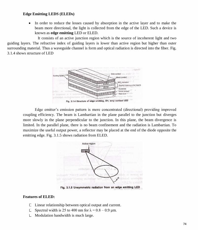
74
Edge Emitting LEDS (ELEDs)
In order to reduce the losses caused by absorption in the active layer and to make the
beam more directional, the light is collected from the edge of the LED. Such a device is
known as edge emitting LED or ELED.
It consists of an active junction region which is the source of incoherent light and two
guiding layers. The refractive index of guiding layers is lower than active region but higher than outer
surrounding material. Thus a waveguide channel is form and optical radiation is directed into the fiber. Fig.
3.1.4 shows structure of LED
Edge emitter’s emission pattern is more concentrated (directional) providing improved
coupling efficiency. The beam is Lambartian in the plane parallel to the junction but diverges
more slowly in the plane perpendicular to the junction. In this plane, the beam divergence is
limited. In the parallel plane, there is no beam confinement and the radiation is Lambartian. To
maximize the useful output power, a reflector may be placed at the end of the diode opposite the
emitting edge. Fig. 3.1.5 shows radiation from ELED.
Features of ELED:
Linear relationship between optical output and current. Spectral width is 25 to 400 nm for λ = 0.8 – 0.9 µm. Modulation bandwidth is much large.

75
Not affected by catastrophic gradation mechanisms hence are more reliable. ELEDs have better coupling efficiency than surface emitter. ELEDs are temperature sensitive.
Usage :
7. LEDs are suited for short range narrow and medium bandwidth links. 8. Suitable for digital systems up to 140 Mb/sec. 9. Long distance analog links
Light Source Materials
The spontaneous emission due to carrier recombination is called electro luminescence.
To encourage electroluminescence it is necessary to select as appropriate semiconductor
material. The semiconductors depending on energy bandgap can be categorized into, Direct bandgap semiconductors. Indirect bandgap semiconductors.
Some commonly used bandgap semiconductors are shown in following table 3.1.1
Semiconductor Energy bandgap (eV) Recombination Br (cm3 / sec)
GaAs Direct : 1.43 7.21 x 10⁻¹⁰
GaSb Direct : 0.73 2.39 x 10⁻¹⁰
InAs Direct : 0.35 8.5 x 10⁻¹¹
InSb Direct : 0.18 4.58 x 10⁻¹¹
Si Indirect : 1.12 1.79 x 10⁻¹⁵
Ge Indirect : 0.67 5.25 x 10⁻¹⁴
GaP Indirect : 2.26 5.37 x 10⁻¹⁴
Table 3.1.1 Semiconductor material for optical sources
Direct bandgap semiconductors are most useful for this purpose. In direct bandgap
semiconductors the electrons and holes on either side of bandgap have same value ofcrystal momentum. Hence direct recombination is possible. The recombination occurs
within 10-8
to 10-10
sec. In indirect bandgap semiconductors, the maximum and minimum energies occur at

76
different values of crystal momentum. The recombination in these semiconductors is
quite slow i.e. 10-2
and 10-3
sec. The active layer semiconductor material must have a direct bandgap. In direct bandgap
semiconductor, electrons and holes can recombine directly without need of third particle to conserve
momentum. In these materials the optical radiation is sufficiently high. these
materials are compounds of group III elements (Al, Ga, In) and group V element (P, As,
Sb). Some tertiary allos Ga1-x Alx As are also used.
Emission spectrum of Ga1-x AlxAs LED is shown in Fig. 3.1.6.
The peak output power is obtained at 810 nm. The width of emission spectrum at half
power (0.5) is referred as full width half maximum (FWHM) spectral width. For the
given LED FWHM is 36 nm.
The fundamental quantum mechanical relationship between gap energy E and frequency
v is given as –
where, energy (E) is in joules and wavelength (λ) is in meters. Expressing the gap energy
(Eg) in electron volts and wavelength (λ) in micrometers for this application.

77
Different materials and alloys have different band gap energies
The bandgap energy (Eg) can be controlled by two compositional parameters x and y,
within direct bandgap region. The quartenary alloy In1-x Gax Asy P1-y is the principal
material sued in such LEDs. Two expression relating Eg and x,y are –
… 3.1.3
… 3.1.4
Example 3.1.1 : Compute the emitted wavelength from an optical source having x = 0.07.
Solution : x = 0.07
Eg = 1.513 eV
Now
…Ans.
Example 3.1.2 : For an alloy In0.74 Ga0.26 As0.57 P0.43 to be sued in Led. Find the wavelength
emitted by this source.
Solution : Comparing the alloy with the quartenary alloy composition.
In1-x Gax As P1-y it is found that
x = 0.26 and y= 0.57

78
Eg = 1.35 – 0.72 y + 0.12 y2
Using
Eg = 1.35-(0.72 x 0.57) + 0.12 x 0.572
Eg = 0.978 eV
Now
… Ans.
Quantum Efficiency and Power
The internal quantum efficiency (ηint) is defined as the ratio of radiative recombination
rate to the total recombination rate.
… 3.1.5
Where,
Rr is radiative recombination rate.
Rnr is non-radiative recombination rate.
If n are the excess carriers, then radiative life time, and
non-radiative life time,
The internal quantum efficiency is given
The recombination time of carriers in active region is τ. It is also known as bulk
recombination life time.
… 3.1.7

79
Therefore internal quantum efficiency is given as –
… 3.1.8
If the current injected into the LED is I and q is electron charge then total number of
recombinations per second is –
From equation 3.1.5
Optical power generated internally in LED is given as –
Not all internally generated photons will available from output of device. The external
quantum efficiency is used to calculate the emitted power. The external quantum
efficiency is defined as the ratio of photons emitted from LED to the number of photons
generated internally. It is given by equation
… 3.1.11

80
The optical output power emitted from LED is given as –
Example 3.1.3 : The radiative and non radiative recombination life times of minority carriers in
the active region of a double heterojunction LED are 60 nsec and 90 nsec respectively.
Determine the total carrier recombination life time and optical power generated internally if the
peak emission wavelength si 870 nm and the drive currect is 40 mA. [July/Aug.-2006, 6 Marks]
Solutions : Given : λ = 870 nm 0.87 x 10⁻⁶
m
τr = 60 nsec.
τnr = 90 nsec.
I = 40 mA = 0.04 Amp.
i) Total carrier recombination life time:
τ nsec. … Ans.
ii) Internal optical power
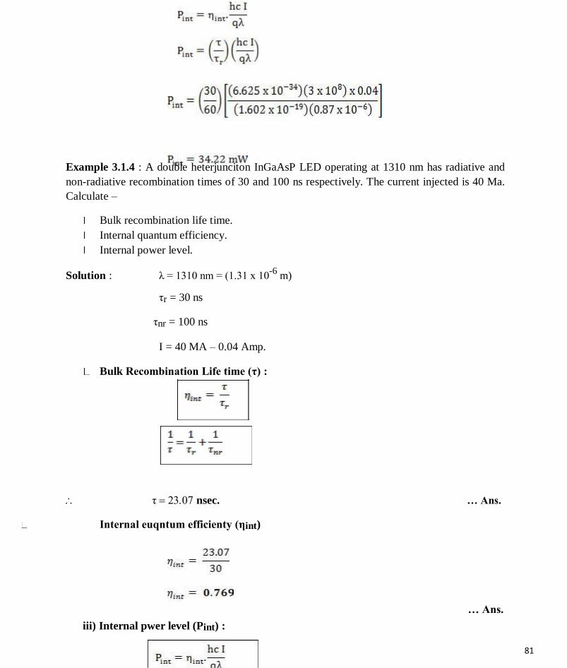
81
Example 3.1.4 : A double heterjunciton InGaAsP LED operating at 1310 nm has radiative and
non-radiative recombination times of 30 and 100 ns respectively. The current injected is 40 Ma.
Calculate –
Bulk recombination life time. Internal quantum efficiency. Internal power level.
Solution : λ = 1310 nm = (1.31 x 10⁻⁶
m)
τr = 30 ns
τnr = 100 ns
I = 40 MA – 0.04 Amp.
Bulk Recombination Life time (τ) :
τ nsec. … Ans.
Internal euqntum efficienty (ηint)
… Ans.
iii) Internal pwer level (Pint) :

82
Advantages and Disadvantages of LED
Advantages of LED
Simple design. Ease of manufacture. Simple system integration. Low cost. High reliability.
Disadvantages of LED
Refraction of light at semiconductor/air interface. The average life time of a radiative recombination is only a few nanoseconds, therefore
nodulation BW is limited to only few hundred megahertz. Low coupling efficiency. Large chromatic dispersion.
Comparison of Surface and Edge Emitting LED
Maximum Fiber coupled power
LED type modulation Output power (mW) (mW)
frequency (MHz)
Surface emitting 60 < 4 < 0.2
Edge emitting 200 < 7 < 1.0
Injection Laser Diode (ILD)
The laser is a device which amplifies the light, hence the LASER is an acronym for light
amplification by stimulated emission of radiation.The operation of the device may be described by the formation of an electromagnetic
standing wave within a cavity (optical resonator) which provides an output of
monochromatic highly coherent radiation.
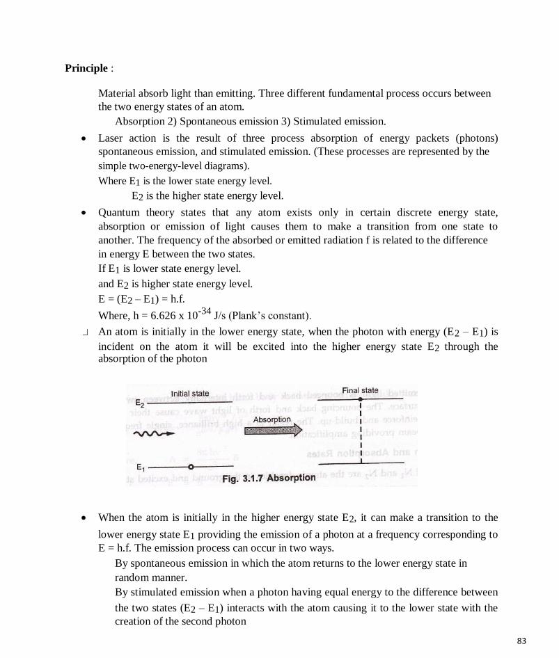
83
Principle :
Material absorb light than emitting. Three different fundamental process occurs between
the two energy states of an atom. Absorption 2) Spontaneous emission 3) Stimulated emission.
Laser action is the result of three process absorption of energy packets (photons)
spontaneous emission, and stimulated emission. (These processes are represented by thesimple two-energy-level diagrams).
Where E1 is the lower state energy level.
E2 is the higher state energy level.
Quantum theory states that any atom exists only in certain discrete energy state,
absorption or emission of light causes them to make a transition from one state to
another. The frequency of the absorbed or emitted radiation f is related to the differencein energy E between the two states.
If E1 is lower state energy level.
and E2 is higher state energy level.
E = (E2 – E1) = h.f.
Where, h = 6.626 x 10⁻³⁴
J/s (Plank’s constant). An atom is initially in the lower energy state, when the photon with energy (E2 – E1) is
incident on the atom it will be excited into the higher energy state E2 through the absorption of the photon
When the atom is initially in the higher energy state E2, it can make a transition to the
lower energy state E1 providing the emission of a photon at a frequency corresponding to
E = h.f. The emission process can occur in two ways. By spontaneous emission in which the atom returns to the lower energy state in
random manner. By stimulated emission when a photon having equal energy to the difference between
the two states (E2 – E1) interacts with the atom causing it to the lower state with the
creation of the second photon

84
Spontaneous emission gives incoherent radiation while stimulated emission gives
coherent radiation. Hence the light associated with emitted photon is of same frequency
of incident photon, and in same phase with same polarization.
It means that when an atom is stimulated to emit light energy by an incident wave, the
liberated energy can add to the wave in constructive manner. The emitted light is
bounced back and forth internally between two reflecting surface. The bouncing back and
forth of light wave cause their intensity to reinforce and build-up. The result in a high
brilliance, single frequency light beam providing amplification.
Emission and Absorption Rates
It N1 and N2 are the atomic densities in the ground and excited states.
Rate of spontaneous emission
Rspon = AN2 … 3.1.13
Rate of stimulated emission
Rstim = BN2 ρem … 3.1.14
Rate of absorption
Rabs = B’ N1 ρem … 3.1.15
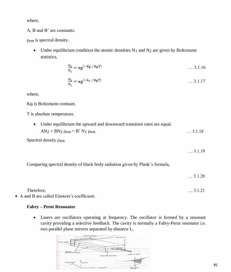
85
where,
A, B and B’ are constants.
ρem is spectral density.
Under equilibrium condition the atomic densities N1 and N2 are given by Boltzmann
statistics.
… 3.1.16
… 3.1.17
where,
KB is Boltzmann constant.
T is absolute temperature.
Under equilibrium the upward and downward transition rates are equal.
AN2 + BN2 ρem = B’ N1 ρem … 3.1.18
Spectral density ρem
… 3.1.19
Comparing spectral density of black body radiation given by Plank’s formula,
… 3.1.20
Therefore, … 3.1.21
A and B are called Einstein’s coefficient.
Fabry – Perot Resonator
Lasers are oscillators operating at frequency. The oscillator is formed by a resonant
cavity providing a selective feedback. The cavity is normally a Fabry-Perot resonator i.e.
two parallel plane mirrors separated by distance L,

86
Light propagating along the axis of the interferometer is reflected by the mirrors back to the
amplifying medium providing optical gain. The dimensions of cavity are 25-500 µm longitudinal
5-15 µm lateral and 0.1-0.2 µm transverse. Fig. 3.1.10 shows Fabry-Perot resonator cavity for a
laser diode.
The two heterojunctions provide carrier and optical confinement in a direction normal to
the junction. The current at which lasing starts is the threshold current. Above this current
the output power increases sharply.
Distributed Feedback (DFB) Laser
In DFB laster the lasing action is obtained by periodic variations of refractive index along
the longitudinal dimension of the diode. Fig. 3.1.11 shows the structure of DFB laser diode
Lasing conditions and resonant Frequencies
The electromagnetic wave propagating in longitudinal direction is expressed as –
E(z, t) = I(z) ej(ω
t-β
z)
…3.1.23
where,
I(z) is optical field intensity.
is optical radian frequency.
β is propagation constant.

87
The fundamental expression for lasing in Fabry-Perot cavity is –
… 3.1.24
where,
is optical field confinement factor or the fraction of optical power in the active layer.
α is effective absorption coefficient of material.
g is gain coefficient.
h v is photon energy.
z is distance traverses along the lasing cavity.
The condition of lasing threshold is given as –
For amplitude : I (2L) = I (0)
For phase : e-j2β
L
= 1
Optical gain at threshold = Total loss in the cavity.
i.e. Γ gth = αt
Now the lasing expression is reduced to –
… 3.1.26
… 3.1.27
where,
Αend is mirror loss in lasing cavity.
An important condition for lasing to occur is that gain, g ≥ g th i.e. threshold gain.
Example 3.1.5 : Find the optical gain at threshold of a laser diode having following parametric
values – R1 = R2 = 0.32, α = 10cm-1
and L = 500 µm.

88
Solution : Optical gain in laser diode is given by –
… Ans.
Power Current Characteristics The output optic power versus forward input current characteristics is plotted in Fig.
3.1.12 for a typical laser diode. Below the threshold current (Ith) only spontaneous
emission is emitted hence there is small increase in optic power with drive current. at
threshold when lasing conditions are satisfied. The optical power increases sharply after
the lasing threshold because of stimulated emission.
The lasing threshold optical gain (gth) is related by threshold current density (Jth) for
stimulated emission by expression –
g th = β Jth … 3.1.28
where, β is constant for device structure.
Fig. 3.1.12 Power current characteristics
External Quantum Efficiency

89
The external quantum efficiency is defined as the number of photons emitted per electron
hole pair recombination above threshold point. The external quantum efficiency ηext is
given by –
… 3.1.29
where,
ηi = Internal quantum efficiency (0.6-0.7).
gth = Threshold gain.
α = Absorption coefficient
Typical value of ηext for standard semiconductor laser is ranging between 15-20 %.
Resonant Frequencies
At threshold lasing
2β L = 2π m
where, (propagation constant)
m is an integer.
m
Since c = vλ
Substituting λ in 3.1.30
=z… 3.1.31
Gain in any laser is a function of frequency. For a Gaussian output the gain and
frequency are related by expression –

90
… 3.1.32
where,
g(0) is maximum gain.
λ0 is center wavelength in spectrum.
is spectral width of the gain.The frequency spacing between the two successive modes is –
… 3.1.34
Optical Characteristics of LED and Laser
The output of laser diode depends on the drive current passing through it. At low drive
current, the laser operates as an inefficient Led, When drive current crosses threshold
value, lasing action beings. Fig. 3.1.13 illustrates graph comparing optical powers of
LED operation (due to spontaneous emission) and laser operation (due to stimulated
emission).
Spectral and Spatial Distribution of Led and Laser
At low current laser diode acts like normal LED above threshold current, stimulated
emission i.e. narrowing of light ray to a few spectral lines instead of broad spectral distribution, exist. This
enables the laser to easily couple to single mode fiber and reduces the amount of uncoupled light (i.e.
spatial radiation distribution). Fig. 3.1.14 shows spectral and spatial distribution difference between two
diodes

91
Advantages and Disadvantages of Laser Diode
Advantages of Laser Diode
Simple economic design. High optical power. Production of light can be precisely controlled. Can be used at high temperatures. Better modulation capability. High coupling efficiency. Low spectral width (3.5 nm) Ability to transmit optical output powers between 5 and 10 mW. Ability to maintain the intrinsic layer characteristics over long periods.
Disadvantages of Laser Diode
At the end of fiber, a speckle pattern appears as two coherent light beams add or subtract
their electric field depending upon their relative phases.
Laser diode is extremely sensitive to overload currents and at high transmission rates,
when laser is required to operate continuously the use of large drive current produces
unfavourable thermal characteristics and necessitates the use of cooling and power
stabilization.
Comparison of LED and Laser Diode
Sr. No. Parameter LED LD (Laser Diode)
1. Principle of operation Spontaneous emission. Stimulated emission.
2. Output beam Non – coherent. Coherent.
3. Spectral width Board spectrum (20 nm – 100 nm) Much narrower (1-5 nm).

92
4. Data rate Low. Very high.
5. Transmission distance Smaller. Greater.
6. Temperature sensitivity Less sensitive. More temperature sensitive.
7. Coupling efficiency Very low. High.
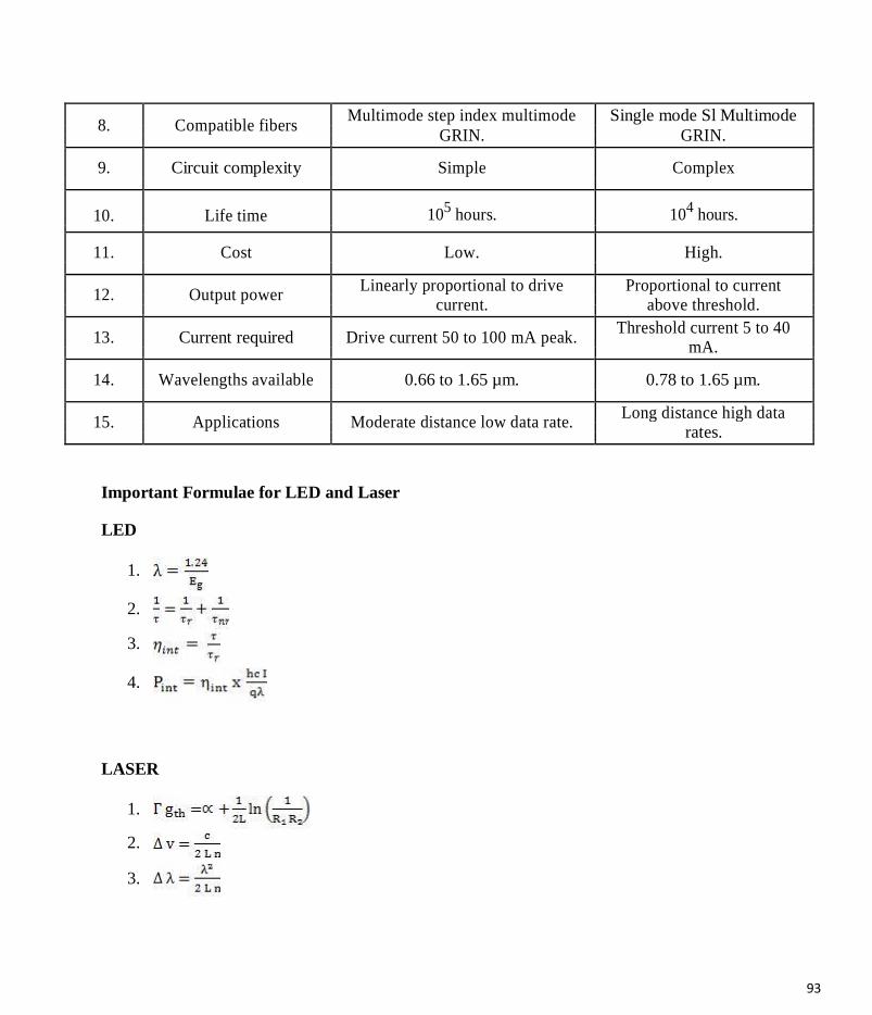
93
8. Compatible fibers Multimode step index multimode Single mode Sl Multimode
GRIN. GRIN.
9. Circuit complexity Simple Complex
10. Life time 105 hours. 10
4 hours.
11. Cost Low. High.
12. Output power Linearly proportional to drive Proportional to current
current. above threshold.
13. Current required Drive current 50 to 100 mA peak. Threshold current 5 to 40
mA.
14. Wavelengths available 0.66 to 1.65 µm. 0.78 to 1.65 µm.
15. Applications Moderate distance low data rate. Long distance high data
rates.
Important Formulae for LED and Laser
LED
1.
2.
3.
4.
LASER
1.
2.
3.

94
3.2 Optical Detectors
Principles of Optical Detectors
The photodetector works on the principle of optical absorption. The main requirement of
light detector or photodector is its fast response. For fiber optic communication purpose
most suited photodetectors are PIN (p-type- Instrinsic-n-type) diodes and APD
(Avalanche photodiodes)
The performance parameters of a photodetector are responsivity, quantum efficiency,
response time and dark current.
Cut-off Wavelength (λc)
Any particular semiconductor can absorb photon over a limited wavelength range. The
highest wavelength is known as cut-off wavelength (λc). The cut-off wavelength is
determined by bandgap energy Eg of material.
… 3.2.1
where,
Eg inelectron volts (eV) and
λc cut-off wavelength is in µm.
Typical value of λc for silicon is 1.06 µm and for germanium it is 1.6 µm.
Quantum Efficiency (η)
The quantum efficiency is define as the number of electron-hole carrier pair generated
per incident photon of energy h v and is given as –
… 3.2.2
where, Ip is average photocurrent.
Pin is average optical power incident on photo detectors.

95
Absorption coefficient of material determines the quantum efficiency. Quantum
efficiency η < 1 as all the photons incident will not generate e-h pairs. It is normally
expressed in percentage.
Fiber Alignment
In any fiber optic communication system, in order to increase fiber length there is need to
joint the length of fiber. The interconnection of fiber causes some loss of optical power.
Different techniques are used to interconnect fibers. A permanent joint of cable is
referred to as splice and a temporary joint can be done with the connector.
The fraction of energy coupled from one fiber to other proportional to common mode
volume Mcommon. The fiber – to – fiber coupling efficiency is given as –
where,
ME is number of modes in fiber which launches power into next fiber.
The fiber – to – fiber coupling loss LF is given as –
LF = -10log ηF
Mechanical Misalignment
The diameter of fiber is few micrometer hence the microscopic alignment is required. If the
radiation cone of emitting fiber does not match the acceptance cone of receiving fiber, radiation
loss takes place. The magnitude of radiation loss depends on the degree of misalignment.
Different types of mechanical misalignments are shown in Fig. 4.1.1.

96
Lateral misalignment
Lateral or axial misalignment occurs when the axes of two fibers are separated by
distance ‘d’.Longitudinal misalignment
Longitudinal misalignment occurs when fibers have same axes but their end faces are
separated by distance ‘S’.Angular misalignment Angular misalignment occurs when fiber axes and fiber end faces are no longer parallel.
There is an angle ‘θ’ between fiber end faces. The axial or lateral misalignment is most common in practice causing considerable power loss. The
axial offset reduces the common core area of two fiber end faces as shown in
The optical power coupled is proportional to common area of two fiber cores.
The common area is given by expression –
… (4.1.3)
where,

97
a is core radius of fiber.
d is separation of core axes.
The coupling efficiency for step index fiber is the ratio of common core area to the end-
face area.
For graded index fiber, the total received power for axial misalignment is given by –
.1.5)
where,
P is the power in emitting fiber.
When, d << a, the above expression reduces … (4.1.6)
Fiber Related Losses
Losses in fiber cables also causes due to differences in geometrical and
fiber characteristics.These includes, 1) Variation in core diameter. 2) Core area ellipticity. 3) Numerical aperture. 4) Refractive – index profile. 5) Core-cladding concentricity.
The user have less control over these variations since they are related to
manufacturing process.

98
Coupling loss when emitter fiber radius aE and receiving fiber radius aR is not same,
is given as –
(4.1.7)
where,
aE is emitter fiber radius.
aR is receiver fiber radius.
Coupling loss when numerical apertures of two fibers are not equal, to expressed as –
(4.1.8)
Coupling loss when core refractive index of two fibers are not same, is expressed as
(4.1.9)
Fiber Splices
A permanent or semipermanent connection between two individual optical fibers is
known as fiber splice. And the process of joining two fibers is called as splicing.
Typically, a splice is used outside the buildings and connectors are used to join the cables
within the buildings. Splices offer lower attenuation and lower back reflection than
connectors and are less expensive.
Types of Splicing
There are two main types of splicing Fusion splicing. Mechanical splicing / V groove
Fusion Splicing
Fusion splicing involves butting two cleaned fiber end faces and heating them until they
melt together or fuse.
Fusion splicing is normally done with a fusion splicer that controls the alignment of the
two fibers to keep losses as low as 0.05 dB.

99
6. Fiber ends are first prealigned and butted together under a microscope with
micromanipulators. The butted joint is heated with electric arc or laser pulse to melt the fiber
ends so can be bonded together. Fig. 4.2.1 shows fusion splicing of optical fiber
Mechanical Splicing / V Groove
Mechanical splices join two fibers together by clamping them with a structure or by
epoxying the fibers together.
Mechanical splices may have a slightly higher loss and back reflection. These can be
reduced by inserting index matching gel.
V groove mechanical splicing provides a temporary joint i.e fibers can be disassembled if
required. The fiber ends are butted together in a V – shaped groove as shown in Fig..
The splice loss depends on fiber size and eccentricity.
Source-to-Fiber Power Launching

100
Optical output from a source is measured in radiance (B). Radiance is defined as the optical power
radiated into a solid angle per unit emitting surface area. Radiance is
specified in Watts/cm2/Steradian. Radiance is important for defining source to fiber
coupling efficiency.
Source Output Pattern
Spatial radiation pattern of source helps to determine the power accepting capability of
fiber.
Fig. 4.3.1 shows three dimensional spherical co-ordinate system for characterizing the
emission pattern from an optical source. Where the polar axis is normal to the emitting
surface and radiance is a function of θ and .
The Lambartian output by surface emitting LED is equally bright from any direction. The
emission pattern of Lambartian output is shown in Fig. 4.3.2 and its output is –
B(θ,) = B0cos θ
where, B0 is the radiance along the normal to the radiating surface.

101
Both radiations in parallel and normal to the emitting plane are approximated by
expression –
… (4.3.2)
where,
T and L are transverse and lateral power distribution coefficients.
Power Coupling Calculation
To calculate power coupling into the fiber, consider an optical source launched into the
fiber as shown in Fig. 4.3.3.
Brightness of source is expressed as B(As, Ωs),
Where, As is area of source
Ωs is solid emission angle of source.
The coupled power P can be calculated as –
… (4.3.3)

102
The integral limits are area of source and solid acceptance angle (θ0max).
Here dθs rdr is incremental emitting area.
Let the radius of surface emitting LED is rs, and for Lambartian emitter, B(θ,) = B0 cos
θ then
… (4.3.4)
Since
Power coupled to step – index fiver
For step index fiber NA is not dependent on θs and r. Therefore LED power from step
index fiber is,
… (4.3.5)
Consider optical power Ps emitted from source are As into hemisphere(2π Sr).
When source radius rs <a, the fiber core radius, the LED output power is given from
equation (4.3.5).
… (4.3.7)
When rs > a equation (4.3.5) becomes,
… (4.3.8)

103
Power coupled to graded index fiber
In graded index fiber, the index of refraction varies radially from fiber axis. Numerical
aperture for graded index fiber is given by,
Is source radius (rs) is less than fiber core radius (a) i.e. rs <a, the power coupled from surface
emitting LED is given as –
For coupling maximum power to fiber, the refractive index of the medium separating
source and fiber must be same, otherwise there will be loss of power. The power couple
is reduced by factor,
where,
n is the refractive index of medium.
n1 is the refractive index of fiber core. R is the Fresnel reflection or reflectivity
Lensing Schemes for Coupling Improvement
When When the emitting area of the source is smaller than the core area of fiber, the
power coupling efficiency becomes poor. In order to improve the coupling efficiency
miniature lens is placed between source and fiber. Microlens magnifies the emitting area
of source equal to core area. The power coupled increases by a factor equal to
magnification factor of lens.
Important types of lensing schemes are : Rounded – end fiber. Spherical – surfaced LED and Spherical-ended fiber. Taper ended fiber. Non imaging microsphere. Cylindrical lens, Imaging sphere.
There are some drawbacks of using lens.

104
Complexity increases. Fabrication and handling difficulty.
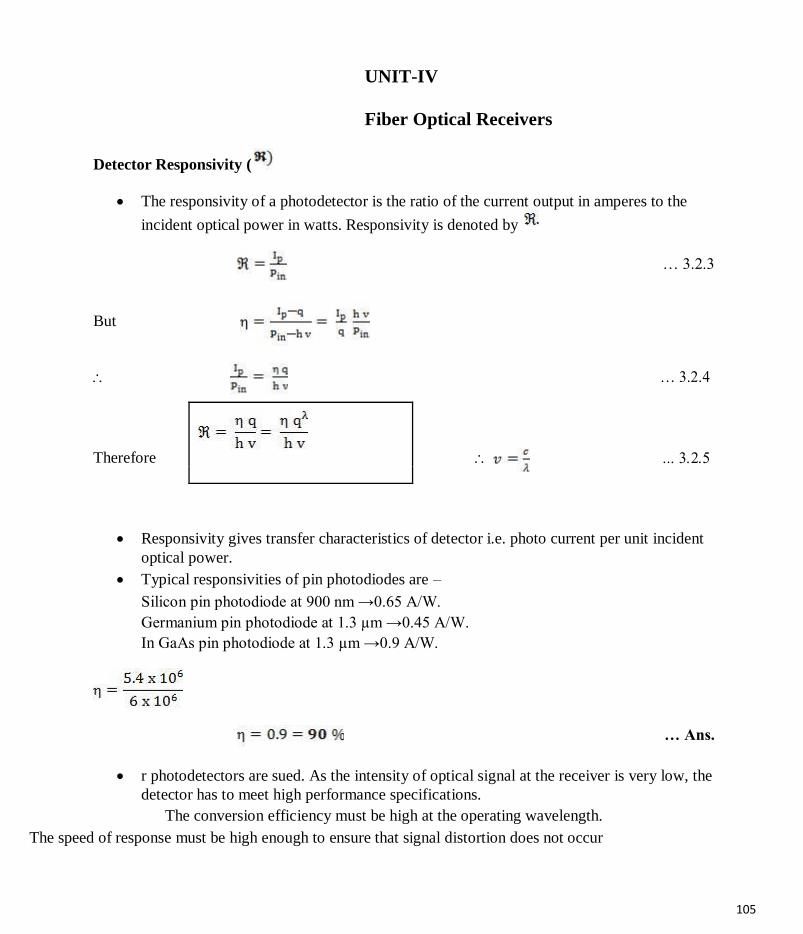
105
UNIT-IV
Fiber Optical Receivers
Detector Responsivity (
The responsivity of a photodetector is the ratio of the current output in amperes to the
incident optical power in watts. Responsivity is denoted by
… 3.2.3
But
… 3.2.4
Therefore
Responsivity gives transfer characteristics of detector i.e. photo current per unit incident
optical power. Typical responsivities of pin photodiodes are –
Silicon pin photodiode at 900 nm →0.65 A/W.
Germanium pin photodiode at 1.3 µm →0.45 A/W.
In GaAs pin photodiode at 1.3 µm →0.9 A/W.
… Ans.
r photodetectors are sued. As the intensity of optical signal at the receiver is very low, the
detector has to meet high performance specifications. The conversion efficiency must be high at the operating wavelength.
The speed of response must be high enough to ensure that signal distortion does not occur

106
The detection process introduce the minimum amount of noise. It must be possible to operate continuously over a wide range of temperatures for
many years. The detector size must be compatible with the fiber dimensions.
At present, these requirements are met by reverse biased p-n photodiodes. In these
devices, the semiconductor material absorbs a photon of light, which excites an electron
from the valence band to the conduction band (opposite of photon emission). The photo
generated electron leaves behind it a hole, and so each photon generates two charge
carriers. The increases the material conductivity so call photoconductivity resulting in an
increase in the diode current. The diode equation is modified as –
… 3.2.6
where,
Id is dark current i.e. current that flows when no signal is present.
Is is photo generated current due to incident optical signal.
Fig. 3.2.1 shows a plot of this equation for varying amounts of incident optical power.
Three regions can be seen forward bias, reverse bias and avalanche breakdown.Forward bias, region 1 : A change in incident power causes a change in terminal voltage, it
is called as photovoltaic mode. If the diode is operated in this mode, the frequency response of the
diode is poor and so photovoltaic operation is rarely used in optical links

107
Reverse bias, region 2 : A change in optical power produces a proportional
change in diode current, it is called as photoconductive mode of operation which most
detectors use. Under these condition, the exponential term in equation 3.2.6 becomes
insignificant and the reverse bias current is given by –
Responsivity of photodiode is defined as the change in reverse bias current per unit
change in optical powr, and so efficient detectors need large responsivities.
Avalanche breakdown, region 3 : When biased in this region, a photo generated
electron-hole pair causes avalanche breakdown, resulting in large diode for a single incident
photon. Avalance photodiodes (APDs) operate in this region APDs exhibit carrier
multiplication. They are usually very sensitive detectors. Unfortunately V-I characteristic is
very steep in this region and so the bias voltage must be tightly controlled to prevent
spontaneous breakdown.
PIN Photodiode
PIN diode consists of an intrinsic semiconductor sandwiched between two heavily doped
p-type and n-type semiconductors as shown in Fig. 3.2.2

108
Sufficient reverse voltage is applied so as to keep intrinsic region free
from carries, so its resistance is high, most of diode voltage appears
across it, and the electrical forces are strong within it. The incident
photons give up their energy and excite an electron from valance to
conduction band. Thus a free electron hole pair is generated, these are
as photocarriers. These carriers are collected across the reverse biased
junction resulting in rise in current in external circuit called photocurrent.
In the absence of light, PIN photodiodes behave electrically just like an
ordinary rectifier diode. If forward biased, they conduct large amount of
current
PIN detectors can be operated in two modes : Photovoltaic and
photoconductive. In photovoltaic mode, no bias is applied to the
detector. In this case the detector works very slow, and output is
approximately logarithmic to the input light level. Real world fiber optic
receivers never use the photovoltaic mode.
In photoconductive mode, the detector is reverse biased. The output in
this case is a current that is very linear with the input light power.
The intrinsic region some what improves the sensitivity of the device. It
does not provide internal gain. The combination of different
semiconductors operating at different wavelengths allows the selection of
material capable of responding to the desired operating wavelength.
Characteristics of common PIN photodiodes
Sr. No. Parameters Symbol Unit Si Ge InGaAs
1. Wavelength λ µ m 0.4 – 1.1 0.8 – 1.8 1.0 – 1.7
2. Reponsivity A/W 0.4 – 0.6 0.5 – 0.7 0.6 – 0.9
3. Quantum
Η % 75 -90 50 – 55 60 – 70 efficiency
4. Darl current Id nA 1 – 10 50 – 500 1 - 20
5. Rise time Tr nS 0.5 – 1 0.1 – 0.5 0.02 – 0.5
6. Bandwidth B GHz 0.3 – 0.6 0.5 – 3 1 – 10
7. Bias
Vb V 50 – 100 5 – 10 5 - 6 voltage
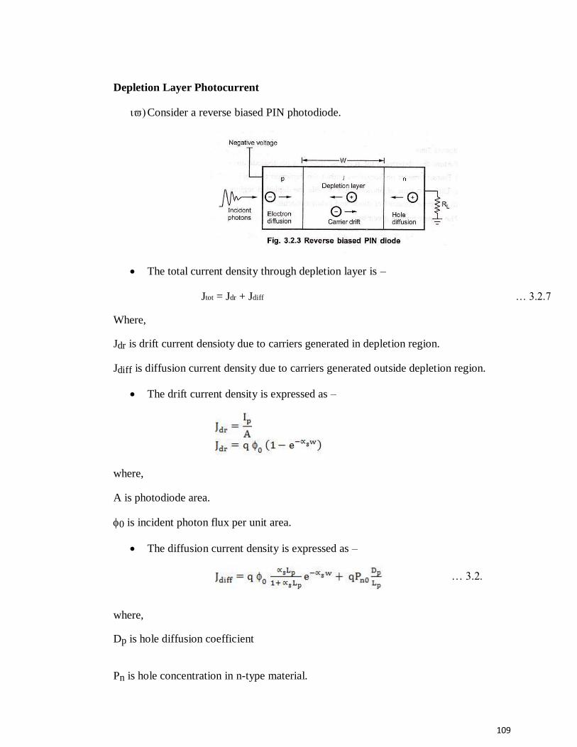
109
Depletion Layer Photocurrent
Consider a reverse biased PIN photodiode.
The total current density through depletion layer is –
Jtot = Jdr + Jdiff … 3.2.7
Where,
Jdr is drift current densioty due to carriers generated in depletion region.
Jdiff is diffusion current density due to carriers generated outside depletion region.
The drift current density is expressed as –
where,
A is photodiode area.
0 is incident photon flux per unit area.
The diffusion current density is expressed as –
… 3.2.
where,
Dp is hole diffusion coefficient
Pn is hole concentration in n-type material.

110
Pn0 is equilibrium hole density.
Substituting in equation 3.2.7, total current density through reverse biased
depletion layer
is –
Response Time
Factors that determine the response time of a photodiode are – Transit time of photocarriers within the depletion region. Diffusion time of photocarriers outside the depletion region. RC time constant of diode and external circuit.
The transit time is given by –
The diffusion process is slow and diffusion times are less than carrier
drift time. By considering the photodiode response time the effect of
diffusion can be calculated. Fig. 3.2.4 shows the response time of
photodiode which is not fully depleted.
The detector behaves as a simple low pass RC filter having passband of
where
RT, is combination input resistance of load and amplifier.
CT is sum of photodiode and amplifier capacitance.

111
Example 3.2.5 : Compute the bandwidth of a photodetector having parameters as –
Photodiode capacitance = 3 pF
Amplifier capacitance = 4 pF
Load resistance = 50 Ω
Amplifier input resistance = 1 MΩ
Solution : Sum of photodiode and amplifier capacitance
CT = 3 + 4 = 7 pF
Combination of load resistance and amplifier and input resistance
RT = 50Ω || 1 MΩ ≈ 50 Ω
B = 454.95 MHz … Ans.
Avalanche Photodiode (APD)
When a p-n junction diode is applied with high reverse bias breakdown
can occur by two separate mechanisms direct ionization of the lattice
atoms, zener breakdown and high velocity carriers impact ionization of
the lattice atoms called avalanche breakdown. APDs uses the avalanche
breakdown phenomena for its operation. The APD has its internal gain
which increases its responsivity.
Fig. 3.2.5 shows the schematic structure of an APD. By virtue of the
doping concentration and physical construction of the n+ p junction, the
electric filed is high enough to cause impact ionization. Under normal
operating bias, the I-layer (the p־ region) is completely depleted. This is
known as reach through condition, hence APDs are also known as
reach through APD or RAPDs
Similar to PIN photodiode, light absorption in APDs is most efficient in
I-layer. In this region, the E-field separates the carriers and the electrons
drift into the avalanche region where carrier multiplication occurs. If the
APD is biased close to breakdown, it will result

112
in reverse leakage current. Thus APDs are usually biased just below
breakdown, with the bias voltage being tightly controlled. The multiplication for all carriers generated in the photodiode is given as –
…
where,
IM = Average value of total multiplied output current.
IP = Primary unmultiplied photocurrent.
Responsivity of APD is given by –
…
where, 0 = Unity gain responsivity
MSM Photodetector
Metal-semiconductor-metal (MSM) photodetector uses a sandwiched
semiconductor between two metals. The middle semiconductor layer acts
as optical absorbing layer. A Schottky barrier is formed at each metal
semiconductor interface (junction), which prevents flow of electrons.
When optical power is incident on it, the electron-hole pairs generated
through photo absorption flow towards metal contacts and causes
photocurrent.
MSM photodetectors are manufactured using different combinations of
semiconductors such as – GaAs, InGaAs, InP, InAIAs. Each MSM
photodetectors had distinct features e.g. responsivity, quantum efficiency,
bandwidth etc.

113
With InAIAs based MSM photodetector, 92 % quantum efficiency can be
obtained at 1.3 µm with low dark current. An inverted MSM
photodetector shows high responsivity when illuminated from top. A GaAs based device with travelling wave structure gives a bandwidth beyond
500 GHz.
Optical Detector
With a proper sketch briefly explain the structure of PIN diode.
Explain the following term relating to PIN photodiode with proper expressions.
Cut-off wavelength.
Quantum efficiency.
Responsivity.
Explain the structure and principle of working of APD.
Deduce the expression for total current density for APD.
How the response time of APD is estimated?
Give expression for passband of APD detector.
Compare the performance parameters of PIN and APD.
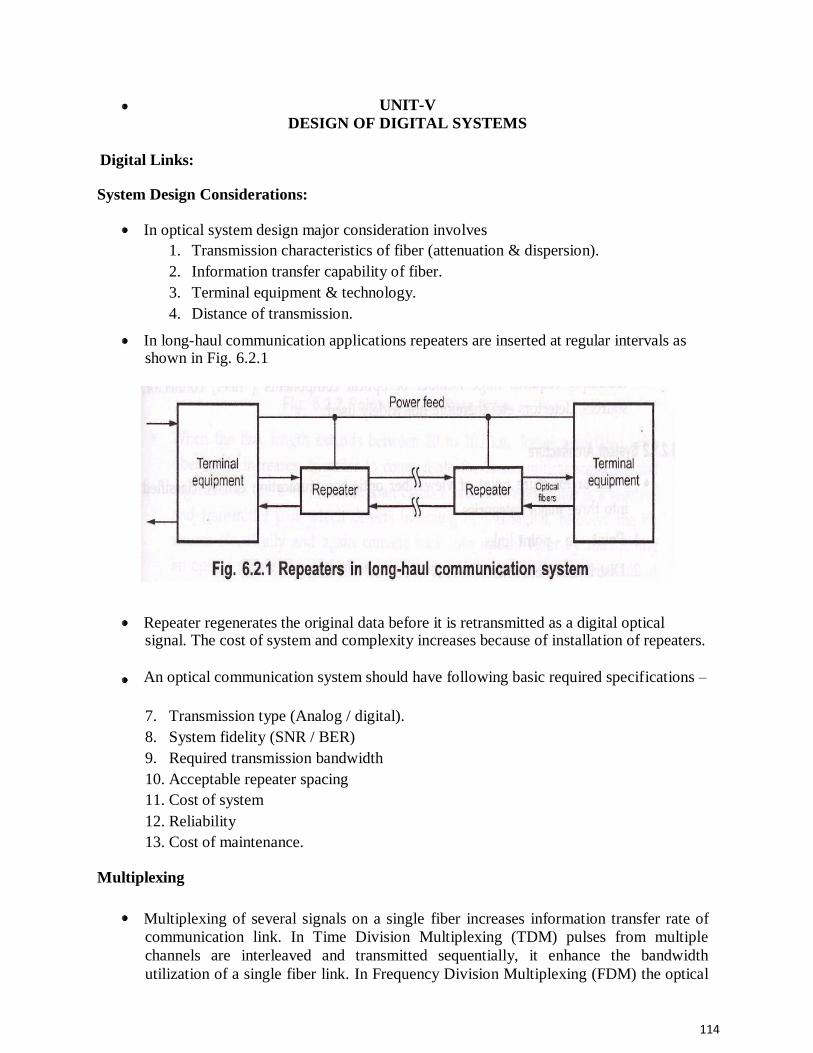
114
UNIT-V
DESIGN OF DIGITAL SYSTEMS
Digital Links: System Design Considerations:
In optical system design major consideration involves 1. Transmission characteristics of fiber (attenuation & dispersion). 2. Information transfer capability of fiber. 3. Terminal equipment & technology. 4. Distance of transmission.
In long-haul communication applications repeaters are inserted at regular intervals as shown in Fig. 6.2.1
Repeater regenerates the original data before it is retransmitted as a digital optical signal. The cost of system and complexity increases because of installation of repeaters.
An optical communication system should have following basic required specifications –
7. Transmission type (Analog / digital). 8. System fidelity (SNR / BER) 9. Required transmission bandwidth 10. Acceptable repeater spacing 11. Cost of system 12. Reliability 13. Cost of maintenance.
Multiplexing
Multiplexing of several signals on a single fiber increases information transfer rate of
communication link. In Time Division Multiplexing (TDM) pulses from multiple
channels are interleaved and transmitted sequentially, it enhance the bandwidth
utilization of a single fiber link. In Frequency Division Multiplexing (FDM) the optical

115
channel bandwidth is divided inot various nonoverlapping frequency bands and each
signal is assigned one of these bands of frequencies. By suitable filtering the combined
FDM signal can be retrieved. When number of optical sources operating at different wavelengths are to be sent on
single fiber link Wavelength Division Multiplexing (WDM) is used. At receiver end, the
separation or extraction of optical signal is performed by optical filters (interference
filters, differaction filters prism filters). Another technique called Space Division Multiplexing (SDM) used separate fiber within
fiber bundle for each signal channel. SDM provides better optical isolation which
eliminates cross-coupling between channels. But this technique requires huge number of
optical components (fiber, connector, sources, detectors etc) therefore not widely used.
System Architecture
From architecture point of view fiber optic communication can be classified into three major categories.
Point – to – point links Distributed networks Local area networks.
Point-to-Point Links:
A point-to-point link comprises of one transmitter and a receiver system. This is the
simplest form of optical communication link and it sets the basis for examining complex
optical communication links. For analyzing the performance of any link following important aspects are to be considered.
Distance of transmission Channel data rate Bit-error rate
All above parameters of transmission link are associated with the characteristics of
various devices employed in the link. Important components and their characteristics are
listed below. When the link length extends between 20 to 100 km, losses associated with fiber cable
increases. In order to compensate the losses optical amplifier and regenerators are used
over the span of fiber cable. A regenerator is a receiver and transmitter pair which
detects incoming optical signal, recovers the bit stream electrically and again convert
back into optical from by modulating an optical source. An optical amplifier amplify the
optical bit stream without converting it into electrical form. The spacing between two repeater or optical amplifier is called as repeater spacing (L).
The repeater spacing L depends on bit rate B. The bit rate-distance product (BL) is a
measure of system performance for point-to-point links.

116
Two important analysis for deciding performance of any fiber link are – Link power budget / Power budget Rise time budget / Bandwidth budget
The Link power budget analysis is used to determine whether the receiver has sufficient power to
achieve the desired signal quality. The power at receiver is the transmitted power minus link losses.
The components in the link must be switched fast enough and the fiber dispersion must be low
enough to meet the bandwidth requirements of the application. Adequate bandwidth for a system
can be assured by developing a rise time budget.
System Consideration:
Before selecting suitable components, the operating wavelength for the system is decided. The
operating wavelength selection depends on the distance and attenuation. For shorter distance, the
800-900 nm region is preferred but for longer distance 100 or 1550 nm region is preferred due to
lower attenuations and dispersion. The next step is selection of photodetector. While selecting a photodetector following factors are considered –
Minimum optical power that must fall on photodetector to satisfy BER at specified data rate. Complexity of circuit. Cost of design. Bias requirements.
Next step in system consideration is choosing a proper optical source, important factors to consider are –
Signal dispersion. Data rate. Transmission distance. Cost. Optical power coupling. Circuit complexity.
The last factor in system consideration is to selection of optical fiber between single mode and
multimode fiber with step or graded index fiber. Fiber selection depends on type of optical source
and tolerable dispersion. Some important factors for selection of fiber are : Numerical Aperture (NA), as NA increases, the fiber coupled power increases also the
dispersion. Attenuation characteristics. Environmental induced losses e.g. due to temperature variation, moisture and dust etc.