Embed Size (px)
Citation preview

Lecture Note
On
Microprocessor and Microcontroller
Theory and Applications
Subject Code:BEE-1501
Semester: 5th
Branch: EE and EEE

Syllabus

Disclaimer
This document does not claim any originality and cannot be used as a
substitute for prescribed textbooks. The information presented here is merely a
collection by the committee members for their respective teaching
assignments. Various sources as mentioned at the end of the document as well
as freely available material from internet were consulted for preparing this
document. The ownership of the information lies with the respective authors or
institutions. Further, this document is not intended to be used for commercial
purpose and the committee members are not accountable for any issues, legal,
or otherwise, arising out of this document. The committee members make no
representations or warranties with respect to the accuracy or completeness of
the contents of this document and specially disclaim any implied warranties of
merchantability or fitness for a particular purpose. The committee members
shall not be liable for any loss or profit or any other commercial damages,
including but not limited to special, incidental, consequential, or other
damages.

MODULE: 1
1. INTRODUCTION TO MICROPROCESSOR AND MICROCOMPUTER
ARCHITECTURE:
A microprocessor is a programmable electronics chip that has computing and decision
making capabilities similar to central processing unit of a computer. Any microprocessor-
based systems having limited number of resources are called microcomputers. Nowadays,
microprocessor can be seen in almost all types of electronics devices like mobile phones,
printers, washing machines etc. Microprocessors are also used in advanced applications like
radars, satellites and flights. Due to the rapid advancements in electronic industry and large
scale integration of devices results in a significant cost reduction and increase application of
microprocessors and their derivatives.
Fig.1 Microprocessor-based system
Bit: A bit is a single binary digit.
Word: A word refers to the basic data size or bit size that can be processed by the
arithmetic and logic unit of the processor. A 16-bit binary number is called a word in
a 16-bit processor.
Bus: A bus is a group of wires/lines that carry similar information.
System Bus: The system bus is a group of wires/lines used for communication
between the microprocessor and peripherals.
Memory Word: The number of bits that can be stored in a register or memory
element is called a memory word.
Address Bus: It carries the address, which is a unique binary pattern used to identify
a memory location or an I/O port. For example, an eight bit address bus has eight
lines and thus it can address 28 = 256 different locations. The locations in
hexadecimal format can be written as 00H – FFH.
Data Bus: The data bus is used to transfer data between memory and processor or
between I/O device and processor. For example, an 8-bit processor will generally
have an 8-bit data bus and a 16-bit processor will have 16-bit data bus.
Control Bus: The control bus carry control signals, which consists of signals for
selection of memory or I/O device from the given address, direction of data transfer
and synchronization of data transfer in case of slow devices.

A typical microprocessor consists of arithmetic and logic unit (ALU) in association with
control unit to process the instruction execution. Almost all the microprocessors are based
on the principle of store-program concept. In store-program concept, programs or
instructions are sequentially stored in the memory locations that are to be executed. To do
any task using a microprocessor, it is to be programmed by the user. So the programmer
must have idea about its internal resources, features and supported instructions. Each
microprocessor has a set of instructions, a list which is provided by the microprocessor
manufacturer. The instruction set of a microprocessor is provided in two forms: binary
machine code and mnemonics.
Microprocessor communicates and operates in binary numbers 0 and 1. The set of
instructions in the form of binary patterns is called a machine language and it is difficult for
us to understand. Therefore, the binary patterns are given abbreviated names, called
mnemonics, which forms the assembly language. The conversion of assembly-level
language into binary machine-level language is done by using an application called
assembler.
Technology Used:
The semiconductor manufacturing technologies used for chips are:
Transistor-Transistor Logic (TTL)
Emitter Coupled Logic (ECL)
Complementary Metal-Oxide Semiconductor (CMOS)
Classification of Microprocessors:
Based on their specification, application and architecture microprocessors are classified.
Based on size of data bus:
4-bit microprocessor
8-bit microprocessor
16-bit microprocessor
32-bit microprocessor
Based on application:
General-purpose microprocessor- used in general computer system and can be used
by programmer for any application. Examples, 8085 to Intel Pentium.
Microcontroller- microprocessor with built-in memory and ports and can be
programmed for any generic control application. Example, 8051.
Special-purpose processors- designed to handle special functions required for an
application. Examples, digital signal processors and application-specific integrated
circuit (ASIC) chips.

Based on architecture:
Reduced Instruction Set Computer (RISC) processors
Complex Instruction Set Computer (CISC) processors
2. 8085 MICROPROCESSOR ARCHITECTURE
The 8085 microprocessor is an 8-bit processor available as a 40-pin IC package and uses +5
V for power. It can run at a maximum frequency of 3 MHz. Its data bus width is 8-bit and
address bus width is 16-bit, thus it can address 216
= 64 KB of memory. The internal
architecture of 8085 is shown is Fig. 2.
Fig. 2 Internal Architecture of 8085
Arithmetic and Logic Unit
The ALU performs the actual numerical and logical operations such as Addition (ADD),
Subtraction (SUB), AND, OR etc. It uses data from memory and from Accumulator to
perform operations. The results of the arithmetic and logical operations are stored in the
accumulator.
Registers
The 8085 includes six registers, one accumulator and one flag register, as shown in Fig. 3.
In addition, it has two 16-bit registers: stack pointer and program counter. They are briefly
described as follows.
The 8085 has six general-purpose registers to store 8-bit data; these are identified as B, C,
D, E, H and L. they can be combined as register pairs - BC, DE and HL to perform some

16-bit operations. The programmer can use these registers to store or copy data into the
register by using data copy instructions.
Fig. 3 Register organisation
Accumulator
The accumulator is an 8-bit register that is a part of ALU. This register is used to store 8-bit
data and to perform arithmetic and logical operations. The result of an operation is stored in
the accumulator. The accumulator is also identified as register A.
Flag register
The ALU includes five flip-flops, which are set or reset after an operation according to data
condition of the result in the accumulator and other registers. They are called Zero (Z),
Carry (CY), Sign (S), Parity (P) and Auxiliary Carry (AC) flags. Their bit positions in the
flag register are shown in Fig. 4. The microprocessor uses these flags to test data conditions.
Fig. 4 Flag register
For example, after an addition of two numbers, if the result in the accumulator is larger than
8-bit, the flip-flop uses to indicate a carry by setting CY flag to 1. When an arithmetic
operation results in zero, Z flag is set to 1. The S flag is just a copy of the bit D7 of the
accumulator. A negative number has a 1 in bit D7 and a positive number has a 0 in 2’s
complement representation. The AC flag is set to 1, when a carry result from bit D3 and
passes to bit D4. The P flag is set to 1, when the result in accumulator contains even number
of 1s.

Program Counter (PC)
This 16-bit register deals with sequencing the execution of instructions. This register is a
memory pointer. The microprocessor uses this register to sequence the execution of the
instructions. The function of the program counter is to point to the memory address from
which the next byte is to be fetched. When a byte is being fetched, the program counter is
automatically incremented by one to point to the next memory location.
Stack Pointer (SP)
The stack pointer is also a 16-bit register, used as a memory pointer. It points to a memory
location in R/W memory, called stack. The beginning of the stack is defined by loading 16-
bit address in the stack pointer.
Instruction Register/Decoder
It is an 8-bit register that temporarily stores the current instruction of a program. Latest
instruction sent here from memory prior to execution. Decoder then takes instruction and
decodes or interprets the instruction. Decoded instruction then passed to next stage.
Control Unit
Generates signals on data bus, address bus and control bus within microprocessor to carry
out the instruction, which has been decoded. Typical buses and their timing are described as
follows:
Data Bus: Data bus carries data in binary form between microprocessor and other
external units such as memory. It is used to transmit data i.e. information, results of
arithmetic etc between memory and the microprocessor. Data bus is bidirectional in
nature. The data bus width of 8085 microprocessor is 8-bit i.e. 28 combination of
binary digits and are typically identified as D0 – D7. Thus size of the data bus
determines what arithmetic can be done. If only 8-bit wide then largest number is
11111111 (255 in decimal). Therefore, larger numbers have to be broken down into
chunks of 255. This slows microprocessor.
Address Bus: The address bus carries addresses and is one way bus from
microprocessor to the memory or other devices. 8085 microprocessor contain 16-bit
address bus and are generally identified as A0 - A15. The higher order address lines
(A8 – A15) are unidirectional and the lower order lines (A0 – A7) are multiplexed
(time-shared) with the eight data bits (D0 – D7) and hence, they are bidirectional.
Control Bus: Control bus are various lines which have specific functions for
coordinating and controlling microprocessor operations. The control bus carries
control signals partly unidirectional and partly bidirectional. The following control
and status signals are used by 8085 processor:
I. ALE (output): Address Latch Enable is a pulse that is provided when an
address appears on the AD0 – AD7 lines, after which it becomes 0.

II. RD (active low output): The Read signal indicates that data are being read
from the selected I/O or memory device and that they are available on the
data bus.
III. WR (active low output): The Write signal indicates that data on the data bus
are to be written into a selected memory or I/O location.
IV. MIO/ (output): It is a signal that distinguished between a memory operation
and an I/O operation. When MIO/ = 0 it is a memory operation and MIO/ =
1 it is an I/O operation.
V. S1 and S0 (output): These are status signals used to specify the type of
operation being performed; they are listed in Table 1.
Table 1 Status signals and associated operations
S1 S0 States
0 0 Halt
0 1 Write
1 0 Read
1 1 Fetch
The schematic representation of the 8085 bus structure is as shown in Fig. 5. The
microprocessor performs primarily four operations:
I. Memory Read: Reads data (or instruction) from memory.
II. Memory Write: Writes data (or instruction) into memory.
III. I/O Read: Accepts data from input device.
IV. I/O Write: Sends data to output device.
The 8085 processor performs these functions using address bus, data bus and control bus as
shown in Fig. 5.
Fig. 5 The 8085 bus structure

3. 8085 PIN DESCRIPTION
Properties:
It is a 8-bit microprocessor
Manufactured with N-MOS technology
40 pin IC package
It has 16-bit address bus and thus has 216
= 64 KB addressing capability.
Operate with 3 MHz single-phase clock
+5 V single power supply
The logic pin layout and signal groups of the 8085nmicroprocessor are shown in Fig. 6. All
the signals are classified into six groups:
Address bus
Data bus
Control & status signals
Power supply and frequency signals
Externally initiated signals
Serial I/O signals
Fig. 6 8085 microprocessor pin layout and signal groups
Address and Data Buses:
A8 – A15 (output, 3-state): Most significant eight bits of memory addresses and the
eight bits of the I/O addresses. These lines enter into tri-state high impedance state
during HOLD and HALT modes.
AD0 – AD7 (input/output, 3-state): Lower significant bits of memory addresses and
the eight bits of the I/O addresses during first clock cycle. Behaves as data bus

during third and fourth clock cycle. These lines enter into tri-state high impedance
state during HOLD and HALT modes.
Control & Status Signals:
ALE: Address latch enable
RD : Read control signal.
WR : Write control signal.
MIO/ , S1 and S0 : Status signals.
Power Supply & Clock Frequency:
Vcc: +5 V power supply
Vss: Ground reference
X1, X2: A crystal having frequency of 6 MHz is connected at these two pins
CLK: Clock output
Externally Initiated and Interrupt Signals:
INRESET : When the signal on this pin is low, the PC is set to 0, the buses are tri-
stated and the processor is reset.
RESET OUT: This signal indicates that the processor is being reset. The signal can
be used to reset other devices.
READY: When this signal is low, the processor waits for an integral number of
clock cycles until it goes high.
HOLD: This signal indicates that a peripheral like DMA (direct memory access)
controller is requesting the use of address and data bus.
HLDA: This signal acknowledges the HOLD request.
INTR: Interrupt request is a general-purpose interrupt.
INTA : This is used to acknowledge an interrupt.
RST 7.5, RST 6.5, RST 5,5 – restart interrupt: These are vectored interrupts and
have highest priority than INTR interrupt.
TRAP: This is a non-maskable interrupt and has the highest priority.
Serial I/O Signals:
SID: Serial input signal. Bit on this line is loaded to D7 bit of register A using RIM
instruction.
SOD: Serial output signal. Output SOD is set or reset by using SIM instruction.

4. INSTRUCTION SET AND EXECUTION IN 8085
Based on the design of the ALU and decoding unit, the microprocessor manufacturer
provides instruction set for every microprocessor. The instruction set consists of both
machine code and mnemonics.
An instruction is a binary pattern designed inside a microprocessor to perform a specific
function. The entire group of instructions that a microprocessor supports is called
instruction set. Microprocessor instructions can be classified based on the parameters such
functionality, length and operand addressing.
Classification based on functionality:
I. Data transfer operations: This group of instructions copies data from source to
destination. The content of the source is not altered.
II. Arithmetic operations: Instructions of this group perform operations like addition,
subtraction, increment & decrement. One of the data used in arithmetic operation is
stored in accumulator and the result is also stored in accumulator.
III. Logical operations: Logical operations include AND, OR, EXOR, NOT. The
operations like AND, OR and EXOR uses two operands, one is stored in
accumulator and other can be any register or memory location. The result is stored
in accumulator. NOT operation requires single operand, which is stored in
accumulator.
IV. Branching operations: Instructions in this group can be used to transfer program
sequence from one memory location to another either conditionally or
unconditionally.
V. Machine control operations: Instruction in this group control execution of other
instructions and control operations like interrupt, halt etc.
Classification based on length:
I. One-byte instructions: Instruction having one byte in machine code. Examples are
depicted in Table 2.
I. Two-byte instructions: Instruction having two byte in machine code. Examples are
depicted in Table 3
II. Three-byte instructions: Instruction having three byte in machine code. Examples
are depicted in Table 4.
Table 2 Examples of one byte instructions
Opcode Operand Machine code/Hex code
MOV A, B 78
ADD M 86

Table 3 Examples of two byte instructions
Opcode Operand Machine code/Hex code Byte description
MVI A, 7FH 3E First byte
7F Second byte
ADI 0FH C6 First byte
0F Second byte
Table 4 Examples of three byte instructions
Opcode Operand Machine code/Hex code Byte description
JMP 9050H C3 First byte
50 Second byte
90 Third byte
LDA 8850H 3A First byte
50 Second byte
88 Third byte
Addressing Modes in Instructions:
The process of specifying the data to be operated on by the instruction is called addressing.
The various formats for specifying operands are called addressing modes. The 8085 has the
following five types of addressing:
I. Immediate addressing
II. Memory direct addressing
III. Register direct addressing
IV. Indirect addressing
V. Implicit addressing
Immediate Addressing:
In this mode, the operand given in the instruction - a byte or word – transfers to the
destination register or memory location.
Ex: MVI A, 9AH
The operand is a part of the instruction.
The operand is stored in the register mentioned in the instruction.
Memory Direct Addressing:
Memory direct addressing moves a byte or word between a memory location and register.
The memory location address is given in the instruction.
Ex: LDA 850FH
This instruction is used to load the content of memory address 850FH in the accumulator.

Register Direct Addressing:
Register direct addressing transfer a copy of a byte or word from source register to
destination register.
Ex: MOV B, C
It copies the content of register C to register B.
Indirect Addressing:
Indirect addressing transfers a byte or word between a register and a memory location.
Ex: MOV A, M
Here the data is in the memory location pointed to by the contents of HL pair. The data is
moved to the accumulator.
Implicit Addressing
In this addressing mode the data itself specifies the data to be operated upon.
Ex: CMA
The instruction complements the content of the accumulator. No specific data or operand is
mentioned in the instruction.
5. INSTRUCTION SET OF 8085
Data Transfer Instructions:


Arithmetic Instructions:


6. INSTRUCTION EXECUTION AND TIMING DIAGRAM:
Each instruction in 8085 microprocessor consists of two part- operation code (opcode) and
operand. The opcode is a command such as ADD and the operand is an object to be
operated on, such as a byte or the content of a register.
Instruction Cycle: The time taken by the processor to complete the execution of an
instruction. An instruction cycle consists of one to six machine cycles.
Machine Cycle: The time required to complete one operation; accessing either the memory
or I/O device. A machine cycle consists of three to six T-states.
T-State: Time corresponding to one clock period. It is the basic unit to calculate execution
of instructions or programs in a processor.
To execute a program, 8085 performs various operations as:
Opcode fetch
Operand fetch
Memory read/write
I/O read/write
External communication functions are:
Memory read/write
I/O read/write
Interrupt request acknowledge
Opcode Fetch Machine Cycle:
It is the first step in the execution of any instruction. The timing diagram of this cycle is
given in Fig. 7.
The following points explain the various operations that take place and the signals that are
changed during the execution of opcode fetch machine cycle:
T1 clock cycle
i. The content of PC is placed in the address bus; AD0 - AD7 lines contains lower bit
address and A8 – A15 contains higher bit address.
ii. MIO/ signal is low indicating that a memory location is being accessed. S1 and S0
also changed to the levels as indicated in Table 1.
iii. ALE is high, indicates that multiplexed AD0 – AD7 act as lower order bus.
T2 clock cycle
i. Multiplexed address bus is now changed to data bus.
ii. The RD signal is made low by the processor. This signal makes the memory device
load the data bus with the contents of the location addressed by the processor.

T3 clock cycle
i. The opcode available on the data bus is read by the processor and moved to the
instruction register.
ii. The RD signal is deactivated by making it logic 1.
T4 clock cycle
i. The processor decode the instruction in the instruction register and generate the
necessary control signals to execute the instruction. Based on the instruction further
operations such as fetching, writing into memory etc takes place.
Fig. 7 Timing diagram for opcode fetch cycle
Memory Read Machine Cycle:
The memory read cycle is executed by the processor to read a data byte from memory. The
machine cycle is exactly same to opcode fetch except: a) It has three T-states b) The S0
signal is set to 0. The timing diagram of this cycle is given in Fig. 8.

Fig. 8 Timing diagram for memory read machine cycle
Memory Write Machine Cycle:
The memory write cycle is executed by the processor to write a data byte in a memory
location. The processor takes three T-states and WR signal is made low. The timing
diagram of this cycle is given in Fig. 9.
I/O Read Cycle:
The I/O read cycle is executed by the processor to read a data byte from I/O port or from
peripheral, which is I/O mapped in the system. The 8-bit port address is placed both in the
lower and higher order address bus. The processor takes three T-states to execute this
machine cycle. The timing diagram of this cycle is given in Fig. 10.
Fig. 9 Timing diagram for memory write machine cycle
Fig. 10 Timing diagram I/O read machine cycle

I/O Write Cycle:
The I/O write cycle is executed by the processor to write a data byte to I/O port or to a
peripheral, which is I/O mapped in the system. The processor takes three T-states to execute
this machine cycle. The timing diagram of this cycle is given in Fig. 11.
Fig. 11 Timing diagram I/O write machine cycle
Ex: Timing diagram for IN 80H.
The instruction and the corresponding codes and memory locations are given in Table 5.
Table 5 IN instruction
Address Mnemonics Opcode
800F IN 80H DB
8010 80
i. During the first machine cycle, the opcode DB is fetched from the memory, placed
in the instruction register and decoded.
ii. During second machine cycle, the port address 80H is read from the next memory
location.
iii. During the third machine cycle, the address 80H is placed in the address bus and the
data read from that port address is placed in the accumulator.
The timing diagram is shown in Fig. 12.

Fig. 12 Timing diagram for the IN instruction
7. 8085 INTERRUPTS
Interrupt Structure:
Interrupt is the mechanism by which the processor is made to transfer control from its
current program execution to another program having higher priority. The interrupt signal
may be given to the processor by any external peripheral device.
The program or the routine that is executed upon interrupt is called interrupt service routine
(ISR). After execution of ISR, the processor must return to the interrupted program. Key
features in the interrupt structure of any microprocessor are as follows:
i. Number and types of interrupt signals available.
ii. The address of the memory where the ISR is located for a particular interrupt signal.
This address is called interrupt vector address (IVA).
iii. Masking and unmasking feature of the interrupt signals.
iv. Priority among the interrupts.
v. Timing of the interrupt signals.
vi. Handling and storing of information about the interrupt program (status
information).
Types of Interrupts:
Interrupts are classified based on their maskability, IVA and source. They are classified as:

i. Vectored and Non-Vectored Interrupts
Vectored interrupts require the IVA to be supplied by the external device that
gives the interrupt signal. This technique is vectoring, is implemented in
number of ways.
Non-vectored interrupts have fixed IVA for ISRs of different interrupt
signals.
ii. Maskable and Non-Maskable Interrupts
Maskable interrupts are interrupts that can be blocked. Masking can be done
by software or hardware means.
Non-maskable interrupts are interrupts that are always recognized; the
corresponding ISRs are executed.
iii. Software and Hardware Interrupts
Software interrupts are special instructions, after execution transfer the
control to predefined ISR.
Hardware interrupts are signals given to the processor, for recognition as an
interrupt and execution of the corresponding ISR.
Interrupt Handling Procedure:
The following sequence of operations takes place when an interrupt signal is recognized:
i. Save the PC content and information about current state (flags, registers etc) in the
stack.
ii. Load PC with the beginning address of an ISR and start to execute it.
iii. Finish ISR when the return instruction is executed.
iv. Return to the point in the interrupted program where execution was interrupted.
Interrupt Sources and Vector Addresses in 8085:
Software Interrupts:
8085 instruction set includes eight software interrupt instructions called Restart (RST)
instructions. These are one byte instructions that make the processor execute a subroutine at
predefined locations. Instructions and their vector addresses are given in Table 6.
Table 6 Software interrupts and their vector addresses
Instruction Machine hex code Interrupt Vector Address
RST 0 C7 0000H
RST 1 CF 0008H
RST 2 D7 0010H
RST 3 DF 0018H
RST 4 E7 0020H
RST 5 EF 0028H
RST 6 F7 0030H
RST 7 FF 0032H

The software interrupts can be treated as CALL instructions with default call locations. The
concept of priority does not apply to software interrupts as they are inserted into the
program as instructions by the programmer and executed by the processor when the
respective program lines are read.
Hardware Interrupts and Priorities:
8085 have five hardware interrupts – INTR, RST 5.5, RST 6.5, RST 7.5 and TRAP. Their
IVA and priorities are given in Table 7.
Table 7 Hardware interrupts of 8085
Interrupt Interrupt vector
address
Maskable or non-
maskable
Edge or level
triggered
priority
TRAP 0024H Non-makable Level 1
RST 7.5 003CH Maskable Rising edge 2
RST 6.5 0034H Maskable Level 3
RST 5.5 002CH Maskable Level 4
INTR Decided by hardware Maskable Level 5
Masking of Interrupts:
Masking can be done for four hardware interrupts INTR, RST 5.5, RST 6.5, and RST 7.5.
The masking of 8085 interrupts is done at different levels. Fig. 13 shows the organization of
hardware interrupts in the 8085.
Fig. 13 Interrupt structure of 8085
The Fig. 13 is explained by the following five points:

i. The maskable interrupts are by default masked by the Reset signal. So no interrupt is
recognized by the hardware reset.
ii. The interrupts can be enabled by the EI instruction.
iii. The three RST interrupts can be selectively masked by loading the appropriate word
in the accumulator and executing SIM instruction. This is called software masking.
iv. All maskable interrupts are disabled whenever an interrupt is recognized.
v. All maskable interrupts can be disabled by executing the DI instruction.
RST 7.5 alone has a flip-flop to recognize edge transition. The DI instruction reset interrupt
enable flip-flop in the processor and the interrupts are disabled. To enable interrupts, EI
instruction has to be executed.
SIM Instruction:
The SIM instruction is used to mask or unmask RST hardware interrupts. When executed,
the SIM instruction reads the content of accumulator and accordingly mask or unmask the
interrupts. The format of control word to be stored in the accumulator before executing SIM
instruction is as shown in Fig. 14.
Fig. 14 Accumulator bit pattern for SIM instruction
In addition to masking interrupts, SIM instruction can be used to send serial data on the
SOD line of the processor. The data to be send is placed in the MSB bit of the accumulator
and the serial data output is enabled by making D6 bit to 1.
RIM Instruction:
RIM instruction is used to read the status of the interrupt mask bits. When RIM instruction
is executed, the accumulator is loaded with the current status of the interrupt masks and the
pending interrupts. The format and the meaning of the data stored in the accumulator after
execution of RIM instruction is shown in Fig. 15.
In addition RIM instruction is also used to read the serial data on the SID pin of the
processor. The data on the SID pin is stored in the MSB of the accumulator after the
execution of the RIM instruction.

Fig. 15 Accumulator bit pattern after execution of RIM instruction
Ex: Write an assembly language program to enables all the interrupts in 8085 after reset.
EI : Enable interrupts
MVI A, 08H : Unmask the interrupts
SIM : Set the mask and unmask using SIM instruction
Timing of Interrupts:
The interrupts are sensed by the processor one cycle before the end of execution of each
instruction. An interrupts signal must be applied long enough for it to be recognized. The
longest instruction of the 8085 takes 18 clock periods. So, the interrupt signal must be
applied for at least 17.5 clock periods. This decides the minimum pulse width for the
interrupt signal.
The maximum pulse width for the interrupt signal is decided by the condition that the
interrupt signal must not be recognized once again. This is under the control of the
programmer.

QUESTIONS:
1. What is the function of a microprocessor in a system?
2. Why is the data bus in 8085 bidirectional?
3. How does microprocessor differentiate between data and instruction? 4. How long would the processor take to execute the instruction LDA
1753H if the T-state duration is 2μs?
5. Draw the timing diagram of the instruction LDAX B.
6. Sketch and explain the various pins of the 8085.
7. Explain direct addressing mode of 8085 with an example?
8. Draw and explain the timing diagram of the instruction IN 82H.
9. What is meant by ‘priority of the interrupts’? Explain the operation of
the interrupts structure of the 8085, with the help of a circuit diagram.
10. Explain the bit pattern for SIM instruction. Write the assembly language
program lines to enable all the interrupts in the 8085 after reset.
11. Write the logical instructions which affect and which does not affect flags in 8085.
12. Write an ALP in 8085 MPU to reject all the negative readings and add all
the positive reading from a set of ten reading stored in memory
locations starting at XX60H. When the sum exceeds eight bits produce
output FFH to PORT1 to indicate overload otherwise display the sum.
13. Write an ALP in 8085 to eliminate the blanks (bytes with zero value)
from a string of eight data bytes. Use two memory pointers: one to get a
byte and the other to store the byte.
14. Design an up-down counter to count from 0 to 9 and 9 to 0
continuously with a 1.5 second delay between each count, and display
the count at one of the output ports.

MODULE: 2
1. INTERFACING MEMORY AND I/O DEVICES WITH 8085
The programs and data that are executed by the microprocessor have to be stored in
ROM/EPROM and RAM, which are basically semiconductor memory chips. The programs
and data that are stored in ROM/EPROM are not erased even when power supply to the
chip is removed. Hence, they are called non-volatile memory. They can be used to store
permanent programs.
In a RAM, stored programs and data are erased when the power supply to the chip is
removed. Hence, RAM is called volatile memory. RAM can be used to store programs and
data that include, programs written during software development for a microprocessor based
system, program written when one is learning assembly language programming and data
enter while testing these programs.
Input and output devices, which are interfaced with 8085, are essential in any
microprocessor based system. They can be interfaced using two schemes: I/O mapped I/O
and memory-mapped I/O. In the I/O mapped I/O scheme, the I/O devices are treated
differently from memory. In the memory-mapped I/O scheme, each I/O device is assumed
to be a memory location.
2. INTERFACING MEMORY CHIPS WITH 8085
8085 has 16 address lines (A0 - A15), hence a maximum of 64 KB (= 216
bytes) of memory
locations can be interfaced with it. The memory address space of the 8085 takes values from
0000H to FFFFH.
The 8085 initiates set of signals such as MIO/ , RD and WR when it wants to read from and
write into memory. Similarly, each memory chip has signals such as CE or CS (chip enable
or chip select), OE or RD (output enable or read) and WE or WR (write enable or write)
associated with it.
Generation of Control Signals for Memory:
When the 8085 wants to read from and write into memory, it activates MIO/ , RD and WR
signals as shown in Table 8.
Table 8 Status of MIO/ , RD and WR signals during memory read and write operations
MIO/ RD WR Operation
0 0 1 8085 reads data from memory
0 1 0 8085 writes data into memory
Using MIO/ , RD and WR signals, two control signals MEMR (memory read) and
MEMW (memory write) are generated. Fig. 16 shows the circuit used to generate these
signals.

Fig. 16 Circuit used to generate MEMR and MEMW signals
When is MIO/ high, both memory control signals are deactivated irrespective of the status
of RD and WR signals.
Ex: Interface an IC 2764 with 8085 using NAND gate address decoder such that the address
range allocated to the chip is 0000H – 1FFFH.
Specification of IC 2764:
8 KB (8 x 210
byte) EPROM chip
13 address lines (213
bytes = 8 KB)
Interfacing:
13 address lines of IC are connected to the corresponding address lines of 8085.
Remaining address lines of 8085 are connected to address decoder formed using
logic gates, the output of which is connected to the CE pin of IC.
Address range allocated to the chip is shown in Table 9.
Chip is enabled whenever the 8085 places an address allocated to EPROM chip in
the address bus. This is shown in Fig. 17.
Fig. 17 Interfacing IC 2764 with the 8085
Table 9 Address allocated to IC 2764

Ex: Interface a 6264 IC (8K x 8 RAM) with the 8085 using NAND gate decoder such that
the starting address assigned to the chip is 4000H.
Specification of IC 6264:
8K x 8 RAM
8 KB = 213
bytes
13 address lines
The ending address of the chip is 5FFFH (since 4000H + 1FFFH = 5FFFH). When the
address 4000H to 5FFFH are written in binary form, the values in the lines A15, A14, A13
are 0, 1 and 0 respectively. The NAND gate is designed such that when the lines A15 and
A13 carry 0 and A14 carries 1, the output of the NAND gate is 0. The NAND gate output is
in turn connected to the CE1pin of the RAM chip. A NAND output of 0 selects the RAM
chip for read or write operation, since CE2 is already 1 because of its connection to +5V.
Fig. 18 shows the interfacing of IC 6264 with the 8085.
Fig. 18 Interfacing 6264 IC with the 8085
Ex: Interface two 6116 ICs with the 8085 using 74LS138 decoder such that the starting
addresses assigned to them are 8000H and 9000H, respectively.

Specification of IC 6116:
2 K x 8 RAM
2 KB = 211
bytes
11 address lines
6116 has 11 address lines and since 2 KB, therefore ending addresses of 6116 chip 1 is and
chip 2 are 87FFH and 97FFH, respectively. Table 10 shows the address range of the two
chips.
Table 10 Address range for IC 6116
Interfacing:
Fig. 19 shows the interfacing.
A0 – A10 lines of 8085 are connected to 11 address lines of the RAM chips.
Three address lines of 8085 having specific value for a particular RAM are
connected to the three select inputs (C, B and A) of 74LS138 decoder.
Table 10 shows that A13=A12=A11=0 for the address assigned to RAM 1 and
A13=0, A12=1 and A11=0 for the address assigned to RAM 2.
Remaining lines of 8085 which are constant for the address range assigned to the
two RAM are connected to the enable inputs of decoder.
When 8085 places any address between 8000H and 87FFH in the address bus, the
select inputs C, B and A of the decoder are all 0. The Y0 output of the decoder is
also 0, selecting RAM 1.
When 8085 places any address between 9000H and 97FFH in the address bus, the
select inputs C, B and A of the decoder are 0, 1 and 0. The Y2 output of the decoder
is also 0, selecting RAM 2.

Fig. 19 Interfacing two 6116 RAM chips using 74LS138 decoder
3. PERIPHERAL MAPPED I/O INTERFACING
In this method, the I/O devices are treated differently from memory chips. The control
signals I/O read ( IOR ) and I/O write ( IOW ), which are derived from the MIO/ , RD and
WR signals of the 8085, are used to activate input and output devices, respectively.
Generation of these control signals is shown in Fig. 20. Table 11 shows the status of MIO/ ,
RD and WR signals during I/O read and I/O write operation.
Fig. 20 Generation of IOR and IOW signals
IN instruction is used to access input device and OUT instruction is used to access output
device. Each I/O device is identified by a unique 8-bit address assigned to it. Since the
control signals used to access input and output devices are different, and all I/O device use
8-bit address, a maximum of 256 (28) input devices and 256 output devices can be
interfaced with 8085.
Table 11 Status of IOR and IOW signals in 8085.
MIO/ RD WR IOR IOW Operation
1 0 1 0 1 I/O read operation
1 1 0 1 0 I/O write operation
0 X X 1 1 Memory read or write operation

Ex: Interface an 8-bit DIP switch with the 8085 such that the address assigned to the DIP
switch if F0H.
IN instruction is used to get data from DIP switch and store it in accumulator. Steps
involved in the execution of this instruction are:
i. Address F0H is placed in the lines A0 – A7 and a copy of it in lines A8 – A15.
ii. The IOR signal is activated ( IOR = 0), which makes the selected input device to
place its data in the data bus.
iii. The data in the data bus is read and store in the accumulator.
Fig. 21 shows the interfacing of DIP switch.
A7 A6 A5 A4 A3 A2 A1 A0
1 1 1 1 0 0 0 0 = F0H
A0 – A7 lines are connected to a NAND gate decoder such that the output of NAND gate is
0. The output of NAND gate is ORed with the IOR signal and the output of OR gate is
connected to 1G and 2G of the 74LS244. When 74LS244 is enabled, data from the DIP
switch is placed on the data bus of the 8085. The 8085 read data and store in the
accumulator. Thus data from DIP switch is transferred to the accumulator.
Fig. 21 interfacing of 8-bit DIP switch with 8085
4. MEMORY MAPPED I/O INTERFACING
In memory-mapped I/O, each input or output device is treated as if it is a memory location.
The MEMR and MEMW control signals are used to activate the devices. Each input or
output device is identified by unique 16-bit address, similar to 16-bit address assigned to
memory location. All memory related instruction like LDA 2000H, LDAX B, MOV A, M
can be used.

Since the I/O devices use some of the memory address space of 8085, the maximum
memory capacity is lesser than 64 KB in this method.
Ex: Interface an 8-bit DIP switch with the 8085 using logic gates such that the address
assigned to it is F0F0H.
Since a 16-bit address has to be assigned to a DIP switch, the memory-mapped I/O
technique must be used. Using LDA F0F0H instruction, the data from the 8-bit DIP switch
can be transferred to the accumulator. The steps involved are:
i. The address F0F0H is placed in the address bus A0 – A15.
ii. The MEMR signal is made low for some time.
iii. The data in the data bus is read and stored in the accumulator.
Fig. 22 shows the interfacing diagram.
Fig. 22 Interfacing 8-bit DIP switch with 8085
When 8085 executes the instruction LDA F0F0H, it places the address F0F0H in the
address lines A0 – A15 as:
A15 A14 A13 A12 A11 A10 A9 A8 A7 A6 A5 A4 A3 A2 A1 A0
1 1 1 1 0 0 0 0 1 1 1 1 0 0 0 0 = F0F0H
The address lines are connected to AND gates. The output of these gates along with MEMR
signal are connected to a NAND gate, so that when the address F0F0H is placed in the
address bus and MEMR = 0 its output becomes 0, thereby enabling the buffer 74LS244.
The data from the DIP switch is placed in the 8085 data bus. The 8085 reads the data from
the data bus and stores it in the accumulator.

INTEL 8255: (Programmable Peripheral Interface)
The 8255A is a general purpose programmable I/O device
designed for use with Intel microprocessors. It consists of three 8-bit
bidirectional I/O ports (24I/O lines) that can be configured to meet
different system I/O needs. The three ports are PORT A, PORT B &
PORT C. Port A contains one 8-bit output latch/buffer and one 8-bit
input buffer. Port B is same as PORT A or PORT B. However, PORT
C can be split into two parts PORT C lower (PC0-PC3) and PORT C
upper (PC7-PC4) by the control word. The three ports are divided in
two groups Group A (PORT A and upper PORT C) Group B (PORT B
and lower PORT C). The two groups can be programmed in three
different modes. In the first mode (mode 0), each group may be
programmed in either input mode or output mode (PORT A, PORT B,
PORT C lower, PORT C upper). In mode 1, the second’s mode, each
group may be programmed to have 8-lines of input or output (PORT
A or PORT B) of the remaining 4-lines (PORT C lower or PORT C
upper) 3-lines are used for hand shaking and interrupt control signals.
The third mode of operation (mode 2) is a bidirectional bus mode
which uses 8-line (PORT A only for a bidirectional bus and five lines
(PORT C upper 4 lines and borrowing one from other group) for
handshaking.
The 8255 is contained in a 40-pin package, whose pin out is
shown below:

PIN Names
RESET – Reset input
- Chip selected
- Read input
- Write input
A0 A1 – Port Address
PA7 – PA0 – PORT A
PB7 – PB0 – PORT B
PC7 – PC0 – PORT C
VCC - +5v
The block diagram is shown below: GND - Ground

Functional Description:
This support chip is a general purpose I/O component to interface
peripheral equipment to the microcomputer system bus. It is
programmed by the system software so that normally no external
logic is necessary to interface peripheral devices or structures.
Data Bus Buffer:
It is a tri-state 8-bit buffer used to interface the chip to the system
data bus. Data is transmitted or received by the buffer upon execution
of input or output instructions by the CPU. Control words and status
information are also transferred through the data bus buffer. The data
lines are connected to BDB of p.
Read/Write and logic control:
The function of this block is to control the internal operation of the
device and to control the transfer of data and control or status words.
It accepts inputs from the CPU address and control buses and in turn
issues command to both the control groups.
Chip Select:
A low on this input selects the chip and enables the communication
between the 8255 A & the CPU. It is connected to the output of
address decode circuitry to select the device when it (Read). A
low on this input enables the 8255 to send the data or status
information to the CPU on the data bus.

(Write):
A low on this input pin enables the CPU to write data or control words
into the 8255 A.
A1, A0 port select:
These input signals, in conjunction with the and inputs,
control the selection of one of the three ports or the control word
registers. They are normally connected to the least significant bits of
the address bus (A0 and A1).
Following Table gives the basic operation,
A1 A0
Input operation
0 0 0 1 0 PORT A Data bus
0 1 0 1 0 PORT B Data bus
1 0 0 1 0 PORT C Data bus
0
0
1
0
0
Output operation
Data bus PORT A
0 1 1 0 0 Data bus PORT B
1 0 1 0 0 Data bus PORT C
1 1 1 0 0 Data bus control
All other states put data bus into tri-state/illegal condition.
RESET:
A high on this input pin clears the control register and all ports (A, B &
C) are initialized to input mode. This is connected to RESET OUT of
8255. This is done to prevent destruction of circuitry connected to
port lines. If port lines are initialized as output after a power up or

reset, the port might try to output into the output of a device
connected to same inputs might destroy one or both of them.
PORTs A, B and C:
The 8255A contains three 8-bit ports (A, B and C). All can be
configured in a variety of functional characteristic by the system
software.
PORTA:
One 8-bit data output latch/buffer and one 8-bit data input latch.
PORT B:
One 8-bit data output latch/buffer and one 8-bit data input buffer.
PORT C:
One 8-bit data output latch/buffer and one 8-bit data input buffer (no
latch for input). This port can be divided into two 4-bit ports under the
mode control. Each 4-bit port contains a 4-bit latch and it can be used
for the control signal outputs and status signals inputs in conjunction
with ports A and B.
Group A & Group B control:
The functional configuration of each port is programmed by the
system software. The control words outputted by the CPU configure
the associated ports of the each of the two groups. Each control block
accepts command from Read/Write content logic receives control
words from the internal data bus and issues proper commands to its
associated ports.
Control Group A – Port A & Port C upper
Control Group B – Port B & Port C lower

The control word register can only be written into No read operation if
the control word register is allowed.
Operation Description:
Mode selection:
There are three basic modes of operation that can be selected by the
system software.
Mode 0: Basic Input/output
Mode 1: Strobes Input/output
Mode 2: Bi-direction bus.
When the reset input goes HIGH all poets are set to mode’0’ as input
which means all 24 lines are in high impedance state and can be
used as normal input. After the reset is removed the 8255A remains
in the input mode with no additional initialization. During the execution
of the program any of the other modes may be selected using a
single output instruction.
The modes for PORT A & PORT B can be separately defined, while
PORT C is divided into two portions as required by the PORT A and
PORT B definitions. The ports are thus divided into two groups Group
A & Group B. All the output register, including the status flip-flop will
be reset whenever the mode is changed. Modes of the two group
may be combined for any desired I/O operation e.g. Group A in mode
‘1’ and group B in mode ‘0’.
The basic mode definitions with bus interface and the mode definition
format are given in fig (a) & (b),

INTEL 8259A Programmable Interrupt Controller
The 8259A is a programmable interrupt controller designed to work
with Intel microprocessor 8080 A, 8085, 8086, 8088. The 8259 A
interrupt controller can
1) Handle eight interrupt inputs. This is equivalent to providing
eight interrupt pins on the processor in place of one INTR/INT
pin.
2) Vector an interrupt request anywhere in the memory map.
However, all the eight interrupt are spaced at the interval of
either four or eight location. This eliminates the major
drawback, 8085 interrupt, in which all interrupts are vectored to
memory location on page 00H.
3) Resolve eight levels of interrupt priorities in a variety of modes.
4) Mask each interrupt request individually.
5) Read the status of pending interrupts, in service interrupts, and
masked interrupts.
6) Be set up to accept either the level triggered or edge triggered
interrupt request.
7) Mine 8259 as can be cascade in a master slave configuration to
handle 64 interrupt inputs.
The 8259 A is contained in a 28-element in line package that requires
only a compatible with 8259. The main difference between the two is
that the 8259 A can be used with Intel 8086/8088 processor. It also
induces additional features such as level triggered mode, buffered

mode and automatic end of interrupt mode. The pin diagram and
interval block diagram is shown below:
The pins are defined as follows:
: Chip select
To access this chip, is made low. A LOW on this pin
enables & communication between the CPU and the 8259A.
This pin is connected to address bus through the decoder logic
circuits. INTA functions are independent of .
:
A low on this pin. When is low enables the 8259 A to accept
command words from CPU.

:
A low on this pin when is low enables these 8259 A to release
status on to the data bus for the CPU. The status in dudes the
contents of IMR, ISR or TRR register or a priority level.
D7-D0:
Bidirectional data bus control status and interrupt in a this bus. This
bus is connected to BDB of 8085.
CAS0-CAS2:
Cascade lines: The CAS lines form a private 8259A bus to control a
multiple 8259A structure ie to identify a particular slave device. These
pins are outputs of a master 8259A and inputs for a slave 8259A.
/ : Salve program/enable buffer:
This is a dual function pin. It is used as an input to determine whether
the 8259A is to a master ( / = 1) or as a slave ( / = 0). It is
also used as an output to disable the data bus transceivers when
data are being transferred from the 8259A to the CPU. When in
buffered mode, it can be used as an output and when not in the
buffered mode it is used as an input.
INT:
This pin goes high whenever a valid interrupt request is asserted. It is
used to interrupt the CPU, thus it is connected to the CPU’s interrupt
pin (INTR).
:
Interrupt: Acknowledge. This pin is used to enable 8259A interrupt
vector data on the data bus by a sequence of interrupt request pulses
issued by the CPU.

IR0-IR7:
Interrupt Requests: Asynchronous interrupt inputs. An interrupt
request is executed by raising an IR input (low to high), and holding it
high until it is acknowledged. (Edge triggered mode).or just by a high
level on an IR input (levels triggered mode).
A0:
A0 address line: This pin acts in conjunction with the , &
pins. It is used by the 8259A to send various command words
from the CPU and to read the status. If is connected to the
CPU A0 address line. Two addresses must be reserved in the I/O
address space for each 8259 in the system.
Functional Description:
The 8259 A has eight interrupt request inputs, TR2 IR0. The 8259 A
uses its INT output to interrupt the 8085A via INTR pin. The 8259A
receives interrupt acknowledge pulses from the at its input.
Vector address used by the 8085 A to transfer control to the service
subroutine of the interrupting device, is provided by the 8259 A on the
data bus. The 8259A is a programmable device that must be
initialized by command words sent by the. After initialization the 8259
A mode of operation can be changed by operation command words
from the.

The descriptions of various blocks are,
Data bus buffer:
This 3- state, bidirectional 8-bit buffer is used to interface the 8259A
to the system data bus. Control words and status information are
transferred through the data bus buffer.
Read/Write & control logic:
The function of this block is to accept OUTPUT commands from the
CPU. It contains the initialization command word (ICW) register and
operation command word (OCW) register which store the various
control formats for device operation. This function block also allows
the status of 8159A to be transferred to the data bus.

Interrupt request register (IRR):
IRR stores all the interrupt inputs that are requesting service.
Basically, it keeps track of which interrupt inputs are asking for
service. If an interrupt input is unmasked, and has an interrupt signal
on it, then the corresponding bit in the IRR will be set.
Interrupt mask register (IMR):
The IMR is used to disable (Mask) or enable (Unmask) individual
interrupt inputs. Each bit in this register corresponds to the interrupt
input with the same number. The IMR operation on the IRR. Masking
of higher priority input will not affect the interrupt request lines of
lower priority. To unmask any interrupt the corresponding bit is set ‘0’.
In service register (ISR):
The in service registers keeps tracks of which interrupt inputs are
currently being serviced. For each input that is currently being
serviced the corresponding bit will be set in the in service register.
Each of these 3-reg can be read as status reg.
Priority Resolver:
This logic block determines the priorities of the set in the IRR. The
highest priority is selected and strobed into the corresponding bit of
the ISR during pulse.
Cascade buffer/comparator:
This function blocks stores and compare the IDS of all 8259A’s in the
reg. The associated 3-I/O pins (CAS0-CAS2) are outputs when

8259A is used a master. Master and are inputs when 8259A is used as
a slave. As a master, the 8259A sends the ID of the interrupting slave
device onto the cas2-cas0. The slave thus selected will send its pre-
programmed subroutine address on to the data bus during the next
one or two successive pulses.
8257: Direct Memory Access Controller
The Direct Memory Access or DMA mode of data transfer is the fastest amongst
all the modes of data transfer. In this mode, the device may transfer data directly to/from
memory without any interference from the CPU. The device requests the CPU (through a
DMA controller) to hold its data, address and control bus, so that the device may transfer
data directly to/from memory.
The DMA data transfer is initiated only after receiving HLDA signal from the CPU.
Intel’s 8257 is a four channel DMA controller designed to be interfaced with their family
of microprocessors. The 8257, on behalf of the devices, requests the CPU for bus access
using local bus request input i.e. HOLD in minimum mode. In maximum mode of the
microprocessor RQ/GT pin is used as bus request input.
On receiving the HLDA signal (in minimum mode) or RQ/GT signal (in maximum
mode) from the CPU, the requesting devices gets the access of the bus, and it completes
the required number of DMA cycles for the data transfer and then hands over the control
of the bus back to the CPU.
Internal Architecture of 8257 The internal architecture of 8257 is shown in figure. The chip support four DMA
channels, i.e. four peripheral devices can independently request for DMA data transfer
through these channels at a time. The DMA controller has 8-bit internal data buffer, a
read/write unit, a control unit, a priority resolving unit along with a set of registers. Register Organization of 8257
The 8257 performs the DMA operation over four independent DMA channels.
Each of four channels of 8257 has a pair of two 16-bit registers, viz. DMA address

register and terminal count register.
There are two common registers for all the channels, namely, mode set register and status
register. Thus there are a total of ten registers. The CPU selects one of these ten registers
using address lines Ao-A3. Table shows how the Ao-A3 bits may be used for selecting
one of these registers.
DMA Address Register
Each DMA channel has one DMA address register. The function of this register is to store the address of the starting memory location, which will be accessed by the DMA
channel. Thus the starting address of the memory block which will be accessed by the
device is first loaded in the DMA address register of the channel.
The device that wants to transfer data over a DMA channel, will access the block of the
memory with the starting address stored in the DMA Address Register.
Terminal Count Register Each of the four DMA channels of 8257 has one terminal count register (TC).
This 16-bit register isused for ascertaining that the data transfer through a DMA channel
ceases or stops after the required number of DMA cycles. The low order 14-bits of the
terminal count register are initialised with the binary equivalent of the number of required
DMA cycles minus one.
After each DMA cycle, the terminal count register content will be decremented by one
and finally it becomes zero after the required number of DMA cycles are over. The bits
14 and 15 of this register indicate the type of the DMA operation (transfer). If the device
wants to write data into the memory, the DMA operation is called DMA write operation.
Bit 14 of the register in this case will be set to one and bit 15 will be set to zero.
Table gives detail of DMA operation selection and corresponding bit configuration of bits
14 and 15 of the TC register.
Mode Set Register The mode set register is used for programming the 8257 as per the requirements
of the system. The function of the mode set register is to enable the DMA channels
individually and also to set the various modes of operation.
The DMA channel should not be enabled till the DMA address register and the terminal
count register contain valid information, otherwise, an unwanted DMA request may
initiate a DMA cycle, probably destroying the valid memory data. The bits Do-D3 enable
one of the four DMA channels of 8257. for example, if Do is ‘1’, channel 0 is enabled. If
bit 4 is set, rotating priority is enabled, otherwise, the normal, i.e. fixed priority is
enabled.

If the TC STOP bit is set, the selected channel is disabled after the terminal count
condition is reached, and it further prevents any DMA cycle on the channel. To enable
the channel again, this bit must be reprogrammed. If the TC STOP bit is programmed to
be zero, the channel is not disabled, even after the count reaches zero and further request
are allowed on the same channel.
The auto load bit, if set, enables channel 2 for the repeat block chaining operations,
without immediate software intervention between the two successive blocks. The channel
2 registers are used as usual, while the channel 3 registers are used to store the block
reinitialisation parameters, i.e. the DMA starting address and terminal count. After the
first block is transferred using DMA, the channel 2 registers are reloaded with the
corresponding channel 3 registers for the next block transfer, if the update flag is set. The
extended write bit, if set to ‘1’, extends the duration of MEMW and IOW signals by
activating them earlier, this is useful in interfacing the peripherals with different access
times.
If the peripheral is not accessed within the stipulated time, it is expected to give the ‘NOT
READY’ indication to 8257, to request it to add one or more wait states in the DMA
CYCLE. The mode set register can only be written into.
Status Register
The status register of 8257 is shown in figure. The lower order 4-bits of this register contain the terminal count status for the four individual channels. If any of these
bits is set, it indicates that the specific channel has reached the terminal count condition.
These bits remain set till either the status is read by the CPU or the 8257 is reset. The update flag is not affected by the read operation. This flag can only be cleared by
resetting 8257 or by resetting the auto load bit of the mode set register. If the update flag
is set, the contents of the channel 3 registers are reloaded to the corresponding registers of
channel 2 whenever the channel 2 reaches a terminal count condition, after transferring
one block and the next block is to be transferred using the autoload feature of 8257.

The update flag is set every time, the channel 2 registers are loaded with contents of the
channel 3 registers. It is cleared by the completion of the first DMA cycle of the new
block. This register can only read.
Data Bus Buffer, Read/Write Logic, Control Unit and Priority Resolver The 8-bit. Tristate, bidirectional buffer interfaces the internal bus of 8257 with the
external system bus under the control of various control signals.
In the slave mode, the read/write logic accepts the I/O Read or I/O Write signals, decodes
the Ao-A3 lines and either writes the contents of the data bus to the addressed internal
register or reads the contents of the selected register depending upon whether IOW or
IOR signal is activated.
In master mode, the read/write logic generates the IOR and IOW signals to control the
data flow to or from the selected peripheral. The control logic controls the sequences of
operations and generates the required control signals like AEN, ADSTB, MEMR,
MEMW, TC and MARK along with the address lines A4-A7, in master mode. The
priority resolver resolves the priority of the four DMA channels depending upon whether
normal priority or rotating priority is programmed.
Signal Description of 8257
DRQo-DRQ3 : These are the four individual channel DMA request inputs, used by the peripheral
devices for requesting the DMA services. The DRQo has the highest priority while
DRQ3 has the lowest one, if the fixed priority mode is selected.
DACKo-DACK3 :
These are the active-low DMA acknowledge output lines which inform the requesting peripheral that the request has been honoured and the bus is relinquished by
the CPU. These lines may act as strobe lines for the requesting devices.
Do-D7: These are bidirectional, data lines used to interface the system bus with the
internal data bus of 8257. These lines carry command words to 8257 and status word
from 8257, in slave mode, i.e. under the control of CPU.
The data over these lines may be transferred in both the directions. When the 8257 is the
bus master (master mode, i.e. not under CPU control), it uses Do-D7 lines to send higher
byte of the generated address to the latch. This address is further latched using ADSTB
signal. the address is transferred over Do-D7 during the first clock cycle of the DMA
cycle. During the rest of the period, data is available on the data bus.
IOR: This is an active-low bidirectional tristate input line that acts as an input in the
slave mode. In slave mode, this input signal is used by the CPU to read internal registers
of 8257.this line acts output in master mode. In master mode, this signal is used to read
data from a peripheral during a memory write cycle.
IOW : This is an active low bidirection tristate line that acts as input in slave mode to

load the contents of the data bus to the 8-bit mode register or upper/lower byte of a 16-bit
DMA address register or terminal count register. In the master mode, it is a control output
that loads the data to a peripheral during DMA memory read cycle (write to peripheral).
CLK: This is a clock frequency input required to derive basic system timings for the
internal operation of 8257.
RESET :
This active-high asynchronous input disables all the DMA channels by clearing the mode register and tristates all the control lines.
Ao-A3:
These are the four least significant address lines. In slave mode, they act as input which select one of the registers to be read or written. In the master mode, they are the
four least significant memory address output lines generated by 8257.
CS: This is an active-low chip select line that enables the read/write operations
from/to 8257, in slave mode. In the master mode, it is automatically disabled to prevent
the chip from getting selected (by CPU) while performing the DMA operation.
A4-A7 :
This is the higher nibble of the lower byte address generated by 8257 during the master mode of DMA operation.
READY:
This is an active-high asynchronous input used to stretch memory read and write cycles of 8257 by inserting wait states. This is used while interfacing slower peripherals..
HRQ: The hold request output requests the access of the system bus. In the non-
cascaded 8257 systems, this is connected with HOLD pin of CPU. In the cascade mode,
this pin of a slave is connected with a DRQ input line of the master 8257, while that of
the master is connected with HOLD input of the CPU.
HLDA :
The CPU drives this input to the DMA controller high, while granting the bus to the device. This pin is connected to the HLDA output of the CPU. This input, if high,
indicates to the DMA controller that the bus has been granted to the requesting peripheral
by the CPU.
MEMR:
This active –low memory read output is used to read data from the addressed memory locations during DMA read cycles.
MEMW :

This active-low three state output is used to write data to the addressed memory
location during DMA write operation.
ADST :
This output from 8257 strobes the higher byte of the memory address generated by the DMA controller into the latches.
AEN: This output is used to disable the system data bus and the control the bus driven
by the CPU, this may be used to disable the system address and data bus by using the
enable input of the bus drivers to inhibit the non-DMA devices from responding during
DMA operations. If the 8257 is I/O mapped, this should be used to disable the other I/O
devices, when the DMA controller addresses is on the address bus.
Pin diagram of 8257
TC: Terminal count output indicates to the currently selected peripherals that the
present DMA cycle is the last for the previously programmed data block. If the TC STOP
bit in the mode set register is set, the selected channel will be disabled at the end of the
DMA cycle.
The TC pin is activated when the 14-bit content of the terminal count register of the
selected channel becomes equal to zero. The lower order 14 bits of the terminal count
register are to be programmed with a 14-bit equivalent of (n-1), if n is the desired

number of DMA cycles.
MARK :
The modulo 128 mark output indicates to the selected peripheral that the current
DMA cycle is the 128th
cycle since the previous MARK output. The mark will be activated after each 128 cycles or integral multiples of it from the beginning if the data block (the first DMA cycle), if the total number of the required DMA cycles (n) is completely divisible by 128.
Vcc : This is a +5v supply pin required for operation of the circuit.
GND : This is a return line for the supply (ground pin of the IC).
Interfacing 8257 with 8086 Once a DMA controller is initialised by a CPU property, it is ready to take control of the system bus on a DMA request, either from a peripheral or itself (in case of memory-to-
memory transfer). The DMA controller sends a HOLD request to the CPU and waits for
the CPU to assert the HLDA signal. The CPU relinquishes the control of the bus before
asserting the HLDA signal.
A conceptual implementation of the system is shown in Figure

Once the HLDA signal goes high, the DMA controller activates the DACK signal to the requesting peripheral and gains the control of the system bus. The DMA controller is the
sole master of the bus, till the DMA operation is over. The CPU remains in the HOLD
status (all of its signals are tristate except HOLD and HLDA), till the DMA controller is
the master of the bus.
In other words, the DMA controller interfacing circuit implements a switching
arrangement for the address, data and control busses of the memory and peripheral
subsystem from/to the CPU to/from the DMA controller.

QUESTIONS:
1. What are the functions of RAM and ROM chips in a microprocessor-based system?
2. How much memory, in terms of bytes, can be interfaced with the 8085? why?
3. What are the differences between memory-mapped I/O and I/O-mapped I/O
schemes?
4. Interface two 8K x 8 RAM and a 8K x 8 EPROM chip with the 8085, using
74LS138 decoder, such that the starting address assigned to them are 6000H, 8000H
and 0000K respectively.
5. Name the registers available in 8255.
6. Write the control word format for the I/O mode of the 8255.
7. Write a brief note on the I/O modes of the 8255.
8. List the internal registers of the 8259.
9. Write a note on cascaded mode of operation in the 8259.
10. Explain the initialization process of the 8259.
11. Draw the block diagram of the 8259 and explain how it can be used for increasing
the interrupt capabilities of the 8085.
12. How is DMA better than programmed data transfer?
13. Give examples of I/O devices that can be interfaced with DMA.
14. Write the sequence of operation carried out in DMA.
15. Describe in detail how the 8257 can be interfaced with the processor.

MODULE: 3
8086 Microprocessor Architecture and Operation:
It is a 16 bit µp. 8086 has a 20 bit address bus can access upto 220 memory locations ( 1
MB) . It can support upto 64K I/O ports. It provides 14, 16-bit registers. It has multiplexed
address and data bus AD0- AD15 and A16 – A19. It requires single phase clock with 33%
duty cycle to provide internal timing. 8086 is designed to operate in two modes, Minimum
and Maximum. It can prefetches upto 6 instruction bytes from memory and queues them in
order to speed up instruction execution. It requires +5V power supply. A 40 pin dual in line
package.
Minimum and Maximum Modes:
The minimum mode is selected by applying logic 1 to the MN / MX# input pin. This is a
single microprocessor configuration. The maximum mode is selected by applying logic 0 to
the MN / MX# input pin. This is a multi micro processors configuration.
Fig. Architecture of 8086

Internal Architecture of 8086
8086 has two blocks BIU and EU. The BIU performs all bus operations such as instruction
fetching, reading and writing operands for memory and calculating the addresses of the
memory operands. The instruction bytes are transferred to the instruction queue. EU
executes instructions from the instruction system byte queue. Both units operate
asynchronously to give the 8086 an overlapping instruction fetch and execution mechanism
which is called as Pipelining. This results in efficient use of the system bus and system
performance. BIU contains Instruction queue, Segment registers, Instruction pointer,
Address adder. EU contains Control circuitry, Instruction decoder, ALU, Pointer and Index
register, Flag register. Bus Interfacr Unit:
It provides a full 16 bit bidirectional data bus and 20 bit address bus. The bus interface unit
is responsible for performing all external bus operations.
Specifically it has the following functions:
Instruction fetch, Instruction queuing, Operand fetch and storage, Address relocation and
Bus control. The BIU uses a mechanism known as an instruction stream queue to
implement a pipeline architecture.

This queue permits prefetch of up to six bytes of instruction code. When ever the queue of
the BIU is not full, it has room for at least two more bytes and at the same time the EU is
not requesting it to read or write operands from memory, the BIU is free to look ahead in
the program by prefetching the next sequential instruction. These prefetching instructions
are held in its FIFO queue. With its 16 bit data bus, the BIU fetches two instruction bytes in
a single memory cycle. After a byte is loaded at the input end of the queue, it automatically
shifts up through the FIFO to the empty location nearest the output.
The EU accesses the queue from the output end. It reads one instruction byte after the other
from the output of the queue. If the queue is full and the EU is not requesting access to
operand in memory. These intervals of no bus activity, which may occur between bus cycles
are known as Idle state. If the BIU is already in the process of fetching an instruction when
the EU request it to read or write operands from memory or I/O, the BIU first completes the
instruction fetch bus cycle before initiating the operand read / write cycle. The BIU also
contains a dedicated adder which is used to generate the 20 bit physical address that is
output on the address bus. This address is formed by adding an appended 16 bit segment
address and a 16 bit offset address. For example, the physical address of the next instruction
to be fetched is formed by combining the current contents of the code segment CS register
and the current contents of the instruction pointer IP register. The BIU is also responsible
for generating bus control signals such as those for memory read or write and I/O read or
write.
EXECUTION UNIT : The Execution unit is responsible for decoding and executing all
instructions. The EU extracts instructions from the top of the queue in the BIU, decodes
them, generates operands if necessary, passes them to the BIU and requests it to perform the
read or write bys cycles to memory or I/O and perform the operation specified by the
instruction on the operands. During the execution of the instruction, the EU tests the status
and control flags and updates them based on the results of executing the instruction. If the
queue is empty, the EU waits for the next instruction byte to be fetched and shifted to top of
the queue. When the EU executes a branch or jump instruction, it transfers control to a
location corresponding to another set of sequential instructions. Whenever this happens, the
BIU automatically resets the queue and then begins to fetch instructions from this new
location to refill the queue.


Internal Registers of 8086
The 8086 has four groups of the user accessible internal registers. They are the instruction
pointer, four data registers, four pointer and index register, four segment registers.
The 8086 has a total of fourteen 16-bit registers including a 16 bit register called the status
register, with 9 of bits implemented for status and control flags. Most of the registers
contain data/instruction offsets within 64 KB memory segment. There are four different 64
KB segments for instructions, stack, data and extra data. To specify where in 1 MB of
processor memory these 4 segments are located the processor uses four segment registers:
Code segment (CS) is a 16-bit register containing address of 64 KB segment with processor
instructions. The processor uses CS segment for all accesses to instructions referenced by
instruction pointer (IP) register. CS register cannot be changed directly. The CS register is
automatically updated during far jump, far call and far return instructions.
Stack segment (SS) is a 16-bit register containing address of 64KB segment with program
stack. By default, the processor assumes that all data referenced by the stack pointer (SP)
and base pointer (BP) registers is located in the stack segment. SS register can be changed
directly using POP instruction.
Data segment (DS) is a 16-bit register containing address of 64KB segment with program
data. By default, the processor assumes that all data referenced by general registers (AX,
BX, CX, DX) and index register (SI, DI) is located in the data segment. DS register can be
changed directly using POP and LDS instructions.
Extra segment (ES) is a 16-bit register containing address of 64KB segment, usually with
program data. By default, the processor assumes that the DI register references the ES
segment in string manipulation instructions. ES register can be changed directly using POP
and LES instructions. It is possible to change default segments used by general and index
registers by prefixing instructions with a CS, SS, DS or ES prefix.

All general registers of the 8086 microprocessor can be used for arithmetic and logic
operations. The general registers are:
Accumulator register consists of two 8-bit registers AL and AH, which can be combined
together and used as a 16-bit register AX. AL in this case contains the low-order byte of the
word, and AH contains the high-order byte. Accumulator can be used for I/O operations and
string manipulation.
Base register consists of two 8-bit registers BL and BH, which can be combined together
and used as a 16-bit register BX. BL in this case contains the low-order byte of the word,
and BH contains the high-order byte. BX register usually contains a data pointer used for
based, based indexed or register indirect addressing.
Count register consists of two 8-bit registers CL and CH, which can be combined together
and used as a 16-bit register CX. When combined, CL register contains the low-order byte
of the word, and CH contains the high-order byte. Count register can be used in Loop,
shift/rotate instructions and as a counter in string manipulation,.
Data register consists of two 8-bit registers DL and DH, which can be combined together
and used as a 16-bit register DX. When combined, DL register contains the low-order byte
of the word, and DH contains the high- order byte. Data register can be used as a port
number in I/O operations. In integer 32-bit multiply and divide instruction the DX register
contains high-order word of the initial or resulting number.
The following registers are both general and index registers:
Stack Pointer (SP) is a 16-bit register pointing to program stack.
Base Pointer (BP) is a 16-bit register pointing to data in stack segment. BP register is
usually used for based, based indexed or register indirect addressing.
Source Index (SI) is a 16-bit register. SI is used for indexed, based indexed and register
indirect addressing, as well as a source data address in string manipulation instructions.
Destination Index (DI) is a 16-bit register. DI is used for indexed, based indexed and
register indirect addressing, as well as a destination data address in string manipulation
instructions.
Other registers:
Instruction Pointer (IP) is a 16-bit register.
Flags is a 16-bit register containing 9 one bit flags.

Overflow Flag (OF) - set if the result is too large positive number, or is too small negative
number to fit into destination operand.
Direction Flag (DF) - if set then string manipulation instructions will auto-decrement index
registers. If cleared then the index registers will be auto-incremented.
Interrupt-enable Flag (IF) - setting this bit enables maskable interrupts.
Single-step Flag (TF) - if set then single-step interrupt will occur after the next instruction.
Sign Flag (SF) - set if the most significant bit of the result is set.
Zero Flag (ZF) - set if the result is zero
Auxiliary carry Flag (AF) - set if there was a carry from or borrow to bits 0-3 in the AL
register.
Parity Flag (PF) - set if parity (the number of "1" bits) in the low-order byte of the result is
even.
Carry Flag (CF) - set if there was a carry from or borrow to the most significant bit during
last result calculation.
Addressing Modes
Implied - the data value/data address is implicitly associated with the instruction.
Register - references the data in a register or in a register pair.
Immediate - the data is provided in the instruction.
Direct - the instruction operand specifies the memory address where data is located.
Register indirect - instruction specifies a register containing an address, where data is
located. This addressing mode works with SI, DI, BX and BP registers.
Based :- 8-bit or 16-bit instruction operand is added to the contents of a base register (BX
or BP), the resulting value is a pointer to location where data resides.
Indexed :- 8-bit or 16-bit instruction operand is added to the contents of an index register
(SI or DI), the resulting value is a pointer to location where data resides.
Based Indexed :- the contents of a base register (BX or BP) is added to the contents of an
index register (SI or DI), the resulting value is a pointer to location where data resides.

Based Indexed with displacement :- 8-bit or 16-bit instruction operand is added to the
contents of a base register (BX or BP) and index register (SI or DI), the resulting value is a
pointer to location where data resides.
Interrupts
The processor has the following interrupts:
INTR is a maskable hardware interrupt. The interrupt can be enabled/disabled using
STI/CLI instructions or using more complicated method of updating the FLAGS register
with the help of the POPF instruction.
When an interrupt occurs, the processor stores FLAGS register into stack, disables further
interrupts, fetches from the bus one byte representing interrupt type, and jumps to interrupt
processing routine address of which is stored in location 4 * <interrupt type>. Interrupt
processing routine should return with the IRET instruction.
NMI is a non-maskable interrupt. Interrupt is processed in the same way as the INTR
interrupt. Interrupt type of the NMI is 2, i.e. the address of the NMI processing routine is
stored in location 0008h. This interrupt has higher priority then the maskable interrupt.
Software interrupts can be caused by:
INT instruction - breakpoint interrupt. This is a type 3 interrupt.
INT <interrupt number> instruction - any one interrupt from available 256 interrupts.
INTO instruction - interrupt on overflow
Single-step interrupt - generated if the TF flag is set. This is a type 1 interrupt. When the
CPU processes this interrupt it clears TF flag before calling the interrupt processing routine.
Processor exceptions: Divide Error (Type 0), Unused
Opcode (type 6) and Escape opcode (type 7).
Software interrupt processing is the same as for the hardware interrupts.
The figure below shows the 256 interrupt vectors arranged in the interrupt vector table in
the memory.

Interrupt Vector Table in the 8086
Minimum Mode Interface
When the Minimum mode operation is selected, the 8086 provides all control signals
needed to implement the memory and I/O interface. The minimum mode signal can be
divided into the following basic groups : address/data bus, status, control, interrupt and
DMA.
Address/Data Bus : these lines serve two functions. As an address bus is 20 bits long and
consists of signal lines A0 through A19. A19 represents the MSB and A0 LSB. A 20bit
address gives the 8086 a 1Mbyte memory address space. More over it has an independent
I/O address space which is 64K bytes in length.
The 16 data bus lines D0 through D15 are actually multiplexed with address lines A0
through A15 respectively. By multiplexed we mean that the bus work as an address bus

during first machine cycle and as a data bus during next machine cycles. D15 is the MSB
and D0 LSB. When acting as a data bus, they carry read/write data for memory,
input/output data for I/O devices, and interrupt type codes from an interrupt controller.
Status signal : The four most significant address lines A19 through A16 are also
multiplexed but in this case with status signals S6 through S3. These status bits are output
on the bus at the same time that data are transferred over the other bus lines. Bit S4 and S3
together from a 2 bit binary code that identifies which of the 8086 internal segment registers
are used to generate the physical address that was output on the address bus during the
current bus cycle. Code S4S3 = 00 identifies a register known as extra segment register as
the source of the segment address.
Memory segment status code
Status line S5 reflects the status of another internal characteristic of the 8086. It is the logic
level of the internal enable flag. The last status bit S6 is always at the logic 0 level.

Control Signals : The control signals are provided to support the 8086 memory I/O
interfaces. They control functions such as when the bus is to carry a valid address in which
direction data are to be transferred over the bus, when valid write data are on the bus and
when to put read data on the system bus.
ALE is a pulse to logic 1 that signals external circuitry when a valid address word is on the
bus. This address must be latched in external circuitry on the 1-to-0 edge of the pulse at
ALE.
Another control signal that is produced during the bus cycle is BHE bank high enable.
Logic 0 on this used as a memory enable signal for the most significant byte half of the data
bus D8 through D1. These lines also serves a second function, which is as the S7 status line.
Using the M/IO and DT/R lines, the 8086 signals which type of bus cycle is in progress
and in which direction data are to be transferred over the bus.
The logic level of M/IO tells external circuitry whether a memory or I/O transfer is taking
place over the bus. Logic 1 at this output signals a memory operation and logic 0 an
I/O operation.
The direction of data transfer over the bus is 74ignallin by the logic level output at DT/R.
When this line is logic 1 during the data transfer part of a bus cycle, the bus is in the
transmit mode. Therefore, data are either written into memory or output to an I/O device.
On the other hand, logic 0 at DT/R signals that the bus is in the receive mode. This
corresponds to reading data from memory or input of data from an input port.
The signal read RD and write WR indicates that a read bus cycle or a write bus cycle is in
progress. The 8086 switches WR to logic 0 to signal external device that valid write or
output data are on the bus.
On the other hand, RD indicates that the 8086 is performing a read of data of the bus.
During read operations, one other control signal is also supplied. This is DEN (data
enable) and it signals external devices when they should put data on the bus.
There is one other control signal that is involved with the memory and I/O interface. This is
the READY signal.
READY signal is used to insert wait states into the bus cycle such that it is extended by a
number of clock periods. This signal is provided by an external clock generator device and
can be supplied by the memory or I/O sub- system to signal the 8086 when they are ready to
permit the data transfer to be completed.

Maximum Mode Interface
When the 8086 is set for the maximum-mode configuration, it provides signals for
implementing a multiprocessor / coprocessor system environment. By multiprocessor
environment we mean that one microprocessor exists in the system and that each processor
is executing its own program. Usually in this type of system environment, there are some
system resources that are common to all processors. They are called as global resources.
There are also other resources that are assigned to specific processors. These are known as
local or private resources. Coprocessor also means that there is a second processor in the
system. In this two processor does not access the bus at the same time. One passes the
control of the system bus to the other and then may suspend its operation. In the maximum-
mode 8086 system, facilities are provided for implementing allocation of global resources
and passing bus control to other microprocessor or coprocessor.
8288 Bus Controller – Bus Command and Control Signals: 8086 does not directly
provide all the signals that are required to control the memory, I/O and interrupt interfaces.
Specially the WR, M/IO, DT/R, DEN, ALE and INTA, signals are no longer produced by
the 8086. Instead it outputs three status signals S0, S1, S2 prior to the initiation of each bus
cycle. This 3- bit bus status code identifies which type of bus cycle is to follow. S2S1S0 are
input to the external bus controller device, the bus controller generates the appropriately
timed command and control signals.
The 8288 produces one or two of these eight command signals for each b us cycles. For
instance, when the 8086 outputs the code S2S1S0 equals 001, it indicates that an I/O read
cycle is to be performed. In the code 111 is output by the 8086, it is 75ignalling that no bus
activity is to take place.

The control outputs produced by the 8288 are DEN, DT/R and ALE. These 3 signals
provide the same functions as those described for the minimum system mode. This set of
bus commands and control signals is compatible with the Multibus and industry standard
for interfacing microprocessor systems. 8289 Bus Arbiter – Bus Arbitration and Lock Signals:
This device permits processors to reside on the system bus. It does this by implementing the
Multibus arbitration protocol in an 8086-based system. Addition of the 8288 bus controller
and 8289 bus arbiter frees a number of the 8086 pins for use to produce control signals that
are needed to support multiple processors. Bus priority lock (LOCK) is one of these signals.
It is input to the bus arbiter together with status signals S0 through S2.
Queue Status Signals: Two new signals that are produced by the 8086 in the maximum-
mode system are queue status outputs QS0 and QS1. Together they form a 2-bit queue
status code, QS1QS0. Following table shows the four different queue status.

QUESTIONS:
1. What is the size of address and data bus in the 8086?
2. Draw the register organization of the 8086 and explain typical applications of each
register.
3. How is the 20-bit physical memory address calculated in the 8086 processor?
4. Write the different memory segments used in the 8086 and their functions.
5. Write the function of the DF, IF and TF bits in the 8086.
6. The content of the different registers in the 8086 is CS = F000H, DS = 1000H, SS =
2000H and ES = 3000H. Find the base address of the different segments in the
memory.
7. What is the difference between the minimum and maximum mode operation of the
8086?
8. What is meant by DMA operation? Which pins of the 8086 are used to perform the
DMA operation in the minimum and maximum modes of the 8086?
9. Explain the architecture of the 8086 with a neat functional block diagram.
10. Explain the function of different flags in the 8086.
11. What is the function of segment override prefix? Give two examples.
12. What is the difference between inter-segment and intra-segment jump in the 8086?
13. What is the difference between short and near jump in the 8086?
14. What are the different uses of stack in a microprocessor?
15. What is the difference between the MUL and IMUL instructions in the 8086?
16. What is the difference between the DIV and IDIV instructions in the 8086?
17. What is the function of DAA instruction in the 8086?
18. Write the operations performed when the instruction AAD is executed in the 8086.
19. What is the difference between maskable and non-maskable interrupts?
20. What is the difference between hardware and software interrupts?
21. What is an interrupt vector? What is the maximum number of interrupt vectors that
can be stored in the IVT of the 8086?
22. Write a program to move a word string 200 bytes (i.e. 100 words) long from the
offset address 1000H to the offset address 3000H in the segment 5000H.
23. Write a program to find the smallest word in an array of 100 words stored
sequentially in the memory; starting at the offset address 1000H in the segment
address 5000H. Store the result at the offset address 2000H in the same segment.
24. Write a program to add the two BCD data 29H and 98H and store the result in BCD
form in the memory locations 2000H: 3000H and 2000H: 3001H.

MODULE: 4
8051 microcontroller
What is a Microcontroller?
A Microcontroller is a programmable digital processor with necessary peripherals.
Both microcontrollers and microprocessors are complex sequential digital circuits
meant to carry out job according to the program / instructions. Sometimes analog
input/output interface makes a part of microcontroller circuit of mixed mode(both
analog and digital nature).
Microcontrollers Vs Microprocessors
1. A microprocessor requires an external memory for program/data storage.
Instruction execution requires movement of data from the external memory to
the microprocessor or vice versa. Usually, microprocessors have good
computing power and they have higher clock speed to facilitate faster
computation.
2. A microcontroller has required on-chip memory with associated peripherals. A
microcontroller can be thought of a microprocessor with inbuilt peripherals.
3. A microcontroller does not require much additional interfacing ICs for
operation and it functions as a stand alone system. The operation of a
microcontroller is multipurpose, just like a Swiss knife.
4. Microcontrollers are also called embedded controllers. A microcontroller clock
speed is limited only to a few tens of MHz. Microcontrollers are numerous and
many of them are application specific.
Development/Classification of microcontrollers (Invisible)
Microcontrollers have gone through a silent evolution (invisible). The evolution can be
rightly termed as silent as the impact or application of a microcontroller is not well
known to a common user, although microcontroller technology has undergone
significant change since early 1970's. Development of some popular microcontrollers is
given as follows.
Intel 4004 4 bit (2300 PMOS trans, 108
kHz) 1971
Intel 8048 8 bit 1976
Intel 8031 8 bit (ROM-less) .
Intel 8051 8 bit (Mask ROM) 1980
Microchip PIC16C64 8 bit 1985
Motorola 68HC11 8 bit (on chip ADC) .
Intel 80C196 16 bit 1982
Atmel AT89C51 8 bit (Flash memory) .
Microchip PIC
16F877 8 bit (Flash memory + ADC) .

Development of microprocessors (Visible)
Microprocessors have undergone significant evolution over the past four decades. This
development is clearly perceptible to a common user, especially, in terms of
phenomenal growth in capabilities of personal computers. Development of some of the
microprocessors can be given as follows.
Intel 4004 4 bit (2300 PMOS transistors) 1971
Intel 8080
8085
8 bit (NMOS)
8 bit 1974
Intel 8088
8086
16 bit
16 bit 1978
Intel 80186
80286
16 bit
16 bit 1982
Intel 80386 32 bit (275000 transistors) 1985
Intel 80486 SX
DX
32 bit
32 bit (built in floating point
unit)
1989
Intel 80586 I
MMX
Celeron
II
III
IV
64 bit
1993
1997
1999
2000
Z-80 (Zilog) 8 bit 1976
Motorola Power PC
601
602
603
32-bit
1993
1995
We use more number of microcontrollers compared to microprocessors. Microprocessors
are primarily used for computational purpose, whereas microcontrollers find wide
application in devices needing real time processing / control.
Application of microcontrollers are numerous. Starting from domestic applications such as
in washing machines, TVs, airconditioners, microcontrollers are used in automobiles,
process control industries , cell phones, electrical drives, robotics and in space applications.
Microcontroller Chips
Broad Classification of different microcontroller chips could be as follows:
Embedded (Self -Contained) 8 - bit Microcontroller
16 to 32 Microcontrollers
Digital Signal Processors
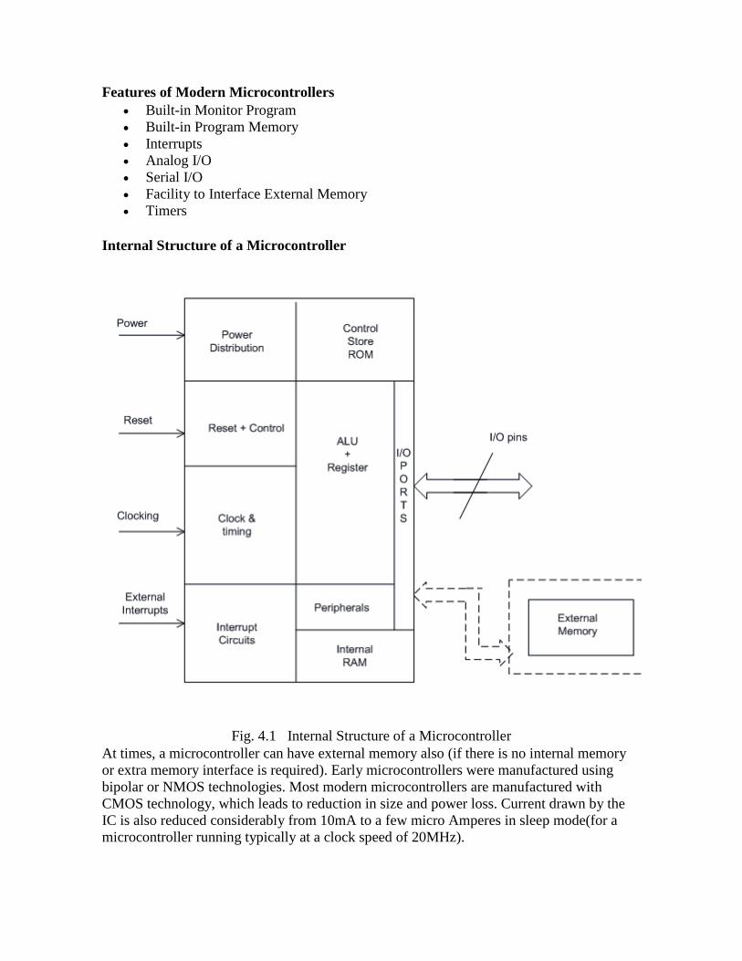
Features of Modern Microcontrollers
Built-in Monitor Program
Built-in Program Memory
Interrupts
Analog I/O
Serial I/O
Facility to Interface External Memory
Timers
Internal Structure of a Microcontroller
Fig. 4.1 Internal Structure of a Microcontroller
At times, a microcontroller can have external memory also (if there is no internal memory
or extra memory interface is required). Early microcontrollers were manufactured using
bipolar or NMOS technologies. Most modern microcontrollers are manufactured with
CMOS technology, which leads to reduction in size and power loss. Current drawn by the
IC is also reduced considerably from 10mA to a few micro Amperes in sleep mode(for a
microcontroller running typically at a clock speed of 20MHz).

Harvard Architecture (Separate Program and Data Memory interfaces)
Fig. 4.2 Harvard Arcitecture
The same instruction (as shown under Princeton Architecture) would be executed as
follows:
Cycle 1
- Complete previous instruction
- Read the "Move Data to Accumulator" instruction
Cycle 2
- Execute "Move Data to Accumulator" instruction
- Read next instruction
Hence each instruction is effectively executed in one instruction cycle, except for the ones
that modify the content of the program counter. For example, the "jump" (or call)
instructions takes 2 cycles. Thus, due to parallelism, Harvard architecture executes more
instructions in a given time compared to Princeton Architecture.
Memory organization:
In the 8051, the memory is organized logically into program memory and data memory
separately. The program memory is read-only type; the data memory is organized as read-
write memory. Again, both program and data memories can be within the chip or outside.

Basic 8051 Architecture
The 8051 is an 8-bit microcontroller i.e. the data bus within and outside the chip is eight bits
wide. The address bus of the 8051 is 16-bit wide. So it can address 64 KB of memory. The
8051 is a 40-pin chip as shown is figure below:
Fig 4.3 Pin details of 8051
8051 employs Harvard architecture. It has some peripherals such as 32 bit digital I/O,
Timers and Serial I/O. The basic architecture of 8051 is given in fig 4.4.

Fig 4.4 : Basic 8051 Architecture
Various features of 8051 microcontroller are given as follows.
8-bit CPU
16-bit Program Counter
8-bit Processor Status Word (PSW)
8-bit Stack Pointer
Internal RAM of 128bytes
Special Function Registers (SFRs) of 128 bytes
32 I/O pins arranged as four 8-bit ports (P0 - P3)
Two 16-bit timer/counters : T0 and T1
Two external and three internal vectored interrupts
One full duplex serial I/O
8051 Clock and Instruction Cycle
In 8051, one instruction cycle consists of twelve (12) clock cycles. Instruction cycle is
sometimes called as Machine cycle by some authors.
Fig 4.5 : Instruction cycle of 8051
In 8051, each instruction cycle has six states (S 1 - S 6 ). Each state has two pulses (P1 and
P2)

128 bytes of Internal RAM Structure (lower address space)
Fig 4.6: Internal RAM Structure
The lower 32 bytes are divided into 4 separate banks. Each register bank has 8 registers of
one byte each. A register bank is selected depending upon two bank select bits in the PSW
register. Next 16bytes are bit addressable. In total, 128bits (16X8) are available in
bitaddressable area. Each bit can be accessed and modified by suitable instructions. The bit
addresses are from 00H (LSB of the first byte in 20H) to 7FH (MSB of the last byte in
2FH). Remaining 80bytes of RAM are available for general purpose.
Internal Data Memory and Special Function Register (SFR) Map
Fig 4.6 : Internal Data Memory Map
The special function registers (SFRs) are mapped in the upper 128 bytes of internal data
memory address. Hence there is an address overlap between the upper 128 bytes of data
RAM and SFRs. Please note that the upper 128 bytes of data RAM are present only in the
8052 family. The lower128 bytes of RAM (00H - 7FH) can be accessed both by direct or
indirect addressing while the upper 128 bytes of RAM (80H - FFH) are accessed by indirect
addressing.The SFRs (80H - FFH) are accessed by direct addressing only. This feature
distinguishes the upper 128 bytes of memory from the SFRs, as shown in fig 4.6.
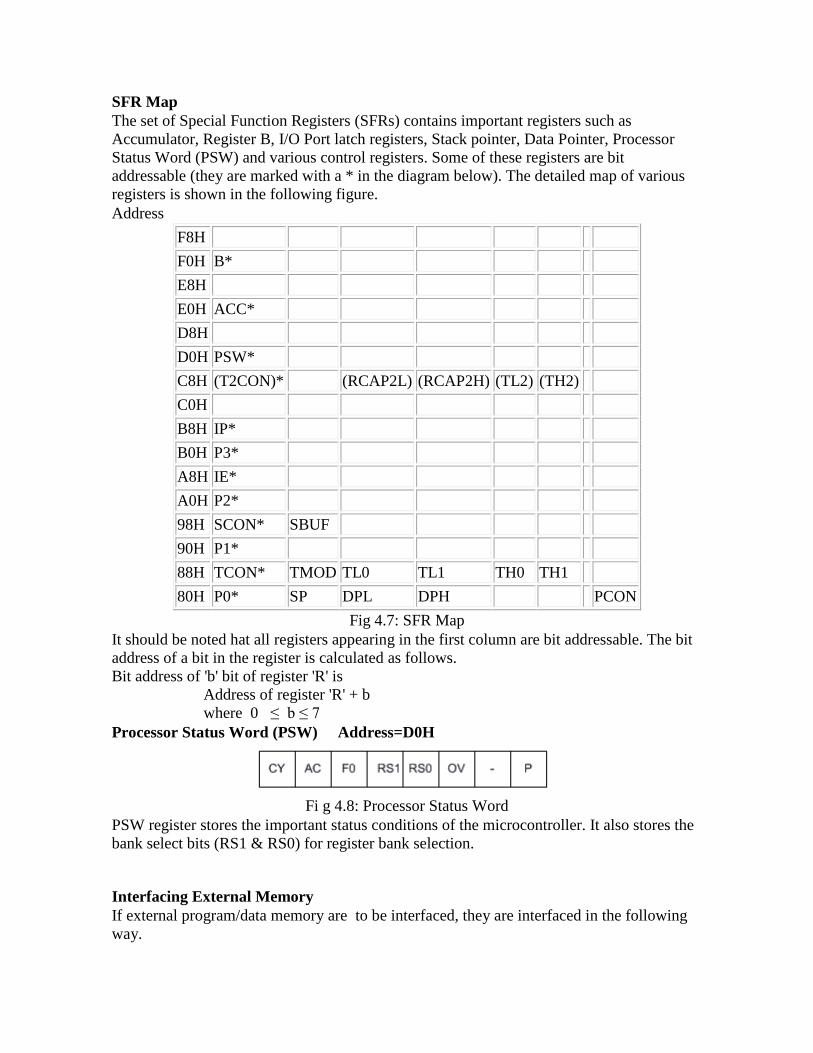
SFR Map
The set of Special Function Registers (SFRs) contains important registers such as
Accumulator, Register B, I/O Port latch registers, Stack pointer, Data Pointer, Processor
Status Word (PSW) and various control registers. Some of these registers are bit
addressable (they are marked with a * in the diagram below). The detailed map of various
registers is shown in the following figure.
Address
F8H
F0H B*
E8H
E0H ACC*
D8H
D0H PSW*
C8H (T2CON)* (RCAP2L) (RCAP2H) (TL2) (TH2)
C0H
B8H IP*
B0H P3*
A8H IE*
A0H P2*
98H SCON* SBUF
90H P1*
88H TCON* TMOD TL0 TL1 TH0 TH1
80H P0* SP DPL DPH PCON
Fig 4.7: SFR Map
It should be noted hat all registers appearing in the first column are bit addressable. The bit
address of a bit in the register is calculated as follows.
Bit address of 'b' bit of register 'R' is
Address of register 'R' + b
where 0 ≤ b ≤ 7
Processor Status Word (PSW) Address=D0H
Fi g 4.8: Processor Status Word
PSW register stores the important status conditions of the microcontroller. It also stores the
bank select bits (RS1 & RS0) for register bank selection.
Interfacing External Memory
If external program/data memory are to be interfaced, they are interfaced in the following
way.

Fig 4.9: Circuit Diagram for Interfacing of External Memory
External program memory is fetched if either of the following two conditions are
satisfied.
1. (Enable Address) is low. The microcontroller by default starts searching for
program from external program memory.
2. PC is higher than FFFH for 8051 or 1FFFH for 8052.
tells the outside world whether the external memory fetched is program memory or
data memory. is user configurable. is processor controlled.
8051 Addressing Modes
8051 has four addressing modes.
1. Immediate Addressing :
Data is immediately available in the instruction.
For example -
ADD A, #77; Adds 77 (decimal) to A and stores in A
ADD A, #4DH; Adds 4D (hexadecimal) to A and stores in A
MOV DPTR, #1000H; Moves 1000 (hexadecimal) to data pointer
2. Bank Addressing or Register Addressing :
This way of addressing accesses the bytes in the current register bank. Data is available in
the register specified in the instruction. The register bank is decided by 2 bits of Processor
Status Word (PSW).
For example-
ADD A, R0; Adds content of R0 to A and stores in A

3.. Direct Addressing :
The address of the data is available in the instruction.
For example -
MOV A, 088H; Moves content of SFR TCON (address 088H)to A
4. Register Indirect Addressing :
The address of data is available in the R0 or R1 registers as specified in the instruction.
For example -
MOV A, @R0 moves content of address pointed by R0 to A
External Data Addressing :
Pointer used for external data addressing can be either R0/R1 (256 byte access) or DPTR
(64kbyte access).
For example -
MOVX A, @R0; Moves content of 8-bit address pointed by R0 to A
MOVX A, @DPTR; Moves content of 16-bit address pointed by DPTR to A
External Code Addressing :
Sometimes we may want to store non-volatile data into the ROM e.g. look-up tables. Such
data may require reading the code memory. This may be done as follows -
MOVC A, @A+DPTR; Moves content of address pointed by A+DPTR to A
MOVC A, @A+PC; Moves content of address pointed by A+PC to A
I/O Port Configuration
Each port of 8051 has bidirectional capability. Port 0 is called 'true bidirectional port' as it
floats (tristated) when configured as input. Port-1, 2, 3 are called 'quasi bidirectional port'.
Port-0 Pin Structure
Port -0 has 8 pins (P0.0-P0.7).
The structure of a Port-0 pin is shown in fig 4.10.
Fig 4.10: Port-0 Structure

Port-0 can be configured as a normal bidirectional I/O port or it can be used for
address/data interfacing for accessing external memory. When control is '1', the port is
used for address/data interfacing. When the control is '0', the port can be used as a normal
bidirectional I/O port.
Let us assume that control is '0'. When the port is used as an input port, '1' is written to the
latch. In this situation both the output MOSFETs are 'off'. Hence the output pin floats.
This high impedance pin can be pulled up or low by an external source. When the port is
used as an output port, a '1' written to the latch again turns 'off' both the output MOSFETs
and causes the output pin to float. An external pull-up is required to output a '1'. But when
'0' is written to the latch, the pin is pulled down by the lower MOSFET. Hence the output
becomes zero.
When the control is '1', address/data bus controls the output driver MOSFETs. If the
address/data bus (internal) is '0', the upper MOSFET is 'off' and the lower MOSFET is
'on'. The output becomes '0'. If the address/data bus is '1', the upper transistor is 'on' and
the lower transistor is 'off'. Hence the output is '1'. Hence for normal address/data
interfacing (for external memory access) no pull-up resistors are required.
Port-0 latch is written to with 1's when used for external memory access.
Port-1 Pin Structure
Port-1 has 8 pins (P1.1-P1.7) .The structure of a port-1 pin is shown in fig 4.11.
Fig 4.11 Port 1 Structure
Port-1 does not have any alternate function i.e. it is dedicated solely for I/O interfacing.
When used as output port, the pin is pulled up or down through internal pull-up. To use
port-1 as input port, '1' has to be written to the latch. In this input mode when '1' is written
to the pin by the external device then it read fine. But when '0' is written to the pin by the
external device then the external source must sink current due to internal pull-up. If the
external device is not able to sink the current the pin voltage may rise, leading to a
possible wrong reading.

PORT 2 Pin Structure
Port-2 has 8-pins (P2.0-P2.7) . The structure of a port-2 pin is shown in fig 4.12.
Fig 4.12 Port 2 Structure
Port-2 is used for higher external address byte or a normal input/output port. The I/O
operation is similar to Port-1. Port-2 latch remains stable when Port-2 pin are used for
external memory access. Here again due to internal pull-up there is limited current driving
capability.
PORT 3 Pin Structure
Port-3 has 8 pin (P3.0-P3.7) . Port-3 pins have alternate functions. The structure of a port-
3 pin is shown in fig 4.13.
Fig 4.13 Port 3 Structure
Each pin of Port-3 can be individually programmed for I/O operation or for alternate
function. The alternate function can be activated only if the corresponding latch has been

written to '1'. To use the port as input port, '1' should be written to the latch. This port also
has internal pull-up and limited current driving capability.
Alternate functions of Port-3 pins are -
P3.0 RxD
P3.1 TxD
P3.2
P3.3
P3.4 T0
P3.5 T1
P3.6
P3.7
Note:
1. Port 1, 2, 3 each can drive 4 LS TTL inputs.
2. Port-0 can drive 8 LS TTL inputs in address /data mode. For digital output port, it
needs external pull-up resistors.
3. Ports-1,2and 3 pins can also be driven by open-collector or open-drain outputs.
4. Each Port 3 bit can be configured either as a normal I/O or as a special function
bit.
Reading a port (port-pins) versus reading a latch
There is a subtle difference between reading a latch and reading the output port pin.
The status of the output port pin is sometimes dependant on the connected load. For
instance if a port is configured as an output port and a '1' is written to the latch, the output
pin should also show '1'. If the output is used to drive the base of a transistor, the transistor
turns 'on'.
If the port pin is read, the value will be '0' which is corresponding to the base-emitter
voltage of the transistor.
Reading a latch: Usually the instructions that read the latch, read a value, possibly change
it, and then rewrite it to the latch. These are called "read-modify-write" instructions.
Examples of a few instructions are-
ORL P2, A; P2 <-- P2 or A
MOV P2.1, C; Move carry bit to PX.Y bit.
In this the latch value of P2 is read, is modified such that P2.1 is the same as Carry and is
then written back to P2 latch.
Reading a Pin: Examples of a few instructions that read port pin, are-
MOV A, P0 ; Move port-0 pin values to A
MOV A, P1; Move port-1 pin values to A
Accessing external memory

Access to external program memory uses the signal (Program store enable) as the
read strobe. Access to external data memory uses (alternate function of P3.7
and P3.6).
For external program memory, always 16 bit address is used. For example -
MOVC A, @ A+DPTR
MOVC A, @ A+PC
Access to external data memory can be either 8-bit address or 16-bit address -
8-bit address- MOVX A, @Rp where Rp is either R0 or R1
MOVX @Rp, A
16 bit address- MOVX A,@DPTR
MOV X @DPTR, A
The external memory access in 8051 can be shown by a schematic diagram as given in fig
4.14.
Fig 4.14 Schematic diagram of external memory access
If an 8-bit external address is used for data memory (i.e. MOVX @Rp) then the content of
Port-2 SFR remains at Port-2 pins throughout the external memory cycle. This facilitates
memory paging as the upper 8 bit address remains fixed.
During any access to external memory, the CPU writes FFH to Port-0 latch (SFR). If the
user writes to Port-0 during an external memory fetch, the incoming byte is corrupted.
External program memory is accessed under the following condition.
1. Whenever is low, or
2. Whenever PC contains a number higher than 0FFFH (for 8051) or 1FFF (for
8052).
Some typical use of code/program memory access:
External program memory can be not only used to store the code, but also for lookup table
of various functions required for a particular application. Mathematical functions such as
Sine, Square root, Exponential, etc. can be stored in the program memory (Internal or
eternal) and these functions can be accessed using MOVC instruction.

Fig 4.15 Program memory showing the storage of lookup table
Timers / Counters
8051 has two 16-bit programmable UP timers/counters. They can be configured to operate
either as timers or as event counters. The names of the two counters are T0 and T1
respectively. The timer content is available in four 8-bit special function registers, viz,
TL0,TH0,TL1 and TH1 respectively.
In the "timer" function mode, the counter is incremented in every machine cycle. Thus,
one can think of it as counting machine cycles. Hence the clock rate is 1/12 th of the
oscillator frequency.
In the "counter" function mode, the register is incremented in response to a 1 to 0
transition at its corresponding external input pin (T0 or T1). It requires 2 machine cycles
to detect a high to low transition. Hence maximum count rate is 1/24 th of oscillator
frequency.
The operation of the timers/counters is controlled by two special function registers,
TMOD and TCON respectively.
Timer Mode control (TMOD) Special Function Register:
TMOD register is not bit addressable.
TMOD
Address: 89 H
Various bits of TMOD are described as follows -
Gate: This is an OR Gate enabled bit which controls the effect of on START/STOP
of Timer. It is set to one ('1') by the program to enable the interrupt to start/stop the timer.
If TR1/0 in TCON is set and signal on pin is high then the timer starts counting
using either internal clock (timer mode) or external pulses (counter mode).
It is used for the selection of Counter/Timer mode.
Mode Select Bits:

M1 and M0 are mode select bits.
Timer/ Counter control logic:
Fig 4.16 Timer/Counter Control Logic
Timer control (TCON) Special function register:
TCON is bit addressable. The address of TCON is 88H. It is partly related to Timer and
partly to interrupt.
Fig 4.17 TCON Register
The various bits of TCON are as follows.
TF1 : Timer1 overflow flag. It is set when timer rolls from all 1s to 0s. It is cleared when
processor vectors to execute ISR located at address 001BH.
TR1 : Timer1 run control bit. Set to 1 to start the timer / counter.
TF0 : Timer0 overflow flag. (Similar to TF1)
TR0 : Timer0 run control bit.
IE1 : Interrupt1 edge flag. Set by hardware when an external interrupt edge is detected. It
is cleared when interrupt is processed.
IE0 : Interrupt0 edge flag. (Similar to IE1)
IT1 : Interrupt1 type control bit. Set/ cleared by software to specify falling edge / low
level triggered external interrupt.
IT0 : Interrupt0 type control bit. (Similar to IT1)
As mentioned earlier, Timers can operate in four different modes. They are as follows
Timer Mode-0:
In this mode, the timer is used as a 13-bit UP counter as follows.

Fig. 4.18 Operation of Timer on Mode-0
The lower 5 bits of TLX and 8 bits of THX are used for the 13 bit count.Upper 3 bits of
TLX are ignored. When the counter rolls over from all 0's to all 1's, TFX flag is set and an
interrupt is generated.
The input pulse is obtained from the previous stage. If TR1/0 bit is 1 and Gate bit is 0, the
counter continues counting up. If TR1/0 bit is 1 and Gate bit is 1, then the operation of the
counter is controlled by input. This mode is useful to measure the width of a given
pulse fed to input.
Timer Mode-1:
This mode is similar to mode-0 except for the fact that the Timer operates in 16-bit mode.
Fig 4.19 Operation of Timer in Mode 1
Timer Mode-2: (Auto-Reload Mode)
This is a 8 bit counter/timer operation. Counting is performed in TLX while THX stores a
constant value. In this mode when the timer overflows i.e. TLX becomes FFH, it is fed
with the value stored in THX. For example if we load THX with 50H then the timer in
mode 2 will count from 50H to FFH. After that 50H is again reloaded. This mode is useful
in applications like fixed time sampling.
Fig 4.20 Operation of Timer in Mode 2
Timer Mode-3:
Timer 1 in mode-3 simply holds its count. The effect is same as setting TR1=0. Timer0 in
mode-3 establishes TL0 and TH0 as two separate counters.
Fig 4.21 Operation of Timer in Mode 3

Control bits TR1 and TF1 are used by Timer-0 (higher 8 bits) (TH0) in Mode-3 while
TR0 and TF0 are available to Timer-0 lower 8 bits(TL0).
Interrupts
8051 provides 5 vectored interrupts. They are -
1. 2. TF0
3. 4. TF1
5. RI/TI
Out of these, and are external interrupts whereas Timer and Serial port interrupts
are generated internally. The external interrupts could be negative edge triggered or low
level triggered. All these interrupt, when activated, set the corresponding interrupt flags.
Except for serial interrupt, the interrupt flags are cleared when the processor branches to the
Interrupt Service Routine (ISR). The external interrupt flags are cleared on branching to
Interrupt Service Routine (ISR), provided the interrupt is negative edge triggered. For low
level triggered external interrupt as well as for serial interrupt, the corresponding flags have
to be cleared by software by the programmer.
The schematic representation of the interrupts is as follows -
Interrupt
Vector Location
Fig 4.22 8051 Interrupt Details

Each of these interrupts can be individually enabled or disabled by 'setting' or 'clearing' the
corresponding bit in the IE (Interrupt Enable Register) SFR. IE contains a global enable bit
EA which enables/disables all interrupts at once.
Interrupt Enable register (IE): Address: A8H
EX0 interrupt (External) enable bit
ET0 Timer-0 interrupt enable bit
EX1 interrupt (External) enable bit
ET1 Timer-1 interrupt enable bit
ES Serial port interrupt enable bit
ET2 Timer-2 interrupt enable bit
EA Enable/Disable all
Setting '1' Enable the corresponding interrupt
Setting '0' Disable the corresponding interrupt
Priority level structure:
Each interrupt source can be programmed to have one of the two priority levels by setting
(high priority) or clearing (low priority) a bit in the IP (Interrupt Priority) Register . A low
priority interrupt can itself be interrupted by a high priority interrupt, but not by another low
priority interrupt. If two interrupts of different priority levels are received simultaneously,
the request of higher priority level is served. If the requests of the same priority level are
received simultaneously, an internal polling sequence determines which request is to be
serviced. Thus, within each priority level, there is a second priority level determined by the
polling sequence, as follows.
Interrupt Priority register (IP)
'0' low priority
'1' high priority
Interrupt handling:
The interrupt flags are sampled at P2 of S5 of every instruction cycle (Note that every
instruction cycle has six states each consisting of P1 and P2 pulses). The samples are polled

during the next machine cycle (or instruction cycle). If one of the flags was set at S5P2 of
the preceding instruction cycle, the polling detects it and the interrupt process generates a
long call (LCALL) to the appropriate vector location of the interrupt. The LCALL is
generated provided this hardware generated LCALL is not blocked by any one of the
following conditions.
1. An interrupt of equal or higher priority level is already in progress.
2. The current polling cycle is not the final cycle in the execution of the instruction in
progress.
3. The instruction in progress is RETI or any write to IE or IP registers.
When an interrupt comes and the program is directed to the interrupt vector address, the
Program Counter (PC) value of the interrupted program is stored (pushed) on the stack. The
required Interrupt Service Routine (ISR) is executed. At the end of the ISR, the instruction
RETI returns the value of the PC from the stack and the originally interrupted program is
resumed.
Reset is a non-maskable interrupt. A reset is accomplished by holding the RST pin high for
at least two machine cycles. On resetting the program starts from 0000H and some flags are
modified as follows -
Register Value(Hex) on
Reset
PC 0000H
DPTR 0000H
A 00H
B 00H
SP 07H
PSW 00H
Ports P0-3
Latches FFH
IP XXX 00000 b
IE 0 XX 00000 b
TCON 00H
TMOD 00H
TH0 00H
TL0 00H
TH1 00H
TL1 00H
SCON 00H
SBUF XX H
PCON 0 XXXX XXX
b

The schematic diagram of the detection and processing of interrupts is given as follows.
Instruction Cycles
Fig 4.23 Interrupt Handling in 8051
It should be noted that the interrupt which is blocked due to the three conditions mentioned
before is not remembered unless the flag that generated interrupt is not still active when the
above blocking conditions are removed, i.e. ,every polling cycle is new.
Jump and Call Instructions
There are 3 types of jump instructions. They are:-
1. Relative Jump
2. Short Absolute Jump
3. Long Absolute Jump
Relative Jump
Jump that replaces the PC (program counter) content with a new address that is greater
than (the address following the jump instruction by 127 or less) or less than (the
address following the jump by 128 or less) is called a relative jump. Schematically, the
relative jump can be shown as follows: -
Fig 4.24 Relative Jump
The advantages of the relative jump are as follows:-
1. Only 1 byte of jump address needs to be specified in the 2's complement form,
ie. For jumping ahead, the range is 0 to 127 and for jumping back, the range is -

1 to -128.
2. Specifying only one byte reduces the size of the instruction and speeds up
program execution.
3. The program with relative jumps can be relocated without reassembling to
generate absolute jump addresses.
Disadvantages of the absolute jump: -
1. Short jump range (-128 to 127 from the instruction following the jump
instruction)
Instructions that use Relative Jump
SJMP <relative address>
(The remaining relative jumps are conditional jumps)
JC <relative address>
JNC <relative address>
JB bit, <relative address>
JNB bit, <relative address>
JBC bit, <relative address>
CJNE <destination byte>, <source byte>, <relative address>
DJNZ <byte>, <relative address>
JZ <relative address>
JNZ <relative address>
Short Absolute Jump
In this case only 11bits of the absolute jump address are needed. The absolute jump
address is calculated in the following manner.
In 8051, 64 kbyte of program memory space is divided into 32 pages of 2 kbyte each.
The hexadecimal addresses of the pages are given as follows:-
Page
(Hex)
Address (Hex)
00 0000 - 07FF
01 0800 - 0FFF
02 1000 - 17FF
03 1800 - 1FFF
. .
1E F000 - F7FF
1F F800 - FFFF
It can be seen that the upper 5bits of the program counter(PC) hold the page number
and the lower 11bits of the PC hold the address within that page. Thus, an absolute
address is formed by taking page numbers of the instruction (from the program
counter) following the jump and attaching the specified 11bits to it to form the 16-bit
address.
Advantage: The instruction length becomes 2 bytes.
However, difficulty is encountered when the next instruction following the jump
instruction begins from a fresh page (at X000H or at X800H). This does not give any

problem for the forward jump, but results in an error for the backward jump. In such a
case the assembler prompts the user to relocate the program suitably.
Example of short absolute jump: -
ACALL <address 11>
AJMP <address 11>
Long Absolute Jump/Call
Applications that need to access the entire program memory from 0000H to FFFFH use
long absolute jump. Since the absolute address has to be specified in the op-code, the
instruction length is 3 bytes (except for JMP @ A+DPTR). This jump is not re-
locatable.
Example: -
LCALL <address 16>
LJMP <address 16>
JMP @A+DPTR
Serial Interface
The serial port of 8051 is full duplex, i.e., it can transmit and receive simultaneously.
The register SBUF is used to hold the data. The special function register SBUF is
physically two registers. One is, write-only and is used to hold data to be transmitted
out of the 8051 via TXD. The other is, read-only and holds the received data from
external sources via RXD. Both mutually exclusive registers have the same address
099H.
Serial Port Control Register (SCON)
Register SCON controls serial data communication.
Address: 098H (Bit addressable)
Mode select bits
SM2: multi processor communication bit
REN: Receive enable bit
TB8: Transmitted bit 8 (Normally we have 0-7 bits transmitted/received)
RB8: Received bit 8
TI: Transmit interrupt flag
RI: Receive interrupt flag
Power Mode control Register
Register PCON controls processor powerdown, sleep modes and serial data bandrate.
Only one bit of PCON is used with respect to serial communication. The seventh bit
(b7)(SMOD) is used to generate the baud rate of serial communication.

Address: 87H
SMOD: Serial baud rate modify bit
GF1: General purpose user flag bit 1
GF0: General purpose user flag bit 0
PD: Power down bit
IDL: Idle mode bit
Data Transmission
Transmission of serial data begins at any time when data is written to SBUF. Pin P3.1
(Alternate function bit TXD) is used to transmit data to the serial data network. TI is
set to 1 when data has been transmitted. This signifies that SBUF is empty so that
another byte can be sent.
Data Reception
Reception of serial data begins if the receive enable bit is set to 1 for all modes. Pin
P3.0 (Alternate function bit RXD) is used to receive data from the serial data network.
Receive interrupt flag, RI, is set after the data has been received in all modes. The data
gets stored in SBUF register from where it can be read.
Serial Data Transmission Modes:
Mode-0: In this mode, the serial port works like a shift register and the data
transmission works synchronously with a clock frequency of fosc /12. Serial data is
received and transmitted through RXD. 8 bits are transmitted/ received aty a time. Pin
TXD outputs the shift clock pulses of frequency fosc /12, which is connected to the
external circuitry for synchronization. The shift frequency or baud rate is always 1/12
of the oscillator frequency.
Fig 4.25 Data transmission/reception in Mode-0
Mode-1 (standard UART mode) :
In mode-1, the serial port functions as a standard Universal Asynchronous Receiver
Transmitter (UART) mode. 10 bits are transmitted through TXD or received through
RXD. The 10 bits consist of one start bit (which is usually '0'), 8 data bits (LSB is sent
first/received first), and a stop bit (which is usually '1'). Once received, the stop bit
goes into RB8 in the special function register SCON. The baud rate is variable.
The following figure shows the way the bits are transmitted/ received.
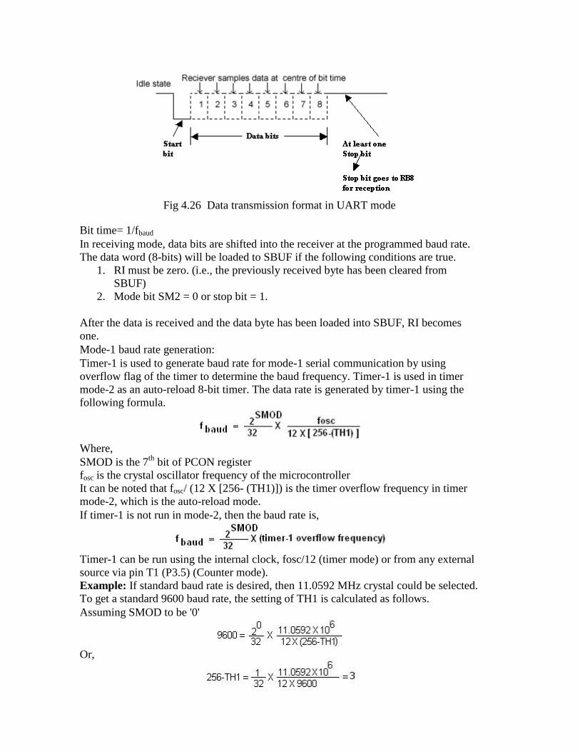
Fig 4.26 Data transmission format in UART mode
Bit time= 1/fbaud
In receiving mode, data bits are shifted into the receiver at the programmed baud rate.
The data word (8-bits) will be loaded to SBUF if the following conditions are true.
1. RI must be zero. (i.e., the previously received byte has been cleared from
SBUF)
2. Mode bit SM2 = 0 or stop bit = 1.
After the data is received and the data byte has been loaded into SBUF, RI becomes
one.
Mode-1 baud rate generation:
Timer-1 is used to generate baud rate for mode-1 serial communication by using
overflow flag of the timer to determine the baud frequency. Timer-1 is used in timer
mode-2 as an auto-reload 8-bit timer. The data rate is generated by timer-1 using the
following formula.
Where,
SMOD is the 7th
bit of PCON register
fosc is the crystal oscillator frequency of the microcontroller
It can be noted that fosc/ (12 X [256- (TH1)]) is the timer overflow frequency in timer
mode-2, which is the auto-reload mode.
If timer-1 is not run in mode-2, then the baud rate is,
Timer-1 can be run using the internal clock, fosc/12 (timer mode) or from any external
source via pin T1 (P3.5) (Counter mode).
Example: If standard baud rate is desired, then 11.0592 MHz crystal could be selected.
To get a standard 9600 baud rate, the setting of TH1 is calculated as follows.
Assuming SMOD to be '0'
Or,
Or,
In mode-1, if SM2 is set to 1, no receive interrupt (RI) is generated unless a valid stop
bit is received.
Serial Data Mode-2 - Multiprocessor Mode :
In this mode 11 bits are transmitted through TXD or received through RXD. The
various bits are as follows: a start bit (usually '0'), 8 data bits (LSB first), a
programmable 9 th
(TB8 or RB8)bit and a stop bit (usually '1').
While transmitting, the 9 th
data bit (TB8 in SCON) can be assigned the value '0' or '1'.
For example, if the information of parity is to be transmitted, the parity bit (P) in PSW
could be moved into TB8. On reception of the data, the 9 th
bit goes into RB8 in 'SCON',
while the stop bit is ignored. The baud rate is programmable to either 1/32 or 1/64 of the
oscillator frequency.
f baud = (2 SMOD
/64) fosc.
Mode-3 - Multi processor mode with variable baud rate :
In this mode 11 bits are transmitted through TXD or received through RXD. The
various bits are: a start bit (usually '0'), 8 data bits (LSB first), a programmable 9 th bit
and a stop bit (usually '1').
Mode-3 is same as mode-2, except the fact that the baud rate in mode-3 is variable (i.e.,
just as in mode-1).
f baud = (2 SMOD
/32) * ( fosc / 12 (256-TH1)) .
This baudrate holds when Timer-1 is programmed in Mode-2.
Operation in Multiprocessor mode :
8051 operates in multiprocessor mode for serial communication Mode-2 and Mode-3. In
multiprocessor mode, a Master processor can communicate with more than one slave
processors. The connection diagram of processors communicating in Multiprocessor
mode is given in fig 4.27.
The Master communicates with one slave at a time. 11 bits are transmitted by the
Master, viz, One start bit (usually '0'), 8 data bits (LSB first), TB8 and a stop bit (usually
'1'). TB8 is '1' for an address byte and '0' for a data byte.
If the Master wants to communicate with certain slave, it first sends the address of the
slave with TB8=1. This address is received by all the slaves. Slaves initially have their
SM2 bit set to '1'. All slaves check this address and the slave who is being addressed,
responds by clearing its SM2 bit to '0' so that the data bytes can be received.
It should be noted that in Mode 2&3, receive interrupt flag RI is set if REN=1, RI=0 and
the following condition is true.
1. SM2=1 and RB8=1 and a valid stop bit is received. Or
2. SM2=0 and a valid stop bit is received.

Fig 4.27 8051 in Multiprocessor Communication
After the communication between the Master and a slave has been established, the data
bytes are sent by the Master with TB8=0. Hence other slaves do not respond /get
interrupted by this data as their SM2 is pulled high (1).
Power saving modes of operation :
8051 has two power saving modes. They are -
1. Idle Mode
2. Power Down mode.
The two power saving modes are entered by setting two bits IDL and PD in the special
function register (PCON) respectively.
The structure of PCON register is as follows.
PCON: Address 87H

The schematic diagram for 'Power down' mode and 'Idle' mode is given as follows:
Fig 4.28 Schematic diagram for Power Down and Idle mode implementation
Idle Mode
Idle mode is entered by setting IDL bit to 1 (i.e., =0). The clock signal is gated off
to CPU, but not to the interrupt, timer and serial port functions. The CPU status is
preserved entirely. SP, PC, PSW, Accumulator and other registers maintain their data
during IDLE mode. The port pins hold their logical states they had at the time Idle was
initiated. ALE and are held at logic high levels.
Ways to exit Idle Mode:
1. Activation of any enabled interrupt will clear PCON.0 bit and hence the Idle
Mode is exited. The program goes to the Interrupt Service Routine (ISR). After
RETI is executed at the end of the ISR, the next instruction will start from the
one following the instruction that enabled Idle Mode.
2. A hardware reset exits the idle mode. The CPU starts from the instruction
following the instruction that invoked the 'Idle' mode.
Power Down Mode:
The Power down Mode is entered by setting the PD bit to 1. The internal clock to the
entire microcontroller is stopped (frozen). However, the program is not dead. The Power
down Mode is exited (PCON.1 is cleared to 0) by Hardware Reset only. The CPU starts
from the next instruction where the Power down Mode was invoked. Port values are not
changed/ overwritten in power down mode. Vcc can be reduced to as low as 2V in
PowerDown mode. However, Vcc has to be restored to normal value before
PowerDown mode is exited.
8051 Instructions
8051 has about 111 instructions. These can be grouped into the following categories
1. Arithmetic Instructions
2. Logical Instructions
3. Data Transfer instructions
4. Boolean Variable Instructions
5. Program Branching Instructions

The following nomenclatures for register, data, address and variables are used while write
instructions.
A: Accumulator
B: "B" register
C: Carry bit
Rn: Register R0 - R7 of the currently selected register bank
Direct: 8-bit internal direct address for data. The data could be in lower 128bytes of RAM
(00 - 7FH) or it could be in the special function register (80 - FFH).
@Ri: 8-bit external or internal RAM address available in register R0 or R1. This is used for
indirect addressing mode.
#data8: Immediate 8-bit data available in the instruction.
#data16: Immediate 16-bit data available in the instruction.
Addr11: 11-bit destination address for short absolute jump. Used by instructions AJMP &
ACALL. Jump range is 2 kbyte (one page).
Addr16: 16-bit destination address for long call or long jump.
Rel: 2's complement 8-bit offset (one - byte) used for short jump (SJMP) and all conditional
jumps.
bit: Directly addressed bit in internal RAM or SFR
Arithmetic Instructions
Mnemonics Description Bytes Instruction Cycles
ADD A, Rn A A + Rn 1 1
ADD A, direct A A + (direct) 2 1
ADD A, @Ri A A + @Ri 1 1
ADD A, #data A A + data 2 1
ADDC A, Rn A A + Rn + C 1 1
ADDC A, direct A A + (direct) + C 2 1
ADDC A, @Ri A A + @Ri + C 1 1
ADDC A, #data A A + data + C 2 1
DA A Decimal adjust accumulator 1 1
DIV AB Divide A by B
A quotient
B remainder
1 4
DEC A A A -1 1 1
DEC Rn Rn Rn - 1 1 1
DEC direct (direct) (direct) - 1 2 1

DEC @Ri @Ri @Ri - 1 1 1
INC A A A+1 1 1
INC Rn Rn Rn + 1 1 1
INC direct (direct) (direct) + 1 2 1
INC @Ri @Ri @Ri +1 1 1
INC DPTR DPTR DPTR +1 1 2
MUL AB Multiply A by B
A low byte (A*B)
B high byte (A* B)
1 4
SUBB A, Rn A A - Rn - C 1 1
SUBB A, direct A A - (direct) - C 2 1
SUBB A, @Ri A A - @Ri - C 1 1
SUBB A, #data A A - data - C 2 1
Logical Instructions
Mnemonics Description Bytes Instruction
Cycles
ANL A, Rn A A AND Rn 1 1
ANL A, direct A A AND (direct) 2 1
ANL A, @Ri A A AND @Ri 1 1
ANL A, #data A A AND data 2 1
ANL direct, A (direct) (direct) AND A 2 1
ANL direct, #data (direct) (direct) AND
data
3 2
CLR A A 00H 1 1
CPL A A A 1 1
ORL A, Rn A A OR Rn 1 1
ORL A, direct A A OR (direct) 1 1
ORL A, @Ri A A OR @Ri 2 1
ORL A, #data A A OR data 1 1
ORL direct, A (direct) (direct) OR A 2 1
ORL direct, #data (direct) (direct) OR data 3 2
RL A Rotate accumulator left 1 1
RLC A Rotate accumulator left
through carry
1 1
RR A Rotate accumulator right 1 1
RRC A Rotate accumulator right
through carry
1 1
SWAP A Swap nibbles within
Acumulator
1 1
XRL A, Rn A A EXOR Rn 1 1
XRL A, direct A A EXOR (direct) 1 1
XRL A, @Ri A A EXOR @Ri 2 1
XRL A, #data A A EXOR data 1 1

XRL direct, A (direct) (direct) EXOR A 2 1
XRL direct, #data (direct) (direct) EXOR
data
3 2
Data Transfer Instructions
Mnemonics Description Bytes Instruction
Cycles
MOV A, Rn A Rn 1 1
MOV A, direct A (direct) 2 1
MOV A, @Ri A @Ri 1 1
MOV A, #data A data 2 1
MOV Rn, A Rn A 1 1
MOV Rn,
direct
Rn (direct) 2 2
MOV Rn,
#data
Rn data 2 1
MOV direct, A (direct) A 2 1
MOV direct,
Rn
(direct) Rn 2 2
MOV direct1,
direct2
(direct1) (direct2) 3 2
MOV direct,
@Ri
(direct) @Ri 2 2
MOV direct,
#data
(direct) #data 3 2
MOV @Ri, A @Ri A 1 1
MOV @Ri,
direct
@Ri (direct) 2 2
MOV @Ri,
#data
@Ri data 2 1
MOV DPTR,
#data16
DPTR data16 3 2
MOVC A,
@A+DPTR
A Code byte pointed by A +
DPTR
1 2
MOVC A,
@A+PC
A Code byte pointed by A + PC 1 2
MOVC A,
@Ri
A Code byte pointed by Ri 8-bit
address)
1 2
MOVX A,
@DPTR
A External data pointed by
DPTR
1 2
MOVX @Ri,
A
@Ri A (External data - 8bit
address)
1 2
MOVX
@DPTR, A
@DPTR A(External data - 16bit
address)
1 2
PUSH direct (SP) (direct) 2 2

POP direct (direct) (SP) 2 2
XCH Rn Exchange A with Rn 1 1
XCH direct Exchange A with direct byte 2 1
XCH @Ri Exchange A with indirect RAM 1 1
XCHD A, @Ri Exchange least significant nibble of
A with that of indirect RAM
1 1
Boolean Variable Instructions
Mnemonics Description Bytes Instruction
Cycles
CLR C C-bit 0 1 1
CLR bit bit 0 2 1
SET C C 1 1 1
SET bit bit 1 2 1
CPL C C 1 1
CPL bit bit 2 1
ANL C, /bit C C . 2 1
ANL C, bit C C. bit 2 1
ORL C, /bit C C + 2 1
ORL C, bit C C + bit 2 1
MOV C, bit C bit 2 1
MOV bit, C bit C 2 2
Program Branching Instructions
Mnemonics Description Bytes Instruction
Cycles
ACALL addr11 PC + 2 (SP) ; addr 11 PC 2 2
AJMP addr11 Addr11 PC 2 2
CJNE A, direct,
rel
Compare with A, jump (PC + rel)
if not equal
3 2
CJNE A, #data,
rel
Compare with A, jump (PC + rel)
if not equal
3 2
CJNE Rn, #data,
rel
Compare with Rn, jump (PC +
rel) if not equal
3 2
CJNE @Ri,
#data, rel
Compare with @Ri A, jump (PC
+ rel) if not equal
3 2
DJNZ Rn, rel Decrement Rn, jump if not zero 2 2
DJNZ direct, rel Decrement (direct), jump if not
zero
3 2
JC rel Jump (PC + rel) if C bit = 1 2 2
JNC rel Jump (PC + rel) if C bit = 0 2 2
JB bit, rel Jump (PC + rel) if bit = 1 3 2
JNB bit, rel Jump (PC + rel) if bit = 0 3 2
JBC bit, rel Jump (PC + rel) if bit = 1 3 2
JMP @A+DPTR A+DPTR PC 1 2

JZ rel If A=0, jump to PC + rel 2 2
JNZ rel If A ≠ 0 , jump to PC + rel 2 2
LCALL addr16 PC + 3 (SP), addr16 PC 3 2
LJMP addr 16 Addr16 PC 3 2
NOP No operation 1 1
RET (SP) PC 1 2
RETI (SP) PC, Enable Interrupt 1 2
SJMP rel PC + 2 + rel PC 2 2
JMP @A+DPTR A+DPTR PC 1 2
JZ rel If A = 0. jump PC+ rel 2 2
JNZ rel If A ≠ 0, jump PC + rel 2 2
NOP No operation 1 1
Example programs
Character transmission using a time delay
A program shown below takes the character in 'A' register, transmits it, delays for
transmission time, and returns to the calling program. Timer-1 is used to set the baud rate,
which is 1200 baud in this program
The delay for one character transmission (in Mode 1 i.e.10 bits) is
10/2400 = 0.00833 seconds
Or, 8.33 milliseconds
Hence software delay of 10ms is used.
Timer-1 generates a baud rate close to 1200. Using a 12MHz crystal, the reload value is
Or, 230 i.e. E6H
This gives rise to an actual baud rate of 1202.
SMOD is programmed to be 0.
Assembly language Program is as follows
; Code to wait for the transmission to complete
The subroutine TRMITTIME generates a delay of about 10ms. With a clock of 12MHz, one
instruction cycle time is

The loop "MILSEC" generates a delay of about 1 x 10⁻³ sec. This gets executed 10 times
for a total delay of 10 x 10-3 sec or 10ms
Interrupt driven character transmission
In 8051, when a character is transmitted, SBUF register becomes empty and this generates a
serial port interrupt (TI). TI and RI both point to the vector location 0023H in the program
memory. An interrupt service routine can be written at 0023H to send the next character.
A program is written here to transmit a character say 'A' continuously based on interrupt.
The microcontroller uses a clock of 12MHz with a baud rate of 1202. The program is
executed following a hardware reset.
Assembly language program is as follows.
Interrupt driven data reception
When a character is received, if receive mode is enabled, RI flag is set. This leads to the
interruption of the main program and the processor goes to the interrupt vector location, i.e.

0023H for serial port. The interrupt service routine at 0023H gets executed to read the
character so that the next character can be received. The following program receives a
character on interrupt basis and outputs the character to port-1, possibly for a display.
The crystal frequency is12MHz and baud rate is set at 1202 baud.
Assembly language program is as follows

QUESTIONS:
1. Differentiate between microprocessors and microcontrollers.
2. What is a special function register?
3. Which port of 8051 is used as address/data bus?
4. What is function of RS1 and RS0 bits in the PSW of the 8051?
5. What is the address range of the bit-addressable memory of the 8051?
6. Write note on memory organization in the 8051.
7. Explain the stack operation in the 8051.
8. Where are the registers R0 – R7 located in the 8051?
9. Give one example each for one-byte, two-byte and three-byte instructions of
the 8051.
10. When the instruction DJNZ useful?
11. Write a program to multiply two 8-bit numbers in the internal RAM and
store the result in the external RAM.
12. Write a program to shift a 4-digit BCD number left by one digit. Assume that
the data is stored in 30H and 31H.
13. Write a program to reverse the bits in a byte.
14. Write a program to find the biggest number in a block of data stored in the
memory locations 70H – 7FH.
15. Write a program to generate a square wave of 10 KHz on the LSB of port 1
i.e. P1.0, using a timer.

REFERENCES:
1. 0000 to 8085 Introduction to microprocessor for scientist & engineers by Ghosh &
Sridhar, PHI.
2. Fundamentals of microprocessor and microcontroller by B. RAM, Dhanpat Rai
Publications.
3. Advanced microprocessor and peripherals (architecture, programming and
interfacing) by A.K.Roy & K.M.Bhurchandi, TMH Publication.
4. Microprocessor, theory and applications by A.V.Deshmukh, TMH Publication.