Embed Size (px)
Citation preview
Notes for ELEC220 (H.L.Kwok)
6-1
LECTURE #6: OPTICAL PROPERTIES OF SOLIDS
Basic question: How do solids interact with light?
The answers are linked to:
• Properties of light inside a solid
• Mechanisms behind light reflection, absorption and
transmission
• Type of solids and their atomic arrangement

Notes for ELEC220 (H.L.Kwok)
6-2
Light Interaction with Solids A. Properties of light • Light is energy and it has wave properties • Travels in a straight line but its direction will change across different media • Light energy E is linked to its wavelength λ through the relationship: E = hc/λ (28) where h is Planck’s constant (= 0.662 x 10⁻³³ J.s), and c (= 3 x 10⁸ m/s) is the speed of light in free-space.

Notes for ELEC220 (H.L.Kwok)
6-3
Light-solid Interactions A. Reflection • Light energy from one medium passing into another will be partially-reflected • Measured in terms of a parameter known as the reflectance
• Reflectance from air into a solid for a lossless media is given by: R = (η - 1)2/(η + 1)2 (29) where η is the index of refraction.

Notes for ELEC220 (H.L.Kwok)
6-4
Quality of the reflected light (at an air-solid interface) • Depends on the surface conditions

Notes for ELEC220 (H.L.Kwok)
6-5
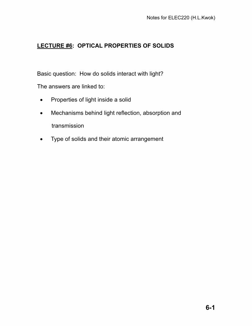
• Known as specular reflection if surface is relatively smooth, and diffuse reflection for a rough surface • Relative intensity of reflection is measured in a polar diagram - this is a plot of the intensity of reflection Iθ as a function of the angle of incidence θ: Iθ = I0 cos(θ) (30) where I0 is the light intensity when θ = 0.
Notes for ELEC220 (H.L.Kwok)
6-6
• Brightness is defined as Iθ/Aθ = I0 cos(θ)/(A0 cos(θ)) = a constant (in viewing)

Notes for ELEC220 (H.L.Kwok)
6-7
B. Transmission • Depends on the index of refraction • Light transmission from one medium into another will change direction as the velocity of light changes. • Difference in the light path is governed by Snell’s law: η1 sin(θ1) = η2 sin (θ2) (31) where η1 and η2 are the refractive indices in the two media, and θ1 and θ2 are the angle of incidence and the angle of refraction, respectively.

Notes for ELEC220 (H.L.Kwok)
6-8
Related terms • Transparency is the ability for a solid to transmit a clear image • Translucency refers to the transmission of a diffused image - often the result of scattering by small pores or particles within the solid
• Opacity implies a total loss of image transmission • Color of a solid is the result of absorption of a portion of the visible light inside the solid - impurities can be added to a transparent solid to produce specific colors

Notes for ELEC220 (H.L.Kwok)
6-9
C. Absorption • Related to a portion or all of the light energy being absorbed by the atoms or ions – energy normally ends up as heat

Notes for ELEC220 (H.L.Kwok)
6-10
• Measured in terms of an absorption coefficient which is given by: αa = ln(Φ0/Φ(x))/x (32) where x is the distance into the solid, and Φ0 is the light intensity at the surface (i.e., x = 0). Φ(x) will be the light intensity at position x.

Notes for ELEC220 (H.L.Kwok)
6-11
Light absorption in semiconductors • Results in the generation of electron and holes if the light energy exceeds the energy gap • Increase in conductivity is known as photoconductivity
• Light energy involved is often in the visible range • When light energy exceeds energy gap, surface
absorption results

Notes for ELEC220 (H.L.Kwok)
6-12
• When light energy is less than energy gap, total transmission is observed • Impurities present in semiconductors can affect the light absorption process

Notes for ELEC220 (H.L.Kwok)
6-13
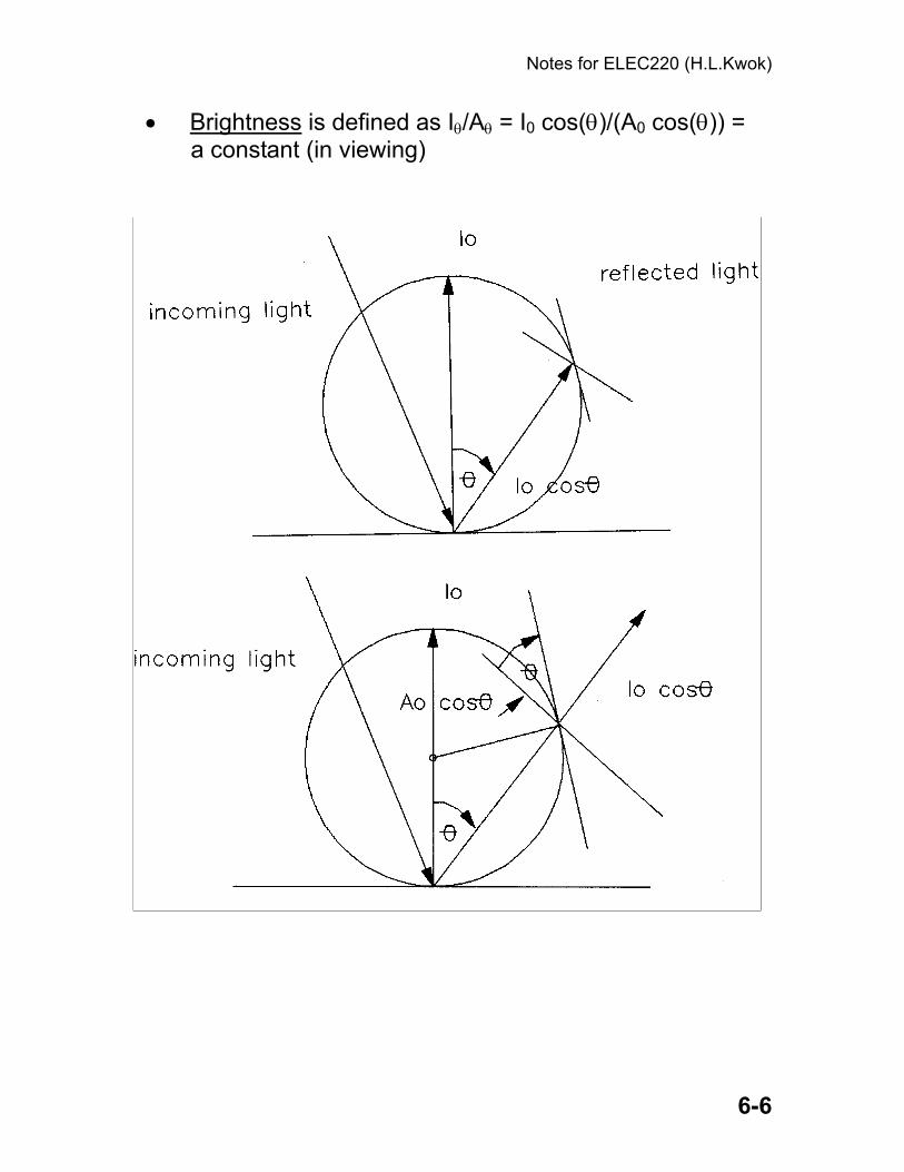
D. Emission • Occurs when excited atoms/ions return to their initial (equilibrium) states – this is known as luminescence
Notes for ELEC220 (H.L.Kwok)
6-14
• Occurs when electrons and holes recombine in a semiconductor – this is known as radiative
recombination

Notes for ELEC220 (H.L.Kwok)
6-15
• Very energetic light can cause electron emission from a metal surface - this is known as photoemission

Notes for ELEC220 (H.L.Kwok)
6-16
• All materials at a finite temperature would emit light (black-body radiation)

Notes for ELEC220 (H.L.Kwok)
6-17
Applications A. Cathode-ray tube (CRT) • A display device that relies on light generation by bombardment of a phosphor using an energetic electron beam in a process known as cathodo-luminescence
• Source of electrons is a metal electrode heated to a high temperature (electron gun) - emitted electrons are attracted to a positive electrode behind the CRT screen • Electrons hitting the phosphor on the screen recombines with the holes there and emit characteristic color light • Phosphors are usually a mixture of ZnS and CdS • Recombination has a finite time delay to generate a persistence effect • Electron beam can be deflected laterally and vertically by applying voltages to grids placed orthogonally along the beam path
Notes for ELEC220 (H.L.Kwok)
6-18
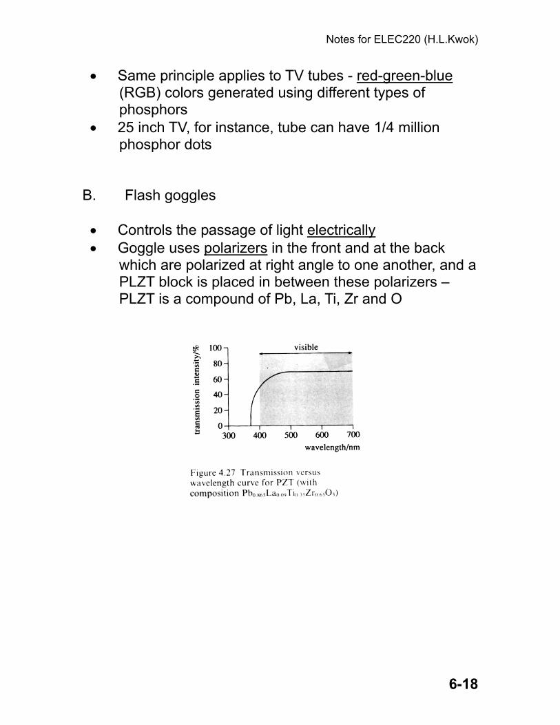
• Same principle applies to TV tubes - red-green-blue (RGB) colors generated using different types of phosphors
• 25 inch TV, for instance, tube can have 1/4 million phosphor dots
B. Flash goggles • Controls the passage of light electrically • Goggle uses polarizers in the front and at the back which are polarized at right angle to one another, and a PLZT block is placed in between these polarizers – PLZT is a compound of Pb, La, Ti, Zr and O

Notes for ELEC220 (H.L.Kwok)
6-19
• Incident light arrives at goggle (with electric field component polarized at 45 o to the right of the vertical) passes though but are reflected at the back polarizer if PLZT is inactive
Notes for ELEC220 (H.L.Kwok)
6-20
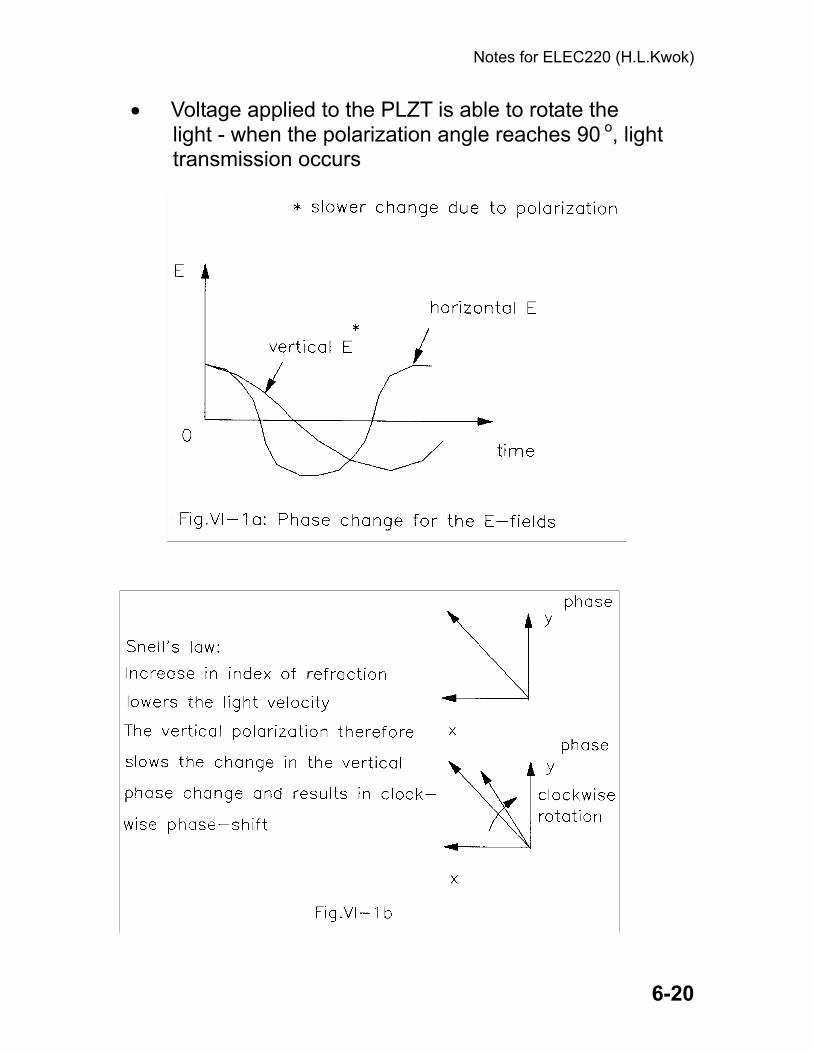
• Voltage applied to the PLZT is able to rotate the light - when the polarization angle reaches 90 o, light transmission occurs

Notes for ELEC220 (H.L.Kwok)
6-21
• Maximum light output is normally limited to about 20% • Used as an automatic light dimmer C. Liquid crystal display • Liquid crystal is a suspension of rod-like organic molecules that can have different forms of ordered structures • Different forms of ordered structure affect the optical properties of the liquid crystals by changing the index of refraction • In the natural state, liquid crystal is transparent to light • In devices light polarization is used control transmission and reflection • Power used to drive the device is capacitive and consumption is low • Device has relatively low resolution and low speed Different phases of liquid crystals a) nematic phase (NP) - molecules are randomly-placed but are parallel to one another b) cholesteric phase (CP) - molecules are parallel in every plane but are twisted from plane to plane c) smectic phase (SP) - molecules are parallel to one another and are arranged in layers

Notes for ELEC220 (H.L.Kwok)
6-22
Notes for ELEC220 (H.L.Kwok)
6-23
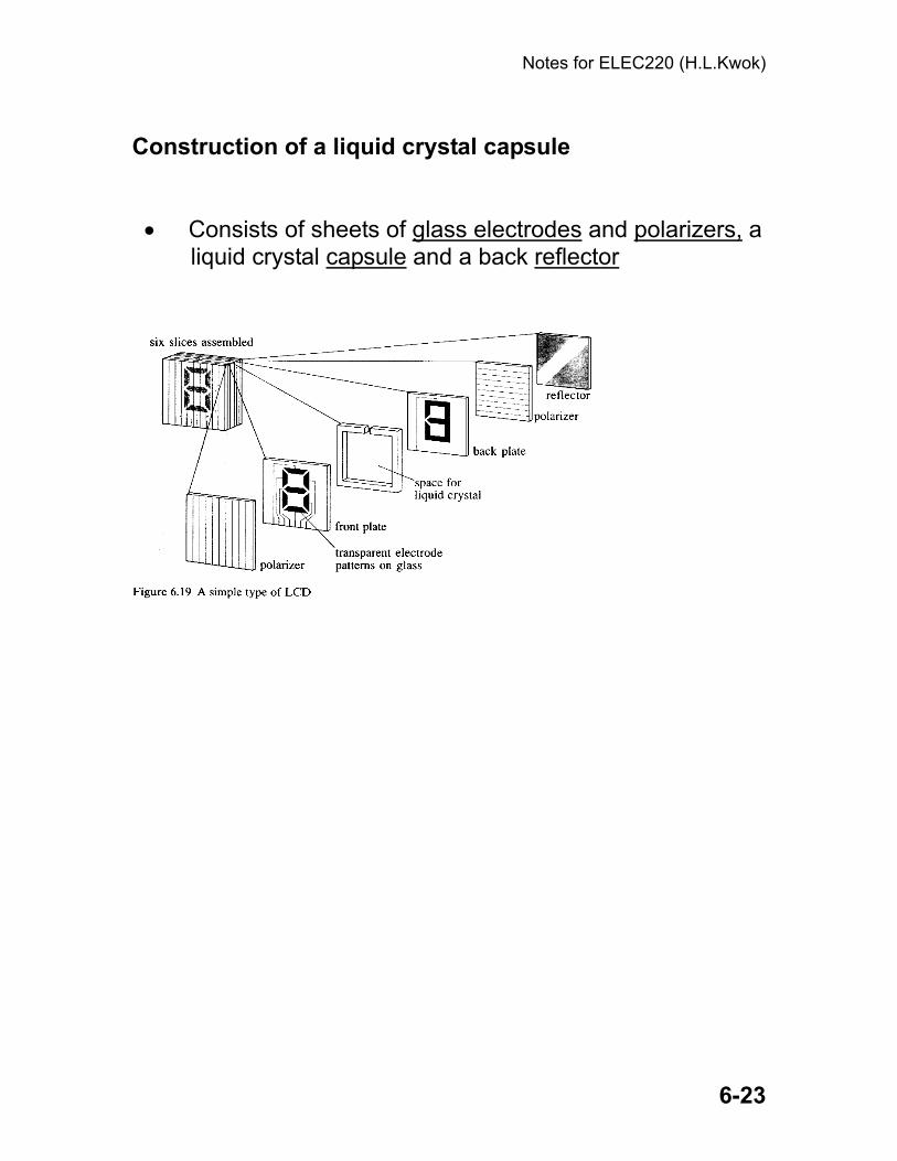
Construction of a liquid crystal capsule • Consists of sheets of glass electrodes and polarizers, a liquid crystal capsule and a back reflector

Notes for ELEC220 (H.L.Kwok)
6-24
• Glass electrodes are covered on the inside with a lined polymer pattern - the line pattern on the front and the back electrodes are 90 o off, forcing the liquid crystals (in the CP phase) inside the capsule to have the same twist
• Polarized light entering the capsule will experience a 90 o phase shift when it passes through the lower polarizer

Notes for ELEC220 (H.L.Kwok)
6-25
• Reflector reflects the incident light and the reflected
light undergoes the same phase shift resulting in a “light” pattern emerging from the capsule surface
• Electric field applied across the capsule can turn the CP phase into the NP phase and the light path is now blocked - this forms the “dark” pattern • Liquid crystal relies on “light” and “dark” patterns to form images • Most digital displays use an alpha-numeric pattern
which has 7 segments
Notes for ELEC220 (H.L.Kwok)
6-26
Example 6.1: What are the energies of light with wavelengths equal to: a) 400 nm, and b) 800 nm? What are their colors?
Solution:
The photon energy is: Ephoton = hc/λL = 6.63 x 10⁻³⁴ J.s x 3 x 10⁸ m/s/(1.6 x 10-19 C x λL ) = 1.24 eV/λL.
a) When λL = 400 nm or 0.4 µm, Ephoton = 3.1 eV (blue).
b) When λL = 800 nm or 0.8 µm, Ephoton = 1.55 eV (red).
Example 6.2: What is the number of photons per unit time emerging from a solid if the power output (of the photons) is 10 W and the (average) wavelength is 0.65 µm.
Solution:
Similar to Example 6.1, the photon energy at the wavelength of 0.65 µm is 1.9 eV. The number of photons emerging per unit time in an output of 10 W = 10 W/(1.9 eV x 1.6 x 10-19 V/eV) = 0.33 x 10²⁰ photons/s.
Example 6.3: When light passes from a medium with a high index of refraction to one with a lower value, total reflection occurs at the critical angle θcr. Compute the critical angle for light transmission from glass to air. Assume ηs(glass) = 1.46.
Solution:
Based on Snell’s law: sin(θglass) = sin(θair)/ηs(glass). Since sin(θair) = 1 and ηs(glass) = 1.46, θglass = sin-1(1/1.46) = 43.3o.
Example 6.4: Compare R*, the reflectance in silica glass (ηs = 1.46) to that in pure PbO (ηs = 2.60). Explain briefly why ornamental glassware has a small percentage of PbO present.
Solution:

Notes for ELEC220 (H.L.Kwok)
6-27
Based on the reflectance formula: R* (glass) = (1.46 - 1)2/(1.46 + 1)2 = 0.035. Similarly, R* (PbO) = (2.60 - 1)2/(2.60 + 1)2 = 0.198. PbO is therefore more reflective, which gives the ornamental value.
Example 6.5: Green light at a wavelength of 0.5 µm is allowed to shine on a piece of silicon. Estimate the distance inside the silicon when the light intensity is dropped by a factor of 100 (see Fig.E4.2).
Notes for ELEC220 (H.L.Kwok)
6-28
Solution:
From Fig.E4.2, α* is 9 x 10³ /cm when the wavelength is 0.5 µm. The distance when the light intensity is dropped by 100 is x = ln(φLo/φ)/α* = ln(100)/(9 x 103 /cm) = 5.1 x 10⁻⁴ cm.
Example 6.6: A silicon sample has a thickness of 100 µm and a conductivity of 10 S/m. If we assume that light is absorbed primarily within 2 µm from the surface and gives a photoconductivity of 1000 S/m, estimate the fractional change in the sample conductivity if the measurement is made along the semiconductor surface. Ignore any change in conductivity beyond the surface layer.
Solution:
The lateral conductivity of the sample will be the parallel combination of the conductivity of the surface layer and that of the rest of the silicon sample. The fractional change is: (σ1t1 + σ2t2)/(σ1 x (t1 + t2)) = (2 µm x 1000 S/m + 98 µm x 10 S/m)/(100 µm x 10 S/m) = 2.98.
Example 6.7: If we want to form GaInP crystal with an energy gap of 1.5 eV, what percent of GaP has to be used? For simplicity, we assume that the energy gap of GaInP depends linearly on the composition of GaP and InP and that the energy gaps of GaP and InP are 2.26 eV and 1.35 eV, respectively.
Solution: Required energy gap of GaInP is Eg = 1.5 eV = (y x 2.26 + (1 - y) x 1.35) eV, where y is the percent of InP. This leads to: y = 0.17. The composition should be 17% GaP and 83% InP.
Example 6.8: InSb is an IR detector and it has an energy gap of 0.17 eV. What is the probability that an electron in the valence band is thermally excited across the energy gap at 300K.
Solution:
Since Eg > kT (T = 300K), we can assume that the probability of carrier excitation to be: exp(- Eg/(kT)) = exp(- 0.17 eV/0.026 eV) = 1.4 x 10⁻³. This suggests that

Notes for ELEC220 (H.L.Kwok)
6-29
there will be 14 electrons excited from the valence band to the conduction band per 10,000 electrons (in the valence band).
Example 6.9: Suggest why Se thin films are unsuitable for use in electrophotography of documents with a red background.
Solution:
Although Se has an absorption threshold near 1.7 eV, the electrophotography sensitivity or photoconductivity threshold may not coincide with the absorption threshold. In fact, the photoconductivity threshold in Se is in the green (2.4 eV) and is not sensitive to red or yellow. Reflected red or yellow light from the background therefore appears as black, the same as the prints in the document.
Example 6.10: Compute the photoconductivity in a p-type photoconductor if the hole lifetime is 50 µs and the length of the photoconductor is 1000 µm. Assume the average velocity of the holes is 1 x 10⁵ m/s.
Solution:
The transit time of the photoconductor is τt = L/v = 1 x 10⁻³ m/105 m/s = 10 ns. The photoconductivity gain is τp/τt = 50 x 10-6 s/10-8 s = 5000.
Example 6.11: If a TV set has 500 x 500 pixels and the sweep frequency is 5 Mhz, how long does it take to scan the whole screen once.
Solution:
There are 500 x 500 pixels or 250,000 pixels. To achieve a sweep frequency of 5 Mhz, the maximum time delay per pixel is less than 0.1 µs (twice the sampling rate). For 1/4 million pixels, the total time delay is: 0.25 x 106 x 0.1 x 10-6 s = 0.025 s.
Example 6.12: What is the minimum number of layers of liquid crystals required to give a 90 o twist if the maximum angle between the layers is 12o.
Solution:

Notes for ELEC220 (H.L.Kwok)
6-30
The number of layers required is 90/12 =7.5 or 8 (round-off).