Embed Size (px)
Citation preview

Electric Circuits (Fall 2015) Pingqiang Zhou
Lecture 6
- Operational Amplifiers
10/20/2015
Reading: Chapter 5
Lecture 6 1

Electric Circuits (Fall 2015) Pingqiang Zhou
Outline
• Operational amplifier (op amp) model
• Ideal op amp
• Inverting op amp
• Noninverting op amp
Voltage follower
• Difference amplifier
Instrumentation amplifiers
• Differentiator/Integrator
• Application: DAC
Lecture 6 2

Electric Circuits (Fall 2015) Pingqiang Zhou
The Operational Amplifier
• The operational amplifier (“op amp”) is a
basic building block used in analog circuits.
Its behavior is modeled as dependent source
(voltage-controlled voltage source).
When combined with resistors, capacitors, and inductors,
can perform various functions:
–amplification/scaling of an input signal
–sign changing (inversion) of input signal
–addition/subtraction/multiplication/
division of input signals
– integration (over time) of an input signal
–differentiation (w.r.t. time) of an input signal
–analog filtering
–nonlinear functions like exponential, log, sqrt, etc.
Isolate input from output
Lecture 6 3
Electric Circuits (Fall 2015) Pingqiang Zhou
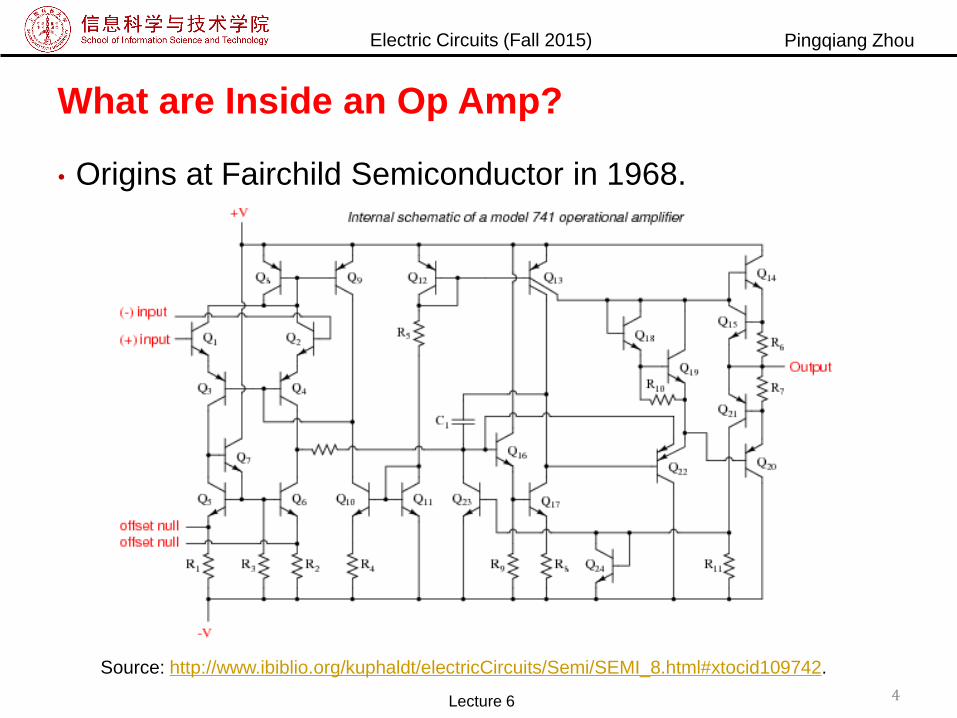
What are Inside an Op Amp?
• Origins at Fairchild Semiconductor in 1968.
4
Source: http://www.ibiblio.org/kuphaldt/electricCircuits/Semi/SEMI_8.html#xtocid109742.
Lecture 6

Electric Circuits (Fall 2015) Pingqiang Zhou
Op Amp Terminals
• Five important terminals
The inverting input
The noninverting input
The output
The positive (+) power supply
The negative (-) power supply
• The rest three terminals
2 Offset Null (Balance)
–May used in auxiliary circuit to
compensate for performance
degradation due to aging etc.
1 No Connection (NC)
– Unused, not connected to the
amplifier circuit.
Lecture 6 5

Electric Circuits (Fall 2015) Pingqiang Zhou
Powering an Op Amp
• As an active element, the op-amp
requires a power source.
• Often in circuit diagrams the power
supply terminals are obscured (ignored).
It is taken for granted that they must be
connected.
The supply current cannot be overlooked.
• Most op-amps use two voltage sources,
with a ground reference between them.
This gives a positive and negative supply
voltage.
𝑖0 = 𝑖1 + 𝑖2 + 𝑖+ + 𝑖−
Lecture 6 6

Electric Circuits (Fall 2015) Pingqiang Zhou
Output Voltage
• The voltage output of an op-amp is
proportional to the difference between
the noninverting and inverting inputs
Here, A is called the open loop gain.
Ideally A is infinite.
In real devices, it is still high: 105 to 108.
2 1( )o dv Av A v v
Lecture 6 7
𝑣2
𝑣1

Electric Circuits (Fall 2015) Pingqiang Zhou
Voltage Saturation
• Is the output voltage unlimited?
One cannot expect the output to exceed the supply voltages. When
an output should exceed the possible voltage range, the output
remains at either the maximum or minimum supply voltage. This is
called saturation.
Outputs between limiting voltages are referred to as the linear region.
𝑣0 =
−𝑉𝑐𝑐 𝐴𝑣𝑑 < −𝑉𝑐𝑐𝐴𝑣𝑑 −𝑉𝑐𝑐 ≤ 𝐴𝑣𝑑 ≤ +𝑉𝑐𝑐+𝑉𝑐𝑐 𝐴𝑣𝑑 > +𝑉𝑐𝑐
How do we know the op-amp
is operating in linear region?
Lecture 6 8
Electric Circuits (Fall 2015) Pingqiang Zhou
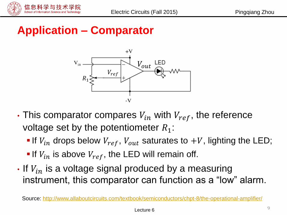
Application – Comparator
• This comparator compares 𝑉𝑖𝑛 with 𝑉𝑟𝑒𝑓, the reference
voltage set by the potentiometer 𝑅1:
If 𝑉𝑖𝑛 drops below 𝑉𝑟𝑒𝑓, 𝑉𝑜𝑢𝑡 saturates to +𝑉, lighting the LED;
If 𝑉𝑖𝑛 is above 𝑉𝑟𝑒𝑓, the LED will remain off.
• If 𝑉𝑖𝑛 is a voltage signal produced by a measuring
instrument, this comparator can function as a “low” alarm.
9
𝑅1𝑉𝑟𝑒𝑓
𝑉𝑜𝑢𝑡
Source: http://www.allaboutcircuits.com/textbook/semiconductors/chpt-8/the-operational-amplifier/
Lecture 6

Electric Circuits (Fall 2015) Pingqiang Zhou
Application – Square-Wave Converter
• The input voltage 𝑉𝑖𝑛 is an AC sine wave.
It doesn’t have to be sine wave
10
𝑉𝑟𝑒𝑓
• Useful for creating square waves of varying duty cycle
(on/off time)
Referred to as pulse-width modulation (PWM).
𝑉𝑟𝑒𝑓 𝑉𝑟𝑒𝑓
Source: http://www.allaboutcircuits.com/textbook/semiconductors/chpt-8/the-operational-amplifier/
Lecture 6

Electric Circuits (Fall 2015) Pingqiang Zhou
Feedback
• Output of the op-amp is fed back into the inverting terminal.
Feedback to the inverting terminal is called “negative feedback”.
A self-stabilizing system (also true for any dynamic system in
general), giving the op-amp the capacity to work in its linear (active)
mode.
Op-amp gain A does not have to be precisely set by the
factory in order for the circuit designer to build an amplifier
circuit with precise gain.
𝑉𝑖𝑛 ↑ ⟹ voltage differential ↑ ⟹ 𝑉𝑜𝑢𝑡 ↑⟹ voltage differential ↓ ⟹ 𝑉𝑜𝑢𝑡 ↓⟹⋯⟹ 𝑉𝑜𝑢𝑡 → 𝑉𝑖𝑛 but small difference exists
Source: http://www.allaboutcircuits.com/textbook/semiconductors/chpt-8/negative-feedback/
Lecture 6 11

Electric Circuits (Fall 2015) Pingqiang Zhou
Correct or Not?
12Lecture 6

Electric Circuits (Fall 2015) Pingqiang Zhou
Example
A 741 op amp has an open-loop voltage gain of 2 × 10⁵, input
resistance of 2𝑀Ω, and output resistance of 50Ω. Find the
closed-loop gain 𝑣𝑜/𝑣𝑠. Determine current 𝑖 when 𝑣𝑠 = 2𝑉.
13
𝑣𝑠 − 𝑣110𝑘Ω
=𝑣1 − 𝑣𝑜20𝑘Ω
+𝑣12𝑀Ω
𝑣1 − 𝑣𝑜20𝑘Ω
=𝑣𝑜 − 𝐴𝑣𝑑50Ω
𝑣𝑜𝑣𝑠
= −1.9999699
𝑣1 = 20.066667𝜇𝑉
20.066667𝜇𝑉−3.9999398𝑉
Lecture 6

Electric Circuits (Fall 2015) Pingqiang Zhou
Ideal Op Amp
• Attributes of ideal op-amp:
infinite open-loop gain, 𝐴 ⋍ ∞– Implies that 𝑣2 = 𝑣1.
infinite resistance of the two
inputs, 𝑅𝑖 ⋍ ∞
–This means it will not affect any
node it is attached to
– Implies that 𝑖1 = 𝑖2 = 0.
zero output impedance, 𝑅𝑜 ⋍ 0–From Thevenin’s theorem one can
see that this means it is load
independent.
20.066667𝜇𝑉 −3.9999398𝑉
Lecture 6 14

Electric Circuits (Fall 2015) Pingqiang Zhou
Comments on Negative Feedback
• The basic principle of negative feedback is that the output
tends to drive in a direction that creates a condition of
equilibrium (balance).
With negative feedback, the circuit tends to prevent itself from
driving the output to a full saturation.
–Whether the output is directly fed back to the inverting (-) input or
coupled through a set of components, the effect is the same: the
extremely high differential voltage gain of the op-amp will be “tamed”
and the circuit will respond according to the dictates of the feedback
“loop” connecting output to inverting input.
15
Negative feedback
Source: http://www.allaboutcircuits.com/textbook/semiconductors/chpt-8/negative-feedback/
Lecture 6

Electric Circuits (Fall 2015) Pingqiang Zhou
Positive Feedback
• The inverting terminal is free to receive an
external voltage.
• Let’s see what happens if we ground the
inverting input:
𝑉𝑜𝑢𝑡 will be dictated by the magnitude and
polarity of 𝑉𝑝𝑙𝑢𝑠
–Small +𝑉𝑝𝑙𝑢𝑠 ⟹ large +𝑉𝑜𝑢𝑡 ⟹ full positive
output saturation because of feedback.
–Small -𝑉𝑝𝑙𝑢𝑠 ⟹ large -𝑉𝑜𝑢𝑡 ⟹ full negative
output saturation because of feedback.
16
Sources:
• http://www.allaboutcircuits.com/textbook/semiconductors/chpt-8/positive-feedback/
• http://ocw.mit.edu/courses/electrical-engineering-and-computer-science/6-002-circuits-and-
electronics-spring-2007/video-lectures/lecture-21/
Positive feedback
𝑉𝑝𝑙𝑢𝑠
▪ Bistable output: either saturated positive or saturated negative
▪ Known as hysteresis.
Lecture 6

Electric Circuits (Fall 2015) Pingqiang Zhou
Application - Hysteresis
17
Glitch
Source: http://www.allaboutcircuits.com/textbook/semiconductors/chpt-8/positive-feedback/
• When 𝑉𝑜𝑢𝑡 is saturated positive,
𝑉𝑟𝑒𝑓 will be more positive than before.
• When 𝑉𝑜𝑢𝑡 is saturated negative, 𝑉𝑟𝑒𝑓will be more negative than before.
𝑉𝑟𝑒𝑓
𝑉𝑟𝑒𝑓
Lecture 6

Electric Circuits (Fall 2015) Pingqiang Zhou
Application - Oscillator
• Oscillator is a device that produces an alternating, or at
least pulsing, output voltage.
Known as astable device, no stable output state.
18
• When 𝑉𝑜𝑢𝑡 is saturated positive, 𝑉𝑟𝑒𝑓 is positive, capacitor 𝐶 charges up.
• When 𝑉𝑟𝑎𝑚𝑝 exceeds 𝑉𝑟𝑒𝑓 by the tiniest margin, 𝑉𝑜𝑢𝑡 becomes saturated
negative, and 𝐶 will charge in the opposite direction (polarity).
• Oscillation occurs because
positive feedback is instantaneous,
negative feedback is delayed by means of an RC time constant.
Source: http://www.allaboutcircuits.com/textbook/semiconductors/chpt-8/positive-feedback/Lecture 6

Electric Circuits (Fall 2015) Pingqiang Zhou
Ideal Op Amp
• Attributes of ideal op-amp:
infinite open-loop gain, 𝐴 ⋍ ∞– Implies that 𝑣2 = 𝑣1.
infinite resistance of the two
inputs, 𝑅𝑖 ⋍ ∞
–This means it will not affect any
node it is attached to
– Implies that 𝑖1 = 𝑖2 = 0.
zero output impedance, 𝑅𝑜 ⋍ 0–From Thevenin’s theorem one can
see that this means it is load
independent
Lecture 6 19

Electric Circuits (Fall 2015) Pingqiang Zhou
Ideal Op-Amp Analysis Technique
Assumption 1: The potential between the op-amp input terminals, v(+) –
v(-), equals zero.
R2R1
+
V0VIN
EXAMPLE
Assumption 2: The currents flowing into the op-amp’s two input
terminals both equal zero.
No Potential DifferenceNo Currents
Lecture 6 20

Electric Circuits (Fall 2015) Pingqiang Zhou
21Lecture 6
Ideal Op-Amp Analysis: Inverting Amplifier
R2
I2
VOUT-VR
R1
RLVIN
021
R
VV
R
VV OUTRINR
RinROUT VVR
RVV
1
2
Only two
currents
for KCL
When 𝑉𝑅 = 0, 𝑉𝑂𝑈𝑇 = −𝑅2
𝑅1𝑉𝐼𝑁
From this one can see that:• Closed-loop gain = ratio of feedback resistor 𝑅2 and 𝑅1.
• The polarity of output 𝑉𝑂𝑈𝑇 is the reverse of the input,
thus the name “inverting” amplifier.
• 𝑉𝑂𝑈𝑇 independent of 𝑅𝐿 - ideal voltage source
VR

Electric Circuits (Fall 2015) Pingqiang Zhou
22Lecture 6
Practice
• Determine 𝑣𝑜 in the circuit shown below

Electric Circuits (Fall 2015) Pingqiang Zhou
Equivalent Circuit of Inverting Amplifier
• The equivalent circuit
has a finite input resistance
a good candidate for making a
current-to-voltage converter
𝑣𝑜 = −𝑅𝑓
𝑅1𝑣𝑖
Lecture 6 23

Electric Circuits (Fall 2015) Pingqiang Zhou
Ideal Op-Analysis: Non-Inverting Amplifier
Assumption 1: The potential between the op-amp input terminals, v(+) –
v(-), equals zero.
R2R1
+
VoutVIN
Assumption 2: The currents flowing into the op-amp’s two input
terminals both equal zero.
021
R
vv
R
v outinin
inout vR
Rv
1
21
KCL with currents in only two branches
Non-inverting AmplifierVIN appears here
Lecture 6 24

Electric Circuits (Fall 2015) Pingqiang Zhou
25Lecture 6
Non-Inverting Amplifier
_
+
vin+-
R2
R1
RL
v2
vo
2
• Closed-loop gain
𝐴 =𝑣𝑜
𝑣𝑖𝑛= 1 +
𝑅2
𝑅1
• Input impedance = ∞
_
+
vin+- RL
v2
v0
• Voltage follower
𝑅2 = 0, 𝑅1 = ∞
𝑣𝑜 = 𝑣𝑖𝑛 (𝐴 = 1)
separating two circuits while
allowing a signal to pass
through.

Electric Circuits (Fall 2015) Pingqiang Zhou
Practice
• Find 𝑣𝑜
26Lecture 6

Electric Circuits (Fall 2015) Pingqiang Zhou
Summing Amplifier
• Aside from amplification, the op-amp can be made to do
addition very readily.
• If one takes the inverting amplifier and combines several
inputs each via their own resistor:
The current from each input will be proportional to the applied
voltage and the input resistance
1 2 3
1 2 3
1 2 3
a a av v v v v vi i i
R R R
𝑖 = 𝑖1 + 𝑖2 + 𝑖3 =𝑣𝑎 − 𝑣𝑜𝑅𝑓
, 𝑣𝑎 = 0
𝑣𝑜 = −𝑅𝑓
𝑅1𝑣1 +
𝑅𝑓
𝑅2𝑣2 +
𝑅𝑓
𝑅3𝑣3
Lecture 6 27

Electric Circuits (Fall 2015) Pingqiang Zhou
Practice
• Find 𝑣𝑜 and 𝑖𝑜 in the circuit shown below
28Lecture 6

Electric Circuits (Fall 2015) Pingqiang Zhou
Difference (or Differential) Amplifier
• Subtraction should come
naturally to the op-amp
since its output proportional
to the difference between
the two inputs.
• An op-amp with no feedback
is already a differential
amplifier, amplifying the
voltage difference between
the two inputs. However, its
gain cannot be controlled,
and it is generally too high to
be of any practical use.
2 21
1 1
1o a
R Rv v v
R R
42
3 4
b
Rv v
R R
2 1 2 2
2 1
1 3 4 1
1
1o
R R R Rv v v
R R R R
Lecture 6 29

Electric Circuits (Fall 2015) Pingqiang Zhou
Common Mode Rejection
• It is important that a difference amplifier reject any signal
that is common to the two inputs.
Which implies that when 𝑣1 = 𝑣2, 𝑣𝑜 = 0.
• For the given circuit, this is true if𝑅1
𝑅2=
𝑅3
𝑅4, then
2 1 2 2
2 1
1 3 4 1
1
1o
R R R Rv v v
R R R R
𝑣𝑜 =𝑅2𝑅1
𝑣2 − 𝑣1
Lecture 6 30

Electric Circuits (Fall 2015) Pingqiang Zhou
Example
• Design an op amp circuit with inputs 𝑣1 and 𝑣2 such that
𝑣𝑜 = −5𝑣1 + 3𝑣2.
31
2 1 2 2
2 1
1 3 4 1
1
1o
R R R Rv v v
R R R R
⟹ 𝑅2
𝑅1= 5,
𝑅2 1 + 𝑅1/𝑅2𝑅1 1 + 𝑅3/𝑅4
= 3
⟹ 𝑅3𝑅4
= 1
Lecture 6

Electric Circuits (Fall 2015) Pingqiang Zhou
Example – An Instrumental Amplifier
• Show that 𝑣0 =𝑅2
𝑅11 + 2
𝑅3
𝑅4𝑣2 − 𝑣1 .
32
𝑣0 =𝑅2𝑅1
𝑣02 − 𝑣01
𝑣01 − 𝑣02 = 𝑖 2𝑅3 + 𝑅4
𝑖 =𝑣1 − 𝑣2𝑅4
Lecture 6

Electric Circuits (Fall 2015) Pingqiang Zhou
Practice
• Obtain 𝑖𝑜 in the following instrumentation amplifier circuit
33Lecture 6

Electric Circuits (Fall 2015) Pingqiang Zhou
Limitation with the Difference Amplifier
• One significant drawback:
The input impedance is low.
Each input voltage source has to
drive current through a
resistance, which constitutes far
less impedance than the bare
input of an op-amp alone.
• By placing a noninverting
amplifier stage before the
difference amplifier this can
be resolved.
Source: http://www.allaboutcircuits.com/textbook/semiconductors/chpt-8/building-a-differential-amplifier/
Lecture 6 34

Electric Circuits (Fall 2015) Pingqiang Zhou
Instrumentation Amplifier
• It is beneficial to be able to adjust the gain of the amplifier
circuit without having to change more than one resistor
value
• Instrumentation amplifier has this capability
a buffered differential amplifier stage with three new resistors
𝑉𝑜𝑢𝑡 = 1 +2𝑅
𝑅𝑔𝑎𝑖𝑛𝑉2 − 𝑉1
Overall gain 𝐴𝑣 = 1 +2𝑅
𝑅𝑔𝑎𝑖𝑛
Source: http://www.allaboutcircuits.com/textbook/semiconductors/chpt-8/the-instrumentation-amplifier/
Lecture 6 35

Electric Circuits (Fall 2015) Pingqiang Zhou
Instrumentation Amplifier
• Instrumentation amplifiers are so useful, they are often
packaged as a single chip with the only external
component being the gain resistor
• They are very effective at extracting a weak differential
signal out of a large common mode signal
In circuits exposed to external electrical noise, this is
important in order to maintain a high signal-to-noise ratio.
Lecture 6 36

Electric Circuits (Fall 2015) Pingqiang Zhou
Differentiator
• The differentiator (not to be confused with differential)
produces a voltage output proportional to the input
voltage’s rate of change.
• Want
• By introducing electrical reactance into the feedback loops
of op-amp amplifier circuits, we can cause the output to
respond to changes in the input voltage over time.
𝑣𝑜 = 𝐾 ∙𝑑𝑣𝑖𝑑𝑡
Source: http://www.allaboutcircuits.com/textbook/semiconductors/chpt-8/differentiator-integrator-circuits/
Lecture 6 37

Electric Circuits (Fall 2015) Pingqiang Zhou
Differentiator
• We can build an op-amp circuit which measures change
in voltage by measuring current through a capacitor, and
outputs a voltage proportional to that current:
38
i
The RHS of the capacitor is held to
a voltage of 0 volts, due to the
“virtual ground”effect. Therefore,
current“through”the capacitor is
solely due to change in the input
voltage.
Capacitor current moves through the
feedback resistor, producing a drop
across it, which is the same as the
output voltage.
Source: http://www.allaboutcircuits.com/textbook/semiconductors/chpt-8/differentiator-integrator-circuits/
Lecture 6

Electric Circuits (Fall 2015) Pingqiang Zhou
Integrator
• The integrator produces a voltage
output proportional to the product
(multiplication) of the input voltage
and time.
• Want
o inv K v dt
R+
-C V0
+
-
vin
𝑣0 =1
𝑅𝐶
−∞
𝑡
𝑣𝑖𝑛 𝑑𝑡 =1
𝐶
−∞
𝑡𝑣𝑖𝑛𝑅𝑑𝑡
Electric Circuits (Fall 2015) Pingqiang Zhou
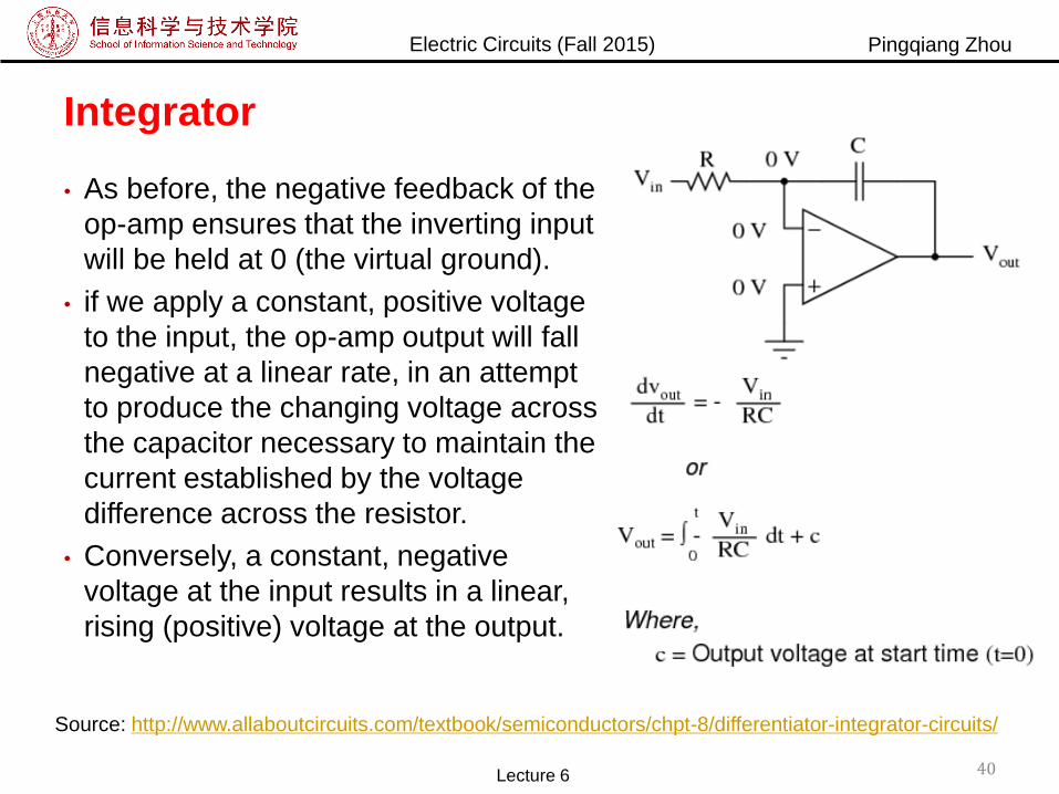
Integrator
• As before, the negative feedback of the
op-amp ensures that the inverting input
will be held at 0 (the virtual ground).
• if we apply a constant, positive voltage
to the input, the op-amp output will fall
negative at a linear rate, in an attempt
to produce the changing voltage across
the capacitor necessary to maintain the
current established by the voltage
difference across the resistor.
• Conversely, a constant, negative
voltage at the input results in a linear,
rising (positive) voltage at the output.
40
Source: http://www.allaboutcircuits.com/textbook/semiconductors/chpt-8/differentiator-integrator-circuits/
Lecture 6

Electric Circuits (Fall 2015) Pingqiang Zhou
Cascaded Op Amps
• It is common to use multiple op-amp stages chained
together.
• This head to tail configuration is called “cascading”.
• Each amplifier is then called a “stage”.
• The gain of a series of amplifiers is the product of the
individual gains:
𝐴 = 𝐴1 ∙ 𝐴2 ∙ 𝐴3
Lecture 6 41

Electric Circuits (Fall 2015) Pingqiang Zhou
Application - Digital to Analog Converter
• The function of a digital to analog converter (DAC) is to
take a series of binary values that represent a number
and convert it to an analog voltage
In a digital signal, the input voltage will be either zero which
represents ‘0’ or a non-zero voltage which represents ‘1’
• The summing amplifier can be used to create simple DAC
Recall that each input has its own multiplier resistor
𝑣𝑜 = −𝑅𝑓
𝑅1𝑣1 +
𝑅𝑓
𝑅2𝑣2 +
𝑅𝑓
𝑅3𝑣3
Lecture 6 42

Electric Circuits (Fall 2015) Pingqiang Zhou
Digital to Analog Converter
• By selecting the input resistors 𝑅𝑖s
such that each input will have a
weighting according to the
magnitude of their place value
Each lesser bit will have half the
weight of the next higher bit
• The feedback resistor 𝑅𝑓 provides
an overall scaling, allowing the
output to be adjusted according to
the desired range
−𝑉𝑜 =𝑅𝑓
𝑅1𝑉1 +
𝑅𝑓
𝑅2𝑉2 +
𝑅𝑓
𝑅3𝑉3 +
𝑅𝑓
𝑅4𝑉4
Lecture 6 43

Electric Circuits (Fall 2015) Pingqiang Zhou
A DAC can be used to convert the digital representation
of an audio signal into an analog voltage that is then
used to drive speakers -- so that you can hear it!
0 0 1 0 10 0 1 10 1 0 0
1.52
0 1 0 10 1 1 00 1 1 11 0 0 0
2.53
3.54
1 0 0 11 0 1 01 0 1 11 1 0 01 1 0 11 1 1 01 1 1 1
4.55
5.56
6.57
7.5
Binarynumber
Analogoutput(−𝑉𝑜)
0 0 0 00 0 0 1
0.5
MSB LSB
S1 closed if LSB =1
S2 " if next bit = 1
S3 " if " " = 1
S4 " if MSB = 1
4-Bit D/A
8V
+ V0
5K
80K
40K
20K
10K
S1
+-
S3
S2
S4
+
DAC Example
“Weighted-adder D/A converter”
(Transistors are used
as electronic switches)

Electric Circuits (Fall 2015) Pingqiang Zhou
Digital Input
0
1
2
3
4
5
6
7
8
0 2 4 6 8 10 12 14 16
An
alo
g O
utp
ut
(V)
111110000100
0000 0001
Characteristic of 4-Bit DAC

Electric Circuits (Fall 2015) Pingqiang Zhou
Summary
Lecture 6 46

Electric Circuits (Fall 2015) Pingqiang Zhou
To Read Further…
• Nonlinear Circuits
Online notes “Introduction to nonlinear circuit analysis” from
Berkeley.
Ch. 4 in reference: Anant Agarwal and Jeffrey Lang, Foundations of
Analog and Digital Electronic Circuits, Morgan Kaufmann, 2005.
• More about Op Amps
Online textbook http://www.allaboutcircuits.com/textbook/semiconductors/chpt-8/
Lecture 6 47