Embed Size (px)
Citation preview

Lecture 4
OUTLINE• Semiconductor Fundamentals (cont’d)
– Properties of carriers in semiconductors– Carrier drift
• Scattering mechanisms• Drift current
– Conductivity and resistivity
Reading: Pierret 3.1; Hu 1.5, 2.1-2.2

Mobile Charge Carriers in Semiconductors
• Three primary types of carrier action occur inside a semiconductor:
– Drift: charged particle motion under the influence of an electric field.
– Diffusion: particle motion due to concentration gradient or temperature gradient.
– Recombination-generation (R-G)
EE130/230M Spring 2013 Lecture 4, Slide 2

Electrons as Moving Particles
F = (-q)E = moa F = (-q)E = mn*a
where mn* is the conductivity effective mass
In vacuum In semiconductor
EE130/230M Spring 2013 Lecture 4, Slide 3

Conductivity Effective Mass, m*Under the influence of an electric field (E-field), an electron or a hole is accelerated:
electrons
holes
acceleration qE–mn---------=
*nm
qa
*pm
qa
EE130/230M Spring 2013 Lecture 4, Slide 4
Si Ge GaAsmn*/mo 0.26 0.12 0.068
mp*/mo 0.39 0.30 0.50
mo = 9.110-31 kg
Electron and hole conductivity effective masses

Carrier Scattering• Mobile electrons and atoms in the Si lattice are always in
random thermal motion.– Electrons make frequent collisions with the vibrating atoms
“lattice scattering” or “phonon scattering” – increases with increasing T
• Other scattering mechanisms:– deflection by ionized impurity atoms– deflection due to Coulombic force between carriers
“carrier-carrier scattering” – only significant at high carrier concentrations
• The net current in any direction is zero, if no E-field is applied.
123
45
electron
EE130/230M Spring 2013 Lecture 4, Slide 5

Thermal Velocity, vth
Average electron kinetic energy 2*
2
1
2
3thnvmkT
cm/s103.2m/s103.2
kg101.926.0
J/eV)106.1(eV026.033
75
31
19
*
nth m
kTv
EE130/230M Spring 2013 Lecture 4, Slide 6

Carrier Drift• When an electric field (e.g. due to an externally applied voltage)
exists within a semiconductor, mobile charge-carriers will be accelerated by the electrostatic force:
12
3
45
electron
EElectrons drift in the direction opposite to the E-field net current
Because of scattering, electrons in a semiconductor do not undergo constant acceleration. However, they can be viewed as quasi-classical particles moving at a constant average drift velocity vdn
EE130/230M Spring 2013 Lecture 4, Slide 7
Carrier Drift (Band Model)
Ec
Ev
EE130/230M Spring 2013 Lecture 4, Slide 8

Electron Momentum• With every collision, the electron loses momentum
• Between collisions, the electron gains momentum–qEmn
mn ≡ average time between electron scattering events
dnnvm*
EE130/230M Spring 2013 Lecture 4, Slide 9
Conservation of momentum |mn*vdn | = | qEmn|

Carrier Mobility, |vdn| = qEmn / mn* ≡ nE
n [qmn / mn*] is the electron mobility
p [qmp / mp*] is the hole mobility
Similarly, for holes: |vdp|= qEmp / mp* pE
EE130/230M Spring 2013 Lecture 4, Slide 10
Si Ge GaAs InAsn (cm2/Vs) 1400 3900 8500 30,000
p (cm2/Vs) 470 1900 400 500
Electron and hole mobilities for intrinsic semiconductors @ 300K
For electrons:

Example: Drift Velocity Calculationa) Find the hole drift velocity in an intrinsic Si sample for E = 103 V/cm.
b) What is the average hole scattering time?
vdp = pE
q
m
m
q ppmp
p
mpp
*
*
EE130/230M Spring 2013 Lecture 4, Slide 11
Solution:
a)
b)

Mean Free Path• Average distance traveled between collisions
mpthvl
EE130/230M Spring 2013 Lecture 4, Slide 12

Mechanisms of Carrier ScatteringDominant scattering mechanisms:
1. Phonon scattering (lattice scattering)2. Impurity (dopant) ion scattering
2/32/1
1
velocityermalcarrier thdensityphonon
1
TTTphononphonon
Phonon scattering limited mobility decreases with increasing T:
= q / m Tvth
EE130/230M Spring 2013 Lecture 4, Slide 13

Impurity Ion Scattering
DADA
thimpurity NN
T
NN
v
2/33
There is less change in the electron’s direction if the electron travels by the ion at a higher speed.
EE130/230M Spring 2013 Lecture 4, Slide 14
Ion scattering limited mobility increases with increasing T:

Matthiessen's Rule
Probability that a carrier will be scattered by any mechanism
within a time period dt is
impurityphononimpurityphonon 111
111
i i
dt
i
dt
EE130/230M Spring 2013 Lecture 4, Slide 15
• The probability that a carrier will be scattered by mechanism i
within a time period dt is
i ≡ mean time between scattering events due to mechanism i
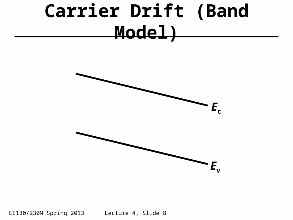
Mobility Dependence on DopingCarrier mobilities in Si at 300K
EE130/230M Spring 2013 Lecture 4, Slide 16

Mobility Dependence on Temperature
impurityphonon 111
EE130/230M Spring 2013 Lecture 4, Slide 17

Hole Drift Current Density, Jp,drift
vdp t A = volume from which all holes cross plane in time t
p vdp t A = number of holes crossing plane in time t
q p vdp t A = hole charge crossing plane in time t
q p vdp A = hole charge crossing plane per unit time = hole current
Hole drift current per unit area Jp,drift = q p vdpEE130/230M Spring 2013 Lecture 4, Slide 18

Conductivity and Resistivity
EE130/230M Spring 2013 Lecture 4, Slide 19
EEqnqpJ npdrift )(
)( ,, EqnJEqpJ ndriftnpdriftp
EqnEqpJJJ npdriftndriftpdrift ,,
• In a semiconductor, both electrons and holes conduct current:
np qnqp • The conductivity of a semiconductor is– Unit: mho/cm
1
• The resistivity of a semiconductor is– Unit: ohm-cm

Resistivity Dependence on Doping
n-type
p-type
EE130/230M Spring 2013 Lecture 4, Slide 20
For n-type material:
nqn 1
For p-type material:
pqp 1
Note: This plot (for Si) does not apply to compensated material (doped with both acceptors and donors).

Electrical Resistance
where is the resistivity
Resistance Wt
L
I
VR [Unit: ohms]
V+ _
L
tW
I
uniformly doped semiconductor
EE130/230M Spring 2013 Lecture 4, Slide 21

Example: Resistance CalculationWhat is the resistivity of a Si sample doped with 1016/cm3 Boron?
Answer:
cm 4.1)450)(10)(106.1(
11
11619
ppn qpqpqn
EE130/230M Spring 2013 Lecture 4, Slide 22
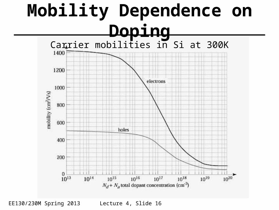
Example: Dopant Compensation
cm 12.0)600)(109)(106.1(
11
11619
npn qnqpqn
Consider the same Si sample doped with 1016/cm3 Boron, and additionally doped with 1017/cm3 Arsenic. What is its resistivity?Answer:
EE130/230M Spring 2013 Lecture 4, Slide 23

Example: T Dependence of
Consider a Si sample doped with 1017cm-3 As. How will its resistivity change when the temperature is increased from T=300K to T=400K?
93.1400
770
EE130/230M Spring 2013 Lecture 4, Slide 24
Answer: The temperature dependent factor in (and therefore ) is n.
From the mobility vs. temperature curve for 1017 cm-3, we find that n decreases from 770 at 300K to 400 at 400K.
Thus, increases by

Summary• Electrons and holes can be considered as quasi-classical
particles with effective mass m*
• In the presence of an electric field E, carriers move with average drift velocity vd = E , is the carrier mobility– Mobility decreases w/ increasing total concentration of ionized dopants – Mobility is dependent on temperature
• decreases w/ increasing T if lattice scattering is dominant• decreases w/ decreasing T if impurity scattering is dominant
• The conductivity () hence the resistivity () of a semiconductor is dependent on its mobile charge carrier concentrations and mobilities
EE130/230M Spring 2013 Lecture 4, Slide 25
np qnqp 1