Embed Size (px)
Citation preview
Lecture 3: Field Programmable Gate Arrays II September 10, 2013
ECE 636
Reconfigurable Computing
Lecture 3
Field Programmable Gate Arrays II
Lecture 3: Field Programmable Gate Arrays II September 10, 2013
Overview
• Anti-fuse and EEPROM-based devices
• Contemporary SRAM devices
- Wiring
- Embedded
• New trends
- Single-driver wiring
- Power optimization

Lecture 3: Field Programmable Gate Arrays II September 10, 2013
Architectural Issues – Ahmed and Rose
• What values of N, I, and K minimize the following parameters?
- Area
- Delay
- Area-delay product
• Assumptions
- All routing wires length 4
- Fully populated IMUX
- Wiring is half pass transistor, half tri-state
- 180 nm
- Routing performed with Wmin + 30% tracks

Lecture 3: Field Programmable Gate Arrays II September 10, 2013
Architectural Issues – Ahmed and Rose
• Differences from modern commercial FPGAs- Channel wires driven by muxes
- Limited intra-cluster mux population
- Carry chain/other circuitry
• Still provides interesting analysis
Lecture 3: Field Programmable Gate Arrays II September 10, 2013
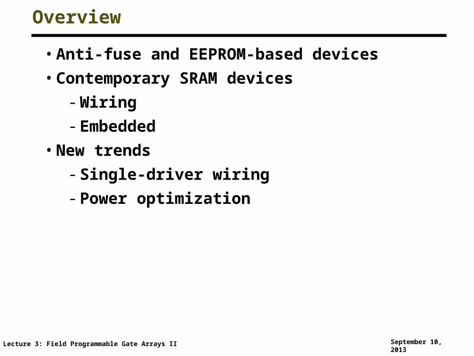
Number of Inputs per Cluster
• Lots of opportunities for input sharing in large clusters (Betz – CICC’99)
• Reducing inputs reduces the size of the device and makes it faster.
• I = K/2 * (N + 1)
Lecture 3: Field Programmable Gate Arrays II September 10, 2013
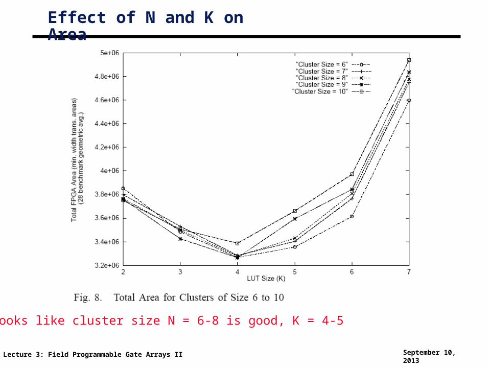
Effect of N and K on Area
Looks like cluster size N = 6-8 is good, K = 4-5

Lecture 3: Field Programmable Gate Arrays II September 10, 2013
Effect of N and K on Area
Intra-cluster area
Lecture 3: Field Programmable Gate Arrays II September 10, 2013
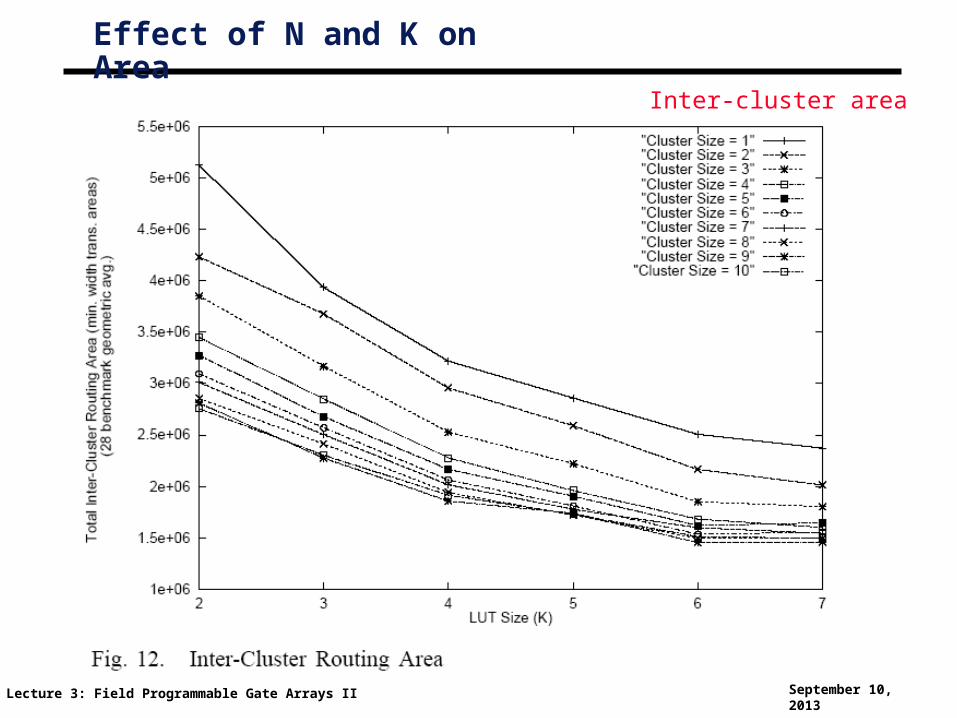
Effect of N and K on Area
Inter-cluster area
Lecture 3: Field Programmable Gate Arrays II September 10, 2013
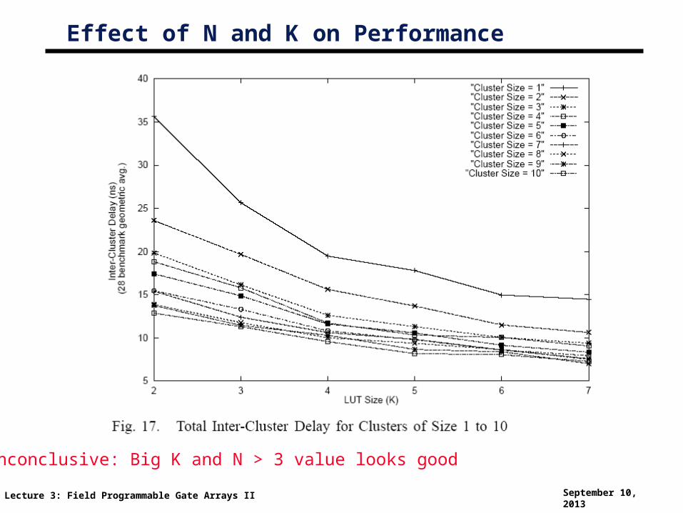
Effect of N and K on Performance
Inconclusive: Big K and N > 3 value looks good
Lecture 3: Field Programmable Gate Arrays II September 10, 2013
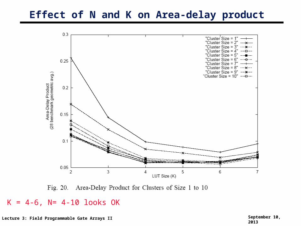
Effect of N and K on Area-delay product
K = 4-6, N= 4-10 looks OK
Lecture 3: Field Programmable Gate Arrays II September 10, 2013
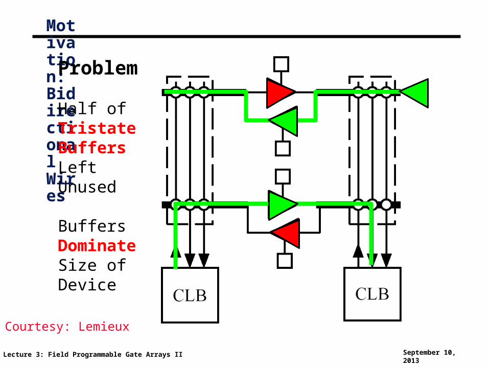
Motivation: Bidirectional Wires
Problem
Half of TristateBuffers LeftUnused
BuffersDominateSize of Device
Courtesy: Lemieux
Lecture 3: Field Programmable Gate Arrays II September 10, 2013
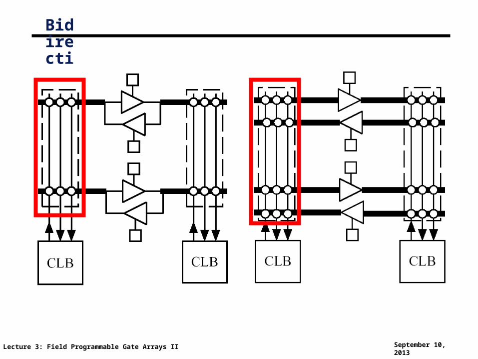
Bidirectional vs Directional
Lecture 3: Field Programmable Gate Arrays II September 10, 2013
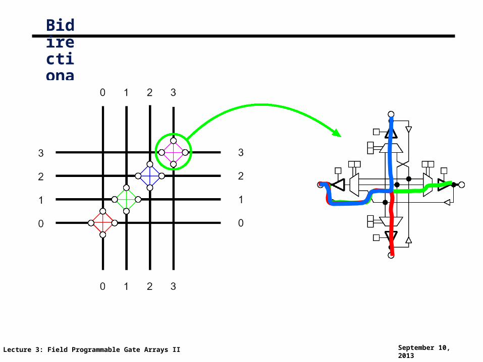
Bidirectional Switch Block

Lecture 3: Field Programmable Gate Arrays II September 10, 2013
Directional versus Bidirectional Switch Block
Switch Block:
Directional has Half as Many Switch
Elements
Lecture 3: Field Programmable Gate Arrays II September 10, 2013
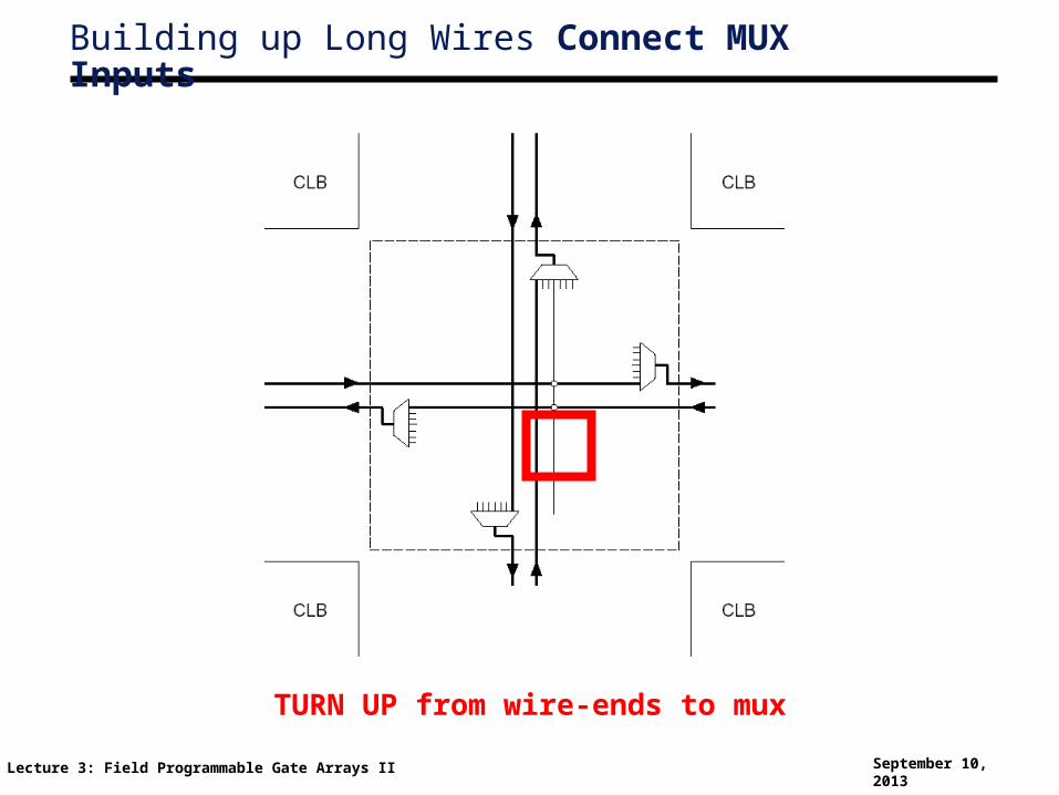
Building up Long Wires Connect MUX Inputs
TURN UP from wire-ends to mux
Lecture 3: Field Programmable Gate Arrays II September 10, 2013
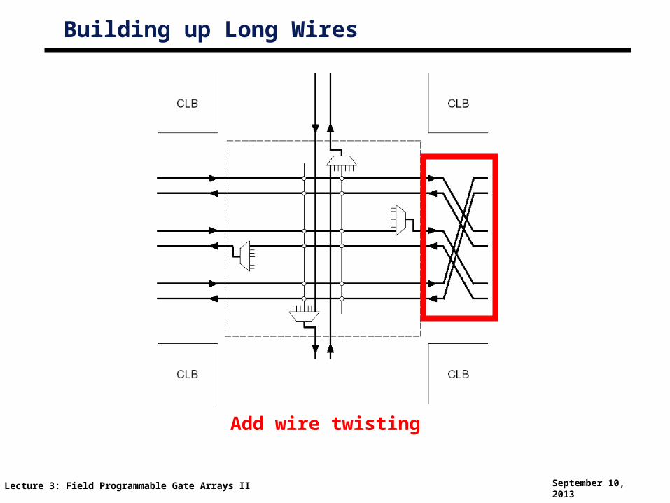
Building up Long Wires
Add wire twisting

Lecture 3: Field Programmable Gate Arrays II September 10, 2013
Directional Wire Summary
° Pros and Cons
• Good
- Potential area savings
- What does this do to CAD tools?
• Bad
- Big input muxes, slower
- Bigger quantum size (2*L)
- Detailed-routing architecture is different(need new switch block)
Lecture 3: Field Programmable Gate Arrays II September 10, 2013
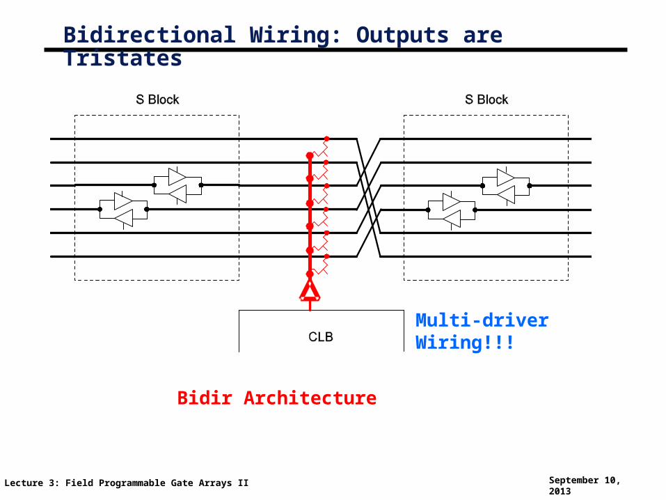
Bidirectional Wiring: Outputs are Tristates
Multi-driverWiring!!!
Bidir Architecture
Lecture 3: Field Programmable Gate Arrays II September 10, 2013
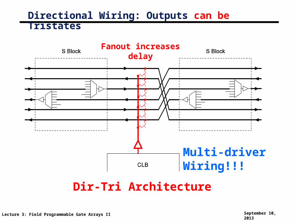
Directional Wiring: Outputs can be Tristates
Dir-Tri Architecture
Multi-driverWiring!!!
Fanout increasesdelay

Lecture 3: Field Programmable Gate Arrays II September 10, 2013
Directional Wiring: Outputs can use switch block muxes
Dir Architecture
Single-driverWiring!!!
New connectivityconstraint
Lecture 3: Field Programmable Gate Arrays II September 10, 2013
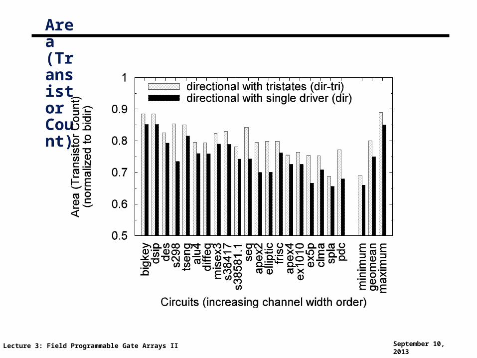
Area (Transistor Count)

Lecture 3: Field Programmable Gate Arrays II September 10, 2013
Delay

Lecture 3: Field Programmable Gate Arrays II September 10, 2013
Area-Delay Product
Lecture 3: Field Programmable Gate Arrays II September 10, 2013
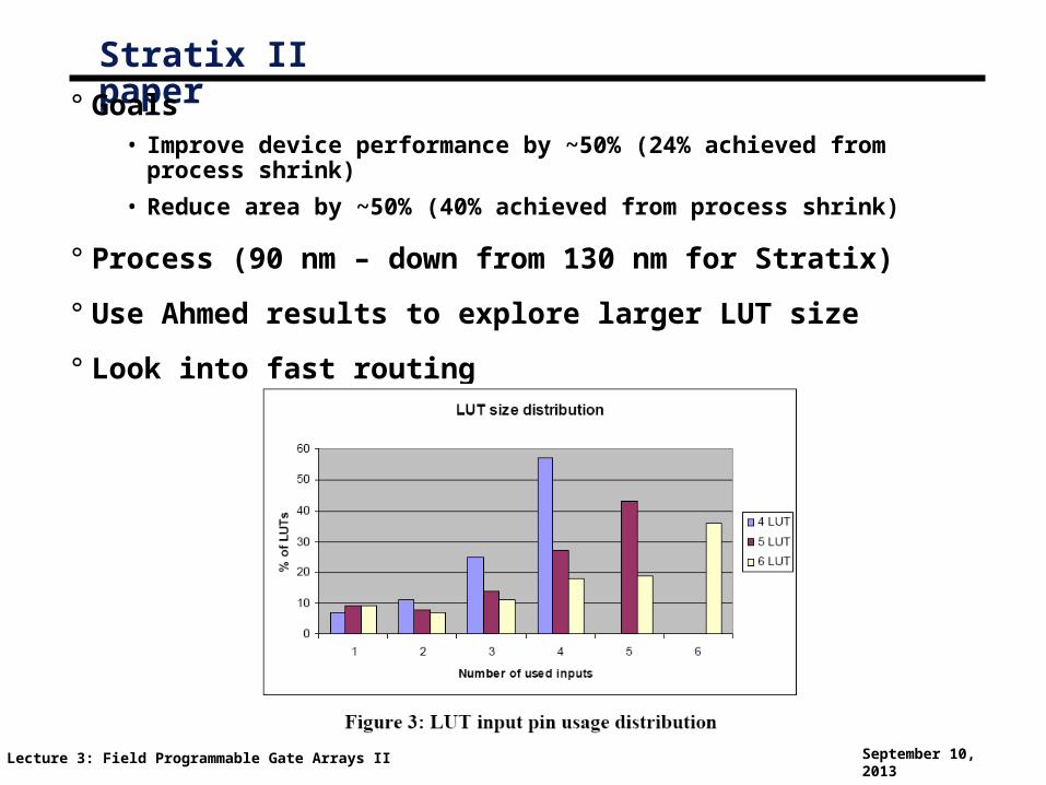
Stratix II paper° Goals
• Improve device performance by ~50% (24% achieved from process shrink)
• Reduce area by ~50% (40% achieved from process shrink)
° Process (90 nm – down from 130 nm for Stratix)
° Use Ahmed results to explore larger LUT size
° Look into fast routing
Lecture 3: Field Programmable Gate Arrays II September 10, 2013
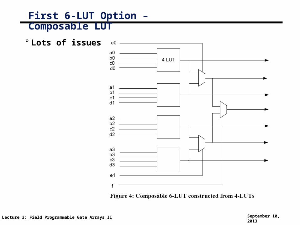
First 6-LUT Option – Composable LUT
° Lots of issues

Lecture 3: Field Programmable Gate Arrays II September 10, 2013
Second 6-LUT Option – Fracturable LUT
° Heading in the right direction
Lecture 3: Field Programmable Gate Arrays II September 10, 2013
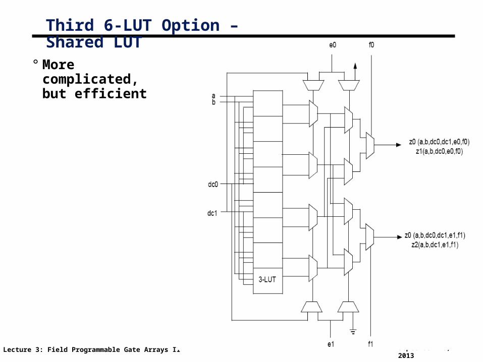
Third 6-LUT Option – Shared LUT
° More complicated, but efficient
Lecture 3: Field Programmable Gate Arrays II September 10, 2013
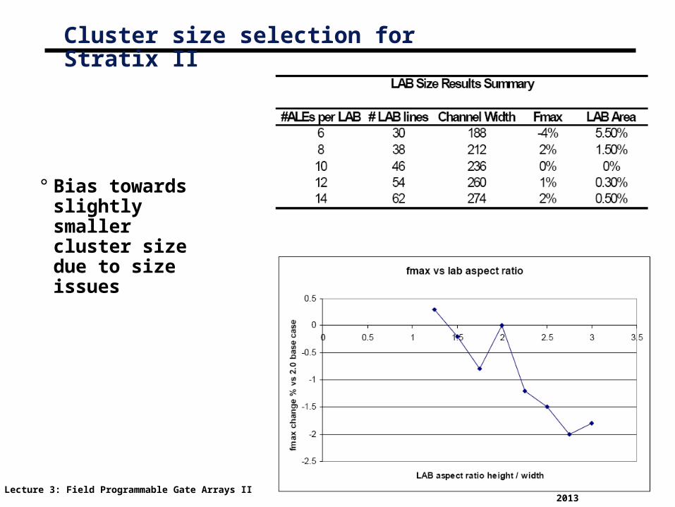
Cluster size selection for Stratix II
° Bias towards slightly smaller cluster size due to size issues
Lecture 3: Field Programmable Gate Arrays II September 10, 2013
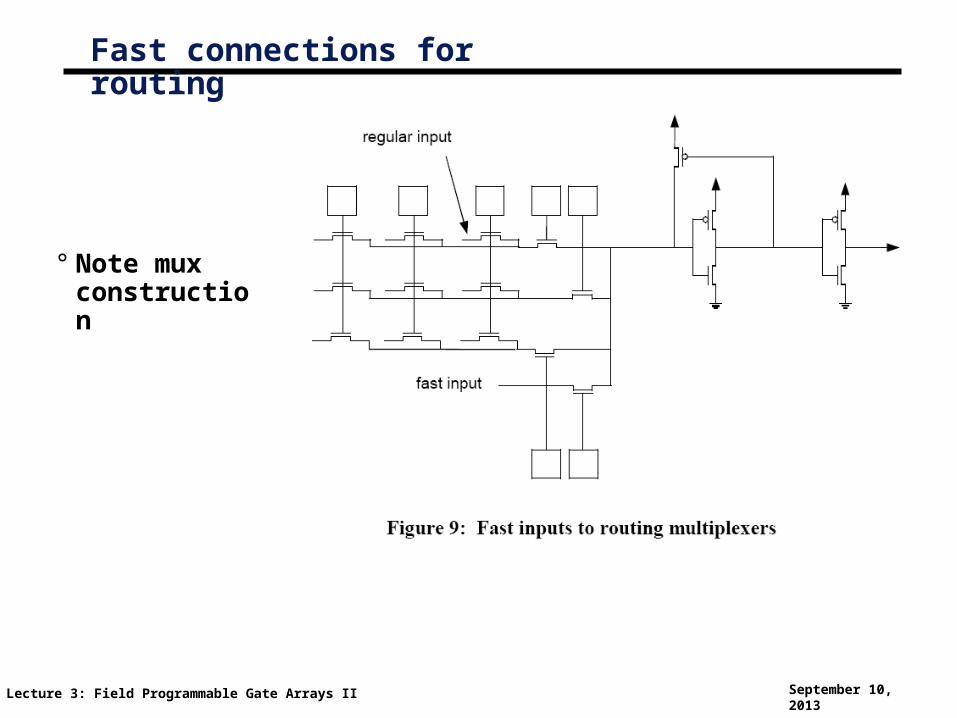
Fast connections for routing
° Note mux construction
Lecture 3: Field Programmable Gate Arrays II September 10, 2013
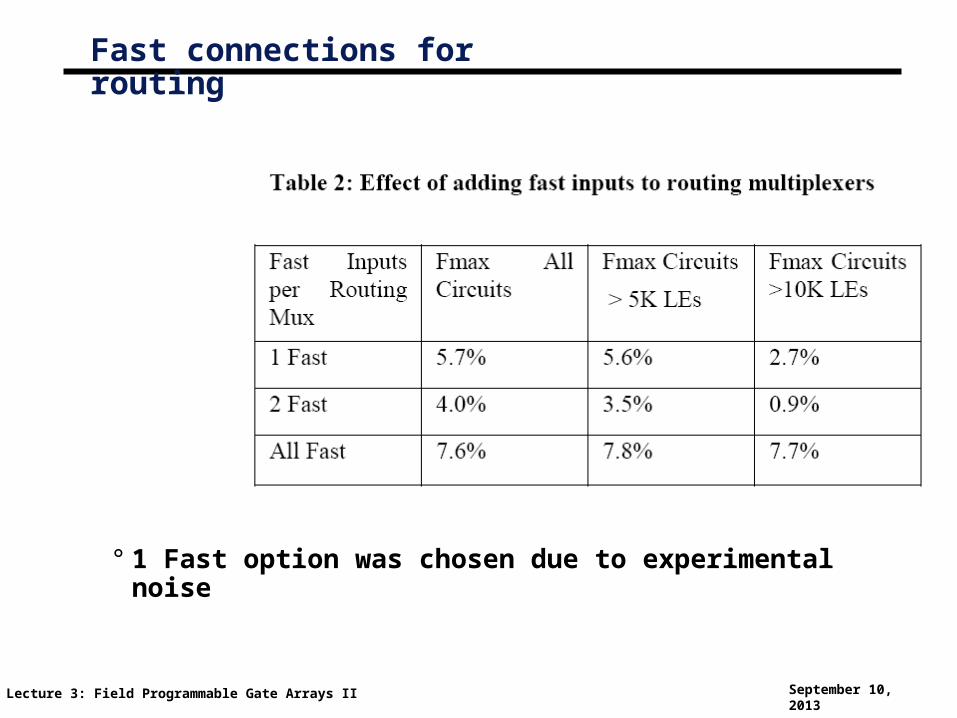
Fast connections for routing
° 1 Fast option was chosen due to experimental noise
Lecture 3: Field Programmable Gate Arrays II September 10, 2013
Summary
• Recent work has reexamined values of N and K inside the cluster
• Performance remains an important issue although power is gaining
• Single-driver wiring reduces area and leads to improved performance
• Commercial architectures are quite advanced
- Rely heavily on CAD tools
Next topic: FPGA placement and routing


![Field Programmable Gate Arrays [Fpga]](https://img.dokumen.tips/doc/110x75/544092dcb1af9f441d8b45c9/field-programmable-gate-arrays-fpga.jpg)