Embed Size (px)
Citation preview

Lecture 20: VLSI CAD Tools
Slides courtesy of Deming Chen, Leslie Hwang, Ashutosh Dhar

Intro. VLSI System Design
Last lecture Alternative design options
– Microprocessor/DSP– Programmable Logic– Gate Arrays and Sea of Gates– Cell-based Design– Full Custom Design– System on a Chip– Intellectual Property (IP)
ECE 425 Slide 2

Intro. VLSI System DesignECE 425 Slide 3
Outline Overview
– Design Languages– CAD Tools
• Design Capture Tools• Synthesis Tools• Verification Tools
– Vivado Design Suite from Xilinx as a case study
Reading– Part of the lecture comes from Text 14.4

Intro. VLSI System DesignECE 425 Slide 4
Design Systems As we have seen, a design system is a set of computer-aided design
(CAD) tools, used to simplify the design and verification tasks.

Intro. VLSI System DesignECE 425 Slide 5
Design Flow Design flow is a set of procedures designers progress from
specification for a chip to the final chip implementation in error-free way
Structural level: gates and registers
Synthesis: transformation to physical (layout) description
RTL: logic and memory elements
ASIC design: flows partitioned between different EDA companies
Behavioral level: operation of the system without implementation

Intro. VLSI System DesignECE 425 Slide 6
Design Languages
A design can be described at different levels of abstraction (high-low):– Architectural level– Finite State Machine level– Logic level– Symbolic level, e.g., PLA– Transistor, or switch level– Sticks level– Mask level

Intro. VLSI System DesignECE 425 Slide 8
Architectural Level Procedural (Architectural Level) Languages
– Primitives are functions and variables– Gives an algorithmic description of the design
• Important special case is Register Transfer Languages (RTL)
• Registers hold the variables• Arithmetic units perform the operations on the variables

Intro. VLSI System DesignECE 425 Slide 9
Logic and FSM Level
Finite State Machine Languages– A symbolic description of states
and state transitions– A behavioral description– Not structural, not geometrical– E.g. microprocessor controller– Can be compiled into PLAs or
logic • The compiler must make
structural and geometrical decisions.

Intro. VLSI System DesignECE 425 Slide 10
Logic Level Logic Languages
– The primitives are logic gates and nodes• Higher level and more versatile than PLA
– Describes logical structure, but no spatial relationships– Can be transformed, or compiled, into a switch language

Intro. VLSI System DesignECE 425 Slide 11
Transistor, Switch and Symbolic Level
Transistor, or Switch, Languages– The primitives are transistors and nodes– Specifies electrical topology– No spatial relationships– Not easily transformed to a geometry
specification– Easily extracted from layout– Suitable for simulation
Symbolic Languages– Slightly higher level than transistors
• E.g. PLA dot diagram– Usually specialized for specific layout styles

Intro. VLSI System DesignECE 425 Slide 12
Stick Level Sticks Languages
– These are virtual or symbolic layout descriptions• A popular example is the LAVA language
– Transistors and vias are represented as points on a grid– Wires are represented as zero-width lines– Gives the relative positions of circuit elements

Intro. VLSI System DesignECE 425 Slide 13
Geometry or Mask Level Geometry Languages
– Use colored rectangles or shapes as their primitives• A popular example is the Caltech Intermediate Form (CIF)
– One can directly fabricate a chip from its description
CIF example

Intro. VLSI System DesignECE 425 Slide 14
CAD Tools Modern design systems use a variety of CAD tools, including: Design-capture tools
– These tools help translate an idea into a high-level design description
Synthesis tools– These tools translate a higher-level description into a lower-
level one Verification tools
– These tools verify that a lower-level implementation is equivalent to a higher-level one
Typically, the design process is not completely automated. Instead, the various CAD tools are used at the designer’s
discretion to facilitate and validate the design tasks. CAD tools need to understand both the language and the
primitives that the language refers to

Intro. VLSI System DesignECE 425 Slide 15
Design Capture Tools
Design-capture tools are the first tools to be used. They provide an interface between what the designer
has in mind and the high-level design description. There are two general methods of design capture
Textually: body of code Schematically: graphical

Intro. VLSI System DesignECE 425 Slide 16
Hardware Description Languages
Many design systems allow designers to use a free mix of code and diagrams.
In general, schematics are easier to understand, but HDLs may be easier to modify.
Textual design specification is in terms of a Hardware Description Language (HDL).
HDLs allow one to specify the circuit structure and behavior.
The most popular (and standardized) HDLs– Verilog, SystemVerilog– VHDL

Intro. VLSI System DesignECE 425 Slide 17
Schematic Capture Tools Schematic capture tools allow the user to graphically
draw and connect components. A collection of components are grouped into a
module, for which a symbol may be defined. This symbol may be used in another module,
hierarchically, throughout the design.

Intro. VLSI System DesignECE 425 Slide 18
An Example for Schematic Capture
Here’s a typical module schematic and the corresponding icon:

Intro. VLSI System DesignECE 425 Slide 19
Layout Editors Design capture tools are typically used at the RTL
and logic levels. They can also be used at the lowest (layout) and
highest (architecture) levels. Layout editors accept a
design description in terms of shapes, sizes, and attributes.
They typically interface with a Design Rule Checking program and an extraction program.

Intro. VLSI System DesignECE 425 Slide 20
Synthesis Tools Effectively, these tools transform the design specification from
the abstract (high-level) to the concrete (low-level)– For example: given a Boolean function, find a “good” choice
and arrangement of logic gates that implement it.– The solution to this problem is called logic synthesis.
As the name implies, synthesis tools build the design.

Intro. VLSI System DesignECE 425 Slide 21
High-level (or Behavioral) Synthesis Design Flow Given a description of the behavior of the design, a behavioral compiler
should:– Schedule the sequence of operations to be performed– Allocate hardware resources to these operations– Create microcode and/or control logic
This process is technology-independent and is generally very difficult to perform optimally.
High-level Synthesis
High-level Verification

Intro. VLSI System DesignECE 425 Slide 22
High-Level (Behavioral) Synthesis
This process is trying to optimize circuit area, power, and delay, etc.
Such high-level synthesis has gained popularity especially for FPGA designs– bit-serial digital filters– deep neural networks– signal-processing architectures
In more general cases, manual synthesis usually still gives better results especially for ASIC designs.
An increasing important area due to growing design complexity
Tool suppliers: Cadence Design Systems, Mentor Graphics, Altera, Xilinx, etc.
Intro. VLSI System DesignECE 425 Slide 23
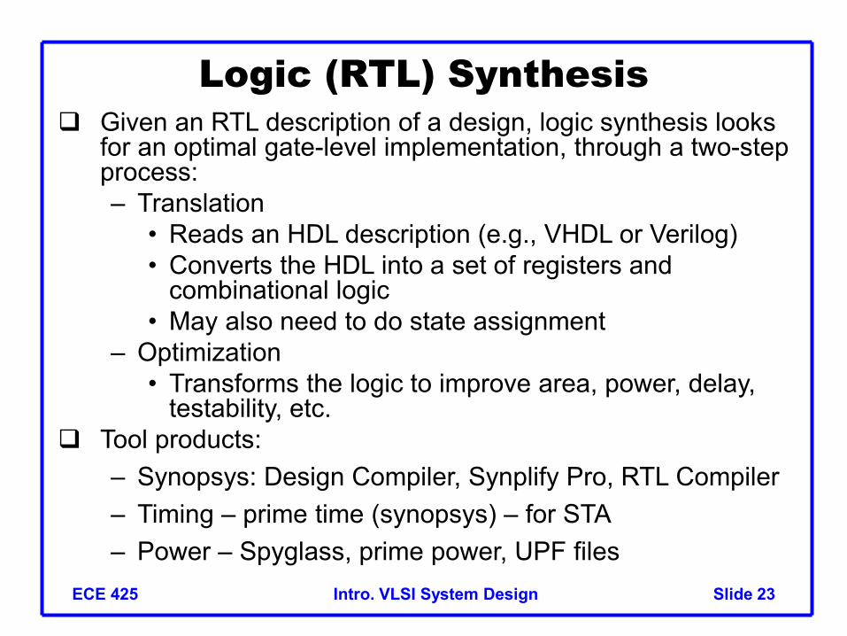
Logic (RTL) Synthesis Given an RTL description of a design, logic synthesis looks
for an optimal gate-level implementation, through a two-step process:– Translation
• Reads an HDL description (e.g., VHDL or Verilog)• Converts the HDL into a set of registers and
combinational logic• May also need to do state assignment
– Optimization• Transforms the logic to improve area, power, delay,
testability, etc. Tool products:
– Synopsys: Design Compiler, Synplify Pro, RTL Compiler– Timing – prime time (synopsys) – for STA– Power – Spyglass, prime power, UPF files

Intro. VLSI System DesignECE 425 Slide 24
RTL Synthesis The solution methods are well understood and mature. It
involves two phases:– A technology-independent phase
• The logic is optimized using algebraic and/or Boolean techniques
– A technology-mapping phase• Specific library cells are chosen to implement the
optimized
High-level Synthesis
High-level Verification

Intro. VLSI System DesignECE 425 Slide 25
Layout Synthesis Finally, the technology-mapped circuit is translated to a layout. More optimization is required at this point to choose a layout that has
a small area and is easily routable. Two stages technique: Placement
– Decide where to place the cells to improve area and routability
Routing– Decide how to route the metal wires
between the cells– Global router
• used during placement to assess routability
– Detailed router• places actual geometry and
completes connection

Intro. VLSI System DesignECE 425 Slide 26
Floorplanning At the architectural level, schematic capture allows
one to study the optimal arrangement of blocks within a chip.
This, so-called Floorplanning, is done in order to minimize area or maximize speed.
Floorplanning can be done by hand if not many blocks; otherwise, simulated annealing is usually the preferred algorithm for floorplanning.

Intro. VLSI System DesignECE 425 Slide 27
Floorplaning Example For instance, it is clear that this floorplan can be improved by
flipping module D around the vertical axis:
Intro. VLSI System Design
Verification
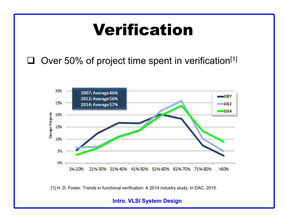
Over 50% of project time spent in verification[1]
[1] H. D. Foster. Trends in functional verification: A 2014 industry study. In DAC, 2015.

Intro. VLSI System DesignECE 425 Slide 29
Verification Tools It is always important to verify equivalence between different
levels of the design.
• Simulation tools• Timing verification tools• Formal verification tools
Intro. VLSI System DesignECE 425 Slide 30
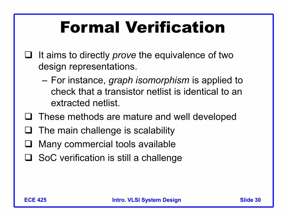
Formal Verification It aims to directly prove the equivalence of two
design representations.– For instance, graph isomorphism is applied to
check that a transistor netlist is identical to an extracted netlist.
These methods are mature and well developed The main challenge is scalability Many commercial tools available SoC verification is still a challenge

Intro. VLSI System DesignECE 425 Slide 31
Formal Verification At a slightly higher level, Boolean equivalence is
used to check if a gate-level implementation performs required Boolean function, as specified in the RTL description (equivalence checkers).– Binary Decision Diagrams (BDDs) extracted and
compared.

Intro. VLSI System DesignECE 425 Slide 32
Formal Verification Model checking is used to verify specified properties of a
design At the highest level, theorem proving techniques are used to
prove a system correct, as in proving a mathematical theorem to be correct.– Unable to pinpoint errors in incorrect designs.– Difficult for non-experts to operate effectively.– Not well developed and the topic of ongoing research.

Intro. VLSI System DesignECE 425 Slide 33
Simulation Tools Simulators are probably the most often used design
tools. A simulator uses mathematical models to represent
the behavior of circuit components. Given specific input signals, the simulator solves for
the signals inside the circuit. Simulators come in a wide variety depending on the
level of accuracy and the simulation speed desired:– circuit simulation– switch-level simulation– logic simulation– functional simulation

Intro. VLSI System DesignECE 425 Slide 34
Interactive design environment and simulators: – Cadence Design Systems: NC-
Verilog(ECE425)/SystemC/VHDL or Desktop Verilog/VHDL
– Synopsys: VCS– Mentor Graphics: ModelSim– Aldec: ActiveHDL– SPICE
Simulation Tools

Intro. VLSI System DesignECE 425 Slide 35
MP3 Automation Tools Logic Synthesis: Schematic automation
– Tool: Design Vision by Synopsys
Place & Route: Layout automation– Tool: Encounter by Cadence– Industry-standard file formats
• Floorplan: DEF format (.def)• Layout: GDSII format (.gds)
Convert from Convert toBehavioral HDL Schematic, structural RTL
controller.v controller_synth.v
Convert from Convert toSynthesized RTL Layoutcontroller_synth.v controller.def, controller.gds

Intro. VLSI System Design
Case Study of Xilinx Vivado Design Tools
SDSoC HLS Logic Synthesis Placement and Routing Bitstream generation
ECE 425 Slide 36
Intro. VLSI System Design
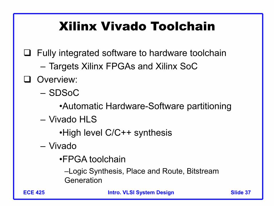
Xilinx Vivado Toolchain
Fully integrated software to hardware toolchain– Targets Xilinx FPGAs and Xilinx SoC
Overview:– SDSoC
•Automatic Hardware-Software partitioning– Vivado HLS
•High level C/C++ synthesis– Vivado
•FPGA toolchain–Logic Synthesis, Place and Route, Bitstream Generation
ECE 425 Slide 37

Intro. VLSI System Design
Example: Zynq System
Xilinx accelerated system: Zynq SoC– ARM processor +
FPGA ARM processor for
control and OS FPGA
– Custom hardware (Recall ECE385)
– Build an “accelerator” on FPGA
ECE 425 Slide 38

Intro. VLSI System Design
Example: Vector Addition
Traditional Flow:
ECE 425 Slide 39
main() {readData(a,b,c)preprocessData()
for(i=0 to N)c[i]=a[i]+b[i]
checkData()}
Find critical code
Accelerator Architecture Design
Design HW-SW Communication
Develop RTL Develop Software
Profile Application
Partition HW/SW
Synthesis, P&R Compile, Link
Implement System

Intro. VLSI System Design
HW-SW Partitioning
Hard problem– Time consuming to do manually
Common approach– Profile application– Characterize compute operations– Characterize communication/memory
Xilinx SDSoC– Automate HW-SW partitioning– Targets Zynq SoC platforms (not generic FPGA)
ECE 425 Slide 40

Intro. VLSI System Design
Xilinx SDSoC “Software Defined SoC” Development environment for
software/embedded designers IDE that helps automate
HW/SW co-design– Includes profiling tools– Performance estimation
tools Includes a library of
communication/data movers– Simple, Scatter-gather, 2D
DMA System-wide performance
optimization For more:
https://youtube/SiOXTJ8IkJAECE 425 Slide 41
[1] Xilinx UG1028: SDSoC Environment User Guide

Intro. VLSI System Design
High Level Synthesis
Given partitioned HW/SW, how to design and implement accelerator?– RTL development takes time– Architecture exploration
HLS: High level language to Hardware– Speedup development time– Given code (C/C++) generates control and datapath
Explore different architecture tradeoffs– Datapath latency– Datapath width– Bandwidth requirements
ECE 425 Slide 42

Intro. VLSI System Design
Vivado HLS
Xilinx HLS solution– C/C++ input
Use pragmas to “optimize” design– Design space exploration
Co-simulate hardware with software tests– Speedup design verification
Must write “synthesizable” C/C++ code– Eg. malloc, dynamic memory not allowed– Eg. “printf” doesn't make sense in hardware
ECE 425 Slide 43

Intro. VLSI System Design
Vivado HLS (2)
ECE 425 Slide 44
EditorHLS
Directives ExplorerFile Explorer
Console Display
Intro. VLSI System Design
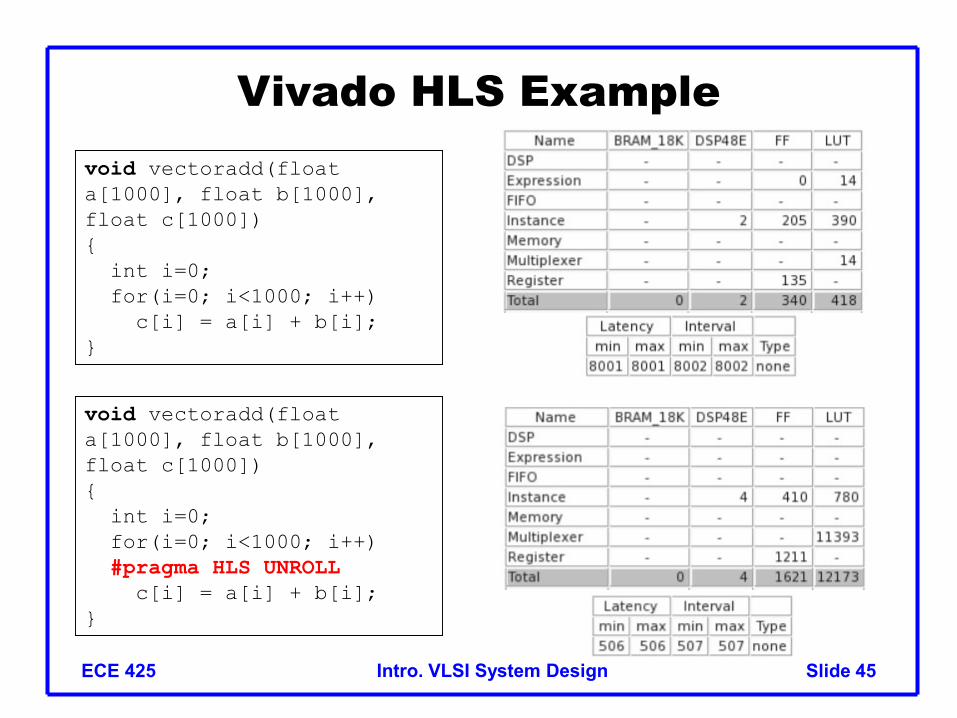
Vivado HLS Example
ECE 425 Slide 45
void vectoradd(float a[1000], float b[1000], float c[1000]){
int i=0;for(i=0; i<1000; i++)
c[i] = a[i] + b[i];}
void vectoradd(float a[1000], float b[1000], float c[1000]){
int i=0;for(i=0; i<1000; i++)#pragma HLS UNROLL
c[i] = a[i] + b[i];}

Intro. VLSI System Design
Vivado
Xilinx toolchain for FPGA design– Design editor
•RTL•IP integration
– Logic Synthesis•Elaboration•Synthesis•Mapping
– Place and Route– Bitstream generator
ECE 425 Slide 46
Fully Automated

Intro. VLSI System Design
Vivado
ECE 425 Slide 47
module accumulator(input clk,input rst,input [7:0] in,output [31:0] out);
reg [31:0] acc;assign out = acc;
always @(posedge clk)begin
if(rst)begin
acc <= 0;endelsebegin
acc <= acc+in;end
end endmodule
RTL Elaboration- Elaborate RTL design to logic units

Intro. VLSI System Design
Vivado
Given Elaborated design– Synthesize to netlist– Logic mapping
•“Map” logic elements to Flip-Flops, LUTs, BRAM and DSP units
Synthesis solution can be “optimized”– Power, Area, Timing
Place and Route– Cluster LUTs, FFs etc into logic blocks
•Determined by FPGA architecture– Connect “logic blocks” using fixed routing resources
Fully automated
ECE 425 Slide 48

Intro. VLSI System Design
Vivado
Example Placed&Routed Design– Blue regions are
the design mapped to the FPGA
ECE 425 Slide 49

Intro. VLSI System Design
Vivado
How do we program the FPGA?– Bitstream
FPGA relies on “configuration memory”– Programming FPGA requires writing to the memory– “Bitstream” contains configuration bits + additional
data– Unique to FPGA architecture
Vivado generates bitstream from placed and routed design– Provides an interface to “burn” the FPGA with the
bitstream too
ECE 425 Slide 50

Intro. VLSI System Design
Summary Design Languages
– The most popular is RTL– High-level languages gaining popularity
CAD Tools– Design Capture Tools– Synthesis and physical design (the main steps)– Verification Tools (need better tools)
Vivado Design Suite– Very strong in terms of system-level features
Next lecture– High-Level Synthesis– https://www.youtube.com/watch?v=5lYq8_bqAcI
ECE 425 Slide 51