Embed Size (px)
Citation preview

1
IIT Madras - C.P. Ravikumar 1
Lecture #2Solving the Interconnect
Problems in VLSI
C.P. Ravikumar
IIT Madras - C.P. Ravikumar 2
Interconnect Problems
l Interconnect delay has become more important than gate delays after 130nm technology node was introduced
l How does this impact the design flow?l “Timing Closure” problem

2
IIT Madras - C.P. Ravikumar 3
Interconnect delays
Source - ITRS
IIT Madras - C.P. Ravikumar 4
Need for CommunicationNeed for Communication--centric centric Design FlowDesign Flow
l Communication is THE most critical aspect affecting system performance
l Communication architecture consumes upto 50% of total on-chip power
l Ever increasing number of wires, repeaters, bus components (arbiters, bridges, decoders etc.) increases system cost
l Communication architecture design, customization, exploration, verification and implementation takes up the largest chunk of a design cycle
Communication Architectures in today’s complex systems significantly affect performance, power, cost and time-to-market!
Communication Architectures in today’s complex systems significantly affect performance, power, cost and time-to-market!
4© 2008 Sudeep Pasricha & Nikil Dutt

3
IIT Madras - C.P. Ravikumar 5
SolutionsMaterial with better ρ
l Moving to copper interconnect
l Trenches are created in the underlying silicon oxide insulating layer where the metal is desired.
l A thick coating of copper deposited – overfills the trenches
l Chemical-mechanical Polishing used to remove the copper to the level of the top of the insulating layer
l Barrier metal needed to prevent spreading
2.82 x 10⁻⁸ ΩmAl
1.72 x 10⁻⁸ ΩmCu
IIT Madras - C.P. Ravikumar 6
Interconnect Reliability
l Metal Migration (EM)l Can result in long-term failure of interconnectsl Reliability problem in integrated circuits – Copper
is better than Aluminum

4
IIT Madras - C.P. Ravikumar 7
SolutionsReduce interconnect resistance
l Increase metal thicknessl What side effects does
this cause?
HWLR ρ
=
IIT Madras - C.P. Ravikumar 8
Solutions to Crosstalk Problem:Reduce parasitic capacitance
l Low-k Dielectricl Silicon Dioxide has a relative permittivity of 3.9l Materials research has yielded dielectrics with lower
permittivityl Flourine doped SiO2 – 3.5l Carbon doped SiO2 – 3.0
l Crosstalk analysisl Crosstalk Delay and Crosstalk Failure
l Increase metal separation (selectively)l Crosstalk aware placement & routing

5
IIT Madras - C.P. Ravikumar 9
Interconnect Estimation
l Logic Synthesis tools need to estimate interconnect lengths and wire delaysl Statistical Wire Load Model (WLM)
l Physical Synthesis tools perform placement and routing concurrently with synthesis
IIT Madras - C.P. Ravikumar 10
Interconnect Delay Calculation
l Lumped and Distributed Delay Models

6
IIT Madras - C.P. Ravikumar 11
Elmore Delay Model
Vin Vout
R1
C1
R2
C2
1 2Ri-1
Ci-1
i-1Ri
Ci
iRN-1
CN-1
N-1RN
CN
N
∑∑∑∑====
==i
jj
N
ii
N
ijj
N
iiN RCCR
111τ
IIT Madras - C.P. Ravikumar 12
Example
l Assume N segments, each with resistance rand capacitance c
The Elmore Delay can be further extended for interconnects with tree topology

7
IIT Madras - C.P. Ravikumar 13
Elmore Delay for RC Tree
l Delay at a node j = Σk (Ck Rjk) l Rjk is the sum of all resistances that are common to the path from
the source to node j and the path from source to node kl Delay at node 1 = C1 (R1) + C2 (R1) + C3 (R1)l Delay at node 2 = C1 (R1) + C2 (R1+R2) + C3(R1)l Delay at node 3 = C1 (R1) + C2 (R1) + C3 (R1+R3)
IIT Madras - C.P. Ravikumar 14
When should inductance be When should inductance be considered?considered?
ó Length criteria for including inductance in interconnect model
14© 2008 Sudeep Pasricha & Nikil Dutt

8
IIT Madras - C.P. Ravikumar 15
Reducing Interconnect DelayRepeater Insertion
l Where should the buffers be inserted?
l What are the sizes of the buffers?
IIT Madras - C.P. Ravikumar 16
Interconnect Delay with repeatersl Consider a wire of length L, divided into N sectionsl Assume that there are N repeaters, one at the
beginning of each sectionl Assume that the W/L ratio for a unit-sized driver is β
l Assume that all drivers are of size Ml Model for any section must includel Self-resistance of the repeaterl Self-capacitance of the repeaterl π-model of the Interconnect segment of length L/Nl Load capacitance presented by the subsequent repeater

9
IIT Madras - C.P. Ravikumar 17
RC-model for one segmentR1 = Rd/M
C1 = Cd M (1+β) + Cint L/(2N) C2 = Cg M (1+β) + Cint L/(2N)
R2 = Rint L/N
Elmore Delay at the output of the segment is:
tsegment = R1 C1 + (R1+R2)C2
Total delay of the wire with repeaters = N tsegment
Differentiate the total delay expression w.r.t. N and set it to 0 ; solve for N to get NoptDifferentiate the total delay expression w.r.t. M and set it to 0; solve for M to get Mopt
IIT Madras - C.P. Ravikumar 18
Signal Routingl Synchronous digital circuits that use edge-triggered
flip-flopsl Concept of setup delayl Period of the clock = Tl T > tclk-q of launch flop + Path delay from Qlaunch to Dcapture + tsetup of
capture flop
l Path Delay in deep submicron technologies depends onl Gate Delay (which is a function of P, V, T)l Interconnect Delay

10
IIT Madras - C.P. Ravikumar 19
Logic Synthesis and Physical Designl Before 130nm technology, it was possible to
separate logic synthesis and physical designl Interconnect delays were not as big a component as gate
delay before 180nml Estimating interconnect delay through statistical wireload
model was reasonably accurate in 180nm technologyl Timing Closure problems in 130nm technology and
beyondl Unable to predict interconnect delays accurately without
knowledge of placement and routing informationl “Physical Synthesis” performs logic synthesis + physical
design simultaneously – tools are more complex
IIT Madras - C.P. Ravikumar 20
Performance-directed Placement and Routing
l Delays estimated in logic synthesis can be fed as constraints to physical design tools
l Early physical design tools mainly focussedon minimizing TOTAL wire lengthl There were constraints on routing congestion
l Placement and routing tools today accept timing constraints

11
IIT Madras - C.P. Ravikumar 21
Routing Treesl A multiple-pin net (wire) is
routed as a treel Minimum-length Rectilinear
Spanning Treel Create an MST using
Euclidean distance as a measure
l Convert the edges to Manhattan routes
l Minimum-length Rectilinear Steiner Treel Introduce Steiner points
l Example shows a 4-pin netl E.G. One gate driving 3 other
gates
10 units of wire
8 units of wire
IIT Madras - C.P. Ravikumar 22
Wireload modell Get an estimate of wirelength at logic synthesis
stagel Model wire-length as a function of fan-outl “Statistical Wireload model”l Collect chip data and create a correlation between fanout
and wirelength

12
IIT Madras - C.P. Ravikumar 23
Driver SizingDriver Sizingl Transistor sizing techniques aim to lower delayl Wider transistors have a few advantages but also
several disadvantagesl + produce more currentl + reduce charge time of load capacitancel – have greater physical areal – have larger gate capacitancel – increased circuit area and power
23© 2008 Sudeep Pasricha & Nikil Dutt
IIT Madras - C.P. Ravikumar 24
Wire SizingWire Sizingl Width of an interconnect affects the power characteristics and
propagation delayl Consider a CMOS inverter driving an RC interconnect linel Simple first order model of delay
24© 2008 Sudeep Pasricha & Nikil Dutt

13
IIT Madras - C.P. Ravikumar 25
Wire SizingWire Sizingl Increasing the driver transistor width reduces Rtr
l decreasing the circuit delayl trading off circuit power and area for higher speed
l Increasing the width of the interconnect to reduce Rint does not significantly reduce the delay caused by the RC interconnect impedance l since decrease in wire resistance is offset by
increase in wire capacitance
25© 2008 Sudeep Pasricha & Nikil Dutt
IIT Madras - C.P. Ravikumar 26
Wire SizingWire Sizing
lDynamic power increases with width since line capacitance is greaterlAs line inductance-to-resistance ratio
increases with wider lines, short-circuit power decreases due to reduction in signal transition time
26© 2008 Sudeep Pasricha & Nikil Dutt

14
IIT Madras - C.P. Ravikumar 27
3-D ICsl With shorter interconnects in
3D ICs, switching energy and cycle time are expected to be reduced
l Take advantage of multiple layers in routing critical paths
IIT Madras - C.P. Ravikumar 28
Types of interconnects
l Signal carriersl Carry data and control signals
l Clock carriersl Power and Ground

15
IIT Madras - C.P. Ravikumar 29
Clock Tree Constructionl Synchronous circuits require that (ideally) all flip-
flops toggle at the same timel Interconnect Delays along the clock line result in
clock skewl Clocks are often designed as H-tree to balance the
skew from source to sinksl T > skew + tclk-q of launch flop + Path delay from Qlaunch to Dcapture +
tsetup of capture flop
l When number of IP increases, maintaining the synchronous paradigm is a challengel Globally Asynchronous, Locally Synchronous
IIT Madras - C.P. Ravikumar 30
Signal Carriers
l Point-to-point connectionsl One source of data and one sink
l Sometimes, we may have multiple sources of data and multiple sinksl Example – multiple CPUs / multiple memories
l Bus is a way to share data pathsl Reduces interconnect areal As we increase the number of sources/sinks,
communication latencies increase
16
IIT Madras - C.P. Ravikumar 31
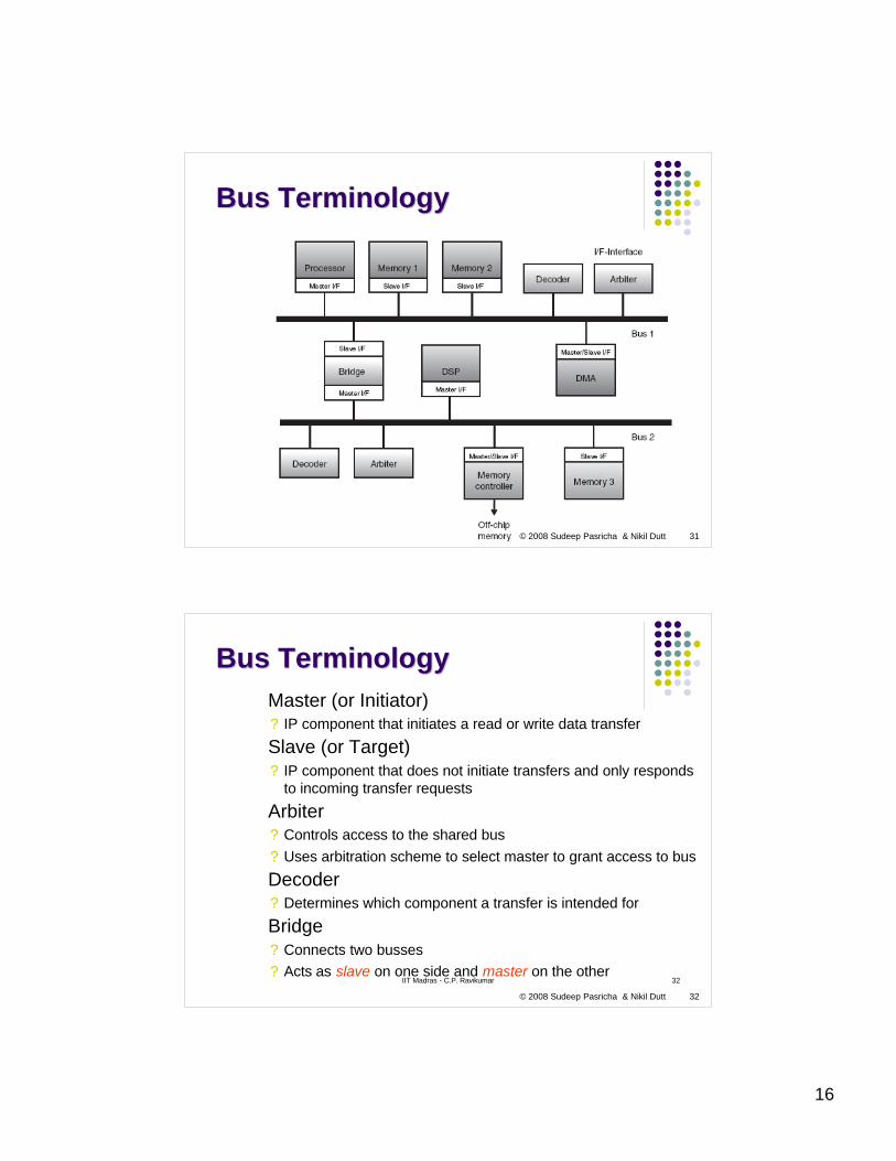
Bus TerminologyBus Terminology
31© 2008 Sudeep Pasricha & Nikil Dutt
IIT Madras - C.P. Ravikumar 32
Bus TerminologyBus Terminology
© 2008 Sudeep Pasricha & Nikil Dutt 32
ó Master (or Initiator)? IP component that initiates a read or write data transfer
ó Slave (or Target)? IP component that does not initiate transfers and only responds
to incoming transfer requests ó Arbiter
? Controls access to the shared bus? Uses arbitration scheme to select master to grant access to bus
ó Decoder? Determines which component a transfer is intended for
ó Bridge? Connects two busses? Acts as slave on one side and master on the other

17
IIT Madras - C.P. Ravikumar 33
Bus Physical StructureBus Physical Structure
l tri-state buffer based bidirectional signals
l Commonly used in off-chip/backplane busesl + take up fewer wires, smaller area footprintl - higher power consumption, higher delay, hard to debug
33© 2008 Sudeep Pasricha & Nikil Dutt
IIT Madras - C.P. Ravikumar 34
Bus Physical StructureBus Physical Structure
lMUX based signals
34© 2008 Sudeep Pasricha & Nikil Dutt
ó Separate read, write channels

18
IIT Madras - C.P. Ravikumar 35
Bus interconnects
l Routing congestionl Example – a single controller for a large number
of data path elementsl Higher Bus capacitance implies higher bus
power and delayl Crosstalk may result in data errorsl Data encoding techniques exist to reduce such
errors and the switching activity on the bus lines
IIT Madras - C.P. Ravikumar 36
Bus crosstalkl Concept of a victim and an aggressorl In a bus with multiple wires, a single wire may have
multiple aggressorsl Shielding can eliminate the crosstalk between two
wiresl Extra area
l An entire metal layer is sometimes used in between two metal layers to shield wires in the two layers from crosstalk
l Encoding of data can be used to achieve a similar effect


![[IJET V2I5P22] Authors: Gangasani Ravikumar Reddy, M.Suneetha](https://img.dokumen.tips/doc/110x75/587096461a28ab412b8b684d/ijet-v2i5p22-authors-gangasani-ravikumar-reddy-msuneetha.jpg)