Embed Size (px)
Citation preview

1
WelcometomysecondyearcourseonDigitalElectronics.YouwillfindthattheslidesaresupportedbynotesembeddedwiththePowerpointpresentations.Allmyteachingmaterialsarealsoavailableonthecoursewebpage:www.ee.ic.ac.uk/pcheung/teaching/ee2_digital/.TheQRcodehereprovidesashortcuttogotothecoursewebpage.Iwillbeupdatingthenotes,thelaboratoryinstructionsandtutorialproblemsheetseachweekafterthelectures.AllmylectureswillberecordedwithPanopto.Therecordingswillalsobeuploadassoonaspossibleafterthelectures.
Thecourseconsistsofabout16hourslecturesinterleavedwith6problemsolvingclasses.ThesewillbeheldonTuesday4pmto6pmandThursday12noonto1pmstartingfrom18th ofOctober.SinceIhavetobeawayinthefirstteachingweekonCollegebusiness,Iwillalsohaveacatch-uplectureonFriday21st ofOctoberat4pm.
ThiscoursefollowsonfromthefirstyearDigitalElectronicsIcourse.Unlikethefirstyearcoursewhereallgatesandflip-flopsareassumedtoexhibitidealbehaviour,thiscoursewillteachyouaboutreal-lifecircuits.
Digitalcircuitsareubiquitous.Forexample,therearemoreelectronicmodulesincarsthesedaysthanmechanicalsystems.Amobilehasmoretransistorsthanhumanaliveonearth,andmostofthesetransistoraredigital,i.e.workingason-offswitches.ThereforethissecondyeardigitalelectronicscourseisfundamentaltoanyEEEorEIEeducation.

2
Lastyearyoulearnedaboutimplementingdigitalcircuitsusinggatessuchastheoneshownhere.YoucanstillbuythischipwithFOURNANDgatesinonepackageandthisisknownasdiscretelogic.Wegenerallydonotusetheseanymore.Itisslow,expensive,consumeslotsofenergyandveryhardtouse.
Nevertheless,itisgoodtolearnaboutNANDandNORgatesbecause,usingDeMorgan’stheorem,youcouldintheorydesignandimplementanInteli7microprocessorusingusetwoinputNANDorNORgatesalone. NANDorNORgatesthereforecouldberegardedasthebuildingblockofalldigitalcircuits.Similarly,youcouldintheorybuildacarusingonlybasicLegoblocks.Unfortunatelysuchacarwouldnotbeverygood.
3
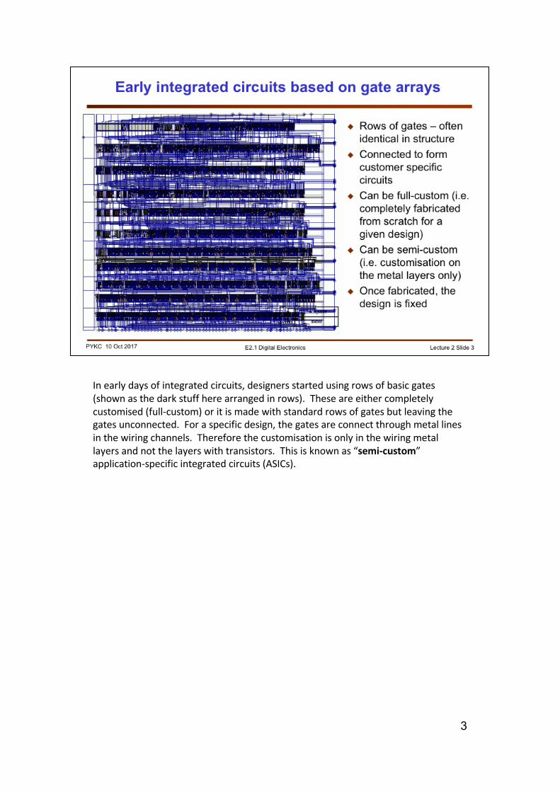
Inearlydaysofintegratedcircuits,designersstartedusingrowsofbasicgates(shownasthedarkstuffherearrangedinrows).Theseareeithercompletelycustomised (full-custom)oritismadewithstandardrowsofgatesbutleavingthegatesunconnected.Foraspecificdesign,thegatesareconnectthroughmetallinesinthewiringchannels.Thereforethecustomisation isonlyinthewiringmetallayersandnotthelayerswithtransistors.Thisisknownas“semi-custom”application-specificintegratedcircuits(ASICs).

4
Ofcourseyoucanalsocustomise everything– eachtransistorandeachwiringconnectedinafull-custommanner.HereisthelayoutofInteli7microprocessor(with4cores).Designingsuchacircuitisveryexpensive,highlyrisky,andoncedesigned,itcannotbechangedeasily.
Mostapplicationsinelectronicindustrycannotaffordtoembarkonsuchadesign.ThisdrivestheriseoftheFieldProgrammableGateArray.
5
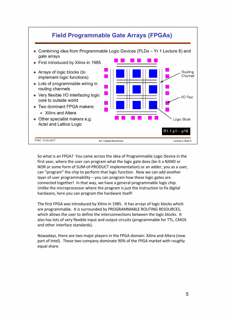
SowhatisanFPGA?YoucameacrosstheideaofProgrammableLogicDeviceinthefirstyear,wheretheusercanprogramwhatthelogicgatedoes(beitaNANDorNORorsomeformofSUM-of-PRODUCTimplementation)oranadder,youasauser,can“program” thechiptoperformthatlogicfunction.Nowwecanaddanotherlayerofuserprogrammability– youcanprogramhowtheselogicgatesareconnectedtogether!Inthatway,wehaveageneralprogrammablelogicchip.Unlikethemicroprocessorwheretheprogramisjusttheinstructiontofixdigitalhardware,hereyoucanprogramthehardwareitself!
ThefirstFPGAwasintroducedbyXilinxin1985.Ithasarraysoflogicblockswhichareprogrammable.ItissurroundedbyPROGRAMMABLEROUTINGRESOURCES,whichallowstheusertodefinetheinterconnectionsbetweenthelogicblocks.Italsohaslotsofveryflexibleinputandoutputcircuits(programmableforTTL,CMOSandotherinterfacestandards).
Nowadays,therearetwomajorplayersintheFPGAdomain:XilinxandAltera(nowpartofIntel).Thesetwocompanydominate90%oftheFPGAmarketwithroughlyequalshare.
6
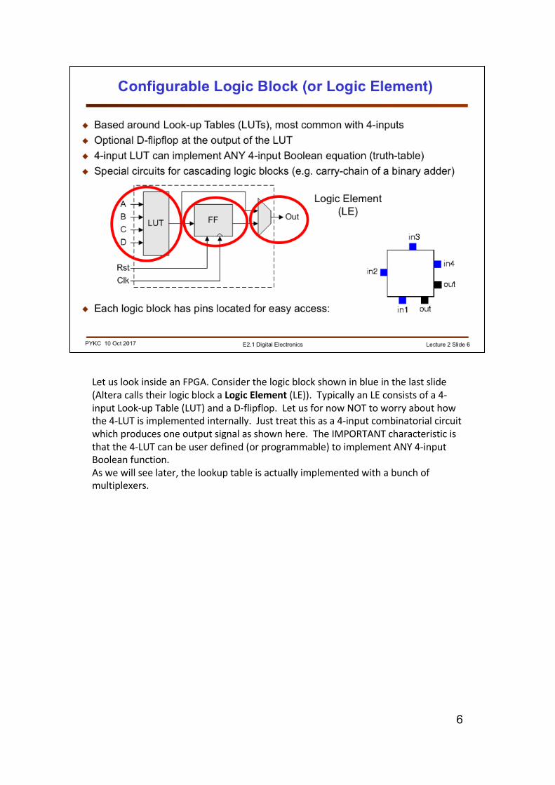
LetuslookinsideanFPGA.Considerthelogicblockshowninblueinthelastslide(AlteracallstheirlogicblockaLogicElement(LE)).TypicallyanLEconsistsofa4-inputLook-upTable(LUT)andaD-flipflop.LetusfornowNOTtoworryabouthowthe4-LUTisimplementedinternally.Justtreatthisasa4-inputcombinatorialcircuitwhichproducesoneoutputsignalasshownhere.TheIMPORTANTcharacteristicisthatthe4-LUTcanbeuserdefined(orprogrammable)toimplementANY4-inputBooleanfunction.Aswewillseelater,thelookuptableisactuallyimplementedwithabunchofmultiplexers.

7
TheLogicElementsaresurroundedbylotsofroutingwiresandinterconnectionswitches.TypicallyasignalwiretotheLogicBlockorLogicElementcanbeconnectedtoanyofthesewiringchannelsthroughaprogrammableconnection(essentiallyadigitalswitch).XilinxFPGAsalsohavededicatedswitchblocksshownhere.Horizontalandverticalwirescanbeconnectedthroughsuchaswitchblockwithprogrammableswitches(fornow,don’tworryhowthat’sdone).
FPGAshavehugeamountoftheseprogrammableresourcesandswitches.Typicallyaverysmallpercentageofthesearebeingconnected(i.e.ON)foragivenapplication.
ThemainadvantageandattractionofFPGAcomesfromtheprogrammableinterconnect– moresothantheprogrammablelogic.
8
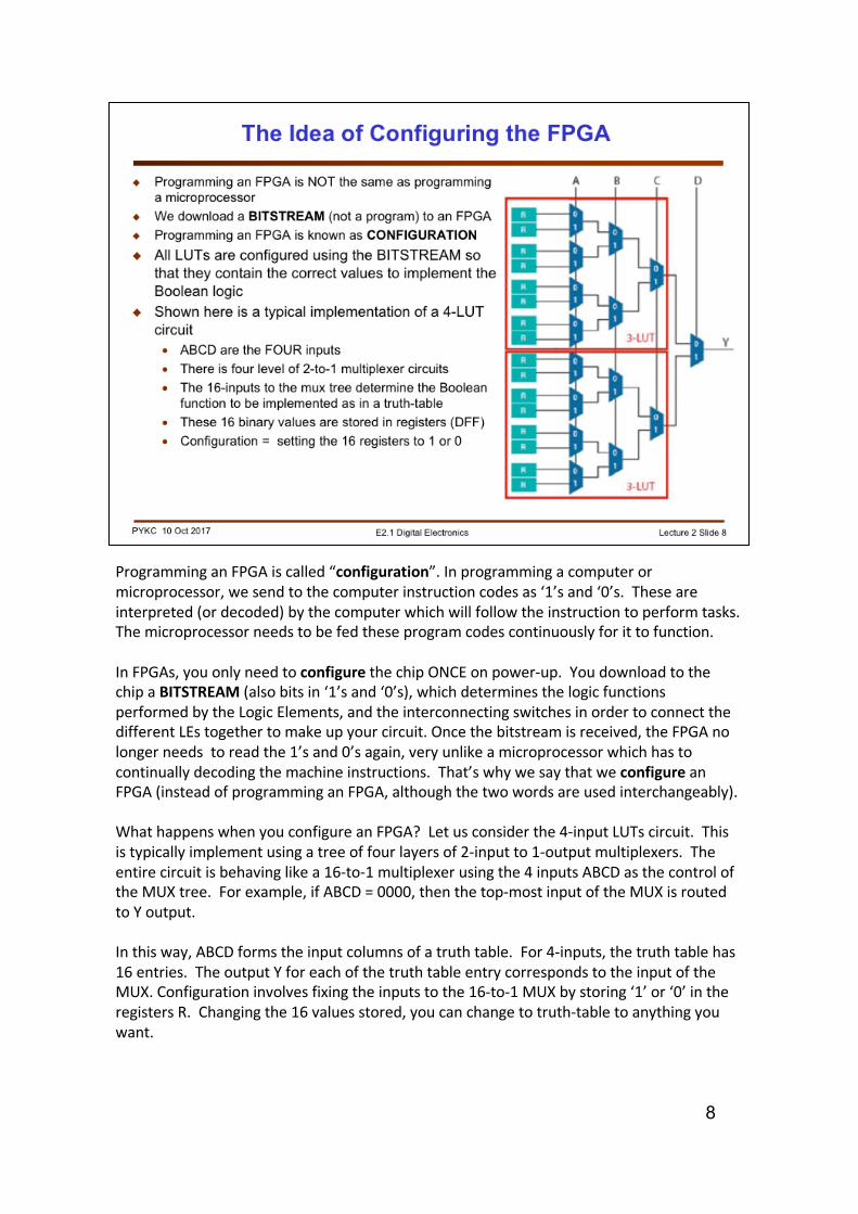
ProgramminganFPGAiscalled“configuration”.Inprogrammingacomputerormicroprocessor,wesendtothecomputerinstructioncodesas‘1’sand‘0’s.Theseareinterpreted(ordecoded)bythecomputerwhichwillfollowtheinstructiontoperformtasks.Themicroprocessorneedstobefedtheseprogramcodescontinuouslyforittofunction.
InFPGAs,youonlyneedtoconfigure thechipONCEonpower-up.YoudownloadtothechipaBITSTREAM (alsobitsin‘1’sand‘0’s),whichdeterminesthelogicfunctionsperformedbytheLogicElements,andtheinterconnectingswitchesinordertoconnectthedifferentLEstogethertomakeupyourcircuit.Oncethebitstream isreceived,theFPGAnolongerneedstoreadthe1’sand0’sagain,veryunlikeamicroprocessorwhichhastocontinuallydecodingthemachineinstructions.That’swhywesaythatweconfigure anFPGA(insteadofprogramminganFPGA,althoughthetwowordsareusedinterchangeably).
WhathappenswhenyouconfigureanFPGA?Letusconsiderthe4-inputLUTscircuit.Thisistypicallyimplementusingatreeoffourlayersof2-inputto1-outputmultiplexers.Theentirecircuitisbehavinglikea16-to-1multiplexerusingthe4inputsABCDasthecontroloftheMUXtree.Forexample,ifABCD=0000,thenthetop-mostinputoftheMUXisroutedtoYoutput.
Inthisway,ABCDformstheinputcolumnsofatruthtable.For4-inputs,thetruthtablehas16entries.TheoutputYforeachofthetruthtableentrycorrespondstotheinputoftheMUX.Configurationinvolvesfixingtheinputstothe16-to-1MUXbystoring‘1’ or‘0’ intheregistersR.Changingthe16valuesstored,youcanchangetotruth-tabletoanythingyouwant.
9
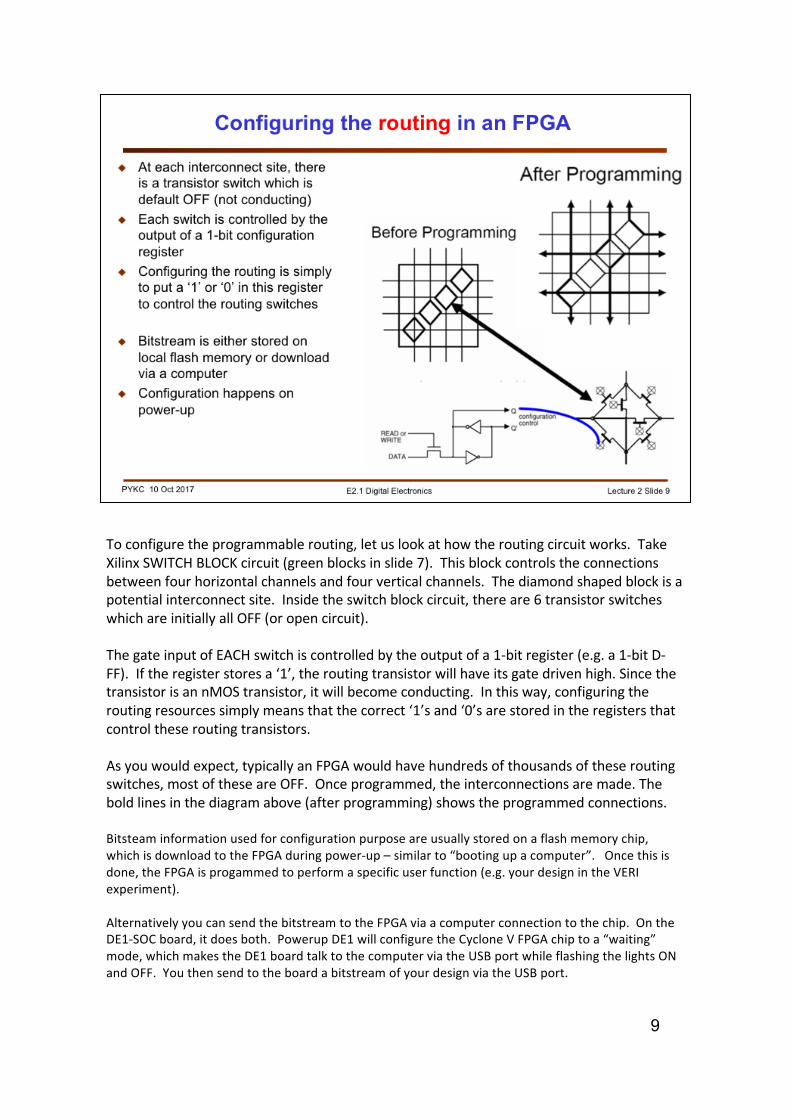
Toconfiguretheprogrammablerouting,letuslookathowtheroutingcircuitworks.TakeXilinxSWITCHBLOCKcircuit(greenblocksinslide7).Thisblockcontrolstheconnectionsbetweenfourhorizontalchannelsandfourverticalchannels.Thediamondshapedblockisapotentialinterconnectsite.Insidetheswitchblockcircuit,thereare6transistorswitcheswhichareinitiallyallOFF(oropencircuit).
ThegateinputofEACHswitchiscontrolledbytheoutputofa1-bitregister(e.g.a1-bitD-FF).Iftheregisterstoresa‘1’,theroutingtransistorwillhaveitsgatedrivenhigh.SincethetransistorisannMOS transistor,itwillbecomeconducting.Inthisway,configuringtheroutingresourcessimplymeansthatthecorrect‘1’sand‘0’sarestoredintheregistersthatcontroltheseroutingtransistors.
Asyouwouldexpect,typicallyanFPGAwouldhavehundredsofthousandsoftheseroutingswitches,mostoftheseareOFF.Onceprogrammed,theinterconnectionsaremade.Theboldlinesinthediagramabove(afterprogramming)showstheprogrammedconnections.
Bitsteam informationusedforconfigurationpurposeareusuallystoredonaflashmemorychip,whichisdownloadtotheFPGAduringpower-up– similarto“bootingupacomputer”.Oncethisisdone,theFPGAisprogammed toperformaspecificuserfunction(e.g.yourdesignintheVERIexperiment).
Alternativelyyoucansendthebitstream totheFPGAviaacomputerconnectiontothechip.OntheDE1-SOCboard,itdoesboth.Powerup DE1willconfiguretheCycloneVFPGAchiptoa“waiting”mode,whichmakestheDE1boardtalktothecomputerviatheUSBportwhileflashingthelightsONandOFF.Youthensendtotheboardabitstream ofyourdesignviatheUSBport.
10
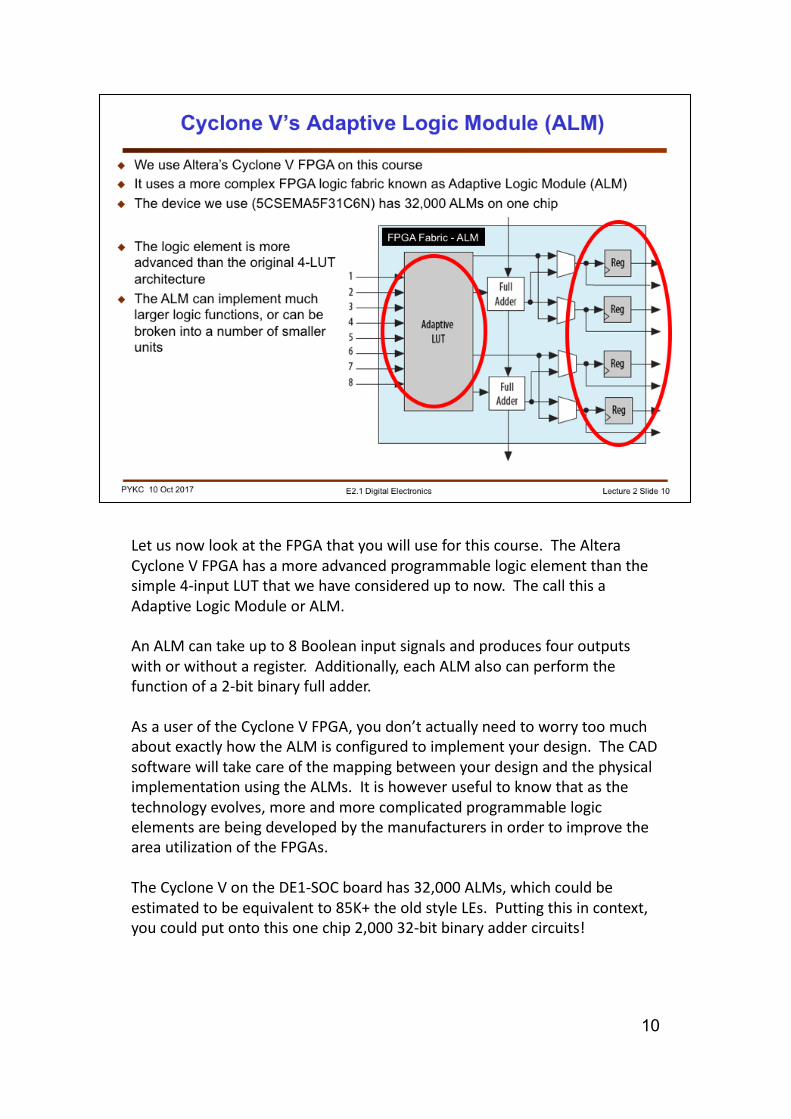
LetusnowlookattheFPGAthatyouwilluseforthiscourse.TheAlteraCycloneVFPGAhasamoreadvancedprogrammablelogicelementthanthesimple4-inputLUTthatwehaveconsidereduptonow.ThecallthisaAdaptiveLogicModuleorALM.
AnALMcantakeupto8Booleaninputsignalsandproducesfouroutputswithorwithoutaregister.Additionally,eachALMalsocanperformthefunctionofa2-bitbinaryfulladder.
AsauseroftheCycloneVFPGA,youdon’tactuallyneedtoworrytoomuchaboutexactlyhowtheALMisconfiguredtoimplementyourdesign.TheCADsoftwarewilltakecareofthemappingbetweenyourdesignandthephysicalimplementationusingtheALMs.Itishoweverusefultoknowthatasthetechnologyevolves,moreandmorecomplicatedprogrammablelogicelementsarebeingdevelopedbythemanufacturersinordertoimprovetheareautilizationoftheFPGAs.
TheCycloneVontheDE1-SOCboardhas32,000ALMs,whichcouldbeestimatedtobeequivalentto85K+theoldstyleLEs.Puttingthisincontext,youcouldputontothisonechip2,00032-bitbinaryaddercircuits!
11
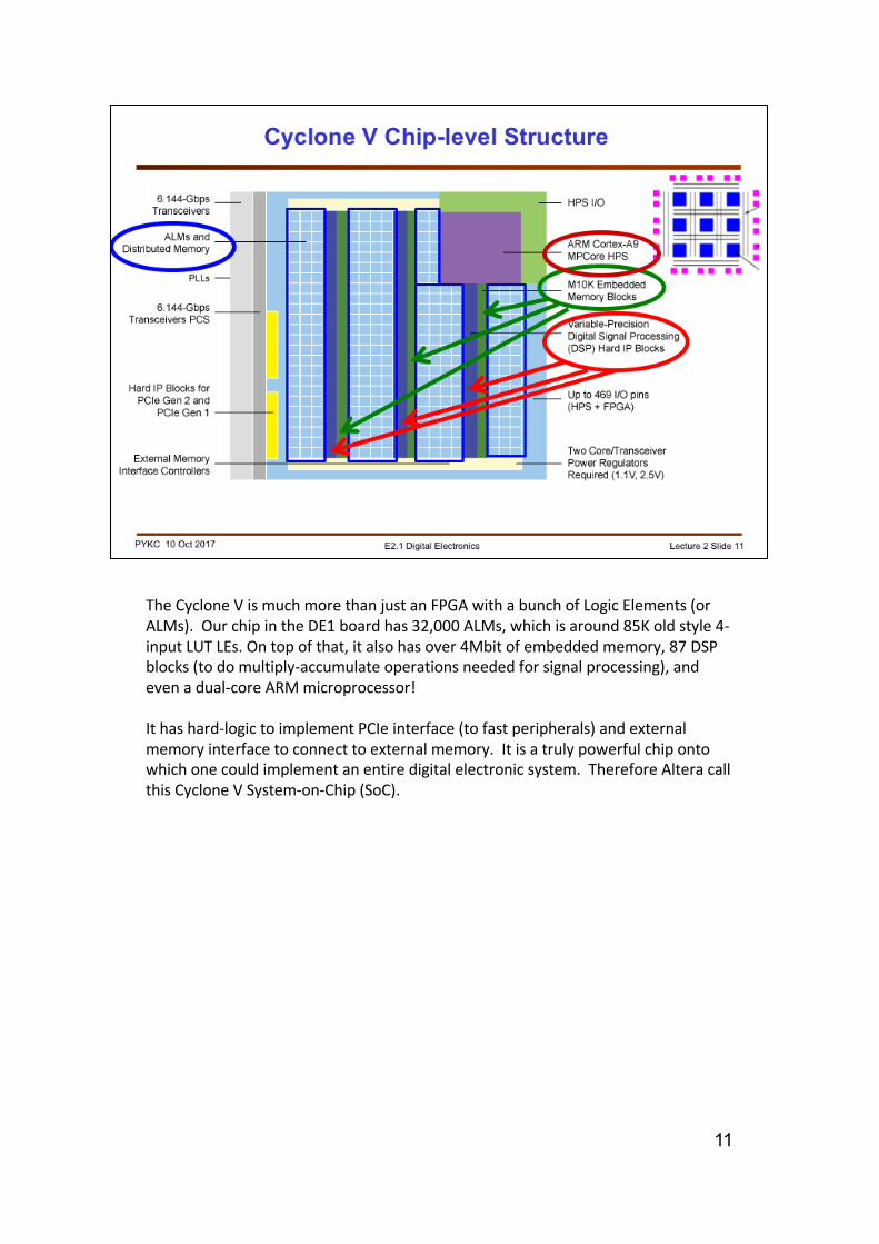
TheCycloneVismuchmorethanjustanFPGAwithabunchofLogicElements(orALMs).OurchipintheDE1boardhas32,000ALMs,whichisaround85Koldstyle4-inputLUTLEs.Ontopofthat,italsohasover4Mbitofembeddedmemory,87DSPblocks(todomultiply-accumulateoperationsneededforsignalprocessing),andevenadual-coreARMmicroprocessor!
Ithashard-logictoimplementPCIe interface(tofastperipherals)andexternalmemoryinterfacetoconnecttoexternalmemory.Itisatrulypowerfulchipontowhichonecouldimplementanentiredigitalelectronicsystem.ThereforeAlteracallthisCycloneVSystem-on-Chip(SoC).
12
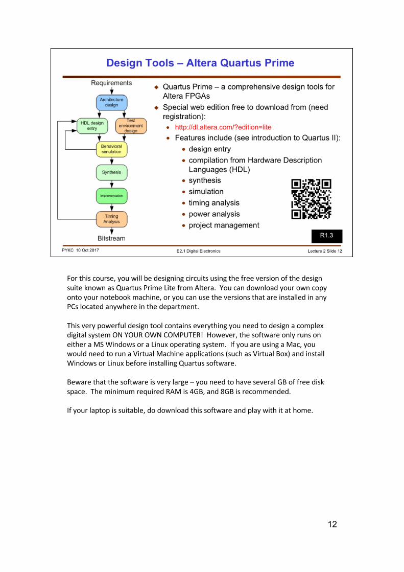
Forthiscourse,youwillbedesigningcircuitsusingthefreeversionofthedesignsuiteknownasQuartus PrimeLitefromAltera.Youcandownloadyourowncopyontoyournotebookmachine,oryoucanusetheversionsthatareinstalledinanyPCslocatedanywhereinthedepartment.
ThisverypowerfuldesigntoolcontainseverythingyouneedtodesignacomplexdigitalsystemONYOUROWNCOMPUTER!However,thesoftwareonlyrunsoneitheraMSWindowsoraLinuxoperatingsystem.IfyouareusingaMac,youwouldneedtorunaVirtualMachineapplications(suchasVirtualBox)andinstallWindowsorLinuxbeforeinstallingQuartus software.
Bewarethatthesoftwareisverylarge– youneedtohaveseveralGBoffreediskspace.TheminimumrequiredRAMis4GB,and8GBisrecommended.
Ifyourlaptopissuitable,dodownloadthissoftwareandplaywithitathome.

13
ThisslideshowsyouthefunctionalblocksoftheDE1-SoCboard.Thishaseverythingyouneedtestbasicdesignsinvolvingswitches,7-segmentdisplaysandevenaVGAoutput.

14
Ialsoprovideapurpose-builtADC/DACboardtosupportthelabexperiment.Thisadd-onboardinonlyneededinweek3onwardsduringthelaboratorysessions.Sofornow,youcanignoreit.