Embed Size (px)
Citation preview
Department of EECS University of California, Berkeley
EECS 105 Fall 2003, Lecture 16
Lecture 16:
Small Signal Amplifiers
Prof. Niknejad
Department of EECS University of California, Berkeley
EECS 105 Fall 2003, Lecture 16 Prof. A. Niknejad
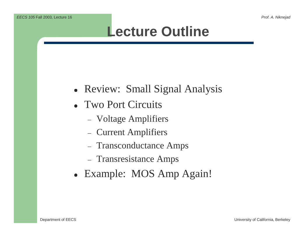
Lecture Outline
Review: Small Signal Analysis
Two Port Circuits– Voltage Amplifiers
– Current Amplifiers
– Transconductance Amps
– Transresistance Amps
Example: MOS Amp Again!
Department of EECS University of California, Berkeley
EECS 105 Fall 2003, Lecture 16 Prof. A. Niknejad
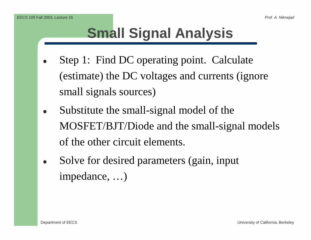
Small Signal Analysis
Step 1: Find DC operating point. Calculate
(estimate) the DC voltages and currents (ignore
small signals sources)
Substitute the small-signal model of the
MOSFET/BJT/Diode and the small-signal models
of the other circuit elements.
Solve for desired parameters (gain, input
impedance, …)

Department of EECS University of California, Berkeley
EECS 105 Fall 2003, Lecture 16 Prof. A. Niknejad
A Simple Circuit: An MOS Amplifier
DSI
GSV
sv
DR DDV
GS GS sv V v= +
ov
Input signal
Output signal
Supply “Rail”
Department of EECS University of California, Berkeley
EECS 105 Fall 2003, Lecture 16 Prof. A. Niknejad
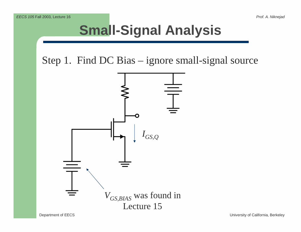
Small-Signal Analysis
Step 1. Find DC Bias – ignore small-signal source
VGS,BIAS was found inLecture 15
IGS,Q
Department of EECS University of California, Berkeley
EECS 105 Fall 2003, Lecture 16 Prof. A. Niknejad
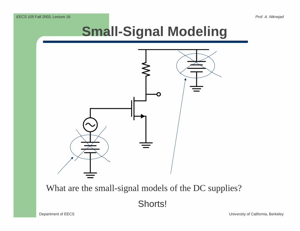
Small-Signal Modeling
What are the small-signal models of the DC supplies?
Shorts!
Department of EECS University of California, Berkeley
EECS 105 Fall 2003, Lecture 16 Prof. A. Niknejad
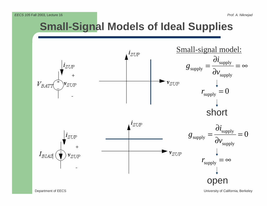
Small-Signal Models of Ideal Supplies
Small-signal model:
supplysupply
supply
ig
v
∂= = ∞
∂
supply 0r =
supplysupply
supply
0i
gv
∂= =
∂
supplyr = ∞
short
open
Department of EECS University of California, Berkeley
EECS 105 Fall 2003, Lecture 16 Prof. A. Niknejad
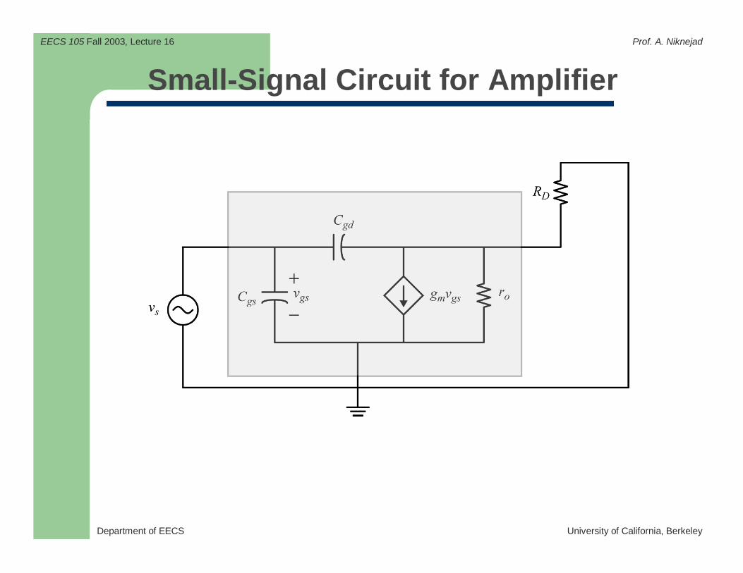
Small-Signal Circuit for Amplifier
Department of EECS University of California, Berkeley
EECS 105 Fall 2003, Lecture 16 Prof. A. Niknejad
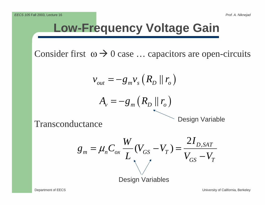
Low-Frequency Voltage Gain
Consider first ω 0 case … capacitors are open-circuits
Transconductance
,2( ) D SAT
m n ox GS TGS T
IWg C V V
L V Vµ= − =
−
( )||out m s D ov g v R r= −
( )||v m D oA g R r= −
Design Variable
Design Variables
Department of EECS University of California, Berkeley
EECS 105 Fall 2003, Lecture 16 Prof. A. Niknejad
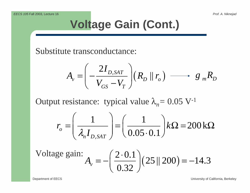
Voltage Gain (Cont.)
Substitute transconductance:
Output resistance: typical value λn= 0.05 V-1
,
1 1200k
0.05 0.1on D SAT
r kIλ
= = Ω = Ω ⋅
Voltage gain: ( )2 0.125 || 200 14.3
0.32vA⋅ = − = −
( ),2||D SAT
v D oGS T
IA R r
V V
= − −
m Dg R
Department of EECS University of California, Berkeley
EECS 105 Fall 2003, Lecture 16 Prof. A. Niknejad
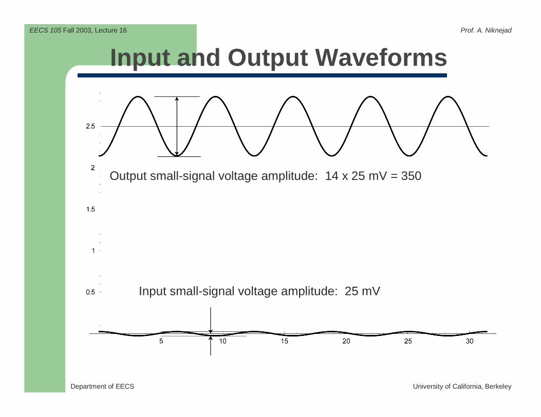
Input and Output Waveforms
Output small-signal voltage amplitude: 14 x 25 mV = 350
Input small-signal voltage amplitude: 25 mV
Department of EECS University of California, Berkeley
EECS 105 Fall 2003, Lecture 16 Prof. A. Niknejad
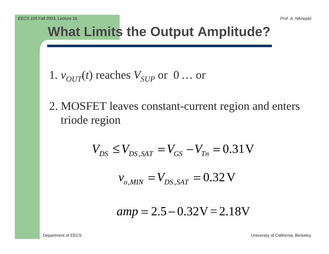
What Limits the Output Amplitude?
1. vOUT(t) reaches VSUP or 0 … or
2. MOSFET leaves constant-current region and enterstriode region
, 0.31VDS DS SAT GS TnV V V V≤ = − =
, , 0.32Vo MIN DS SATv V= =
2.5 0.32V = 2.18Vamp = −
Department of EECS University of California, Berkeley
EECS 105 Fall 2003, Lecture 16 Prof. A. Niknejad
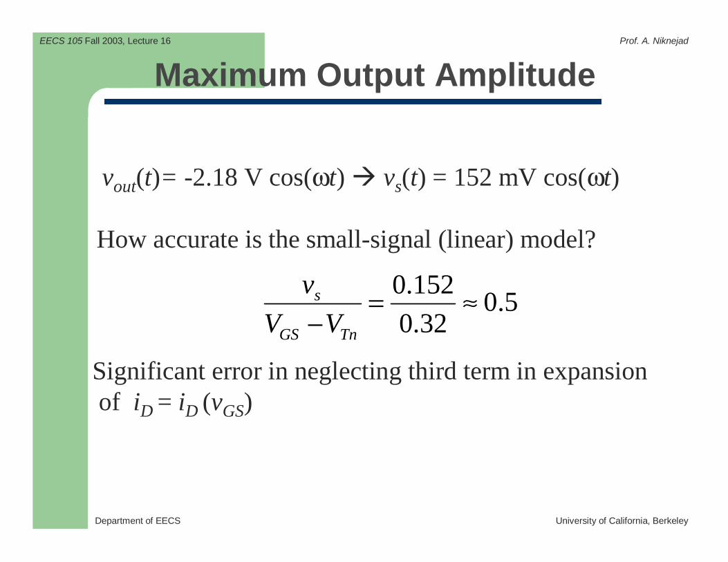
Maximum Output Amplitude
vout(t)= -2.18 V cos(ωt) vs(t) = 152 mV cos(ωt)
How accurate is the small-signal (linear) model?
0.1520.5
0.32s
GS Tn
v
V V= ≈
−
Significant error in neglecting third term in expansionof iD = iD (vGS)
Department of EECS University of California, Berkeley
EECS 105 Fall 2003, Lecture 16 Prof. A. Niknejad
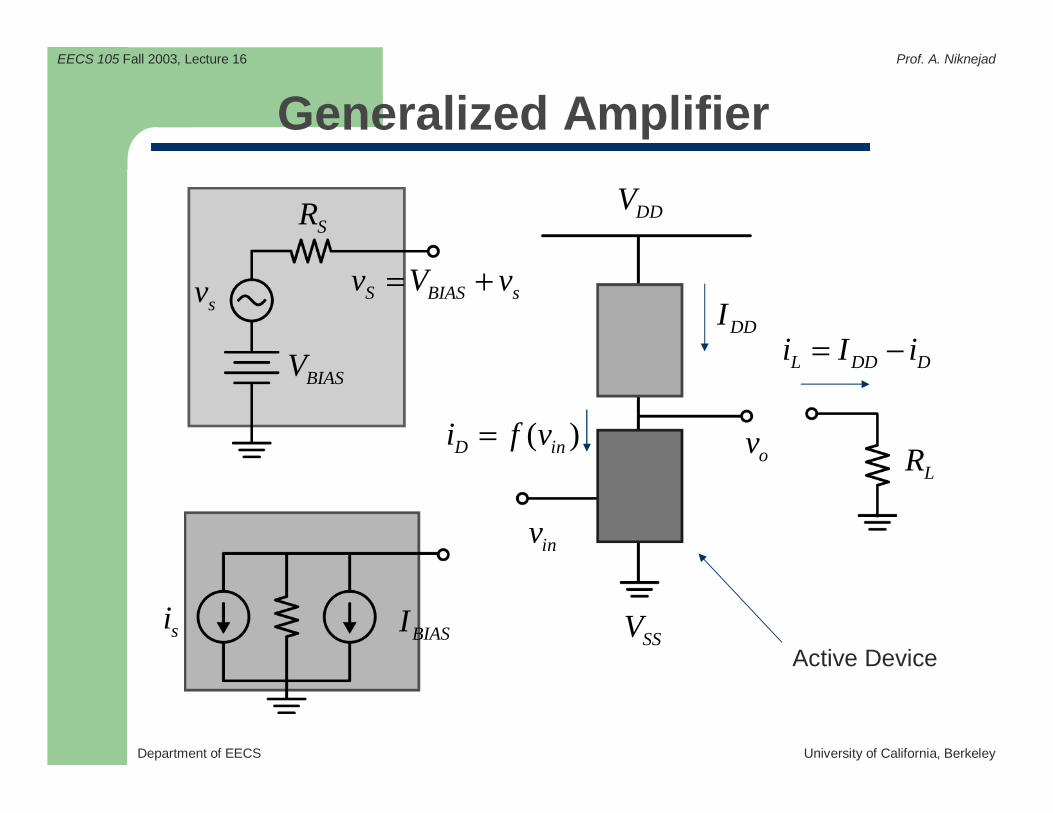
Generalized Amplifier
sv S BIAS sv V v= +
ov
BIASV
DDV
SSVBIASIsi
SR
DDIL DD Di I i= −
( )D ini f v=LR
inv
Active Device

Department of EECS University of California, Berkeley
EECS 105 Fall 2003, Lecture 16 Prof. A. Niknejad
Amplifier Terminology
Sources: Signal, its source resistance, and bias voltage or current
Load: Use resistor in Chap. 8, but could be a general impedance
Port: A pair of terminals across which a voltage and an associated current are defined
Source, Load: “one port”
Amplifier: “two port”
Department of EECS University of California, Berkeley
EECS 105 Fall 2003, Lecture 16 Prof. A. Niknejad
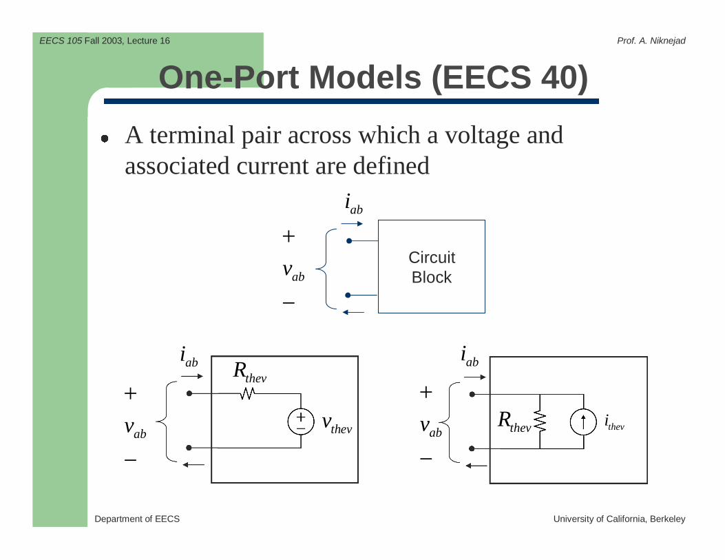
One-Port Models (EECS 40)
A terminal pair across which a voltage and associated current are defined
CircuitBlockabv
+
−
abi
thevv
thevR
abv
+
−
abi
thevithevRabv
+
−
abi
Department of EECS University of California, Berkeley
EECS 105 Fall 2003, Lecture 16 Prof. A. Niknejad
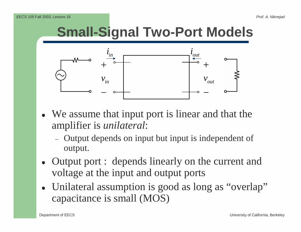
Small-Signal Two-Port Models
We assume that input port is linear and that the amplifier is unilateral: – Output depends on input but input is independent of
output.
Output port : depends linearly on the current and voltage at the input and output ports
Unilateral assumption is good as long as “overlap”capacitance is small (MOS)
inv
+
−outv
+
−
outiini
Department of EECS University of California, Berkeley
EECS 105 Fall 2003, Lecture 16 Prof. A. Niknejad
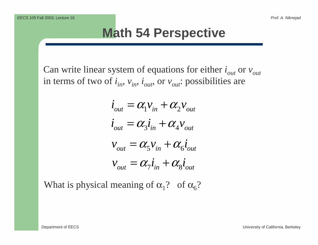
Math 54 Perspective
Can write linear system of equations for either iout or vout
in terms of two of iin, vin, iout, or vout: possibilities are
1 2out in outi v vα α= +
3 4out in outi i vα α= +
5 6out in outv v iα α= +
7 8out in outv i iα α= +
What is physical meaning of α1? of α6?
Department of EECS University of California, Berkeley
EECS 105 Fall 2003, Lecture 16 Prof. A. Niknejad
EE Perspective
Four amplifier types: determined by the output signal and the input signal … both of which we select (usually obvious)– Voltage Amp (VV)
– Current Amp (II)
– Transconductance Amp (VI)
– Transresistance Amp (IV)
We need methods to find the 6 α parameters for the four models and equivalent circuits for unilateral two ports
Department of EECS University of California, Berkeley
EECS 105 Fall 2003, Lecture 16 Prof. A. Niknejad
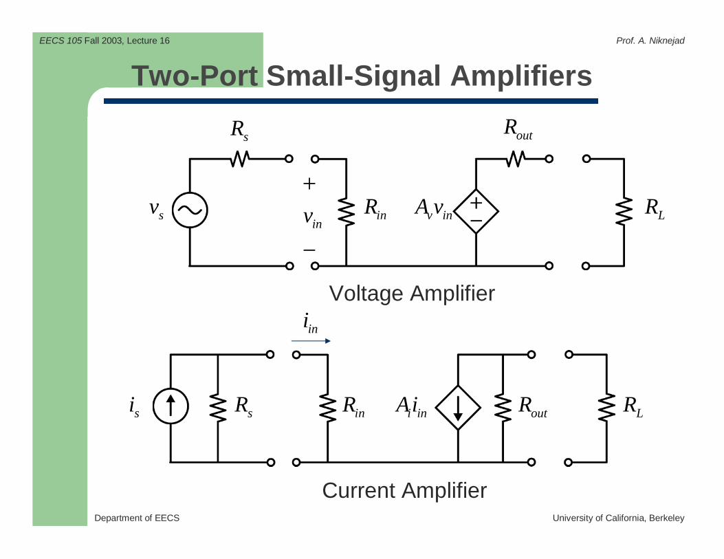
Two-Port Small-Signal Amplifiers
si sR inR outR LRi inAi
ini
sv
sR
inR
outR
LRv inA vinv
+
−
Current Amplifier
Voltage Amplifier
Department of EECS University of California, Berkeley
EECS 105 Fall 2003, Lecture 16 Prof. A. Niknejad
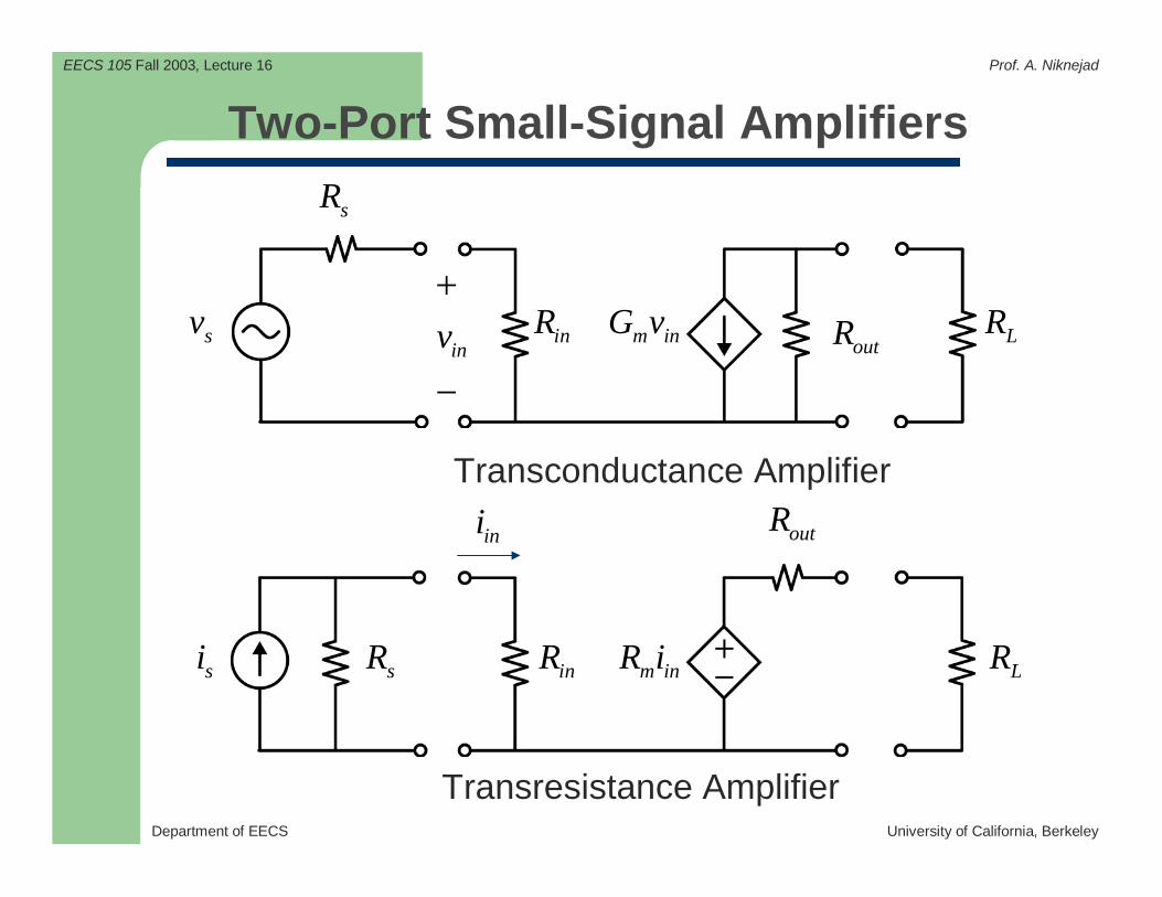
Two-Port Small-Signal Amplifiers
sv
sR
inRoutR LRm inG v
inv
+
−
si sR inR
outR
LRm inR i
ini
Transresistance Amplifier
Transconductance Amplifier
Department of EECS University of California, Berkeley
EECS 105 Fall 2003, Lecture 16 Prof. A. Niknejad
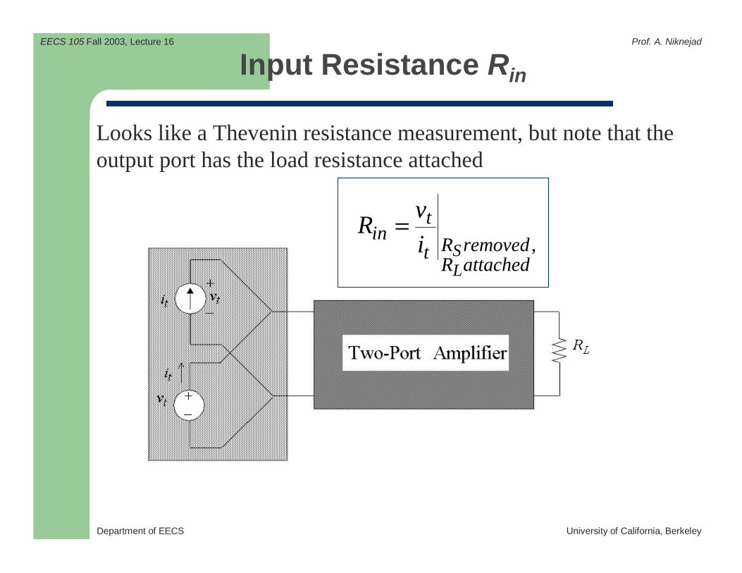
Input Resistance Rin
Looks like a Thevenin resistance measurement, but note that theoutput port has the load resistance attached
attachedRremovedRt
tin
LSi
vR
,=
Department of EECS University of California, Berkeley
EECS 105 Fall 2003, Lecture 16 Prof. A. Niknejad
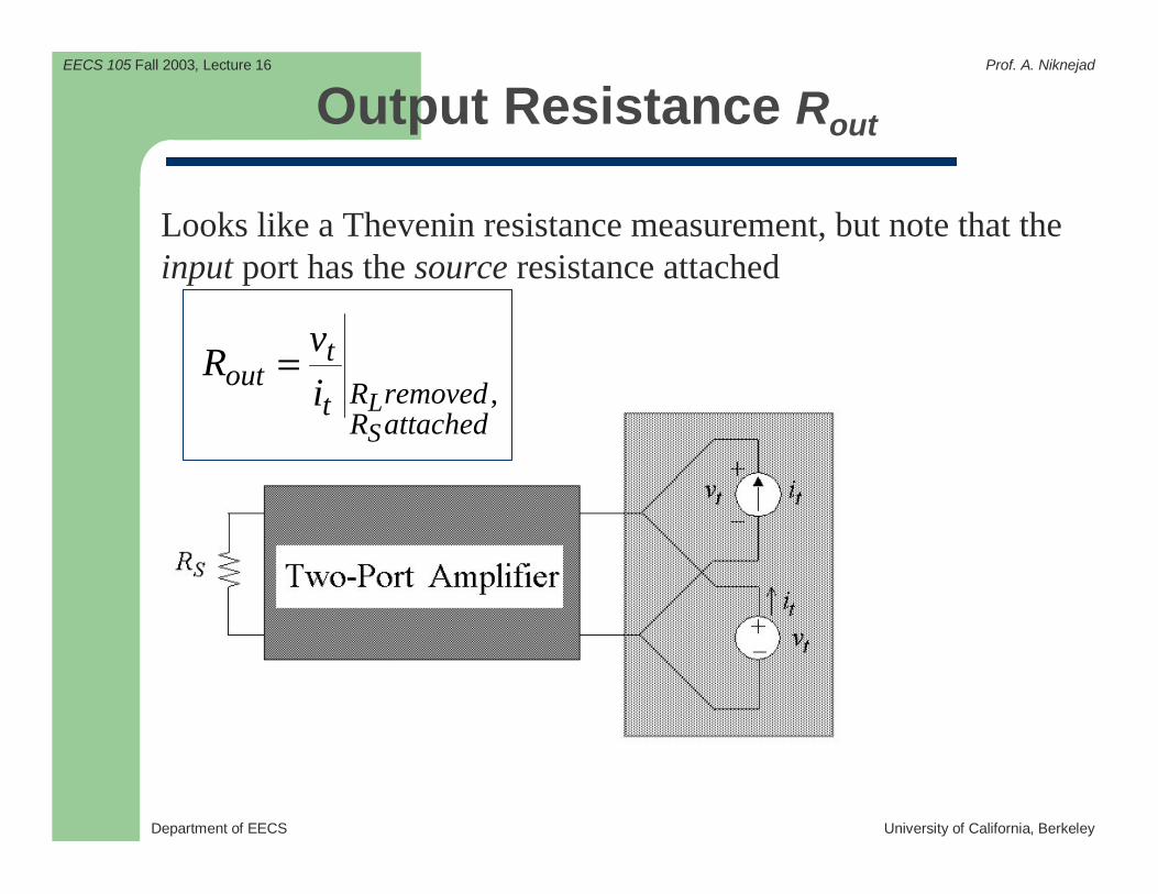
Output Resistance Rout
Looks like a Thevenin resistance measurement, but note that theinput port has the source resistance attached
attachedRremovedRt
tout
SLi
vR
,=

Department of EECS University of California, Berkeley
EECS 105 Fall 2003, Lecture 16 Prof. A. Niknejad
Finding the Voltage Gain Av
Key idea: the output port is open-circuited and the source resistance is shorted
Department of EECS University of California, Berkeley
EECS 105 Fall 2003, Lecture 16 Prof. A. Niknejad
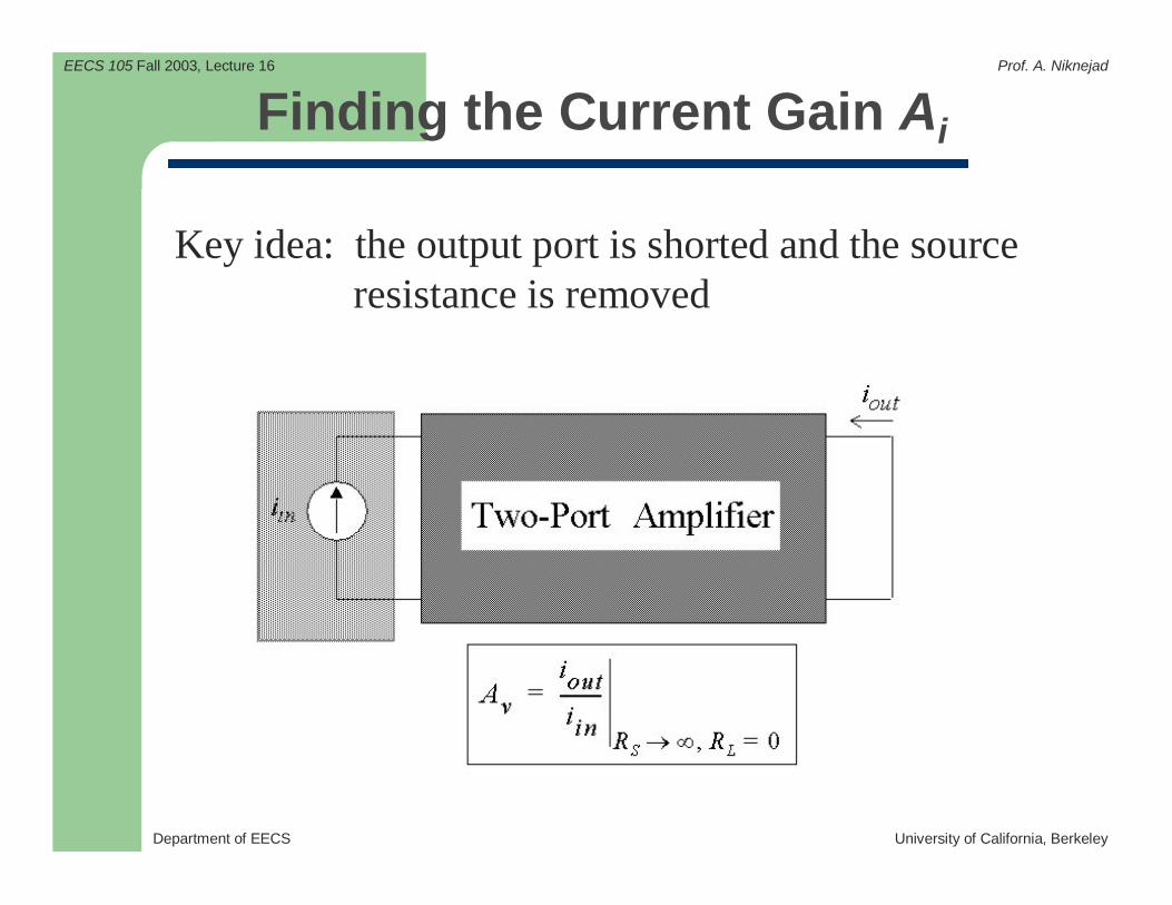
Finding the Current Gain Ai
Key idea: the output port is shorted and the sourceresistance is removed
Department of EECS University of California, Berkeley
EECS 105 Fall 2003, Lecture 16 Prof. A. Niknejad
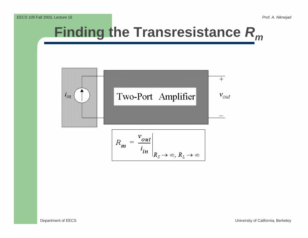
Finding the Transresistance Rm
Department of EECS University of California, Berkeley
EECS 105 Fall 2003, Lecture 16 Prof. A. Niknejad
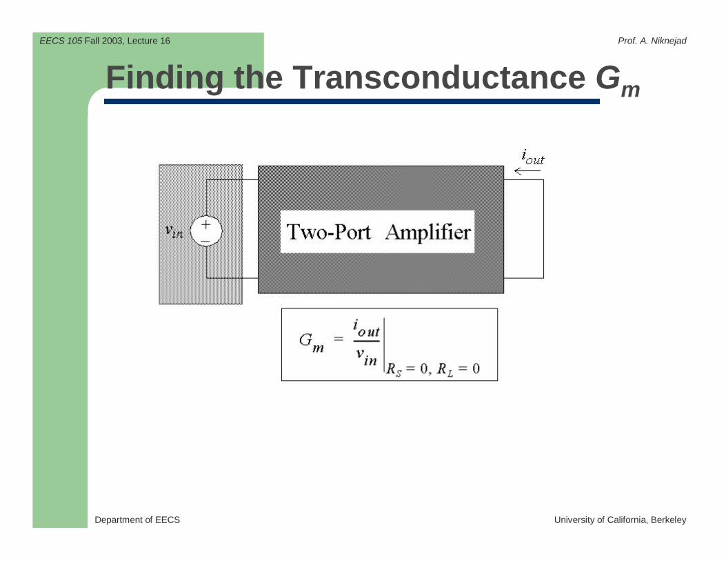
Finding the Transconductance Gm
Department of EECS University of California, Berkeley
EECS 105 Fall 2003, Lecture 16 Prof. A. Niknejad
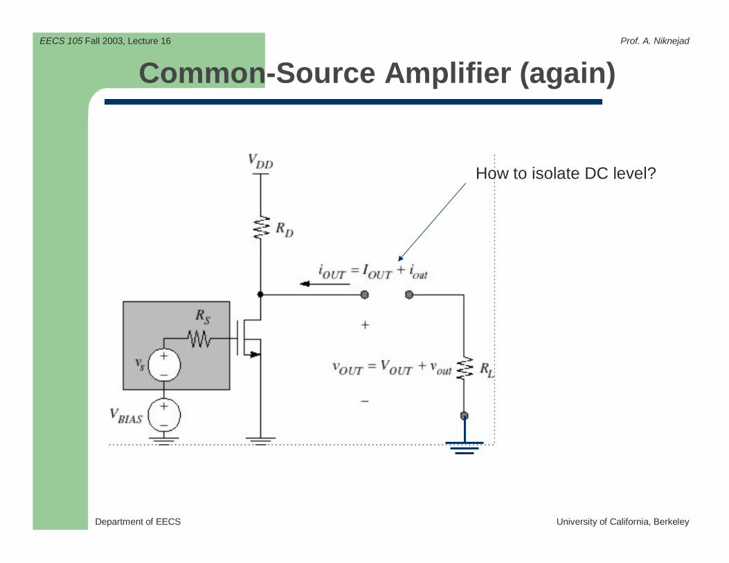
Common-Source Amplifier (again)
How to isolate DC level?
Department of EECS University of California, Berkeley
EECS 105 Fall 2003, Lecture 16 Prof. A. Niknejad
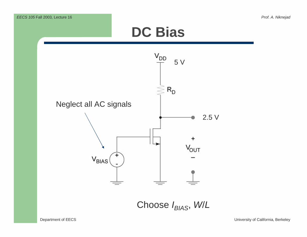
DC Bias
Neglect all AC signals
5 V
2.5 V
Choose IBIAS, W/L
Department of EECS University of California, Berkeley
EECS 105 Fall 2003, Lecture 16 Prof. A. Niknejad
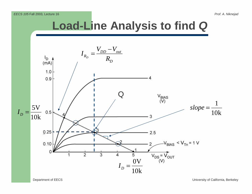
Load-Line Analysis to find Q
Q
D
DD outR
D
V VI
R
−=
1
10kslope =
0V
10kDI =
5V
10kDI =

Department of EECS University of California, Berkeley
EECS 105 Fall 2003, Lecture 16 Prof. A. Niknejad
Small-Signal Analysis
inR = ∞
Department of EECS University of California, Berkeley
EECS 105 Fall 2003, Lecture 16 Prof. A. Niknejad
sv
sR
inRoutR LRm inG v
inv
+
−
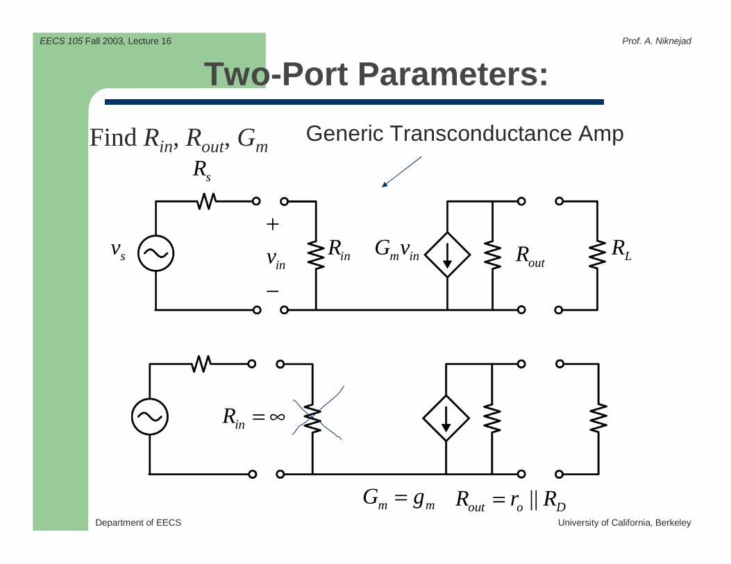
Two-Port Parameters:
Find Rin, Rout, Gm
inR = ∞
m mG g= ||out o DR r R=
Generic Transconductance Amp
Department of EECS University of California, Berkeley
EECS 105 Fall 2003, Lecture 16 Prof. A. Niknejad
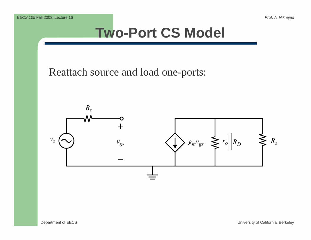
Two-Port CS Model
Reattach source and load one-ports: