Embed Size (px)
Citation preview

Lecture 16. Molecular Self-Assembly
We have discussed examples of molecular devices, including molecular rectifiers, wires and
switches. These devices use molecules as active elements, but the basic architectures are not
drastically different from the conventional microelectronic devices. For example, the use of
metal electrodes or wires to connect the molecules to the external world and the control of the
current with a back gate are similar to what have been used in the conventional devices. It is not
clear how these approaches can be scaled down to the molecular scale and how to integrate
millions of tiny molecules into a device. Self-assembly is one of the few practical strategies that
may overcome the above difficulties. We have briefly mentioned two examples of self-assembly:
self-assembled monolayers of thiols and L-B films. Here we will provide an overview of self-
assembly together with an example on how it can be used to fabricate an electronic device.
Self-assembly
The word, "self-assembly", has been widely used (or perhaps, overused) in recent literatures.
Processes ranging from the non-covalent association of organic molecules in solution to the
growth of semiconductor quantum dots on solid substrates are referred to as self-assembly.
Following the definition by Whiteside,1 self-assembly is the autonomous organization of
components into patterns or structures without human intervention. The term is limited to
processes that involve pre-existing components (separate or distinct parts of a disordered
structure), are reversible, and can be controlled by proper design of the components. "Self-
assembly" is thus not synonymous with "formation."
Types of Self-Assembly
Self-assembling processes are common throughout nature and technology. They involve
components from the molecular (crystals) to the planetary (weather systems) scale and many
different kinds of interactions. The concept of self-assembly is used increasingly in many
disciplines, with a different flavor and emphasis in each.

There are two main kinds of self-assembly: static and dynamic. Static self-assembly (S)
(Table 1; Fig. 1) involves systems that are at global or local equilibrium and do not dissipate
energy. For example, molecular crystals2, 3 are formed by static self-assembly; so are most
folded, globular proteins. In static self-assembly, formation of the ordered structure may require
energy (for example in the form of stirring), but once it is formed, it is stable. Most research in
self-assembly has focused on this static type.
Figure 1. Examples of static self-assembly. (A) Crystal structure of a ribosome. (B) Self-assembled peptide-amphiphile nanofibers. (C) An array of millimeter-sized polymeric plates assembled at a water/perfluorodecalin interface by capillary interactions. (D) Thin film of a nematic liquid crystal on an isotropic substrate. (E) Micrometer-sized metallic polyhedra folded

from planar substrates. (F) A three-dimensional aggregate of micrometer plates assembled by capillary forces. [Image credits: (A) from (24); (B) from (25); (C) from (26); (D) from (27); (E) from (28); (F) from (29)]
In dynamic self-assembly (D) (Table 1; Fig. 2), the interactions responsible for the formation of structures or patterns between components only occur if the system is dissipating
energy. The patterns formed by competition between reaction and diffusion in oscillating chemical reactions are simple examples; biological cells are much more complex ones. The study of dynamic self-assembly is in its infancy.
Figure 2. Examples of dynamic self-assembly. (A) An optical micrograph of a cell with fluorescently labeled cytoskeleton and nucleus; microtubules (~24 nm in diameter) are colored red. (B) Reaction-diffusion waves in a Belousov-Zabatinski reaction in a 3.5-inch Petri dish. (C) A simple aggregate of three millimeter-sized, rotating, magnetized disks interacting with one

another via vortex-vortex interactions. (D) A school of fish. (E) Concentric rings formed by charged metallic beads 1 mm in diameter rolling in circular paths on a dielectric support. (F) Convection cells formed above a micropatterned metallic support. The distance between the centers of the cells is ~2 mm.
Table 1. Examples of self-assembly (S, static, D, dynamic, T, templated, B, biological).
System Type Applications/importance
Atomic, ionic, and molecular crystals S Materials, electronic and optoelectronicsPhase-separated and ionic layered
polymers S
Self-assembled monolayers (SAMs) S, T Microfabrication, sensors, nanoelectronics
Lipid bilayers and black lipid films S Biomembranes, emulsions Liquid crystals S Displays
Colloidal crystals S Band gap materials, molecular sieves Bubble rafts S Models of crack propagation
Macro- and mesoscopic structures (MESA)
S or D, T Electronic circuits
Fluidic self-assembly S, T Microfabrication "Light matter" D, T
Oscillating and reaction-diffusion reactions D Biological oscillations
Bacterial colonies D, B
Swarms (ants) and schools (fish) D, B New models for computation/optimization
Weather patterns D Solar systems D
Galaxies D
Two further variants of self-assembly are also identified. In templated self-assembly (T), interactions between the components and regular features in their environment determine the structures that form. Crystallization on surfaces that determine the morphology of the crystal is one example; crystallization of colloids in three-dimensional optical fields is another. The characteristic of biological self-assembly (B) is the variety and complexity of the functions that it produces.

Common Features of Self-Assembly Self-assembly reflects information coded in individual components. The information includes
geometry (shape), nature of their mutual interactions and interactions with environment, and
mass. Geometry plays important roles in the final assembled structure, the kinetics of self-
assembly process as well as the interactions. The interactions are determined by also the surface
properties, charge, polarizability, magnetic dipole, mass of the components. Mass affects the
gravitational force but also the dynamics of self-assembly. The design of components that
organize themselves into desired patterns and functions is the key to applications of self-
assembly.
The components must be able to move with respect to one another. Their steady-state positions
balance attractions and repulsions. Molecular self-assembly involves noncovalent or weak
covalent interactions (van der Waals, electrostatic, and hydrophobic interactions, hydrogen and
coordination bonds). In the self-assembly of larger components--meso- or macroscopic objects--
interactions can often be selected and tailored, and can include interactions such as gravitational
attraction, external electromagnetic fields, and magnetic, capillary, and entropic interactions,
which are not important in the case of molecules.
Because self-assembly requires that the components be mobile, it usually takes place in fluid
phases or on smooth surfaces. The environment can modify the interactions between the
components; the use of boundaries and other templates in self-assembly is particularly important,
because templates can reduce defects and control structures.
Equilibration is usually required to reach ordered structures. If components stick together
irreversibly when they collide, they form a glass rather than a crystal or other regular structure.
Self-assembly requires that the components either equilibrate between aggregated and non-
aggregated states, or adjust their positions relative to one another once in an aggregate.
Self-Assembly in Designed Systems – A example Whiteside’s group demonstrated a self-assembled 3-D microelectronic system. 4 The components
are millimeter-scale polyhedra, with surfaces patterned with solder dots, wires, and light-emitting
diodes. The patterns of dots and wires controlled the structure of the networks formed, which

allowed them to generate electrically functional, three-dimensional networks with both parallel
and serial connections.
The basic unit in the assemblies is a polyhedron, a truncated octahedron (TO), on whose
faces electrical circuits are printed. The circuits include LEDs to demonstrate electrical
connectivity and trace the networks. More complex devices, such as processors, can be included
in the future, at least in principle. The LEDs are wired to patterns of solder dots on adjacent faces
of the polyhedron. The TOs are suspended in an approximately isodense liquid at a temperature
above the melting point of the solder (m.p. ~ 47°C), and allowed to tumble gently into contact
with one another. The drops of molten solder fuse, and the minimization of their interfacial free
energy generates the forces that assemble the TOs into regular structures. 5Processes based on
capillary interactions between solder drops have been used previously to assemble electronic and
mechanical structures: examples include "flip-chip" technology6 and the rotation of parts of
microstructures into nonplanar orientations7. During assembly, recognition of the pattern of dots
on one face by that on another orients and registers the patterns, and generates dot-on-dot
electrical connections among polyhedra. Self-assembly of polyhedra can generate networks in
which the LEDs are connected either in parallel or in series. Figure 3 outlines both the fabrication
of the patterned polyhedra and their self-assembly into 3D structures that include electrical
networks.

They used a scheme in which LEDs were mounted on the hexagonal faces of the TO, and the
solder dots were placed on the square faces. To maximize the rate of self-assembly, all of the
square faces of the TO had the same fourfold symmetric pattern of solder dots. With this pattern,
correct registration of patterns on juxtaposed faces occurred in one of four indistinguishable ways;
dots on the patterns that transformed into each other under fourfold rotational symmetry were
equivalent and served the same function. On the 3 mm by 3 mm square face, the width of all of
the solder dots was ~1 mm (Fig. 4). A common size was required: the solder wetted the copper
with a well-defined contact angle, and each drop of the same size therefore had the same height.
Empirical testing suggested that the optimum distance between adjacent solder dots was
approximately one-half their width. Smaller separations resulted in electrical shorting between
dots due to bridging with solder; larger separations resulted in misalignment. They designed the
Fig. 3. The procedure used to form electrical networks in 3D by self-assembly (12). (A) An array of the basic pattern of copper dots, contact pads, and wires was defined on a flexible copper-polyimide sheet using photolithography and etching. (B) These pattern elements were cut out along the dotted line, (C) glued on the faces of the polyhedron, and (D) LEDs were soldered manually onto the contact pads. (E) The copper dots and wires on the TOs were coated with solder, and self-assembly occurred in hot, isodense, aqueous KBr solution.

shapes of solder dots to give an energy diagram for self-assembly having one large (global)
minimum and relatively small local minima.
The wires that connect different solder dots electrically on each TO were fabricated in the same
way as the dots. When the patterned TOs were dipped in solder, these wires were also covered
with a solder layer. By making the wires substantially narrower (~150 µm) than the diameter of
the dots (~1 mm), they limited the height of the solder film on the wires to ~15% that of the dots.
When the faces self-assembled, the larger dots fused into connections, but the smaller wires did
not touch and fuse (Fig. 4C). It was, as a result, unnecessary to insulate the wires to prevent
shorting, even when they crossed on juxtaposed faces of two TOs.
In current 2D IC technology, pins on processors belong to one of three groups: bus lines (driving
voltage, clock), inputs, and outputs. Bus lines connect processors in parallel; outputs of one
processor connect serially to inputs of adjacent processors.
Fig. 4. Strategies used to design patterns of solder dots. (A) The widths of all the dots in the patterns used were approximately the same. The width of the wires was smaller. (B) A cross-sectional view [section XX' in (A)] of two assembling faces. (C) When the faces connect, the solder dots fuse with each other, whereas the wires between them do not touch. (D) A pattern comprising dots that can be used for both parallel and serial networks.

In the pattern of solder dots (Fig. 4D), the five dots that lie on reflection axes comprise two sets
of dots differentiated by symmetry: {1} and {2, 5, 8, and 11}. During self-assembly, dots from
one set on a TO connect to dots from the same set on another TO. These dots are used for parallel
or bus-line connections. The other dots, {3, 6, 9, and 12} and {4, 7, 10, and 13}, form two
distinct sets related by reflection symmetry. Upon assembly, dots from one set on a TO (e.g.,
outputs from one processor) connect to those from the other set on another TO (e.g., inputs to a
second processor). These dots are used for serial, input/output connections.
Figure 5 shows the realization of a 3D network with parallel connectivity, using self-assembly.
The pattern of solder dots consisted of dots {2, 5, 8, and 11} and {1} (Fig. 4D), which were on
the axes of symmetry of the square face. In the assembled aggregate, LEDs on one TO connected
to those on the adjacent TO in parallel, along three orthogonal directions. The fidelity of the
interconnections was visualized by lighting up the LEDs connected in parallel in the assembly.
This self-assembled, 3D parallel network mimicked bus lines in circuits in which a number of
electrical components are powered by the same common wires.

Figure 5. A self-assembled 2 × 2 × 3 aggregate containing 12 TOs and demonstrating parallel connectivity. (A) The pattern of copper dots, wires, and contact pads used. (B) A patterned TO with three LEDs, prior to assembly. (C) A photograph of the self-assembled aggregate and a penny (to indicate size). Two electrically isolated pairs of wires connected to a battery illuminate six LEDs in an electrically continuous loop involving three TOs. (D) Circuit diagram showing the parallel network formed. The gray circles represent individual TOs. The blue half-circles represent solder dots that connect on juxtaposed faces of two TOs. The LEDs are shown in black. The network contains 16 pairs of wires, which consist of four (red), six (green), and six (blue) pairs in each of the three dimensions. The six LEDs that illuminate are highlighted by black squares

Fig. 6. A self-assembled 2 × 2 × 3 aggregate containing 12 TOs and demonstrating serial connectivity. (A) The pattern of solder dots used. (B) The terminals of a single LED are directly soldered across two contact pads, and a wire is soldered in a way that connects the third contact pad to one of the terminals of the LED, using a polarity in which the anode of the LED connects to dots from the set {3 and 9} and the cathode connects to dots from the set {7 and 13}. (C) A patterned TO prior to assembly. (D) A self-assembled aggregate. The LEDs on different TOs connect to each other in serial loops. The loops were traced by powering pairs of leads. Individual loops range in size from those containing two LEDs to one that contains 10 LEDs; this loop is shown illuminated. (E) The circuit diagram sketching the largest serial loop formed; 10 LEDs illuminate when the loop is connected to a battery (D). The LEDs connect cathode to anode in all loops.
For the realization of a 3D network with serial connectivity (Fig. 5), they used the sets of
solder dots {3, 6, 9, and 12} and {4, 7, 10, and 13} (Fig. 2D) that were off the axes of symmetry
of the square face (14). The important feature of the assembled 3D network was that the cathode
of one LED always connected to the anode of another LED across the assembling faces. The
serial networks were traced by illuminating sets of LEDs (e.g., Fig. 6D).
The 3D assemblies can be designed to be porous: this porosity may allow for cooling fluid to be
pumped through the assemblies. The shape and the distribution of solder dots on the assembling
faces raises interesting questions regarding the design of patterns that best enable the
"recognition" of one pattern by another. Other concepts adapted from 2D self-assembly, such as
hierarchical self-assembly and shape-selective self-assembly, offer more sophisticated strategies
for the fabrication of asymmetrical networks incorporating more than one repeating unit.
It is possible to extend these ideas to more complex networks involving different combinations of
parallel and serial connections. The LEDs in the demonstrations by Whiteside’s group are simple
bipolar electronic devices; to fabricate 3D computational devices, one must incorporate elements
of digital logic. Self-assembly facilitates the formation of highly interconnected elements in both
deterministic and probabilistic networks; it may be possible to use this kind of self-assembly to
generate other logical structures (e.g., artificial neural networks). To extend this approach to a
larger number of elements, and to smaller elements, it will be necessary to develop practical
methods for fabricating these elements; the need for 3D microfabrication permeates 3D self-
assembly, but new methods are beginning to emerge. Although large arrays may have defects, it
may be possible to develop computational algorithms even in defective networks .
References
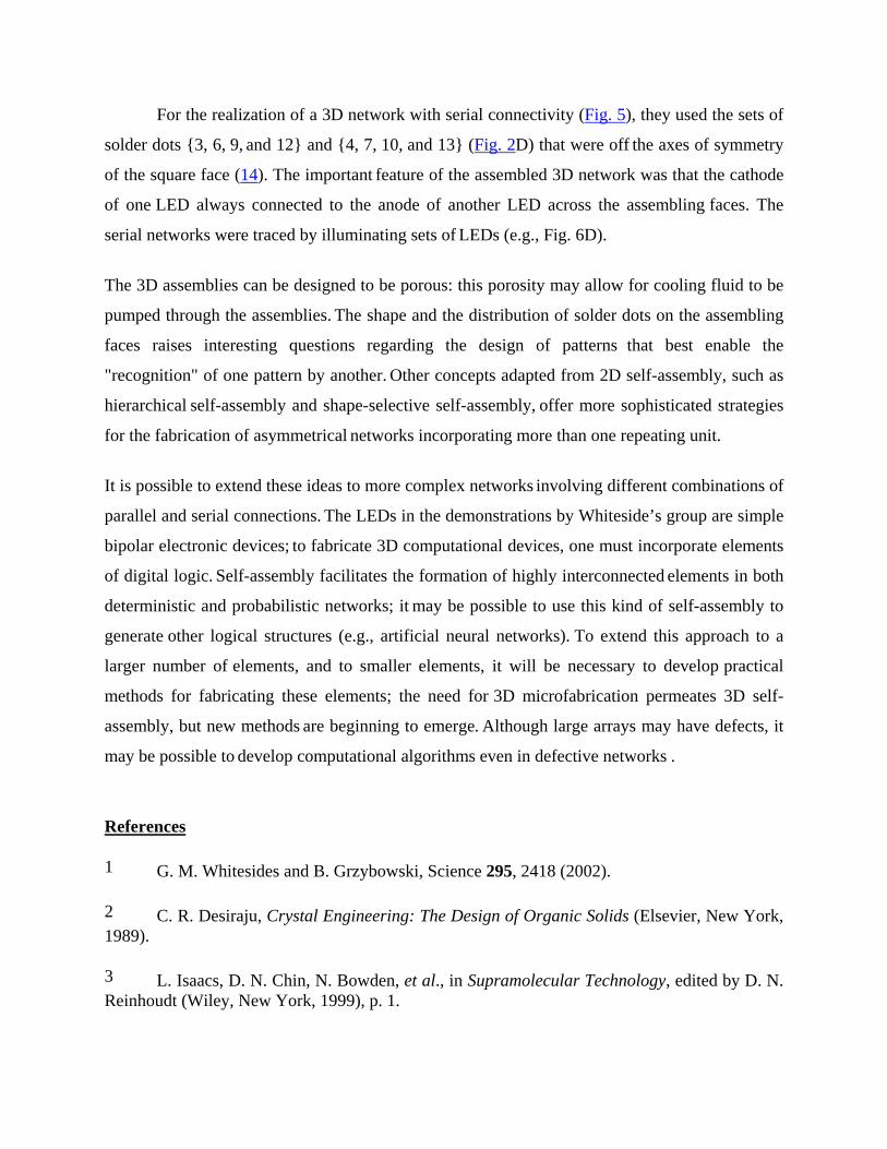
1 G. M. Whitesides and B. Grzybowski, Science 295, 2418 (2002).
2 C. R. Desiraju, Crystal Engineering: The Design of Organic Solids (Elsevier, New York, 1989).
3 L. Isaacs, D. N. Chin, N. Bowden, et al., in Supramolecular Technology, edited by D. N. Reinhoudt (Wiley, New York, 1999), p. 1.

4 D. Gracias, J. Tien, T. L. Breen, et al., Science 289, 1170 (2000).
5 T. L. Breen, J. Tien, S. R. J. Olivier, et al., Science 284, 948 (1999).
6 L. F. Miller, IBM J. Res. Dev. 13, 239 (1969).
7 R. R. A. Syms and E. M. Yeatman, Electron. Lett. 29, 662 (1993).