Embed Size (px)
Citation preview

ECE418 / ECE518 – Spring 2021
Lecture 12 – Wednesday April 21st 2021
1/44
ECE 418 / 518 – Semiconductor Processing
Spring 2021 - John Labram
Lecture 12: OxidationChapter 3 Jaeger
2/44
ECE 418 / 518 – Semiconductor Processing
Spring 2021 - John Labram
Last Time
Si
SiO2SiO2
Pre-Deposition
Dopant gas
Si
Drive-in
Si
SiO2SiO2
• Before the break we covered the basics of diffusion.
1
2

ECE418 / ECE518 – Spring 2021
Lecture 12 – Wednesday April 21st 2021
3/44
ECE 418 / 518 – Semiconductor Processing
Spring 2021 - John Labram
Useful LinksThis subject is widely taught, and online notes are available from
many sources. Here are some good examples:
• http://www-
inst.eecs.berkeley.edu/~ee143/fa10/lectures/Lec_06.pdf
UC Berkeley Notes:
• https://engineering.ucsb.edu/~sumita/courses/Courses/ME14
1B/ME141B_lecture_4_F10.pdf
UC Santa Barbara Notes:
4/44
ECE 418 / 518 – Semiconductor Processing
Spring 2021 - John Labram
Lecture 11• Oxide Properties.
• Oxidation Process.
• Oxide Growth Model.
• Factors Influencing Oxidation Rate.
3
4

ECE418 / ECE518 – Spring 2021
Lecture 12 – Wednesday April 21st 2021
5/44
ECE 418 / 518 – Semiconductor Processing
Spring 2021 - John Labram
Oxide Properties
6/44
ECE 418 / 518 – Semiconductor Processing
Spring 2021 - John Labram
Oxidation• Reasons that SiO2 so widespread in VLSI:
• Forms directly from the Si substrate upon exposure to oxygen containing species (O2 or H2O):
• SiO2 is a high quality electrical insulator (low interface trap density):
Si S + O2(G) → SiO2(S)
Si S + 2H2O L → SiO2 S + 2H2(G)
“Dry”
“Wet”
• Thin (10-50 Å) gate oxide for MOS gate.
• Thick (1000-2000 Å) field oxide for transistor isolation and barrier to dopant diffusion.
5
6

ECE418 / ECE518 – Spring 2021
Lecture 12 – Wednesday April 21st 2021
7/44
ECE 418 / 518 – Semiconductor Processing
Spring 2021 - John Labram
Other Compounds• This is one of the main advantages of Si, and is the main
reason why it is the commercial standard for semiconductors.
Germanium GaAs
Hu et. al. “Native Oxidation Growth on Ge(111) and (100) Surfaces” Small
1(4) (2005) 429.
Thomas et. al. “High electron mobility thin-film transistors based on Ga2O3
grown by atmospheric ultrasonic spray pyrolysis at low temperatures” APL
105 (2014) 092105.
8/44
ECE 418 / 518 – Semiconductor Processing
Spring 2021 - John Labram
Structure of SiO2• Each Si surrounded tetrahedrally by 4 O atoms
• Density of SiO2 < crystalline SiO2.
• Quartz = 2.65 gm/cm3.
• Thermally grown oxide = 2.20 gm/cm3.
• Silicon = 2.33 gm/cm3.
• Open, amorphous structure.
jcrystal.com/
Si
OSi
O
O
OSi
O
OSiSi
OSi
O
O
OSi
O
OSi
OSi
O
OSi
O
OSi
O
OSi
O
OSi
O
OSi
O
OSi
O
OSi
O
1.6 A
2.27 A
7
8

ECE418 / ECE518 – Spring 2021
Lecture 12 – Wednesday April 21st 2021
9/44
ECE 418 / 518 – Semiconductor Processing
Spring 2021 - John Labram
Properties of SiO2• Excellent electrical insulator.
• Resistivity > 1015 Ωcm.
• Band gap ~ 8 eV.
• Crucial in devices.
Al Al
SiO2
Si++
S D
Dielectric
Gate
e- e- e- e- e- e- e- e- e- e- e- e-
+VD
+VG
10/44
ECE 418 / 518 – Semiconductor Processing
Spring 2021 - John Labram
Properties of SiO2• High breakdown electric field strength.
• >10 MV/cm.
Al Al
SiO2
Si++
S D
Dielectric
Gate
e- e- e- e- e- e- e- e- e- e- e- e-
+VD
+VG
9
10

ECE418 / ECE518 – Spring 2021
Lecture 12 – Wednesday April 21st 2021
11/44
ECE 418 / 518 – Semiconductor Processing
Spring 2021 - John Labram
Properties of SiO2• Stable:
• Conformal oxide growth on exposed Si surface.
Si Si
SiO2
• Good diffusion mask for common dopants:
𝐷𝑆𝑖𝑂2 ≪ 𝐷𝑆𝑖
Si
SiO2SiO2
• Down to 10-9 Torr, T > 900°C.
12/44
ECE 418 / 518 – Semiconductor Processing
Spring 2021 - John Labram
Properties of SiO2• Excellent etch selectivity between Si and SiO2.
Si
SiO2
Si
HF Dip
11
12

ECE418 / ECE518 – Spring 2021
Lecture 12 – Wednesday April 21st 2021
13/44
ECE 418 / 518 – Semiconductor Processing
Spring 2021 - John Labram
Oxidation: Applications• Oxide grown by oxidation is used at two important steps in
chip manufacture.
• Field oxide.
• Gate oxide.
• Field oxide:
• Field oxide isolates different transistors on a chip.
Source DrainSource DrainP-WellN-Well
Gate Gate
Transistor 1 Transistor 2
Fieldoxide
14/44
ECE 418 / 518 – Semiconductor Processing
Spring 2021 - John Labram
Oxidation: Applications• Gate oxide
• Recall that the gate on a transistor works because the charge effects the holes and electrons across the oxide
P-Si
Insulator
N-Si
Source DrainGate
N-Si
Gate oxide
• Currently the gate oxide is only 10 - 50 Å thick. (A sheet of paper is 1,000,000 Å thick!)
13
14
ECE418 / ECE518 – Spring 2021
Lecture 12 – Wednesday April 21st 2021
15/44
ECE 418 / 518 – Semiconductor Processing
Spring 2021 - John Labram
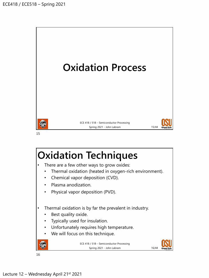
Oxidation Process
16/44
ECE 418 / 518 – Semiconductor Processing
Spring 2021 - John Labram
Oxidation Techniques
• Thermal oxidation (heated in oxygen-rich environment).
• Chemical vapor deposition (CVD).
• Plasma anodization.
• Physical vapor deposition (PVD).
• Thermal oxidation is by far the prevalent in industry.
• We will focus on this technique.
• Best quality oxide.
• Unfortunately requires high temperature.
• Typically used for insulation.
• There are a few other ways to grow oxides:
15
16

ECE418 / ECE518 – Spring 2021
Lecture 12 – Wednesday April 21st 2021
17/44
ECE 418 / 518 – Semiconductor Processing
Spring 2021 - John Labram
Thermal Oxidation• Two approaches:
• Dry Oxidation (O2):
• Uses oxygen gas:
• High quality.
• Slow oxidation rate.
• Small maximum thickness (i.e. gate oxide).
• Wet Oxidation (H2O):
• Diffusion speed is higher.
• Lower quality.
• Uses water vapor:
• Faster oxidation rate.
Si S + O2(G) → SiO2(S)
Si S + 2H2O Vapor → SiO2 S + 2H2(G)
18/44
ECE 418 / 518 – Semiconductor Processing
Spring 2021 - John Labram
Oxidation: Mechanism• The oxygen containing species must diffuse through the oxide
layer to the unreacted silicon.
• This makes for a “cleaner” process.
Silicon substrate
Water vapor
OXIDEOxygen species
diffuses through
oxide Water vapor
Silicon dioxide
Silicon
Surface hydroxyl
17
18

ECE418 / ECE518 – Spring 2021
Lecture 12 – Wednesday April 21st 2021
19/44
ECE 418 / 518 – Semiconductor Processing
Spring 2021 - John Labram
Oxidation: Mechanism• Oxygen reacts with silicon to form silicon dioxide:
Si S + O2(G) → SiO2(S)
Si S + 2H2O Vapor → SiO2 S + 2H2(G)
Si
SiO2
Si
Time
• We can work out the thickness of Si consumed from the number density.
Original
Thickness
𝑋0
𝑋𝑆𝑖
𝑋𝑆𝑖 = 𝑋0𝑛𝑜𝑥𝑛𝑆𝑖
# density of SiO2
# density of Si
𝑋𝑆𝑖 = 𝑋02.3 × 10²²
5 × 1022= 0.46𝑋0
20/44
ECE 418 / 518 – Semiconductor Processing
Spring 2021 - John Labram
Oxide Growth Model
19
20

ECE418 / ECE518 – Spring 2021
Lecture 12 – Wednesday April 21st 2021
21/44
ECE 418 / 518 – Semiconductor Processing
Spring 2021 - John Labram
Deal & Grove Model
• It’s no accident that the world leader in Si chip technology, Intel, has been led by Andy Grove.
• As a young researcher at Fairchild Semiconductor, he “wrote the book” on SiO2
growth: the Deal-Grove model.
• Without easy growth of SiO2
on Si, there would be no semiconductor industry.
1997
22/44
ECE 418 / 518 – Semiconductor Processing
Spring 2021 - John Labram
Deal & Grove Model• We will talk about dry growth (O2), but principles are the same
for H2O.
Si
SiO2
O2
Si
• SiO2 growth occurs at the Si/SiO2 interface because:
𝐷O2 SiO2 ≫ 𝐷Si SiO2
I.e. diffusion coefficient of O2 in SiO2 is much higher than the
diffusion coefficient of Si in SiO2.
• For this class we will carry out only parts of the derivation, and use the results. It closely follows the textbook.
• A more in-depth derivation can be found in ECE611.
• We want to quantify the growth rate of the oxide.
21
22

ECE418 / ECE518 – Spring 2021
Lecture 12 – Wednesday April 21st 2021
23/44
ECE 418 / 518 – Semiconductor Processing
Spring 2021 - John Labram
Modelling Oxidation• The oxidation process is best visualized by this picture:
Si
SiO2
SiOriginal
Thickness
𝑋0
𝑋𝑆𝑖
• In order for oxidation to occur, oxygen must reach the silicon interface.
• As the oxide grows, the oxygen must pass through more SiO2, and the growth rate will slow.
• The figure on the right is one way to visualize the process.
SiO2 Si
𝑋0𝑥
𝑁
24/44
ECE 418 / 518 – Semiconductor Processing
Spring 2021 - John Labram
Oxidation Diagram• The labels are as follows:
• 𝑁 is the concentration of O2 (# / volume).
• 𝑥 is the distance from the surface of the oxide.
• 𝑋0 is the distance of the interface between the Si and SiO2 from the surface (will change with time).
• 𝑁𝑖 is the concentration of O2 at the interface between the Si and SiO2.
• 𝐽 is the oxygen flux (# / area / time).
• We will assume the flux is the same at every position up to 𝑋0.
SiO2 Si
𝑋0
𝑁𝑖
𝑥
𝑁
𝐽
𝑁0
23
24

ECE418 / ECE518 – Spring 2021
Lecture 12 – Wednesday April 21st 2021
25/44
ECE 418 / 518 – Semiconductor Processing
Spring 2021 - John Labram
Modelling Oxidation• We can describe the flux (𝐽) using Fick’s First Law:
𝐽 = −𝐷𝜕𝑁 𝑥, 𝑡
𝜕𝑥
• Where 𝐷 is the diffusion coefficient of O2 in SiO2.
• The negative sign means that particles tend to move from regions of high concentration to regions of low concentration.
• For our derivation we are going to make the approximation that oxygen flux is constant everywhere and that 𝑁 ∝ 𝑥.
• In this case we can just approximate Fick’s First Law as:
𝐽 = −𝐷𝑁𝑖 − 𝑁0𝑋0 − 0
SiO2 Si
𝑋0
𝑁𝑖
𝑥
𝑁
𝐽
𝑁0
= −𝐷𝑁𝑖 − 𝑁0𝑋0
(3.3)
(3.4)
26/44
ECE 418 / 518 – Semiconductor Processing
Spring 2021 - John Labram
Oxidation Reaction
• At the interface between the SiO2 and Si we assume the oxidation rate (𝑘𝑠) is proportional to the concentration of O2 at the interface (𝑁𝑖):
𝐽 = −𝐷𝑁𝑖 − 𝑁0𝑋0
SiO2 Si
𝑋0
𝑁𝑖
𝑥
𝑁
𝐽
𝑁0
𝐽 = 𝑘𝑠𝑁𝑖
• We quantify the conversion of silicon and oxygen into + O2 to SiO2 via a chemical reaction rate: 𝑘𝑠 . This has units of length / time, (e.g. cm/s).
• Equating 𝑁𝑖’s in these two equations:
𝐽 =𝐷𝑁0
𝑋0 + Τ𝐷 𝑘𝑠I.e. the flux is
limited/defined by the reaction rate
(3.4)
(3.5)
(3.6)
25
26

ECE418 / ECE518 – Spring 2021
Lecture 12 – Wednesday April 21st 2021
27/44
ECE 418 / 518 – Semiconductor Processing
Spring 2021 - John Labram
Oxide Growth Rate• So, by balancing diffusion with reaction rate we can describe
the O2 flux as:
𝐽 =𝐷𝑁0
𝑋0 + Τ𝐷 𝑘𝑠
• Recall, our goal is to determine the rate of oxide growth:
𝑑𝑋0𝑑𝑡
• We define the number of oxygen molecules incorporated into a unit volume of the resulting oxide as 𝑀.
• 𝑀 is a number density and has dimensions of #/[length]3.
• We can hence infer through dimensional analysis:
𝑑𝑋0𝑑𝑡
=𝐽
𝑀=
𝐷𝑁0𝑀 𝑋0 + Τ𝐷 𝑘𝑠
(3.6)
(3.7)
28/44
ECE 418 / 518 – Semiconductor Processing
Spring 2021 - John Labram
Oxide Growth Rate
• We identify this a first order ordinary differential equation.
𝑑𝑋0𝑑𝑡
=𝐷𝑁0
𝑀 𝑋0 + Τ𝐷 𝑘𝑠
• We are not going to solve it, we will just take the solution:
𝑋0 𝑡 = 0.5𝐴 1 +4𝐵
𝐴2𝑡 + 𝜏
Τ1 2
− 1
(3.7)
(3.9)
• Where:
𝐴 =2𝐷
𝑘𝑠𝐵 =
2𝐷𝑁0𝑀
• And 𝜏 is the time it would have taken to grow the initial oxide.
• Bare silicon is very reactive, and in air you will always find your wafer has some native oxide (even if it is only ~10Å).
• You can think of 𝜏 as the time before 𝑡 = 0 required to grow this native oxide.
27
28

ECE418 / ECE518 – Spring 2021
Lecture 12 – Wednesday April 21st 2021
29/44
ECE 418 / 518 – Semiconductor Processing
Spring 2021 - John Labram
Oxide Thickness𝑋0 𝑡 = 0.5𝐴 1 +
4𝐵
𝐴2𝑡 + 𝜏
Τ1 2
− 1 (3.9)
• Growth parameters are often quoted with this notation:
• This is the equation that tells us how thick our oxide would be for a certain oxidation time (𝑡) and certain parameters (𝐴, 𝐵, 𝜏).
• Be aware of the non-standard units for length and time.
30/44
ECE 418 / 518 – Semiconductor Processing
Spring 2021 - John Labram
Growth Regimes𝑋0 𝑡 = 0.5𝐴 1 +
4𝐵
𝐴2𝑡 + 𝜏
Τ1 2
− 1 (3.9)
• It turns out we can simplify this equation for different times.
• We define Short Times as 𝑡 + 𝜏 ≪ Τ𝐴2 4𝐵:
𝑋0 𝑡 =𝐵
𝐴𝑡 + 𝜏 (3.10)
• We define Long Times as 𝑡 + 𝜏 ≫ Τ𝐴2 4𝐵, 𝑡 ≫ 𝜏:
𝑋0 𝑡 = 𝐵𝑡 (3.11)
• For this reason, sometimes Τ𝐴 𝐵 is the called the Linear Coefficient and 𝐵 is called the Parabolic Coefficient.
29
30

ECE418 / ECE518 – Spring 2021
Lecture 12 – Wednesday April 21st 2021
31/44
ECE 418 / 518 – Semiconductor Processing
Spring 2021 - John Labram
Growth Regimes• If we plotted the oxide thickness (𝑋0) as a function of growth
time, we would hence expect to observe something like this:
Parabolic
𝑋0 ∝ 𝑡
𝑡
𝑋0
𝑋0 ∝ 𝑡
Linear
𝑡 ≈𝐴2
4𝐵− 𝜏
32/44
ECE 418 / 518 – Semiconductor Processing
Spring 2021 - John Labram
Factors Influencing
Oxidation Rate
31
32

ECE418 / ECE518 – Spring 2021
Lecture 12 – Wednesday April 21st 2021
33/44
ECE 418 / 518 – Semiconductor Processing
Spring 2021 - John Labram
Diffusion Coefficient• As we talked about in the last lecture, diffusion is a
temperature-activated process:
𝐷 = 𝐷0 exp−𝐸𝐴𝑘𝐵𝑇
(3.12)
• Where:
• 𝐷 is the diffusion coefficient (of oxygen in SiO2).
• 𝐷0 is the diffusion pre-factor.
• 𝐸𝐴 is the activation energy.
• 𝑘𝐵 is the Boltzmann Constant.
• 𝑇 is the Temperature.
34/44
ECE 418 / 518 – Semiconductor Processing
Spring 2021 - John Labram
Diffusion Coefficient
• Dry oxide:
• 700-1,200 °C.
• 1 atm (101325 Pa).
• Typical = 100nm/hr.
• SiO2 Density is higher.
• Used for gate oxide.
• Wet oxide:
• 750-1,100 °C.
• 25 atm (2.5 × 10⁶ Pa).
• Typical = 1μm/hr.
• SiO2 Density is lower, more porus.
• Used for field oxide and etch oxide.
33
34
ECE418 / ECE518 – Spring 2021
Lecture 12 – Wednesday April 21st 2021
35/44
ECE 418 / 518 – Semiconductor Processing
Spring 2021 - John Labram
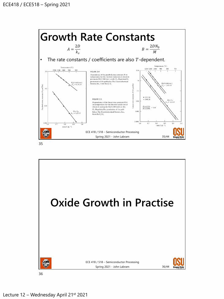
Growth Rate Constants
• The rate constants / coefficients are also 𝑇-dependent.
𝐴 =2𝐷
𝑘𝑠𝐵 =
2𝐷𝑁0𝑀
36/44
ECE 418 / 518 – Semiconductor Processing
Spring 2021 - John Labram
Oxide Growth in Practise
35
36

ECE418 / ECE518 – Spring 2021
Lecture 12 – Wednesday April 21st 2021
37/44
ECE 418 / 518 – Semiconductor Processing
Spring 2021 - John Labram
First Substrates are Cleaned• RCA Clean (Lecture 2)
• Organic strip.
• Piranha Solution.
• Native oxide removal.
• HF.
• Heavy metal removal.
• HCl:H2O2:H2O.
• Dump rinse.
• 18 MΩcm DI H2O.
• Spin Dry.
38/44
ECE 418 / 518 – Semiconductor Processing
Spring 2021 - John Labram
Initial Oxidation Regime• Experimentally, this is observed:
How do we explain this?
37
38

ECE418 / ECE518 – Spring 2021
Lecture 12 – Wednesday April 21st 2021
39/44
ECE 418 / 518 – Semiconductor Processing
Spring 2021 - John Labram
Initial Oxidation Regime• Many models have been proposed.
• It is likely the O2:SiO2 interface is not abrupt:
O2 SiO2 Si
𝑥
O2 Conc.
40/44
ECE 418 / 518 – Semiconductor Processing
Spring 2021 - John Labram
Dopants• Common dopants in Si enhance oxidation at higher
concentration
Boron
Oxide thickness vs. wet oxidation time at 640 mTorr for three different boron concentrations (Sze)
Phosphorus
Data for dry oxidation at 1 atm and 900˚C
Linear, B/A, and parabolic, B, rate
constants vs. phosphorus concentration.
39
40
ECE418 / ECE518 – Spring 2021
Lecture 12 – Wednesday April 21st 2021
41/44
ECE 418 / 518 – Semiconductor Processing
Spring 2021 - John Labram
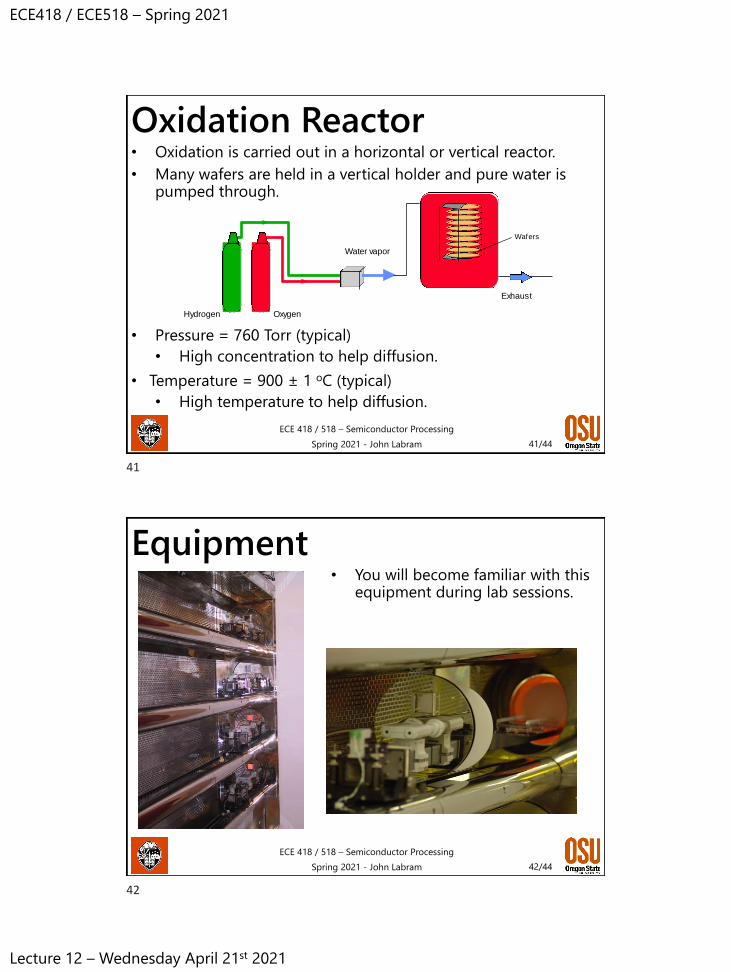
Oxidation Reactor• Oxidation is carried out in a horizontal or vertical reactor.
• Many wafers are held in a vertical holder and pure water is pumped through.
Wafers
Hydrogen
Water vapor
Oxygen
Exhaust
• Pressure = 760 Torr (typical)
• High concentration to help diffusion.
• Temperature = 900 ± 1 oC (typical)
• High temperature to help diffusion.
42/44
ECE 418 / 518 – Semiconductor Processing
Spring 2021 - John Labram
Equipment• You will become familiar with this
equipment during lab sessions.
41
42

ECE418 / ECE518 – Spring 2021
Lecture 12 – Wednesday April 21st 2021
43/44
ECE 418 / 518 – Semiconductor Processing
Spring 2021 - John Labram
Summary• We will have covered the
growth of silicon oxide.
Wafers
Hydrogen
Water vapor
Oxygen
Exhaust
SiO2 Si
𝑋0
𝑁𝑖
𝑥
𝑁
𝐽
𝑁0
44/44
ECE 418 / 518 – Semiconductor Processing
Spring 2021 - John Labram
Next Time…• Next time will start to cover
transistors.
S D
𝐿
𝑊
𝐿
𝑊
𝐷
DS
Gate
Dielectric
Semiconductor
Substrate
𝐼𝐷
𝑉𝐷
𝑉𝐺
43
44


![Chapter 12 Alcohols from Carbonyl Compounds: Oxidation ... · Alcohols from Carbonyl Compounds: Oxidation-Reduction ... for reduction is [H] Chapter 12 5 Oxidation: ... cannot form](https://img.dokumen.tips/doc/110x75/5ac7c7027f8b9a5d718c0ec2/chapter-12-alcohols-from-carbonyl-compounds-oxidation-from-carbonyl-compounds.jpg)