Embed Size (px)
Citation preview

10511 SY/63010 SY 20100621-S00013/20310 SY 20100128-S00002 / D1609 SY / 70908 SY IM / 41608 SY IM No.A1066-1/21
LE25FU406B Overview
The LE25FU406B is a serial interface-compatible flash memory device with a 512K × 8-bit configuration. It uses a single 2.5V power supply for both reading and writing (program and erase functions) and does not require a special power supply. As such, it can support on-board programming. It has three erase functions, each of which corresponds to the size of the memory area in which the data is to be erased at one time: the small sector (4K bytes) erase function, the sector (64K bytes) erase function, and the chip erase function (for erasing all the data together). The memory space can be efficiently utilized by selecting one of these functions depending on the application. A page program method is supported for data writing. The page program method of the LE25FU406B can program any amount of data from 1 to 256 bytes. The program time of 2.0ms (typ.) when programming 256 bytes (1 page) at one time makes for fast data writing. While making the most of the features inherent to a serial flash memory device, the LE25FU406B is housed in an 8-pin ultra-miniature package. Serial flash memory devices tend to be at a disadvantage in terms of their read speed, but the LE25FU406B has maximally eliminated this speed-related disadvantage by supporting clocks with frequencies up to 30MHz under SPI bus specifications. All these features make this device ideally suited to storing program codes in applications such as portable information devices and small disk systems, which are required to have increasingly more compact dimensions.
Features • Read/write operations enabled by single 2.5V power supply: 2.30 to 3.60V supply voltage range • Operating frequency : 30MHz 50MHz (at the planning stage) • Temperature range : 0 to 70°C –40 to +85°C (at the planning stage) • Serial interface : SPI mode 0, mode 3 supported • Sector size : 4K bytes/small sector, 64K bytes/sector • Data retention period : 20 years
Continued on next page.
Ordering number : ENA1066E
CMOS IC
4M-bit (512K×8) Serial Flash Memory
* This product is licensed from Silicon Storage Technology, Inc. (USA), and manufactured and sold by SANYO Semiconductor Co., Ltd.
Specifications of any and all SANYO Semiconductor Co.,Ltd. products described or contained herein stipulatethe performance, characteristics, and functions of the described products in the independent state, and are notguarantees of the performance, characteristics, and functions of the described products as mounted in thecustomer's products or equipment. To verify symptoms and states that cannot be evaluated in an independentdevice, the customer should always evaluate and test devices mounted in the customer's products orequipment.
Any and all SANYO Semiconductor Co.,Ltd. products described or contained herein are, with regard to"standard application", intended for the use as general electronics equipment (home appliances, AV equipment,communication device, office equipment, industrial equipment etc.). The products mentioned herein shall not beintended for use for any "special application" (medical equipment whose purpose is to sustain life, aerospaceinstrument, nuclear control device, burning appliances, transportation machine, traffic signal system, safetyequipment etc.) that shall require extremely high level of reliability and can directly threaten human lives in caseof failure or malfunction of the product or may cause harm to human bodies, nor shall they grant any guaranteethereof. If you should intend to use our products for applications outside the standard applications of ourcustomer who is considering such use and/or outside the scope of our intended standard applications, pleaseconsult with us prior to the intended use. If there is no consultation or inquiry before the intended use, ourcustomer shall be solely responsible for the use.

LE25FU406B
No.A1066-2/21
Continued from preceding page. • Small sector erase, sector erase, chip erase functions • Page program function (256 bytes/page) • Block protect function • Highly reliable read/write
Number of rewrite times : 100,000 times Small sector erase time : 40ms (typ.), 150ms (max.) Sector erase time : 80ms (typ.), 250ms (max.) Chip erase time : 200ms (typ.), 2.0s (max.) Page program time : 2.0ms/256 bytes (typ.), 2.5ms/256 bytes (max.)
• Status functions Ready/busy information, protect information
• Package : LE25FU406BTT MSOP8 (225mil) : LE25FU406BMA MFP8 (225mil) : LE25FU406BLF VSON8N (6.0mm × 5.0mm) : LE25FU406BMB SOP8K (200mil)
Package Dimensions Package Dimensions unit:mm (typ) unit:mm (typ) 3276 [LE25FU406BTT] 3032E [LE25FU406BMA]
Package Dimensions Package Dimensions unit:mm (typ) unit:mm (typ) 3391 [LE25FU406BLF] 3398 [LE25FU406BMB]
6.3
5.2
1.27
4.4
(0.7)
(0.65
)
0.5
0.125
1 4
8 5
0.35
0.08
0.85m
ax
SANYO : MSOP8(225mil)
5.0
0.4
6.0
0.85 M
AX
0.0 N
OM(0
.8)
TOP VIEW SIDE VIEW
SIDE VIEW
BOTTOM VIEW
0.6
(0.595)
(4.0)
(3.4)
1.271
8
221
Exposed Die-PadDo Not Connect
SANYO : VSON8N(6.0x5.0)
SANYO : SOP8K(200mil)
4.9
3.9 6.0
1
8
2
0.7
0.2
0.4
1.27
(0.55)
1.75 M
AX
(1.5)
0.15
SANYO : MFP8(225mil)
1 2
8
5.0
0.63
6.40.150.351.27(0.6)
4.4(1
.5)1.7
MAX
0.1

LE25FU406B
No.A1066-3/21
Figure 1 Pin Assignments
Figure 2 Block Diagram Table 1 Pin Description
Symbol Pin Name Description
SCK Serial clock This pin controls the data input/output timing. The input data and addresses are latched synchronized to the rising edge of the serial clock, and the data is output synchronized to the falling edge of the serial clock.
SI Serial data input The data and addresses are input from this pin, and latched internally synchronized to the rising edge of the serial clock.
SO Serial data output The data stored inside the device is output from this pin synchronized to the falling edge of the serial clock.
CS Chip select The device becomes active when the logic level of this pin is low; it is deselected and placed in standby status when the logic level of the pin is high.
WP Write protect The status register write protect (SRWP) takes effect when the logic level of this pin is low.
HOLD Hold Serial communication is suspended when the logic level of this pin is low.
VDD Power supply This pin supplies the 2.30 to 3.60V supply voltage.
VSS Ground This pin supplies the 0V supply voltage.
Top view
CS
SO
WP
VSS
VDD
HOLD
SCK
SI
1
2
3
4
8
7
6
5
MSOP8 (LE25FU406BTT) MFP8 (LE25FU406BMA) SOP8K (LE25FU406BMB)
CS
SO
WP
VSS
VDD
HOLD
SCK
SI
1
2
3
4
8
7
6
5
VSON8 (LE25FU406BLF)
Top view
4M Bit Flash EEPROM
Cell Array
Y-DECODER
I/O BUFFERS &
DATA LATCHES
CS SCK SI HOLDWPSO
X- DECODERADDRESS
BUFFERS &
LATCHES
SERIAL INTERFACE
CONTROLLOGIC

LE25FU406B
No.A1066-4/21
Table 2 Command Settings Command 1st bus cycle 2nd bus cycle 3rd bus cycle 4th bus cycle 5th bus cycle 6th bus cycle Nth bus cycle
03h A23-A16 A15-A8 A7-A0 Read
0Bh A23-A16 A15-A8 A7-A0 X
Small sector erase D7h A23-A16 A15-A8 A7-A0
Sector erase D8h A23-A16 A15-A8 A7-A0
Chip erase C7h
Page program 02h A23-A16 A15-A8 A7-A0 PD *1 PD *1 PD *1
Write enable 06h
Write disable 04h
Power down B9h
Status register read 05h
Status register write 01h DATA
Read silicon ID 1 *2 9Fh
Read silicon ID 2 *3 ABh X X A7-A0
Exit power down mode ABh
Explanatory notes for Table 2 "X" signifies "don't care" (that is to say, any value may be input). The "h" following each code indicates that the number given is in hexadecimal notation. Addresses A23 to A19 for all commands are "Don't care". In order for commands other than the read command to be recognized, CS must rise after all the bus cycle input. *1: "PD" stands for page program data. Any amount of data from 1 to 256 bytes in 1-byte unit is input. *2: Of the two silicon ID commands, it is for the command with the 9Fh setting that the manufacturer code 62h is first
output. For as long as the clock input is continued, 1Eh of the device code is output continuously, followed by the repeated output of 62h and 1Eh.
*3: Of the two silicon ID commands, it is for the command with the ABh setting that manufacturer code 62h is first output when address A0 is "0", and the device code 1Eh is first output when address A0 is "1". Addresses A7 to A1 are "don't care". For as long as the clock input is continued, 62h and 1Eh are repeatedly output.

LE25FU406B
No.A1066-5/21
Device Operation The LE25FU406B features electrical on-chip erase functions using a single 2.5V power supply, that have been added to the EPROM functions of the industry standard that support serial interfaces. Interfacing and control are facilitated by incorporating the command registers inside the chip. The read, erase, program and other required functions of the device are executed through the command registers. The command addresses and data input in accordance with "Table 2 Command Settings" are latched inside the device in order to execute the required operations. "Figure 3 Serial Input Timing" shows the timing waveforms of the serial data input. First, at the falling CS edge the device is selected, and serial input is enabled for the commands, addresses, etc. These inputs are introduced internally in sequence starting with bit 7 in synchronization with the rising SCK edge. At this time, output pin SO is in the high-impedance state. The output pin is placed in the low-impedance state when the data is output in sequence starting with bit 7 synchronized to the falling clock edge during read, status register read and silicon ID. Refer to "Figure 4 Serial Output Timing" for the serial output timing. The LE25FU406B supports both serial interface SPI mode 0 and SPI mode 3. At the falling CS edge, SPI mode 0 is automatically selected if the logic level of SCK is low, and SPI mode 3 is automatically selected if the logic level of SCK is high. Figure 3 Serial Input Timing
Figure 4 Serial Output Timing
High Impedance
tDH
tCPH
tDS
tCSH tCSS
CS
DATA VALID
SO
SI
SCK
High Impedance
tCLH tCLS tCLHI tCLLO
tHO tCHZ tCLZ
SI
tV
CS
SO
SCK
DATA VALID

LE25FU406B
No.A1066-6/21
Description of Commands and Their Operations "Table 2 Command Settings" provides a list and overview of the commands. A detailed description of the functions and operations corresponding to each command is presented below. 1. Read There are two read commands, the 4 bus cycle read command and 5 bus cycle read command. Consisting of the first through fourth bus cycles, the 4 bus cycle read command inputs the 24-bit addresses following (03h), and the data in the designated addresses is output synchronized to SCK. The data is output from SO on the falling clock edge of fourth bus cycle bit 0 as a reference. "Figure 5-a 4 Bus Read" shows the timing waveforms. Consisting of the first through fifth bus cycles, the 5 bus cycle read command inputs the 24-bit addresses and 8 dummy bits following (0Bh). The data is output from SO using the falling clock edge of fifth bus cycle bit 0 as a reference. "Figure 5-b 5 Bus Read" shows the timing waveforms. The only difference between these two commands is whether the dummy bits in the fifth bus cycle are input. When SCK is input continuously after the read command has been input and the data in the designated addresses has been output, the address is automatically incremented inside the device while SCK is being input, and the corresponding data is output in sequence. If the SCK input is continued after the internal address arrives at the highest address (7FFFFh), the internal address returns to the lowest address (00000h), and data output is continued. By setting the logic level of CS to high, the device is deselected, and the read cycle ends. While the device is deselected, the output pin SO is in a high-impedance state. Figure 5-a 4 Bus Read Figure 5-b 5 Bus Read
N+2 N+1 N
CS
High Impedance DATA DATA DATA
SCK
SO
SI 03h Add.Add. Add.
15
MSB MSBMSB
0 1 2 3 4 5 6 7 8 2316 24 31 39 47
8CLK
Mode0
Mode3 32 40
N+2 N+1 N
CS
High Impedance DATA DATA DATA
SCK
SO
SI 0Bh Add.Add. Add. X
15
MSB MSB MSB
0 1 2 3 4 5 6 7 8 2316 24 31 32 39 40 47 48 55 Mode3
Mode0
8CLK

LE25FU406B
No.A1066-7/21
2. Status Registers The status registers hold the operating and setting statuses inside the device, and this information can be read (status register read) and the protect information can be rewritten (status register write). There are 8 bits in total, and "Table 3 Status registers" gives the significance of each bit. Table 3 Status Registers
Bit Name Logic Function Power-on Time Information
0 Ready Bit0 RDY
1 Erase/Program 0
0 Write disabled Bit1 WEN
1 Write enabled 0
0 Bit2 BP0
1 Nonvolatile information
0 Bit3 BP1
1 Nonvolatile information
0 Bit4 BP2
1
Block protect information See status register descriptions on BP0, BP1, and BP2.
Nonvolatile information
Bit5 0
Bit6 Reserved bits
0
0 Status register write enabled Bit7 SRWP
1 Status register write disabled Nonvolatile information
2-1. Status register read The contents of the status registers can be read using the status register read command. This command can be executed even during the following operations.
• Small sector erase, sector erase, chip erase • Page program • Status register write
"Figure 6 Status Register Read" shows the timing waveforms of status register read. Consisting only of the first bus cycle, the status register command outputs the contents of the status registers synchronized to the falling edge of the clock (SCK) with which the eighth bit of (05h) has been input. In terms of the output sequence, SRWP (bit 7) is the first to be output, and each time one clock is input, all the other bits up to RDY (bit 0) are output in sequence, synchronized to the falling clock edge. If the clock input is continued after RDY (bit 0) has been output, the data is output by returning to the bit (SRWP) that was first output, after which the output is repeated for as long as the clock input is continued. The data can be read by the status register read command at any time (even during a program or erase cycle). Figure 6 Status Register Read CS
SCK
SI
SO
MSB MSB MSB
05h
DATADATAHigh Impedance
83 2 1 0 7654 15 23Mode 3
Mode 0
8CLK
16
DATA

LE25FU406B
No.A1066-8/21
2-2. Status register write The information in status registers BP0, BP1, BP2 and SRWP can be rewritten using the status register write command. RDY, WEN, bit 5, and bit 6 are read-only bits and cannot be rewritten. The information in bits BP0, BP1, BP2, and SRWP is stored in the non-volatile memory, and when it is written in these bits, the contents are retained even at power-down. "Figure 7 Status Register Write" shows the timing waveforms of status register write, and Figure 20 shows a status register write flowchart. Consisting of the first and second bus cycles, the status register write command initiates the internal write operation at the rising CS edge after the data has been input following (01h). Erase and program are performed automatically inside the device by status register write so that erasing or other processing is unnecessary before executing the command. By the operation of this command, the information in bits BP0, BP1, BP2, and SRWP can be rewritten. Since bits RDY (bit 0), WEN (bit 1), 4, 5, and 6 of the status register cannot be written, no problem will arise if an attempt is made to set them to any value when rewriting the status register. Status register write ends can be detected by RDY of status register read. Information in the status registers can be rewritten 1,000 times (min.). To initiate status register write, the logic level of the WP pin must be set high and status register WEN must be set to "1". Figure 7 Status Register Write 2-3. Contents of each status register
RDY (bit 0) The RDY register is for detecting the write (program, erase and status register write) end. When it is "1", the device is in a busy state, and when it is "0", it means that write is completed.
tSRW
Self-timed Write Cycle
SCK
SI
High Impedance SO
CS
DATA01h
150 1 2 3 4 5 6 7 8Mode3
Mode0
8CLK
WP
tWPH tWPS

LE25FU406B
No.A1066-9/21
WEN (bit 1) The WEN register is for detecting whether the device can perform write operations. If it is set to "0", the device will not perform the write operation even if the write command is input. If it is set to "1", the device can perform write operations in any area that is not block-protected. WEN can be controlled using the write enable and write disable commands. By inputting the write enable command (06h), WEN can be set to "1"; by inputting the write disable command (04h), it can be set to "0." In the following states, WEN is automatically set to "0" in order to protect against unintentional writing.
• At power-on • Upon completion of small sector erase, sector erase or chip erase • Upon completion of page program • Upon completion of status register write
* If a write operation has not been performed inside the LE25FU406B because, for instance, the command input for any of the write operations (small sector erase, sector erase, chip erase, page program, or status register write) has failed or a write operation has been performed for a protected address, WEN will retain the status established prior to the issue of the command concerned. Furthermore, its state will not be changed by a read operation.
BP0, BP1, BP2 (bits 2, 3, 4) Block protect BP0, BP1, and BP2 are status register bits that can be rewritten, and the memory space to be protected can be set depending on these bits. For the setting conditions, refer to "Table 4 Protect level setting conditions". Table 4 Protect Level Setting Conditions
Status Register Bits Protect Level
BP2 BP1 BP0 Protected Area
0 (Whole area unprotected) 0 0 0 None
1 (1/8 protected) 0 0 1 70000h to 7FFFFh
2 (1/4 protected) 0 1 0 60000h to 7FFFFh
3 (1/2 protected) 0 1 1 40000h to 7FFFFh
4 (Whole area protected) 1 0 0 00000h to 7FFFFh
4 (Whole area protected) 1 0 1 00000h to 7FFFFh
4 (Whole area protected) 1 1 0 00000h to 7FFFFh
4 (Whole area protected) 1 1 1 00000h to 7FFFFh
* Chip erase is enabled only when the protect level is 0. SRWP (bit 7) Status register write protect SRWP is the bit for protecting the status registers, and its information can be rewritten. When SRWP is "1" and the logic level of the WP pin is low, the status register write command is ignored, and status registers BP0, BP1, BP2, and SRWP are protected. When the logic level of the WP pin is high, the status registers are not protected regardless of the SRWP state. The SRWP setting conditions are shown in "Table 5 SRWP setting conditions". Table 5 SRWP Setting Conditions
WP Pin SRWP Status Register Protect State
0 Unprotected 0
1 Protected
0 Unprotected 1
1 Unprotected
Bits 5 and 6 are reserved bits, and have no significance.

LE25FU406B
No.A1066-10/21
3. Write Enable Before performing any of the operations listed below, the device must be placed in the write enable state. Operation is the same as for setting status register WEN to "1", and the state is enabled by inputting the write enable command. "Figure 8 Write Enable" shows the timing waveforms when the write enable operation is performed. The write enable command consists only of the first bus cycle, and it is initiated by inputting (06h).
• Small sector erase, sector erase, chip erase • Page program • Status register write
4. Write Disable The write disable command sets status register WEN to "0" to prohibit unintentional writing. "Figure 9 Write Disable" shows the timing waveforms. The write disable command consists only of the first bus cycle, and it is initiated by inputting (04h). The write disable state (WEN "0") is exited by setting WEN to "1" using the write enable command (06h). Figure 8 Write Enable Figure 9 Write Disable 5. Power-down The power-down command sets all the commands, with the exception of the silicon ID read command and the command to exit from power-down, to the acceptance prohibited state (power-down). "Figure 10 Power-down" shows the timing waveforms. The power-down command consists only of the first bus cycle, and it is initiated by inputting (B9h). However, a power-down command issued during an internal write operation will be ignored. The power-down state is exited using the power-down exit command (power-down is exited also when one bus cycle or more of the silicon ID read command (ABh) has been input). "Figure 11 Exiting from Power-down" shows the timing waveforms of the power-down exit command. Figure 10 Power-down Figure 11 Exiting from Power-down
SCK
SI
High Impedance SO
CS
06h
0 1 2 3 4 5 6 7 Mode3
Mode0
8CLK
SCK
SI
High Impedance SO
CS
04h
0 1 2 3 4 5 6 7 Mode3
Mode0
8CLK
SCK
SI
High Impedance SO
CS
B9h
0 1 2 3 4 5 6 7 Mode3
Mode0
8CLK
SCK
SI
High Impedance SO
CS
ABh
0 1 2 3 4 5 6 7 Mode3
Mode0
8CLK
tPRBtDP
Power down mode
Power down mode

LE25FU406B
No.A1066-11/21
6. Small Sector Erase Small sector erase is an operation that sets the memory cell data in any small sector to "1". A small sector consists of 4Kbytes. "Figure 12 Small Sector Erase" shows the timing waveforms, and Figure 21 shows a small sector erase flowchart. The small sector erase command consists of the first through fourth bus cycles, and it is initiated by inputting the 24-bit addresses following (D7h). Addresses A18 to A12 are valid, and Addresses A23 to A19 are "don't care". After the command has been input, the internal erase operation starts from the rising CS edge, and it ends automatically by the control exercised by the internal timer. Erase end can also be detected using status register RDY. Figure 12 Small Sector Erase 7. Sector Erase Sector erase is an operation that sets the memory cell data in any sector to "1". A sector consists of 64Kbytes. "Figure 13 Sector Erase" shows the timing waveforms, and Figure 21 shows a sector erase flowchart. The sector erase command consists of the first through fourth bus cycles, and it is initiated by inputting the 24-bit addresses following (D8h). Addresses A18 to A16 are valid, and Addresses A23 to A19 are "don't care". After the command has been input, the internal erase operation starts from the rising CS edge, and it ends automatically by the control exercised by the internal timer. Erase end can also be detected using status register RDY. Figure 13 Sector Erase
Self-timed Erase Cycle
SCK
SI
High Impedance SO
CS
tSSE
Add.D7h Add. Add.
150 1 2 3 4 5 6 7 8 2316 24 31Mode3
Mode0
8CLK
SCK
SI
High Impedance SO
CS
tSE
Self-timed Erase Cycle
Add.D8h Add. Add.
150 1 2 3 4 5 6 7 8 2316 24 31Mode3
Mode0
8CLK

LE25FU406B
No.A1066-12/21
8. Chip Erase Chip erase is an operation that sets the memory cell data in all the sectors to "1". "Figure 14 Chip Erase" shows the timing waveforms, and Figure 21 shows a chip erase flowchart. The chip erase command consists only of the first bus cycle, and it is initiated by inputting (C7h). After the command has been input, the internal erase operation starts from the rising CS edge, and it ends automatically by the control exercised by the internal timer. Erase end can also be detected using status register RDY. Figure 14 Chip Erase 9. Page Program Page program is an operation that programs any number of bytes from 1 to 256 bytes within the same sector page (page addresses: A18 to A8). Before initiating page program, the data on the page concerned must be erased using small sector erase, sector erase, or chip erase. "Figure 15 Page Program" shows the page program timing waveforms, and Figure 22 shows a page program flowchart. After the falling CS, edge, the command (02H) is input followed by the 24-bit addresses. Addresses A18 to A0 are valid. The program data is then loaded at each rising clock edge until the rising CS edge, and data loading is continued until the rising CS edge. If the data loaded has exceeded 256 bytes, the 256 bytes loaded last are programmed. The program data must be loaded in 1-byte increments, and the program operation is not performed at the rising CS edge occurring at any other timing. The page program time is 2.0ms (typ.) when 256 bytes (1 page) are programmed at one time. Figure 15 Page Program
SCK
SI
High Impedance SO
CS
tCHE
Self-timed Erase Cycle
C7h
0 1 2 3 4 5 6 7 Mode3
Mode0
8CLK
tPP
Self-timed Program Cycle
SCK
SI
High Impedance SO
CS
PDAdd. Add.02h Add. PD
150 1 2 3 4 5 6 7 8 2316 24 31 32 39 40 47Mode3
Mode0
8CLK
PD
2079

LE25FU406B
No.A1066-13/21
10. Silicon ID Read Silicon ID read is an operation that reads the manufacturer code and device code information. "Table 6 Silicon ID codes table" lists the silicon ID codes. The silicon ID read command is not accepted during writing. Two methods are used for silicon ID reading. The first method involves inputting the 9Fh command: the setting is completed with only the first bus cycle input, and in subsequent bus cycles the manufacturer code 62h and device code 1Eh are repeatedly output in succession so long as the clock input is continued. Refer to "Figure 16-a Silicon ID read 1" for the waveforms. The second method involves inputting the ABh command. This command consists of the first through fourth bus cycles, and the silicon ID can be read when 16 dummy bits and an 8-bit address are input after (ABh). When address A0 is "0", the manufacturer code 62h is read in the fifth bus cycle, and the device code 1Eh is read in the sixth bus cycle. "Figure 16-b Silicon ID read 2" shows the timing waveforms. If, after the manufacturer code or device code has been read, the SCK input is continued, the manufacturer code and device code are output alternately with each bus cycle. When address A0 is "1", reading starts with device code 1Eh in the fifth bus cycle. Table 6 Silicon ID Codes
Address
A0 Output Code
Manufacturer code 0 62h
Device code 1 1Eh
The data is output starting with the falling clock edge of the fourth bus cycle bit 0, and silicon ID reading ends at the rising CS edge. Figure 16-a Silicon ID Read 1 Figure 16-b Silicon ID Read 2
N N+1 N
CS
High Impedance SiIDSiIDSiID
SCK
SO
SI 9Fh
15
MSBMSBMSB
0 1 2 3 4 5 6 7 8 2316
8CLK
Mode0
Mode3
N N+1 N
CS
High Impedance SiID SiIDSiID
SCK
SO
SI ABh Add.X X
15
MSB MSBMSB
0 1 2 3 4 5 6 7 8 2316 24 31 39 47
8CLK
Mode0
Mode3 32 40

LE25FU406B
No.A1066-14/21
11. Hold Function Using the HOLD pin, the hold function suspends serial communication (it places it in the hold status). "Figure 17 HOLD" shows the timing waveforms. The device is placed in the hold status at the falling HOLD edge while the logic level of SCK is low, and it exits from the hold status at the rising HOLD edge. When the logic level of SCK is high, HOLD must not rise or fall. The hold function takes effect when the logic level of CS is low, the hold status is exited and serial communication is reset at the rising CS edge. In the hold status, the SO output is in the high-impedance state, and SI and SCK are "don't care". Figure 17 HOLD 12. Power-on In order to protect against unintentional writing, CS must be kept at VCC At power-on. After power-on, the supply voltage has stabilized at 2.30V or higher, wait for 100μs (tPU_READ) before inputting the command to start a read operation. Similarly, wait for 10ms (tPU_WRITE) after the voltage has stabilized before inputting the command to start a write operation. Figure 18 Power-on Timing
CS
HOLD
SCK
SO
Active HOLD Active
tHH
tHS
tHLZ tHHZ
High Impedance
tHH
tHS
VDD(Max)
VDD(Min)
VDD Chip selection not Allowed
0V tPU_WRITE
tPU_READ
Program, Erase and Write Command not Allowed
Read Access AllowedFull Access Allowed

LE25FU406B
No.A1066-15/21
13. Hardware Data Protection In order to protect against unintentional writing at power-on, the LE25FU406B incorporates a power-on reset function. The following conditions must be met in order to ensure that the power reset circuit will operate stably. No guarantees are given for data in the event of an instantaneous power failure occurring during the writing period. Figure 19 Power-down Timing 14. Software Data Protection The LE25FU406B eliminates the possibility of unintentional operations by not recognizing commands under the following conditions.
• When a write command is input and the rising CS edge timing is not in a bus cycle (8 CLK units of SCK) • When the page program data is not in 1-byte increments • When the status register write command is input for 2 bus cycles or more
15. Decoupling Capacitor A 0.1μF ceramic capacitor must be provided to each device and connected between VDD and VSS in order to ensure that the device will operate stably.
VDD(Max)
VDD(Min)
VDD No Device Access Allowed
0V vBOT
tPU_WRITE
tPU_READ
tPD
Program, Erase and Write Command not Allowed

LE25FU406B
No.A1066-16/21
Specifications Absolute Maximum Ratings
Parameter Symbol Conditions Ratings unit
Maximum supply voltage With respect to VSS -0.5 to +4.6 V
DC voltage (all pins) With respect to VSS -0.5 to VDD+0.5 V
Storage temperature Tstg -55 to +150 °C
Operating Conditions
Parameter Symbol Conditions Ratings unit
Operating supply voltage 2.30 to 3.60 V
0 to 70Operating ambient temperature
-40 to +85 (at the planning stage)°C
Allowable DC Operating Conditions
Ratings Parameter Symbol Conditions
min typ max unit
Read mode operating current ICCR CS=0.1VDD, HOLD=WP=0.9VDD SI=0.1VDD/0.9VDD, SO=open operating frequency=30MHz, VDD=VDD max
6 mA
Write mode operating current (erase+page program)
ICCW VDD=VDD max, tSSE=40ms, tSE=80ms, tCHE=200ms, tPP=2.5ms
15 mA
CMOS standby current ISB CS=VDD, HOLD=WP=VDD, SI=VSS/VDD, SO=open, VDD=VDD max
50 μA
Power-down standby current IDSB CS=VDD, HOLD=WP=VDD, SI=VSS/VDD, SO=open, VDD=VDD max
10 μA
Input leakage current ILI VIN=VSS to VDD, VDD=VDD max 2 μA
Output leakage current ILO VIN=VSS to VDD, VDD=VDD max 2 μA
Input low voltage VIL VDD=VDD max -0.3 0.3VDD V
Input high voltage VIH VDD=VDD min 0.7VDD VDD+0.3 V
IOL=100μA, VDD=VDD min 0.2Output low voltage VOL
IOL=1.6mA, VDD=VDD min 0.4V
Output high voltage VOH IOH=-100μA, VDD=VDD min VCC-0.2 V
Power-on Timing
Ratings Parameter Symbol
min max unit
Time from power-on to read operation tPU_READ 100 μs
Time from power-on to write operation tPU_WRITE 10 ms
Power-down time tPD 10 ms
Power-down voltage vBOT 0.2 V
Pin Capacitance at Ta=25°C, f=1MHz Ratings
Parameter Symbol Conditions max
unit
Output pin capacitance CDQ VDQ=0V 12 pF
Input pin Capacitance CIN VIN=0V 6 pF
Note: These parameter values do not represent the results of measurements undertaken for all devices but rather values for some of the sampled devices.
LE25FU406B
No.A1066-17/21
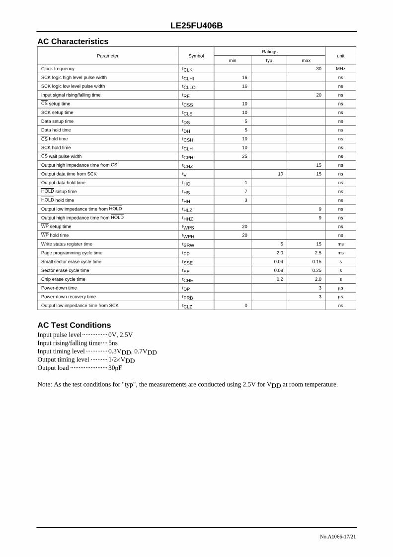
AC Characteristics Ratings
Parameter Symbol min typ max
unit
Clock frequency fCLK 30 MHz
SCK logic high level pulse width tCLHI 16 ns
SCK logic low level pulse width tCLLO 16 ns
Input signal rising/falling time tRF 20 ns
CS setup time tCSS 10 ns
SCK setup time tCLS 10 ns
Data setup time tDS 5 ns
Data hold time tDH 5 ns
CS hold time tCSH 10 ns
SCK hold time tCLH 10 ns
CS wait pulse width tCPH 25 ns
Output high impedance time from CS tCHZ 15 ns
Output data time from SCK tV 10 15 ns
Output data hold time tHO 1 ns
HOLD setup time tHS 7 ns
HOLD hold time tHH 3 ns
Output low impedance time from HOLD tHLZ 9 ns
Output high impedance time from HOLD tHHZ 9 ns
WP setup time tWPS 20 ns
WP hold time tWPH 20 ns
Write status register time tSRW 5 15 ms
Page programming cycle time tPP 2.0 2.5 ms
Small sector erase cycle time tSSE 0.04 0.15 s
Sector erase cycle time tSE 0.08 0.25 s
Chip erase cycle time tCHE 0.2 2.0 s
Power-down time tDP 3 μs
Power-down recovery time tPRB 3 μs
Output low impedance time from SCK tCLZ 0 ns
AC Test Conditions Input pulse level··············· 0V, 2.5V Input rising/falling time···· 5ns Input timing level············· 0.3VDD, 0.7VDD Output timing level ·········· 1/2×VDD Output load ······················ 30pF Note: As the test conditions for "typ", the measurements are conducted using 2.5V for VDD at room temperature.

LE25FU406B
No.A1066-18/21
Figure 20 Status Register Write Flowchart
Status register write
Start
05h Set status register read command
Set status register write command
Program start on rising edge of CS
End of status register write
YES
Bit 0= “0” ?
06h Write enable
01h
NO
* Automatically placed in write disabled state at the end of the status register write
Data

LE25FU406B
No.A1066-19/21
Figure 21 Erase Flowcharts
Start
05h Set status register read command
Set small sector erase command
Address 1
Address 2
Start erase on rising edge of CS
End of erase
Bit 0 = “0” ?
YES
Small sector erase
Address 3
06h Write enable
D7h
NO
* Automatically placed in write disabled state at the end of the erase
Start
05h Set status register read command
Set sector erase command
Address 1
Address 2
Start erase on rising edge of CS
End of erase
Bit 0 = “0” ?
YES
Sector erase
Address 3
06h Write enable
D8h
NO
* Automatically placed in write disabled state at the end of the erase

LE25FU406B
No.A1066-20/21
Figure 22 Page Program Flowchart
Start
05h Set status register read command
Set chip erase command
Start erase on rising edge of CS
End of erase
Bit 0 = “0” ?
YES
Chip erase
06h Write enable
C7h
NO
* Automatically placed in write disabled state at the end of the erase
Page program
Start
05h Set status register read command
Set page program command
Address 1
Address 2
Start program on rising edge of CS
End of programming
YES
Bit 0= “0” ?
Address 3
06h Write enable
02h
NO
* Automatically placed in write disabled state at the end of the programming operation.
Data 0
Data n

LE25FU406B
No.A1066-21/21
PS
This catalog provides information as of January, 2011. Specifications and information herein are subject to change without notice.
SANYO Semiconductor Co.,Ltd. assumes no responsibility for equipment failures that result from usingproducts at values that exceed, even momentarily, rated values (such as maximum ratings, operating conditionranges, or other parameters) listed in products specifications of any and all SANYO Semiconductor Co.,Ltd.products described or contained herein.SANYO Semiconductor Co.,Ltd. strives to supply high-quality high-reliability products, however, any and allsemiconductor products fail or malfunction with some probability. It is possible that these probabilistic failures ormalfunction could give rise to accidents or events that could endanger human lives, trouble that could give riseto smoke or fire, or accidents that could cause damage to other property. When designing equipment, adoptsafety measures so that these kinds of accidents or events cannot occur. Such measures include but are notlimited to protective circuits and error prevention circuits for safe design, redundant design, and structuraldesign.
Upon using the technical information or products described herein, neither warranty nor license shall be grantedwith regard to intellectual property rights or any other rights of SANYO Semiconductor Co.,Ltd. or any thirdparty. SANYO Semiconductor Co.,Ltd. shall not be liable for any claim or suits with regard to a third party'sintellectual property rights which has resulted from the use of the technical information and products mentionedabove.
Information (including circuit diagrams and circuit parameters) herein is for example only; it is not guaranteedfor volume production.
Any and all information described or contained herein are subject to change without notice due toproduct/technology improvement, etc. When designing equipment, refer to the "Delivery Specification" for theSANYO Semiconductor Co.,Ltd. product that you intend to use.
In the event that any or all SANYO Semiconductor Co.,Ltd. products described or contained herein arecontrolled under any of applicable local export control laws and regulations, such products may require theexport license from the authorities concerned in accordance with the above law.No part of this publication may be reproduced or transmitted in any form or by any means, electronic ormechanical, including photocopying and recording, or any information storage or retrieval system, or otherwise,without the prior written consent of SANYO Semiconductor Co.,Ltd.


![[nRF52833] MDBT50-512K & MDBT50-P512K - Version A](https://img.dokumen.tips/doc/110x75/61d2bddca1153d329d4eda55/nrf52833-mdbt50-512k-amp-mdbt50-p512k-version-a.jpg)