Embed Size (px)
Citation preview

Maintenance ManualEDACS®
TEST AND ALARM UNIT (TAU)
LBI-31939E
Printed in U.S.A.ericssonz
Ericsson Inc.Private Radio SystemsMountain View RoadLynchburg, Virginia1-800-528-7711 (Outside USA, 804-528-7711)

Copyright© November 1987, General Electric Company
TABLE OF CONTENTS
SECTION I SYSTEM DESCRIPTION . . . . . . . . . . . . . . . . . . . . . . . . . . . . . . . . . . 2
INTRODUCTION . . . . . . . . . . . . . . . . . . . . . . . . . . . . . . . . . . . . . . . . . . . . . 2
GENERAL DESCRIPTION . . . . . . . . . . . . . . . . . . . . . . . . . . . . . . . . . . . . . . . . 2Alarm/Control Interface Board (A1) . . . . . . . . . . . . . . . . . . . . . . . . . . . . . . . . . 3Display Assembly (A12) . . . . . . . . . . . . . . . . . . . . . . . . . . . . . . . . . . . . . . . 3Logic Board (A4) . . . . . . . . . . . . . . . . . . . . . . . . . . . . . . . . . . . . . . . . . . . 3Serial Interface Board (A13) . . . . . . . . . . . . . . . . . . . . . . . . . . . . . . . . . . . . . 3Mobile Radio . . . . . . . . . . . . . . . . . . . . . . . . . . . . . . . . . . . . . . . . . . . . . 3Control Unit . . . . . . . . . . . . . . . . . . . . . . . . . . . . . . . . . . . . . . . . . . . . . . 3Regulator Board (A7) And Heat Sink Assembly (A8) . . . . . . . . . . . . . . . . . . . . . . . . 3Rear Bulkhead Panel . . . . . . . . . . . . . . . . . . . . . . . . . . . . . . . . . . . . . . . . . 3Power-On Reset Board (A10) . . . . . . . . . . . . . . . . . . . . . . . . . . . . . . . . . . . . 3
CONTROL OF THE TAU . . . . . . . . . . . . . . . . . . . . . . . . . . . . . . . . . . . . . . . . . 3
TEST UNIT OPERATION . . . . . . . . . . . . . . . . . . . . . . . . . . . . . . . . . . . . . . . . 3Control Channel Monitoring . . . . . . . . . . . . . . . . . . . . . . . . . . . . . . . . . . . . . 3Test Call . . . . . . . . . . . . . . . . . . . . . . . . . . . . . . . . . . . . . . . . . . . . . . . . 3
ACU OPERATION . . . . . . . . . . . . . . . . . . . . . . . . . . . . . . . . . . . . . . . . . . . . 3Alarm Reporting . . . . . . . . . . . . . . . . . . . . . . . . . . . . . . . . . . . . . . . . . . . 3Control Output Relays . . . . . . . . . . . . . . . . . . . . . . . . . . . . . . . . . . . . . . . . 4
DIAGNOSTIC SELF TESTS . . . . . . . . . . . . . . . . . . . . . . . . . . . . . . . . . . . . . . . 4
DISPLAY ASSEMBLY . . . . . . . . . . . . . . . . . . . . . . . . . . . . . . . . . . . . . . . . . . 4
USER CALL OPERATING INSTRUCTIONS . . . . . . . . . . . . . . . . . . . . . . . . . . . . . . 4Placing A User Call . . . . . . . . . . . . . . . . . . . . . . . . . . . . . . . . . . . . . . . . . . 4
SECTION II INSTALLATION INSTRUCTIONS . . . . . . . . . . . . . . . . . . . . . . . . . . . . 4
INSTALLATION OF UNIT INTO RACK . . . . . . . . . . . . . . . . . . . . . . . . . . . . . . . . 4
CONNECTION OF USER EQUIPMENT TO ALARM/CONTROL INTERFACE . . . . . . . . . . 5General Provisions . . . . . . . . . . . . . . . . . . . . . . . . . . . . . . . . . . . . . . . . . . 5Input Connections . . . . . . . . . . . . . . . . . . . . . . . . . . . . . . . . . . . . . . . . . . . 5Output Connections . . . . . . . . . . . . . . . . . . . . . . . . . . . . . . . . . . . . . . . . . . 6
PROGRAMMING . . . . . . . . . . . . . . . . . . . . . . . . . . . . . . . . . . . . . . . . . . . . . 6Output Control . . . . . . . . . . . . . . . . . . . . . . . . . . . . . . . . . . . . . . . . . . . . 6Alarm Interpretation . . . . . . . . . . . . . . . . . . . . . . . . . . . . . . . . . . . . . . . . . 6
SECTION III ALARM/CONTROL INTERFACE BOARD . . . . . . . . . . . . . . . . . . . . . . . 6
INTRODUCTION . . . . . . . . . . . . . . . . . . . . . . . . . . . . . . . . . . . . . . . . . . . . . 6Alarm Input Processing . . . . . . . . . . . . . . . . . . . . . . . . . . . . . . . . . . . . . . . . 7
CONTROL OUTPUT PROCESSING . . . . . . . . . . . . . . . . . . . . . . . . . . . . . . . . . . 7
SECTION IV TAU DISPLAY ASSEMBLY . . . . . . . . . . . . . . . . . . . . . . . . . . . . . . . 7
INTRODUCTION . . . . . . . . . . . . . . . . . . . . . . . . . . . . . . . . . . . . . . . . . . . . . 7
OPERATION . . . . . . . . . . . . . . . . . . . . . . . . . . . . . . . . . . . . . . . . . . . . . . . . 7
SECTION V SERIAL INTERFACE BOARD . . . . . . . . . . . . . . . . . . . . . . . . . . . . . . 7
INTRODUCTION . . . . . . . . . . . . . . . . . . . . . . . . . . . . . . . . . . . . . . . . . . . . . 7
POWER CONNECTIONS . . . . . . . . . . . . . . . . . . . . . . . . . . . . . . . . . . . . . . . . . 8
SERIAL LINK . . . . . . . . . . . . . . . . . . . . . . . . . . . . . . . . . . . . . . . . . . . . . . 8ACU Serial Link . . . . . . . . . . . . . . . . . . . . . . . . . . . . . . . . . . . . . . . . . . . 8TU Serial Link . . . . . . . . . . . . . . . . . . . . . . . . . . . . . . . . . . . . . . . . . . . . 8
CONTROL UNIT INTERFACE . . . . . . . . . . . . . . . . . . . . . . . . . . . . . . . . . . . . . 8
SECTION VI LOGIC BOARD . . . . . . . . . . . . . . . . . . . . . . . . . . . . . . . . . . . . . 8
DESCRIPTION . . . . . . . . . . . . . . . . . . . . . . . . . . . . . . . . . . . . . . . . . . . . . . 8
CIRCUIT ANALYSIS . . . . . . . . . . . . . . . . . . . . . . . . . . . . . . . . . . . . . . . . . . 88032 Microprocessor . . . . . . . . . . . . . . . . . . . . . . . . . . . . . . . . . . . . . . . . 8Microprocessor Support Circuitry . . . . . . . . . . . . . . . . . . . . . . . . . . . . . . . . . . 9
Address Latch . . . . . . . . . . . . . . . . . . . . . . . . . . . . . . . . . . . . . . . . . . 10Program And Data Memory . . . . . . . . . . . . . . . . . . . . . . . . . . . . . . . . . . 10Bus Transceiver . . . . . . . . . . . . . . . . . . . . . . . . . . . . . . . . . . . . . . . . . 10Address Decoder . . . . . . . . . . . . . . . . . . . . . . . . . . . . . . . . . . . . . . . . 10Watchdog Timer . . . . . . . . . . . . . . . . . . . . . . . . . . . . . . . . . . . . . . . . . 10
Interface Circuitry . . . . . . . . . . . . . . . . . . . . . . . . . . . . . . . . . . . . . . . . . . 10Serial Interface Board . . . . . . . . . . . . . . . . . . . . . . . . . . . . . . . . . . . . . . 10User RS-232C Terminal (Future Option) . . . . . . . . . . . . . . . . . . . . . . . . . . . 10The Control Interface Board . . . . . . . . . . . . . . . . . . . . . . . . . . . . . . . . . . 10Display-Assembly . . . . . . . . . . . . . . . . . . . . . . . . . . . . . . . . . . . . . . . . 11
SECTION VII REGULATOR BOARD . . . . . . . . . . . . . . . . . . . . . . . . . . . . . . . . . 11
INTRODUCTION . . . . . . . . . . . . . . . . . . . . . . . . . . . . . . . . . . . . . . . . . . . . 11
16 VDC PASS REGULATOR . . . . . . . . . . . . . . . . . . . . . . . . . . . . . . . . . . . . . . 11
10 VDC SWITCHING REGULATOR . . . . . . . . . . . . . . . . . . . . . . . . . . . . . . . . . . 11
5 VDC PASS REGULATOR . . . . . . . . . . . . . . . . . . . . . . . . . . . . . . . . . . . . . . . 11
SECTION VIII TEST AND CHECKOUT . . . . . . . . . . . . . . . . . . . . . . . . . . . . . . . . 11
SCOPE . . . . . . . . . . . . . . . . . . . . . . . . . . . . . . . . . . . . . . . . . . . . . . . . . . 11
ACU . . . . . . . . . . . . . . . . . . . . . . . . . . . . . . . . . . . . . . . . . . . . . . . . . . . . 11
TESTING . . . . . . . . . . . . . . . . . . . . . . . . . . . . . . . . . . . . . . . . . . . . . . . . . 11
MESSAGE INTERPRETATION . . . . . . . . . . . . . . . . . . . . . . . . . . . . . . . . . . . . . 11
FRONT PANEL LEDS . . . . . . . . . . . . . . . . . . . . . . . . . . . . . . . . . . . . . . . . . . 11
DIGITAL CONTROLLER & COMMUNICATIONS PROTOCOL . . . . . . . . . . . . . . . . . . 12
TEST PROCEDURES . . . . . . . . . . . . . . . . . . . . . . . . . . . . . . . . . . . . . . . . . . 12Equipment Required . . . . . . . . . . . . . . . . . . . . . . . . . . . . . . . . . . . . . . . . . 12Test Setup . . . . . . . . . . . . . . . . . . . . . . . . . . . . . . . . . . . . . . . . . . . . . . 12
TU . . . . . . . . . . . . . . . . . . . . . . . . . . . . . . . . . . . . . . . . . . . . . . . . . . . . . 16General Requirements . . . . . . . . . . . . . . . . . . . . . . . . . . . . . . . . . . . . . . . . 16Message Interpretation . . . . . . . . . . . . . . . . . . . . . . . . . . . . . . . . . . . . . . . . 16
DIGITAL CONTROLLER & COMMUNICATIONS PROTOCOL . . . . . . . . . . . . . . . . . . 16Equipment Required . . . . . . . . . . . . . . . . . . . . . . . . . . . . . . . . . . . . . . . . . 16Test Setup . . . . . . . . . . . . . . . . . . . . . . . . . . . . . . . . . . . . . . . . . . . . . . 16
PARTS LIST . . . . . . . . . . . . . . . . . . . . . . . . . . . . . . . . . . . . . . . . . . . . . . . 18
ALARM/CONTROL INTERFACE BOARD OUTLINE DIAGRAM . . . . . . . . . . . . . . . . . 21
LOGIC BOARD OUTLINE DRAWING . . . . . . . . . . . . . . . . . . . . . . . . . . . . . . . . 22
LBI-31939
1

SECTION I SYSTEM DESCRIPTION
INTRODUCTION
The Enhanced Digital Access Communications System(EDACS) Test and Alarm Unit (TAU) is an optional unit at thesite which performs three functions for the EDACS system:
• Remote channel monitoring and testing of EDACSstations.
• Remote reporting of inputs from user-supplied alarmsensors.
• Remote control of relays which operate user-supplieddevices.
Two functional units make up the TAU: the Alarm andControl Unit (ACU) and the Test Unit (TU). The ACU reportsalarm and status input information for control of user-supplieddevices, while testing of the EDACS stations is accomplishedby the TU. The TAU is directed by the Site Controller. A blockdiagram of the TAU and Site Controller interconnections isshown in Figure 1.
GENERAL DESCRIPTION
Most of the modules making up the TAU are located in a19-inch equipment rack. A typical rack installation is shown inFigure 2. Mounted on the front panel of the TAU is the DisplayAssembly, consisting of a polycarbonate display panel, metalpanel frame, Display Board, and associated hardware. Thefront panel is swung down to gain access to the Control Unit
(such as an S-550 EDACS), which is mounted on a bracketattached to the rear of the front panel.TABLE OF CONTENTS (CONT’D)
POWER-ON RESET BOARD OUTLINE DIAGRAM . . . . . . . . . . . . . . . . . . . . . . . . . 22
REGULATOR BOARD OUTLINE DIAGRAM . . . . . . . . . . . . . . . . . . . . . . . . . . . . . 22
SERIAL INTERFACE BOARD OUTLINE DIAGRAM . . . . . . . . . . . . . . . . . . . . . . . . 23
DISPLAY BOARD OUTLINE DIAGRAM . . . . . . . . . . . . . . . . . . . . . . . . . . . . . . . 23
REGULATOR BOARD SCHEMATIC DIAGRAM . . . . . . . . . . . . . . . . . . . . . . . . . . . 24
HEAT SINK ASSEMBLY DIAGRAM . . . . . . . . . . . . . . . . . . . . . . . . . . . . . . . . . . 24
ALARM/CONTROL INTERFACE BOARD SCHEMATIC DIAGRAM . . . . . . . . . . . . . . . . 25
LOGIC BOARD SCHEMATIC DIAGRAM . . . . . . . . . . . . . . . . . . . . . . . . . . . . . . . 28
DISPLAY BOARD SCHEMATIC DIAGRAM . . . . . . . . . . . . . . . . . . . . . . . . . . . . . 31
TAU INTERCONNECTION DIAGRAM . . . . . . . . . . . . . . . . . . . . . . . . . . . . . . . . 33
TAU ASSEMBLY DIAGRAM . . . . . . . . . . . . . . . . . . . . . . . . . . . . . . . . . . . . . . 35
SERIAL INTERFACE BOARD SCHEMATIC DIAGRAM . . . . . . . . . . . . . . . . . . . . . . . 39
LIST OF FIGURES AND TABLES
FIGURE 1 - TEST AND ALARM UNIT . . . . . . . . . . . . . . . . . . . . . . . . . . . . . . . . . 2
FIGURE 2 - TYPICAL TAU RACK INSTALLATION . . . . . . . . . . . . . . . . . . . . . . . . . 2
FIGURE 3 - ACU DISPLAY . . . . . . . . . . . . . . . . . . . . . . . . . . . . . . . . . . . . . . . 4
FIGURE 4 - TYPICAL ALARM INPUT CIRCUIT . . . . . . . . . . . . . . . . . . . . . . . . . . . 5
TABLE 1 - CONTROL OUTPUT CONNECTIONS TO J3 . . . . . . . . . . . . . . . . . . . . . . . 5
TABLE 2 - ALARM INPUT CONNECTIONS TO J4 AND J5 . . . . . . . . . . . . . . . . . . . . . 6
FIGURE 5 - TYPICAL ALARM/CONTROL HOOKUPS . . . . . . . . . . . . . . . . . . . . . . . 7
TABLE 3 - TU AUX STATES . . . . . . . . . . . . . . . . . . . . . . . . . . . . . . . . . . . . . . . 8
TABLE 4 - A AND B SELECT LINE STATES . . . . . . . . . . . . . . . . . . . . . . . . . . . . . 8
TABLE 5 - MICROPROCESSOR SIGNAL LINES . . . . . . . . . . . . . . . . . . . . . . . . . . . 9
FIGURE 6 - LOGIC BOARD FUNCTIONAL DIAGRAM . . . . . . . . . . . . . . . . . . . . . . . 9
TABLE 6 - ADDRESSES AND CONTROLLED CIRCUITS . . . . . . . . . . . . . . . . . . . . . . 10
TABLE 7 - ACU TEST/CHECKOUT PROCEDURE . . . . . . . . . . . . . . . . . . . . . . . . . . 12
TABLE 8 - CONTROL OUTPUT CONNECTIONS TO J3 . . . . . . . . . . . . . . . . . . . . . . . 15
TABLE 9 - ALARM INPUT CONNECTIONS TO J4 AND J5 . . . . . . . . . . . . . . . . . . . . . 16
TABLE 10 - TU TEST/CHECKOUT PROCEDURE . . . . . . . . . . . . . . . . . . . . . . . . . . 17
Figure 1 - Test and Alarm Unit
Figure 2 - Typical TAU Rack Installation
This manual is published by Ericsson Inc., without any warranty, improvements and changes to this manual necessitated bytypographical error, inaccuracies of current information, or improvements to programs and/or equipment, may be made byEricsson Inc., at any time and without notice. Such changes will be incorporated into new editions of this manual. No partof this manual may be reproduced or transmitted in any form or by any means, electronic or mechanical, includingphotocopying and recording, for any purpose, without the express written permission of Ericsson Inc.
LBI-31939
2
When a second swing-down assembly is lowered, accessis gained to the Serial Interface Board and the Logic Board.Access is also gained to the Regulator Board which is mountedin a shielded enclosure on the inside of the rear housing of theTAU. The Alarm/Control Interface Board, Heat Sink Assembly,and the Rear Bulkhead Panel are all accessible from the rearof the TAU. The TU is a mobile radio (such as a RANGREDACS) which is mounted on a shelf.
ALARM/CONTROL INTERFACE BOARD(A1)
Interfacing between the ACU Logic Board and the user-supplied alarms and sensors at the site, is performed by theAlarm/Control Interface Board. This board is mounted at therear of the ACU card cage.
DISPLAY ASSEMBLY (A12)
The Display Assembly is located on the front of the TAU.A Display Panel, Panel Frame, Display Board, and associatedhardware make up this assembly. The Display Board is theactive part of the assembly used to present indications inresponse to commands from the Logic Board.
LOGIC BOARD (A4)
The Logic Board controls the operation of the ACU func-tions within the TAU. It contains an 8032 microprocessorwhich communicates with the Site Controller over an RS-232Clink and controls ACU circuitry. Also contained on the boardare the interface, addressing, and memory circuitry required tosupport the microprocessor.
SERIAL INTERFACE BOARD (A13)
Interfacing between the ACU Logic Board and the SiteController, and between the TU and the Site Controller, isprovided by the Serial Interface Board. This board provideslevel conversion between the Site Controller RS-232C levelsand the open-collector or TTL levels used by the ACU and TU.Switching of the TU between the Site Controller and theControl Unit (such as an S-550 EDACS is also handled by thisboard.
MOBILE RADIO
A mobile radio (such as a RANGR EDACS), with specialfirmware, performs all the Test Unit functions. Interfacingbetween the mobile radio and the Site Controller or the ControlUnit, is handled by the Serial Interface Board.
CONTROL UNIT
When the mobile radio is used in the user-call mode ornormal voice operation, instead of as a test unit, the ControlUnit and microphone are used. The Control Unit connects tothe Serial Interface Board, which provides the required signalsand power between the mobile radio and the Control Unit.
REGULATOR BOARD (A7) AND HEAT SINKASSEMBLY (A8)
Regulated +10 and +5 Volts is provided by the RegulatorBoard. The Regulator Board obtains power from the EDACSstation power supply (nominally 13.8 Vdc), and performs therequired voltage regulation and filtering. Only the +5 voltsupply is used in EDACS applications. Heat sink assembly A8provides the required surface area for dissipating the heatproduced by pass transistors Q1 and Q2.
REAR BULKHEAD PANEL
A Rear Bulkhead Panel is provided for connecting powerto the TAU, and connecting serial links between the Site Con-trollers and the ACU and TU.
POWER-ON RESET BOARD (A10)
The Power-On Reset Board (A10) is a plug-in module thatconnects to the Alarm/Control Interface Board (A1) via J2-13thru 18. This board prevents voltage transients from togglingthe magnetic latching relays on A1 when power is applied tothe TAU. The function is performed by holding MR (MasterReset) at ground potential for approximately 200 to 400 msafter power is applied, to allow the power source to stabilize.
CONTROL OF THE TAU
Operation of the TAU is normally controlled by the SiteController over a 19.2 kilobaud serial data link. Each functionof the TAU (ACU and TU) has its own serial link with the SiteController, and is controlled and operated separately. In addi-tion, each function has a separate serial link with the backupSite Controller. The TU is responsible for switching betweenthe master and backup serial link for both the TU and the ACU.When the TAU is not in service, it may be controlled locally.
TEST UNIT OPERATION
This section describes Test Unit Operation. The TU per-forms the test call function and control-channel monitoring.
CONTROL CHANNEL MONITORING
Monitoring of the control channel at the EDACS site isa primary function of the TAU. When the TU is performingthis function it is in the monitor state. The TU is normally inthe monitor state whenever it is not performing another task.When in the monitor state, the Site Controller issues com-mands which tell the TU the channel number of the controlchannel. The Site Controller then directs the mobile radio totune to the control channel and monitor the messages beingtransmitted. Control channel monitoring consists of the fol-lowing:
• Obtaining sync on the control channel.
• Monitoring the outbound control channel for cor-rectly received messages.
• Verifying the site ID.
When the TU detects a control channel fault, it sends amessage to the Site Controller indicating the type of faultwhich has occurred. At the Site Controller, the faults arelogged and the appropriate action is taken. When the SiteController decides to bring up a new control channel, acommand is issued to the TU giving the number of the newcontrol channel. The TU then attempts to obtain sync on thenew control channel, and if successful, begins monitoringthe new channel.
TEST CALL
When the MOBTX command is issued from the SiteController, the TU performs the Test Call. The Test Call teststhe control channel and the working channel in a simulatedmobile-originated, channel-request sequence. It also checksthe high-speed and low-speed data transmitted over theworking channel. The major steps in the sequence are:
• Site Controller directs the TU to request a channelassignment.
• The TU goes to the control channel, acquires sync,and requests an individual call.
• As directed by the Site Controller, the control chan-nel transmits the assigned working channel.
• The TU receives the channel assignment, goes tothe working channel, and monitors the high speeddata for a channel confirmation.
• The TU sends the high-speed key message followedby the low-speed data.
• The working channel detects the messages from theTU, and transmits low speed data.
• The TU switches to receive and correctly detects thelow-speed data.
• The working channel transmits the drop-channelmessage after two seconds of no transmit activityon channel.
• The TU receives the drop channel message, returnsto the monitor state, and resumes control channelmonitoring.
• The TU keeps track of the progress of the Test Call,and sends the results when it exits the test-call state.
ACU OPERATION
The ACU samples and debounces its alarm inputs andreports changes to the site controller. Additionally, the ACUwill set or reset any combination of its eight relays uponcommand of the site controller. The ACU contains a serialinterface board (also used by the TU) and a Control Unit(used exclusively by the TU). Alarm and relay status arepresented on the front display panel.
ALARM REPORTING
Alarm reporting is one of the functions of the ACU.User-supplied alarm sensing devices may be connected to J4and J5 on the Alarm/Control Interface Board.
Each of the 32 alarm inputs is continually sampled anddebounced, and changes are reported immediately to the sitecontroller through the status message. The status message isalso sent anytime the ACU is polled by the site controller.
There are three alarm masks provided by the site con-troller. These masks define the reporting of the alarms asfollows:
• Enable/disable - A 32-bit mask. A one in any posi-tion represents an alarm which the ACU shouldmonitor. Only changes in state of enabled alarmswill be reported to the site controller.
• Active high/low - A 32-bit mask. A one in anyposition represents an active-high alarm input, anda zero in any position represents an active-lowalarm input.
• Major/Minor alarm - A 32-bit mask. A one in anyposition represents a major alarm input, and a zeroin any position represents an minor alarm input.
LBI-31939
3
All disabled alarms are set to inactive and held thereuntil the alarm is enabled by the site controller. Any changesin state of a disabled alarm are not reported by the ACU.Also, any active high/low or major/minor designation areignored for disabled alarms.
CONTROL OUTPUT RELAYS
Operating the control output relays is the other mainfunction of the ACU. The control outputs provide relaycontact which may be connected to user-supplied devices atthe EDACS site. The relays are under remote control fromthe Site Controller and are set or reset when the SET RE-LAYS message is sent by the site controller. The relay statesare returned to the Site Controller through the status mes-sage.
The output relays are magnetic latching so that powerloss will not cause them to change state. Output relays areactivated by commands from the Site Controller. The currentstate of both the alarm inputs and control outputs can bedetermined at any time by executing the appropriate com-mand at the System Manger. The ACU also compares thecurrent state of the relays to their desired state. If the state isincorrect, an error is displayed on the ACU display panel.
DIAGNOSTIC SELF TESTS
Both the ACU and the TU perform diagnostic self testsafter a reset. If a problem is detected, the ACU or TU willsend a message to the Site Controller, which will log theproblem and take the appropriate action. Since the TAU is amultifunction device, a fault may only partially disable theTAU. Only the function affected will be disabled by the SiteController.
DISPLAY ASSEMBLY
The ACU Display assembly (Figure 3) shows the statusof 32 alarm inputs (ALARM INPUTS), eight relays (CON-TROL OUT), system information (SYS STATUS), and ACUstatus (ALARM UNIT STATUS). When an enabled alarm isactive, the corresponding alarm state indicator is lit. TheCONTROL OUT indicators are turned on when the relay isset (closed). Information from the site controller is displayedby the SYS STATUS indicators as follows:
MAIN CNTRL ACTIVE Indicates the main site controlleris active.
BACKUP CNTRLACTIVE
Indicates the backup site control-ler is active.
ANT PWR FAIL Antenna power failure detectedby the PMU.
CHN PWR FAIL Channel power failure detected.
GETC FAIL GETC logic failure detected.
CHANNEL SETTINGS Indicates GETC switch settingsare incorrect.
INTERCONNECT FAIL Interconnect system failure de-tected.
BACKUP LINK FAIL Indicates failure of backup serialor frame sync link.
System status information is given to the ACU in thesystem status byte each time the site controller is contacted.If the ACU has not received a message after a specified timeinterval, the ACU will turn off the MAIN CNTRL ACTIVEand the BACKUP CNTRL ACTIVE indicators.
The eight SYS STATUS indicators display the internalstatus of the ACU and are continuously updated. Statusinformation is displayed as follows:
MAJOR ALARM Indicates a major alarm is active.
MINOR ALARM Indicates a minor alarm is active.
ACU ERROR Logic error detected.
RELAY ERROR Indicates current relay states donot match designated states.
READY Indicates ACU has received in-itial alarm masks and relay set-tings from the site controller.
POLLED Indicates the ACU has received apoll message from the site con-troller.
NOT READY Lit after ACU power-up or reset.Remains on until the ACU re-ceives initial alarm masks and re-lay set t ings f rom the s i tecontroller.
This ACU status information is also sent to the sitecontroller in the status byte of the status message.
USER CALL OPERATINGINSTRUCTIONS
The mobile radio and Control Unit in the TU may be usedto make calls similar to a normal EDACS mobile. Before a usercall can be initiated, the TU must be in the user-call state.
PLACING A USER CALL
To make a user call:
a. Place the Serial Interface board switch in the SERVposition.
b. Wait for the S-550 EDACS Control Unit displayto illuminate.
c. Proceed with normal mobile operation.
d. Return the microphone to the microphone bracket.
e. Return the slide switch on the Serial InterfaceBoard to the NORM position.
SECTION IIINSTALLATION INSTRUCTIONS
INSTALLATION OF UNIT INTO RACK
Installation of the TAU assembly into the equipment rackis as follows:
1. Mount the TAU in the cabinet. Figure 2 shows thestandard location. (Use of standard locations for equip-ment assures that supplied cables will reach their de-sired connections.)
2. Connect a 19D903880P101 cable between Port 27 onthe back of the Site Controller computer and J2 on therear bulkhead panel of the Alarm and Control Unit.
If there is no PTT activity for several minutes,the TU will remove power from the ControlUnit.
NOTE
Figure 3 - ACU Display
LBI-31939
4

3. Connect a 19D903880P101 cable between Port 28 onthe back of the Site Controller computer and J1 on therear bulkhead panel of the Alarm and Control Unit.
4. Connect a 19D903880P101 cable between Port 27 onthe back of the backup Site Controller computer (ifused) and J4 on the rear bulkhead panel of the Alarmand Control Unit.
5. Connect a 19D903880P101 cable between Port 28 onthe back of the backup Site Controller computer (ifused) and J3 on the rear bulkhead panel of the Alarmand Control Unit.
6. Connect P5 of existing 19A149357G2 power cable toJ5 on the rear bulkhead panel of the Alarm and ControlUnit.
7. Connect #8 red and #8 black wires of 19D901864G2control/power cable to F801B on the 13.8 Vdc stationpower supply.
CONNECTION OF USER EQUIPMENT TO ALARM/CONTROL INTERFACE
GENERAL PROVISIONS
The ACU provides eight control outputs and 32 alarminputs for use with user-supplied control and alarm-sensingdevices. The outputs are SPDT contacts of magnetic latchingrelays, controlled by commands from the Site Controller.
Alarm inputs are optically coupled for isolation, and areconfigured for use with a variety of sensing devices. Alarmstatus information presented to the inputs, is transmitted to theSite Controller for display at the System Manger. The ACUmay be programmed to interpret the alarms as major or minor.The ACU may also be programmed to interpret either the on(logic 1) or the off (logic 0) state of an input as indicating analarm condition. The status of the alarm inputs and controloutputs is displayed on the front of the TAU.
Connections are made via 50-pin connectors on the rearbulkhead of the TAU. The connectors will accept standard25-pair, telephone cable. Typically, a telephone cable will bebrought out to a punch-block where connections to user-sup-plied devices are made. The connections for this arrangementare shown in Tables 1 and 2. The telephone cables and punchblocks are not provided with the TAU.
INPUT CONNECTIONS
A typical circuit of an alarm input is shown in Figure 4.All other inputs are identical. A jumper plug located on theTAU backplane is available for each input to alter the circuitconfiguration. When the jumper is between pins 1 and 2, asshown, the TAU provides 13.8 Vdc from its internal source tothe anode of the LED in the optocoupler. A user-suppliedcontact closure between the cathode (C) and ground (G) inputpins turns on the LED.
The input may also be driven from an external voltage orcurrent source applied between the + and C leads. When theLED is driven from an external source, the current applied tothe LED must not exceed 32 mA. This condition will be metif:
a. The jumper is between pins 2 and 3, and the voltagebetween + and C is less than or equal to 16 Vdc.
OR
b. The jumper is removed, and the voltage between + andC is less than or equal to 48 Vdc.
When the LED is active (conducting) the ACU will readthe input as a logic 0.
NOTE
Figure 4 - Typical Alarm Input Circuit
WIREJACK COLORPIN BASE- BLOCK OUTPUTJ3 TRACE PIN NO. FUNCTION
26 W-BL 11 1 NO1 BL-W 21 1 C NOTES:27 W-O 31 1 NC2 O-W 42 2 NO 1. TABLE SHOWS CONNECTIONS28 W-G 52 2 C FOR A 50 POSITION TYPE 663 G-W 62 2 NC PUNCH BLOCK CONNECTED VIA29 W-BR 73 3 NO A STANDARD 25 PAIR CONNEC-4 BR-W 83 3 C TORIZED CABLE.30 W-SL 93 3 NC5 SL-W 104 4 NO 2. *REQUIRES JUMPER BETWEEN31 R-BL 114 4 C J38-1 AND J38-2 ON THE ALARM/6 BL-R 124 4 NC CONTROL INTERFACE BOARD.32 R-O 135 5 NO7 O-R 145 5 C 3. **REQUIRES JUMPER BETWEEN33 R-G 155 5 NC J39-1 AND J39-2 ON THE ALARM/8 G-R 166 6 NO CONTROL INTERFACE BOARD.34 R-BR 176 6 C9 BR-R 186 6 NC35 R-SL 197 7 NO10 SL-R 207 7 C36 BK-BL 217 7 NC11 BL-BK 228 8 NO37 BK-O 238 8 C12 0-BK 24 8 NC38 BK-G 25 +5V*13 G-BK 26 +5V*39 BK-BR 27 LOG GND14 BR-BK 28 LOG GND40 BK-SL 29 PWR GND15 SL-BK 30 PWR GND41 Y-BL 31 +13.8V**16 BL-Y 32 +13.8V**42 Y-O 3317 O-Y 3443 Y-G 3518 G-Y 3644 Y-BR 3719 BR-Y 3845 Y-SL 3920 SL-Y 4046 V-BL 4121 BL-V 4247 V-O 4322 O-V 4448 V-G 4523 G-V 4649 V-BR 4724 BR-V 4850 V-SL 4925 SL-V 50BL=BLUE O=ORANGE G=GREEN BR=BROWN SL=SLATEW=WHITE R=RED BK=BLACK Y=YELLOW V=VIOLET
Table 1 - Control Output Connections to J3
LBI-31939
5
The minimum LED current necessary to activate the opto-coupler is typically about 7 mA (10 mA maximum). Thus thevoltage ranges for these two cases are about 5 to 16 Vdc withthe jumper in, and 15 to 48 Vdc with the jumper removed.
Current through the LED should drop to zero in the offstate for reliable operation. It is recommended that the LED offcondition be an open circuit.
Connections to the user-supplied devices must be config-ured to maintain the isolation of the TAU. This will insureadequate noise immunity and protection from voltage surges.When the internal 13.8 Vdc supply is used to drive the LED,the user-supplied contact closure must be isolated from the userequipment. A relay with contacts that do not connect to theuser’s equipment is normally adequate. When the userequipment provides the current to the LED, the optocouplerprovides isolation, and connections should only be made topins labeled + and C.
Typical connections between alarm inputs and user-sup-plied devices is shown in Figure 5.
OUTPUT CONNECTIONS
Connections to the control outputs must also maintainisolation between the TAU and user-supplied devices. Theoutput relays provide isolation between their contacts and theTAU. Internal TAU power may be used to drive the load onlywhen the load input circuit provides isolation (e.g., TAU powermay be used with a control output to operate a relay). Systempower is available on the control output connector, however,the total current drawn from this source must not exceed oneampere. When the load power is derived from the load, the onlyconnection to the TAU should be the relay contacts.
The ACU relay contacts are capable of switching resistiveloads of up to one ampere. The user must provide protectionfor the contacts when reactive loads are to be switched. Induc-tive loads, such as a relay, should have a suppression diodeacross the coil. Typical connections of control outputs is shownin Figure 5.
PROGRAMMING
Control of the relay outputs and the interpretation of alarminputs is determined by data stored in the data tables in the SiteController. This data is down loaded to the ACU when the ACUis placed in service. The information field for each type of datais called a mask. The reported alarm condition is comparedwith these alarm tables to determine what action should betaken.
OUTPUT CONTROL
An eight-bit data field, called the output mask (OUTMSK)controls the relays. Each bit in the mask controls one outputrelay. The least significant bit (LSB) controls relay outputnumber one, second LSB controls relay two, etc. When a bit inthe mask is set to one, the corresponding relay is set (normallyopen contacts will close). When a bit in this mask is set to zero,the corresponding relay is reset (normally open contacts willopen).
ALARM INTERPRETATION
The interpretation of the alarm inputs is controlled bythree, 32-bit masks. In each mask, the least-significant bitcorresponds to alarm input number one.
• Enable/disable - A 32-bit mask. A one in any positionrepresents an alarm which the ACU should monitor.Only changes in state of enabled alarms will be re-ported to the site controller.
• Active high/low - A 32-bit mask. A one in any positionrepresents an active-high alarm input, and a zero inany position represents an active-low alarm input.
• Major/Minor alarm - A 32-bit mask. A one in anyposition represents a major alarm input, and a zero inany position represents an minor alarm input.
SECTION IIIALARM/CONTROL
INTERFACE BOARD
INTRODUCTION
The Alarm/Control Interface board is used by the ACUfunction of the TAU. This board provides the interface betweenthe ACU logic and the various user-supplied alarm and controldevices.
Never make a direct connection between the ground orpower circuits in user-supplied equipment and the TAUpower terminals.
NOTE
Never make a direct connection between the ground orpower circuits in user-supplied equipment and the TAUpower terminals.
NOTE
WIREJACK COLOR ALARMPIN BASE- BLOCK NO.J4/J5 TRACE PIN J4 J5 FUNCTION
26 W-BL 1 1 17 +1 BL-W 2 1 17 C NOTES:27 W-O 2 1 17 G2 O-W 4 2 18 + 1. TABLE SHOWS CONNECTIONS28 W-G 5 2 18 C FOR A 50 POSITION TYPE 663 G-W 6 2 18 G PUNCH BLOCK CONNECTED VIA29 W-BR 7 3 19 + STANDARD 25 PAIR CONNEC-4 BR-W 8 3 19 C TORIZED CABLE.30 W-SL 9 3 19 G5 SL-W 10 4 20 + 2. *FOR J4:31 R-BL 11 4 20 C REQUIRES JUMPER BETWEEN6 BL-R 12 4 20 G J40-1 AND J40-2 ON THE ALARM/32 R-O 13 5 21 + CONTROL INTERFACE BOARD.7 O-R 14 5 21 C33 R-G 15 5 21 G *FOR J58 G-R 16 6 22 + REQUIRES JUMPER BETWEEN34 R-BR 17 6 22 C J41-1 AND J41-2 ON THE ALARM/9 BR-R 18 6 22 G CONTROL INTERFACE BOARD.35 R-SL 19 7 23 +10 SL-R 20 7 23 C36 BK-BL 21 7 23 G11 BL-BK 22 8 24 +37 BK-O 23 8 24 C12 O-BK 24 8 24 G38 BK-G 25 9 25 +13 G-BK 26 9 25 C39 BK-BR 27 9 25 G14 BR-BK 28 10 26 +40 BK-SL 29 10 26 C15 SL-BK 30 10 26 G41 Y-BL 31 11 27 +16 BL-Y 32 11 27 C42 Y-O 33 11 27 G17 O-Y 34 12 28 +43 Y-G 35 12 28 C18 G-Y 36 12 28 G44 Y-BR 37 13 29 +19 BR-Y 38 13 29 C45 Y-SL 39 13 29 G20 SL-Y 40 14 30 +46 V-BL 41 14 30 C21 BL-V 42 14 30 G47 V-O 43 15 31 +22 O-V 44 15 31 C48 V-G 45 15 31 G23 G-V 46 16 32 +49 V-BR 47 16 32 C24 BR-V 48 16 32 G50 V-SL 49 G25 SL-V 50 +13.8V*BL=BLUE O=ORANGE G=GREEN BR=BROWN SL=SLATEW=WHITE R=RED BK=BLACK Y=YELLOW V=VIOLET
Table 2 - Control Input Connections to J4 and J5
LBI-31939
6

ALARM INPUT PROCESSING
There are 32 optically-isolated alarm input circuits, eachidentical. Each input circuit may be configured with a jumperto accept either a relay-contact closure, low-voltage (5-16 Vdc)drive, or a high-voltage (15-48 Vdc) drive.
Consider input circuit OC1 on the schematic diagram. Thecircuit consists of resistors R1, R17, and R33; diode D1,optocoupler Q1; and shunt P6. If P6 is connected between J6-1and J6-2 as shown, a relay contact from external equipment canbe connected between J4-1 and J4-27. Closure of this contactwill activate the circuit consisting of R1, P6, R33, and Q1,causing Q1 to conduct.
If P6 is connected between J6-2 and J6-3, a dc voltage canbe applied between J4-26 and J4-1 to activate Q1. Resistor R33will limit the LED (Q1) current to permit operation in the 5-16Vdc range. When P6 is removed entirely, R17 is added to thecircuit. The additional resistance will allow the circuit to bedrive from voltages in the 15-48 Vdc range. In all of the above
cases, when the LED in Q1 lights, the associated transistorturns on. This produces a logic 0 at output pin 5 of the opto-coupler.
The ACU microprocessor determines the status of thevarious alarm inputs by looking at bus DB0 thru DB7. The 32alarm inputs are present at the input of octal, tri-state drivers(U8, U9, U5, and U6) on bus OC1 thru OC32 (optocoupler 1through 32). When eight of the alarm inputs are to be sampled,the proper control work is written to decoder U10. The decodedoutput determines which of the bus drivers is enabled andwhich of the alarm states are placed on the data bus. The DB0
thru DB7 data lines are connected to the Logic Boardthrough connector J1.
CONTROL OUTPUT PROCESSING
Eight DPDT latching relays (K1 thru K8) are used asalarm outputs to control user-supplied equipment. Each re-lay has a set and reset coil which determines the state of therelay contacts. One set of relay contacts is used to presentalarm status to user-supplied equipment through connect J3,the other set of relay contacts reports the relay state back tothe microprocessor. The state of the relays (K1 thru K8) isinput to tri-state drive U6, and output to the data bus (DB0thru DB7) when selected by U10. The check on relay statusis desirable for several reasons:
a. It is proof that the relay does in fact change stateswhen commanded to do so by the microprocessor.
b. Under certain circumstances, the system may "for-get" the existing status of the relays, such as after asystem reset or maintenance. A read of relay statusafter normal operation has resumed will quickly tellwhether or not the relays are in the desired states.They can then be changed as necessary.
When a relay is to be set, the microprocessor places theproper command data on the data bus (DB0 thru DB7) andwrites the proper control word (C1 thru C4) to decoder U10.This allows the SET flip-flop (U3) to latch the set relaypattern. The data is clocked out of U3 and turns on thecorresponding transistors in U1 (an octal Darlington array),which energize the set coil of the proper relay.
After the relay has changed states (latched), the com-mand word on the data bus is changed and the relay is nolonger kept in its energized state. The process for placing therelay in the reset state is the same except that reset flip-flopU4 is selected by decoder U10.
Whenever the microprocessor is reset, master reset MRgoes low, resetting flip-flops U3 and U4. This deenergizesthe set/reset coils of all relays and is designed to protect therelays during system reset and start-up.
SECTION IVTAU DISPLAY ASSEMBLY
INTRODUCTION
The Display Assembly, located on the front panel of theTAU, consists of the Display Panel, the Panel Frame, theDisplay Board, and associated hardware. The Display Panel
provides an LED indication of alarm inputs, control outputs,and ACU and EDACS system status. The LEDs used arelocated on the Display Board, which is mounted directlybehind the Display panel. There is a small window in theDisplay Panel in front of each LED so that the status of theLED may be seen from the front of the TAU.
OPERATION
The Display Board interprets commands from the mi-croprocessor (on the ACU Logic Board) and turns on theappropriate indicator. There are 56 available LED indicators(H1 thru H56) for displaying status information. The LEDsare configured in groups of eight, each tied to the output ofa D flip-flop (U1 thru U5, U11, and U12). The microproces-sor control bus (C1 thru C4) is tied to the input of decoderU15.
When status information is to be displayed, the micro-processor places a command word on the data bus (DB0 thruDB7) indicating which of the indicators is to be turned on.A control work (C1 thru C4) is written by the microprocessorto decoder U15. The decoder enables the proper displayflip-flop where the display information is latched.
Data to be displayed may come from user-suppliedequipment connected to the Alarm/Control Interface Boardor it may come via the serial data link, or be generated insidethe ACU itself. During system reset, MR (master reset) goeslow resetting all flip-flops and turning off all LEDs on theDisplay Board. After normal operation has resumed, themicroprocessor will set the LEDs to their proper states.
SECTION VSERIAL INTERFACE BOARD
INTRODUCTION
The Serial Interface Board is used by both the ACU andTU functions of the TAU. The main function of the SerialInterface Board is to provide serial links between the ACUlogic board and the master (or backup) Site Controller, andbetween the TU and the master (or backup) Site Controller.This board also allows the TU to interface to the ControlUnit, so it may be operated as a regular EDACS mobile. TheSerial Interface Board receives 13.8 Vdc from the externalpower supply, and distributes the power to other boards andassemblies in the TAU.
Figure 5 - Typical Alarm/Control Hookups
Electrical isolation must be maintained between theTAU and user-supplied equipment.
NOTE
LBI-31939
7

POWER CONNECTIONS
Power (13.8 Vdc) is received from the external powersupply via the Rear Bulkhead Panel. The Serial InterfaceBoard then distributes the power to the Regulator Board, theDisplay Assembly, and the Alarm/Control Interface Board.Power is also supplied to the TU mobile and to the ControlUnit. A 2 amp fuse in the mobile and Control Unit lineprovides protection against high currents, while allowing theACU functions to still operate.
SERIAL LINK
The Serial Interface Board receives four independentserial communications links on connector J6. Two links arefrom the master Site Controller, while the other two links arefrom the backup Site Controller. Each link consists of atransmit, receive, and ground line.
The Serial Interface Board provides the necessary leveltranslations required between the RS-232C levels used bythe Site Controllers and the open-collector or TTL levelsused by the ACU and TU. Chip U2 is the RS-232C linedriver, while chip U3 is the RS-232C line receiver. Timer U1is operated as a dc voltage inverter to provide -10 Vdc forchip U2.
ACU SERIAL LINK
The ACU TXD is the transmit serial data line from themicroprocessor on the ACU Logic Board, while ACU RXDis the receive serial data line. The ACU TXD line enters theSerial Interface Board on J5-8, and the signal is routed toboth U2A and U2B for level conversion. From U2A thesignal goes to J6-5, which is the receive data line to themaster Site Controller for the ACU. From U2B the signalgoes to J6-11, which is the receive data line to the backupSite Controller for the ACU. Signals from the ACU arereceived by both the master and backup Site Controllers.
Serial data transmitted from the master Site Controllerfor the ACU enter via J6-4, and go to U3A for level conver-sion. Transmitted serial data from the backup Site Controllerfor the ACU enter via J6-10 and go to U3B. The outputs fromU3A and U3B are connected together, and go to ACU RXDon pin J5-9. Either U3A or U3B is enabled at any given timeby the TU AUX line from the mobile.
The TU AUX line enters the Serial Interface Board onJ2-6, and then splits to go to inverting buffers U4A and U4C.The output of U4A passes through inverting buffer U4B tothe enable pin of U3A. The output of U4C goes to the enablepin of U3B. When TU AUX is at a high logic level, U3A isenabled and ACU RXD receives serial data from the masterSite Controller. When TU AUX is at a low logic level, U3B
is enabled and ACU RXD receives serial data from thebackup Site Controller.
TU SERIAL LINK
The TU TXD is the transmit serial data line from themicroprocessor on the TU mobile, while TU RXD is thereceive serial data line for the TU. Multiplexer U6 controlsthe serial data link connections for the TU. The TU maycommunicate with the master Site Controller, the backupSite Controller or the Control Head.
The TU TXD enters the Serial Interface Board via J2-9,passes through buffer U5A, and goes to Y OUT (IN) of U6.Outputs Y2 and Y3 (U6) are cconnected together and to U2Cand U2D for level translation. The output of U2C goes toJ6-8 for receive serial data from the TU to the master SiteController, while the output of U2D goes to J6-14, forreceive serial data for the backup Site Controller. Again, boththe master and backup Site Controllers receive the serial datafrom the TU.
Serial data transmitted from the master Site Controllerfor the TU enter the Serial Interface Board via J6-7, passthrough U3C for level conversion and go to X2 of U6.Transmitted serial data from the backup Site Controller entervia J6-13, pass through U3D for level conversion, and go toX3 of U6. The X OUT of U6 passes through buffer U5F toTU RXD (J2-8).
Again, TU AUX selects between the master and backupSite Controllers. After passing through U4A, the signal goesto the A SELECT pin of U6. The inputs and outputs enabledby TU AUX are given in Table 3. The state of TU AUX iscontrolled by the TU.
CONTROL UNIT INTERFACE
The Serial Interface Board also allows the TU to beoperated as a regular EDACS mobile. Serial transmit datafrom the Control Unit, CTL HD TXD, enter the SerialInterface Board on J1-4, pass through buffer U5B, and go toboth X1 and X0 of the multiplexer U6. Outputs Y1 and Y0of U6 are coupled together, pass through buffer U5E, and goto J1-5, the receive serial data for the Control Unit (CTL HDRXD).
The TU SER RQST line from the TU enters via J2-4.The signal then passes through buffer U5C to the B SELECTpin of U6. When B SELECT is high, the Site Controller serialdata lines are connected to the TU. When B SELECT is low,the control unit serial data lines are connected to the TU(Table 4). However, when B SELECT is low, TU AUX is stillable to select between the master or backup Site Controllerfor the ACU.
The TU SER RQST also enables power to be provided tothe Control Unit. After the signal passes through buffer U5C,it also passes through inverting buffer U4D to the base oftransistor Q1. When TU SER RQST is low, the output ofinverting buffer U4D is high, and Q1 is turned on. This allowscurrent to flow through the coil of relay K1, and the normallyopen contacts will close, providing 13.8 Vdc at J1-2 (SWA+/CTL HD PWR). When TU SER RQST is high, the outputof U4D is low and Q1 is turned off. The relay then returns toits normally open state. Diode D4 discharges any capacitancefrom relay K1.
When the DPDT slide switch on the Serial Interface Boardis placed in the CTL HD position, 13.8 Vdc is connected toIGN A+ on J2-7, which connects to the TU. This allows the TUto operate as a EDACS mobile. The TU will then cause TU SERRQST to go low.
The speaker on the Serial Interface Board receives itssignals from the mobile via J2-10 and 11.
SECTION VI LOGIC BOARD
DESCRIPTION
The Logic Board directs and coordinates the operation ofthe ACU function of the TAU. During normal operation, the
microprocessor (U1) accepts commands from the Site Control-ler, issues instructions to other ACU circuitry, and sends anacknowledgment signal back to the site controller. If a particu-lar command requires certain data, the microprocessor collectsthe required data, makes necessary decisions based on theresults, and sends a response back to the Site Controller.
The Logic Board consists of an 8032 microprocessor,support circuitry for the 8032, and circuitry required to inter-face the 8032 with the following boards and/or assemblies forthe TAU:
• Serial Interface Board
• Alarm/Control Interface Board
• Display Assembly
Logic Board operation is most conveniently described byusing the segments above as a guideline. Refer to Figure 6 andthe schematic diagrams.
CIRCUIT ANALYSIS
8032 MICROPROCESSOR
The 8032 microprocessor contains:
a. 256 bytes of internal RAM.
Table 3 - TU Aux States
TU AUX STATE INPUT ENABLED OUTPUT ENABLED
High X2-MASTER TXD Y2-MASTER & BACKUP RXD
Low X3-BACKUP TXD Y-3 MASTER & BACKUP RXD
Table 4-A And B Select Line States
B SELECT A SELECT INPUT ENABLED OUTPUT ENABLEDSTATE STATE
Low Low X0-CTL HD TXD Y0-CTL HD RXD
Low High X1-CTL HD TXD Y1-CTL HD RXD
High Low X2-MASTER TXD Y2-MASTER & BACKUP RXD
High High X3-BACKUP TXD Y3-MASTER & BACKUP RXD
LBI-31939
8

b. 32 I/O lines, each of which can be dynamically config-ured to serve as an output or input. Some can addition-ally generate secondary functions such as RD, WR, etc.
c. Three counter/timers which can be made to operate innumerous modes.
d. A six-source, two-priority-level interrupt system withnesting capability.
e. A serial I/O port for multiprocessor communications,I/O expansion, or UART operation.
f. On-chip oscillator and clock circuits.
A description of the microprocessor signal lines used inthis application is given in Table 5.
MICROPROCESSOR SUPPORT CIRCUITRY
The support circuitry consists of the following:
• Address latch
• Program and Data Memory
Fig
ure
6 -
Log
ic B
oar
d F
unct
iona
l Dia
gram
SIGNAL DESCRIPTIONNAME
P00-P07 An eight-bit port used for low-order addressing and data bus.
ALE Address-Latch Enable output used to latch the low-order address byte from P07-P00 into an external latch.
P20-P27 High-order address byte.
PSEN The Program Store Enable output is made active during access to program memory. Allows separation ofdata and program memory. The 8032 can address up to 64K of program memory and up to 64K of datamemory. This dual-address structure simplifies address decoding.
RD Read strobe used to place data from data memory (including memory-mapped I/O) onto the microprocessordata bus (P07-P00).
WR Write strobe used to latch data from the microprocessor into data memory (including memory-mapped I/O).
RESET Resets the microprocessor.
TO Configured as an output line, TO generates a periodic pulse to keep the watchdog timer alive.
RXD Serial data input line which accepts 19.2 kilobaud, asynchronous data from the Serial Interface Board.
TXD A 19.2 kilobaud, asynchronous serial output line from the microprocessor to the Serial Interface Board.
P11 Configured as an input line connected to S2-SW2 (not used).
P12 An input line connected to S2-SW3 (not used).
XTL1 & 2 Connections for the 11.52 MHz crystal.
EA In this application EA is permanently tied low.
Table 5 - Microprocessor Signal Lines
LBI-31939
9

• Bus Transceiver
• Address Decoder
• Watchdog Timer
Address Latch
Port 0 (P07-P00) of the 8032 is time multiplexed, per-mitting it to generate the low-order address byte and to serveas the data bus. Octal latch U2, clocked by the ALE signal,latches the low-order address byte onto the microprocessorbus.
Program And Data Memory
The 8032 microprocessor uses a dual-addressing struc-ture. By using separate read strobes for program memory andfor data memory (PSEN is used for program memory andRD for data memory), a dual address map from 0000-FFFFHex is created.
For example, if the 8032 executes a program instructionread at 0100 Hex the following occurs:
a. The low-order address byte appears on P07-P00 andis latched onto the address bus by U2.
b. The high-order address byte appears on P27-P20,which is part of the address bus.
c. PSEN goes low enabling the output of the addressedEPROM to the data bus.
d. The microprocessor reads the data.
When the 8032 reads RAM at 0100 Hex a similarprocess occurs, except that PSEN remains inactive and RDgoes low. This enables the RAM at that address, while thecorresponding EPROM remains disabled.
The Logic board data memory consists of U4, a 2K x 8bit RAM (at 0000-07FF Hex), and various memory-mappedI/O devices.
Bus Transceiver
Octal bus transceiver U6 is enabled by address bit A15.The direction of the bus transceiver is controlled by RD.When A15 is high (at address
8000 Hex and above) the Microprocessor Data Bus isconnected to the AP Data Bus. The AP Data Bus is used tocommunicate with the:
• Display Board interface circuitry
• Alarm/Control Interface Board interface circuitry
Address Decoder
When the microprocessor reads from or writes to exter-nal data memory or memory-mapped I/O, the proper addressis placed on the address bus. A RD or WR strobe is thenissued to enable the data transfer between the microproces-sor and the addressed device. The Address Decoder acceptsthe appropriate address bits and insures that the deviceaddressed is activated when the RD or WR strobe is asserted.The circuits controlled by the Address Decoder and theiraddresses are listed in Table 6.
The Address Decoder consists of U7 (dual 1-of-4 decoder)and U20E. A decoder is active, when the logical AND of itstwo enable inputs (EA1 and EA2 for side A; EB1 and EB2 forside B) produces a logic one. For example, when the micro-processor loads U9 with a data byte, a write to address A800Hex (binary 1010 1000 0000 0000) is issued. Since A15 equalone, the bus transceiver is enabled and data can be transferredfrom the microprocessor to U9. Since A13 equals one, EA1 andEB1 are both active, but since EA2 and EB2 are inactive, thedecoders are disabled. Note that U7-13 (A0) and U7-3 (A1) areboth low. Because A1 and A0 are both low, the QA0 output ofU7 will follow WR low. Pin U9-11 is the clock input to an octallatch (rising edge trigger), which is connected to QA0. WhenWR again goes high, QA0 and U9-11 follow, latching the datainto the latch as desired. In the previous example, A11 was setto one keeping RAM U4 disabled, preventing a bus-contentionproblem.
Watchdog Timer
A watchdog timer and reset circuit is formed around D3,Q8, and U17. The circuit allows external and manual micro-processor-reset capability. An astable multivibrator is formedfrom a 555 timer (U17). If allowed to run freely, a square wavehaving a period of about 1.5 seconds on output pin U17-3 isgenerated. This pin is connected to RESET pin 9 of the micro-processor. During the 1.5 second period, the voltage on U17-2and U17-6 is varying between 3.33 volts and 1.67 volts. If thevoltage at pins 2 and 6 is held above 3.33 volts, U17-3 willremain low and the microprocessor will not reset. If pins 2 and6 are pulled below 1.67 volts, U17-3 goes high and the micro-processor will reset.
During normal operation, the microprocessor pulses its TOpin periodically. The pulse passes through C22 and turns ontransistor Q3 charging capacitor C21. The pulsing keeps thevoltage at pins 2 and 6 above 3.33 volts, keeping the micro-processor out of reset. If the microprocessor malfunctions, thepulsing of TO will stop and U17 will start. When U17-3 goeshigh, the microprocessor is reset. Since U17 is free running,after a short time U17-3 will go low again, removing the resetfrom the microprocessor. If the microprocessor is reinitialized,TO will again pulse, keeping the microprocessor reset.
The watchdog circuit also has the following capabilities:
a. Manual Reset - When S1 is closed, the voltage at U17-2and U17-6 is pulled below 1.67 volts, resetting themicroprocessor.
b. Watchdog-Timer Disable - Placing a jumper betweenJ9-1 and J9-2 will cause the voltage at pins 2 and 6 tostay above 3.33 volts, disabling the watchdog timer.The circuit will still respond to external and manualresets. This disabling feature is intended as an aid inservicing and should never be used during normal op-eration.
INTERFACE CIRCUITRY
Serial Interface Board
When LOCAL-REMOTE switch 52-SW1 is closed, theLogic Board is placed in the remote mode. Serial informationcan then pass between the Site Controller and the Logic Board,via the Serial Interface Board.
Serial data (LRXD) from the Serial Interface Board, entersthe Logic Board via J3-8 and passes through NAND gatesU18A and U18B to RXD pin 10 of the microprocessor. Serialdata from the microprocessor passes from TXD pin 11 to theSerial Interface Board via J3-7.
User RS-232C Terminal (Future Option)
As a future option in the local mode (S2-SW1 open), auser-supplied RS-232 terminal can be connected via J4 tocheck out the ACU. Serial data from the terminal enters theLogic Board via J4-2. Data then passes through invertinglevel-shifter Q1 and NAND gates U18C and U18B, to the RXDpin of the microprocessor. Data to be sent to the terminaloriginates at the microprocessor TXD pin. Data then passesthrough inverting level shifter Q2 and connector J4-3 to theterminal.
The Control Interface Board
The Alarm/Control Interface Board interface circuitryconsists of control latch U8, tri-state data latch U9, and busdriver U10, each of which can be selected via the AddressDecoder. Transfer of data to and from the Alarm/Control Boardis accomplished by writing the appropriate control informationinto control latch U8. The data written into the latch has thefollowing significance:
BITS FUNCTION
0-2 Select the particular device on the AlarmControl Board to be accessed.
3 Enables the Alarm Control Board decoder.
7 Places the data in U9 onto the AlarmControl data bus.
HEXADECIMAL READ/WRITEADDRESS STATUS FUNCTION
A800 Write Load A/C Interface Board data latch U9.
A801 Write Load A/C Interface Board control latch U8.
A802 Write Load Display Board control latch U11.
A803 Write Load Display Board data latch U12.
A800 Read Enable A/C Data bus to microprocessor via U10.
Table 6 - Addresses And Controlled Circuits
LBI-31939
10

To read data from the Alarm/Control Interface Board, thefollowing procedure can be used:
a. Execute a write to A801 Hex to activate bus transceiverU6 and load control latch U8. Set the data to be loadedas follows; bits 0-2 as required, bit 3 to 1, and bit 7 to0. At the conclusion of the write, alarm/status informa-tion from the Alarm/Control Interface Board will bepresent on the Alarm/Control data bus DB7-DB0.
b. Execute a read to A800 Hex to activate U6 and busdriver U10. The alarm/status information on theAlarm/Control data bus then passes through U10 to theAP data bus, and through U6 to the MicroprocessorData Bus.
A typical write to the Alarm/Control Interface Board canbe performed as follows:
a. Execute a write to A800 Hex to activate bus driver U6and load tri-state data latch U9. The data latched intoU9 will be the actual data sent to Alarm/Control Inter-face Board.
b. Execute a write to A801 Hex to activate U6 and loadcontrol latch U8. Set data bits 0-2 as required, bit 3 to1, and bit 7 to 1 (to place the contents of U9 onto theAlarm/Control data bus).
c. Execute a second write to A801 Hex in exactly the samefashion as in step b, except bit 3 = 0 in this case. Thislatches the data into the selected device on theAlarm/Control Board, completing the data transfer.
Display-Assembly
The Display-Assembly interface circuitry consists of con-trol latch U11 and data latch U12, each of which is selected bythe Address Decoder. Since data is only written to (and neverread from) the Display Assembly, operation is simpler than theAlarm/Control Board interface, though the two cases are quitesimilar.
A typical data write to the Display Assembly can be doneas follows:
a. Execute a write to A803 Hex to load data latch U12 withthe data to be transferred to the board.
b. Execute a write A802 Hex to load control latch U11with the correct control data (bits 0-2 set as required,but 3 set to 1, bits 4-7 set to any state).
c. Execute a write to A802 Hex as in step b, except bit 3= 0. This latches the data into the selected device,completing the data transfer.
SECTION VIIREGULATOR BOARD
INTRODUCTION
The Regulator Board (A7) consists of three separate regu-lators: a 16 Vdc pass regulator (U3), a 10 Vdc switchingregulator (U1), and a 5 Vdc pass regulator. In EDACS applica-tions, only the 5 Vdc output is required to power the logiccircuits; the 16Vdc and 10Vdc outputs are not used. TheEDACS station power supply provides 13.8Vdc (nominal) forthe source voltage to the Regulator Board.
16 VDC PASS REGULATOR
An adjustable three-terminal voltage regulator (U3) pro-vides 16 Vdc at 100 mA from a 24 Vdc source. When the 13.8Vdc source is used, the output is about 11.8 Vdc. The input tothe IC is connected to the +13.8 Vdc line through current-lim-iting resistor R16 and pin 3 of J1. Diode D1 is a 39-volttransient protector connected between the circuit side of R16and ground. This diode shunts any high-voltage spikes that mayappear on the +13.8 Vdc line.
Diode D4 discharges any capacitance on the output of U3if input accidentally shorts to ground. This prevents damage tothe IC due to back-bias overvoltage. Capacitors C16, C17, C20,and C23 act as filter and bypass capacitors. Resistors R21 andR22 adjust the output voltage of the IC according to thefollowing formula:
Vout= 1.25(1 +R1/R2)
10 VDC SWITCHING REGULATOR
Regulator U1 is a regulating pulse-width modulator(PWM) IC. This PWM, along with power Darlington transis-tors Q1 and Q2 are used to provide regulated +10 Vdc at threeamps. This power is available at J2-1 thru 4 and J3-3 (for the5-volt regulator).
The emitters of transistors Q1 and Q2 are supplied +13.8Vdc through filtering and bypassing components C11, L1,C10, C3, C1, and C25. Transient suppression is provided byD1 and R16, and overload shutdown by SCR D6.
The on and off times of Q1 and Q2 are controlled by PWMU1 through base resistors R9 and R10. Base pull-up resistorsR11 and R12 ensure that the transistors are cut off when driveis removed. Both transistors (Q1 and Q2) are driven 180degrees out of phase.
Pulse-width modulator U1 varies the conduction cycleof Q1 and Q2 to maintain a constant output voltage, inde-pendent of load and input voltage variations. When eithertransistor is on, power is drawn from the +13.8 Vdc line andsupplied to the load through L2 at +10 Vdc. During conduc-tion, the voltage at J4-5 is approximately 13.8 Vdc, D3 isreverse biased, and C12 is charging. When the transistorturns off, inductor L2 supplies back emf causing the voltageat J4-5 to go negative. Diode D3 will start conducting andthe load current will flow through D3 and L2. The voltage atJ4-5 is smoothed by the filtering and bypassing componentsL2, C12, L3, C13, C18, and C21 to give a clean +10 Vdcoutput.
The conduction cycle is controlled by U1. The pulsewidth depends on the voltage level at the input to the PWMerror amp (U1-1). Output voltage is sampled at voltagedivider R7 and R3. Pulse-width modulator U1 will changethe pulse width (changing the conduction time of Q1 and Q2)to keep the voltage on pin 1 equal to the reference voltageon pin 2. The voltage on pin 2 is set to 2.5 Vdc by voltagedivider R1 and R2. A +5 Vdc on-chip voltage regulator at pin16 feeds the voltage divider. The frequency of the pulsewidth modulator is set by C5 and R4. Components R6, R8,and C24 are used to phase-compensate and stabilize thefeedback control system.
5 VDC PASS REGULATOR
An adjustable three-terminal voltage regulator IC,mounted on an external heat sink assembly (A8), is used toprovide 5 Vdc AT 1.3A from the +10 Vdc supply. The inputof the regulator is connected to +10 Vdc through J3-3.Capacitors C14, C15, C19, and C22 are used to filter andbypass. Resistors R29 and R18 set the regulator outputvoltage according to the formula: Vout (1 + R18/R19).
SECTION VIIITEST AND CHECKOUT
SCOPE
This section describes how to checkout and test the TAU.Test procedures are divided up into ACU and TU portions ofthe TAU. These test procedures are provided as an aid introubleshooting and as a checkout to verify proper operationafter a repair is made.
ACU
The ACU functions of the TAU are controlled by theLogic Board. Primary functions are to report the state of the32 alarm inputs to the Site Controller and to set or reset theeight control relay outputs upon command from the SiteController. The secondary functions of the ACU are to dis-play the status of the alarm inputs and control outputs on thefront display panel of the TAU, as well as display the ACUstatus and site equipment status.
TESTING
The ACU functions of the TAU are tested by the follow-ing actions.
• The power-up sequence of the ACU is verified andstatus response is sent to master Site Controllerserial link.
• An external digital controller (see equipment list)sends an ACU DIAGNOSTIC command messageto the ACU over master Site Controller serial link.
• The ACU will perform a series of tests on the frontpanel LEDs. These LEDs are observed for correctindications.
• The ACU will set and reset the relays, and theircontrol outputs are monitored.
• The ACU will monitor the alarm inputs, and contactclosures are applied to the alarm inputs. The ACUwill turn on an alarm LED when its correspondingalarm input optocoupler is conducting.
MESSAGE INTERPRETATION
When interpreting ACU response messages, all bytes ofthe message must match the expected response. If any bytedoes not match, it is interpreted as a test failure.
FRONT PANEL LEDS
Follow the FRONT PANEL INDICATOR TEST ex-plained in Table 7.
LBI-31939
11

DIGITAL CONTROLLER &COMMUNICATIONS PROTOCOL
In order to test the TAU, a device must be used that cansend and receive hexadecimal command strings at RS-232Clevels. A digital controller (such as a protocol analyzer) or acomputer with software that allows generation and interpre-tation of the command strings may be used. The term "digitalcontroller" is used throughout this manual to refer to anydevice capable of sending and receiving the required hexa-decimal codes.
The Hex command string (shown as hex command inthe procedure) must be entered. Communications protocol isas follows:
Interface type RS-232C
Data rate 19.2K baud
Data format 1 start bit, 8 data bits, 1 stop bit
MESSAGE FORMAT
FRAME STARTBYTE(AA)
MESSAGE STARTBYTE
DATA BYTES PARITY BYTE
The parity byte is determined by taking the inverse ofthe exclusive-OR of the message start byte with all the databytes.
TEST PROCEDURES
EQUIPMENT REQUIRED
QUANTITY EQUIPMENT TYPE
1 HP 6286A (or equivalent) DC Supplywith current limit
1 Triplett VOM Model 630-PL type 5 (orequivalent)
1 HP 4953A or 4951 C Protocol Analyzer,computer with software to allow genera-tion and reception of hexadecimal com-mand st r ings equivalent d ig i ta lcontroller
2 50-Pin, type 66 punch block or equiva-lent
TEST SETUP
Before testing the ACU, the following setups must bemade:
1. Set S2-1 on the Logic Board to the closed (on)position.
2. Jumper pins 1 and 2 for J6 thru J37 on theAlarm/Control Board.
3. Connect the 16 contact closures for alarms 1 thru 16to J4 on the Alarm/Control Interface Board.
4. Connect the 16 contact closures for alarms 17 thru 32to J5 on the Alarm/Control Interface Board.
5. Open all connections to the alarm inputs.
6. Monitor continuity for the relay control outputs at J3on the Alarm/Control Interface Board.
7. Connect the digital controller to J1 on the Rear Bulk-head panel as follows:
TXD pin on digital controller to J1-3
RXD pin on digital controller to J1-2
GND pin on digital controller to J1-7.
8. Connect the power supply minus (-) lead to J5-1 onthe Rear Bulkhead panel.
9. Connect the power supply positive (+) lead to J5-2on the Rear Bulkhead panel.
10. Turn on power supply and adjust to +13.8 Vdc.
11. Turn off power supply and proceed with test proce-dure in Table 7.
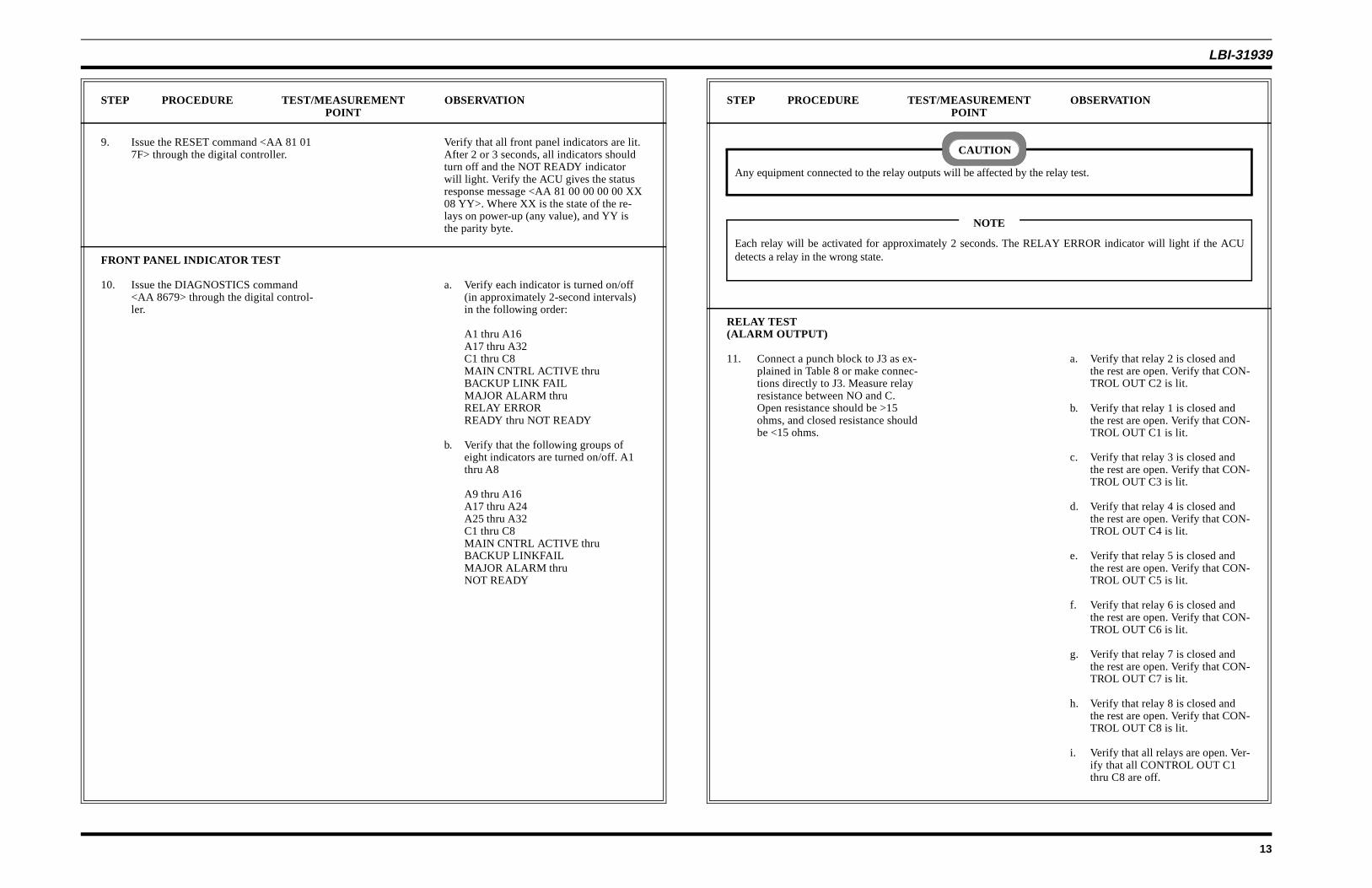
STEP PROCEDURE TEST/MEASUREMENT OBSERVATIONPOINT
CURRENT CHECK
1. Turn on power supply J5-2 Current less than 2 amps
VOLTAGE CHECK
2. Monitor voltage at Rear Bulkhead con-nector using voltmeter.
J2-4J2-5J2-6J2-7J2-8J2-9J2-12
+3.0 to +5.5 Vdc+13.8 Vdc ±20%+3.0 to +5.5 Vdc-0.5 to +0.8 Vdc+3.0 to +5.5 Vdc+3.0 to +5.5 Vdc-0.5 to +0.8 Vdc
REGULATOR BOARD CHECK
3. Monitor voltage at rear bulkhead connec-tor using voltmeter.
J2-4J2-6
+3.0 to +5.5 Vdc+3.0 to +5.5 Vdc
4. Set power supply to +11.0 Vdc and moni-tor voltage using voltmeter.
J2-4J2-6
+3.0 to +5.5 Vdc+3.0 to +5.5 Vdc
5. Set power supply to +16.0 Vdc and moni-tor voltage using voltmeter.
J2-4J2-6
+3.0 to +5.5 Vdc+3.0 to +5.5 Vdc
6. Return power supply to +13.8 Vdc
7. Turn off the power supply.
ACU RESET AND INITIALIZATION
8. Turn on the power supply. Verify status response message <AA 81 0000 00 00 XX 08 YY> to digital controller.Where XX is the state of the relays onpower-up (any value), and YY is the paritybyte.
Diagnostics my be exited at any time by giving the RESET (AA 81 01 7F) command.
NOTE
Table 7 - ACU Test/Checkout Procedure
LBI-31939
12
STEP PROCEDURE TEST/MEASUREMENT OBSERVATIONPOINT
9. Issue the RESET command <AA 81 017F> through the digital controller.
Verify that all front panel indicators are lit.After 2 or 3 seconds, all indicators shouldturn off and the NOT READY indicatorwill light. Verify the ACU gives the statusresponse message <AA 81 00 00 00 00 XX08 YY>. Where XX is the state of the re-lays on power-up (any value), and YY isthe parity byte.
FRONT PANEL INDICATOR TEST
10. Issue the DIAGNOSTICS command<AA 8679> through the digital control-ler.
a. Verify each indicator is turned on/off(in approximately 2-second intervals)in the following order:
A1 thru A16A17 thru A32C1 thru C8MAIN CNTRL ACTIVE thruBACKUP LINK FAILMAJOR ALARM thruRELAY ERRORREADY thru NOT READY
b. Verify that the following groups ofeight indicators are turned on/off. A1thru A8
A9 thru A16A17 thru A24A25 thru A32C1 thru C8MAIN CNTRL ACTIVE thruBACKUP LINKFAILMAJOR ALARM thruNOT READY
STEP PROCEDURE TEST/MEASUREMENT OBSERVATIONPOINT
RELAY TEST(ALARM OUTPUT)
11. Connect a punch block to J3 as ex-plained in Table 8 or make connec-tions directly to J3. Measure relayresistance between NO and C.Open resistance should be >15ohms, and closed resistance shouldbe <15 ohms.
a. Verify that relay 2 is closed andthe rest are open. Verify that CON-TROL OUT C2 is lit.
c. Verify that relay 3 is closed andthe rest are open. Verify that CON-TROL OUT C3 is lit.
d. Verify that relay 4 is closed andthe rest are open. Verify that CON-TROL OUT C4 is lit.
e. Verify that relay 5 is closed andthe rest are open. Verify that CON-TROL OUT C5 is lit.
f. Verify that relay 6 is closed andthe rest are open. Verify that CON-TROL OUT C6 is lit.
g. Verify that relay 7 is closed andthe rest are open. Verify that CON-TROL OUT C7 is lit.
h. Verify that relay 8 is closed andthe rest are open. Verify that CON-TROL OUT C8 is lit.
i. Verify that all relays are open. Ver-ify that all CONTROL OUT C1thru C8 are off.
Any equipment connected to the relay outputs will be affected by the relay test.
CAUTION
Each relay will be activated for approximately 2 seconds. The RELAY ERROR indicator will light if the ACUdetects a relay in the wrong state.
NOTE
b. Verify that relay 1 is closed andthe rest are open. Verify that CON-TROL OUT C1 is lit.
LBI-31939
13

STEP PROCEDURE TEST/MEASUREMENT OBSERVATIONPOINT
ALARM INPUTS TEST
12. Jumper J4-1 and J4-27 are alarm 1. Verify that only indicator A1 is lit.
13. Remove jumper for alarm 1 andjumper J4-28 and J4-3 for alarm 2.
Verify that only alarm indicator A2 islit.
14. Remove jumper for alarm 2 andjumper J4-4 and J4-30 for alarm 3.
Verify that only alarm indicator A3 islit.
15. Remove jumper for alarm 3 andjumper J4-31 and J4-6 for alarm 4.
Verify that only alarm indicator A4 islit.
16. Remove jumper for alarm 4 andjumper J4-7 and J4-33 for alarm 5.
Verify that only alarm indicator A5 islit.
17. Remove jumper for alarm 5 andjumper J4-34 and J4-9 for alarm 6.
Verify that only alarm indicator A6 islit.
18. Remove jumper for alarm 6 andjumper J4-10 and J4-36 for alarm 7.
Verify that only alarm indicator A7 islit.
19. Remove jumper for alarm 7 andjumper J4-37 and J4-12 for alarm 8.
Verify that only alarm indicator A8 islit.
20. Remove jumper for alarm 8 andjumper J4-13 and J4-39 for alarm 9.
Verify that only alarm indicator A9 islit.
21. Remove jumper for alarm 9 andjumper J4-40 and J4-15 for alarm 10.
Verify that only alarm indicator A10 islit.
22. Remove jumper for alarm 10 andjumper J4-16 and J4-42 for alarm 11.
Verify that only alarm indicator A11 islit.
23. Remove jumper for alarm 11 andjumper J4-43 and J4-18 for alarm 12.
Verify that only alarm indicator A12 islit.
24. Remove jumper for alarm 12 andjumper J4-19 and J4-45 for alarm 13.
Verify that only alarm indicator A13 islit.
25. Remove jumper for alarm 13 andjumper J4-46 and J4-21 for alarm 14.
Verify that only alarm indicator A14 islit.
26. Remove jumper for alarm 14 andjumper J4-22 and J4-48 for alarm 15.
Verify that only alarm indicator A15 islit.
A punch block as described in Table 9 maybe used to make connections to the alarm inputs.
NOTE
STEP PROCEDURE TEST/MEASUREMENT OBSERVATIONPOINT
27. Remove jumper for alarm 15 and jumperJ4-49 and J4-24 for alarm 16.
Verify that only alarm indicator A16 is lit.
28. Remove jumper for alarm 16 and jumperJ5-1 and J5-27 for alarm 17.
Verify that only alarm indicator A17 is lit.
29. Remove jumper for alarm 17 and jumperJ5-28 and J5-3 for alarm 18.
Verify that only alarm indicator A18 is lit.
30. Remove jumper for alarm 18 and jumperJ5-4 and J5-30 for alarm 19.
Verify that only alarm indicator A19 is lit.
31. Remove jumper for alarm 19 and jumperJ5-31 and J5-6 for alarm 20.
Verify that only alarm indicator A20 is lit.
32. Remove jumper for alarm 20 and jumperJ5-7 and J5-33 for alarm 21.
Verify that only alarm indicator A21 is lit.
33. Remove jumper for alarm 21 and jumperJ5-34 and J5-9 for alarm 22.
Verify that only alarm indicator A22 is lit.
34. Remove jumper for alarm 22 and jumperJ5-10 and J5-36 for alarm 23.
Verify that only alarm indicator A23 is lit.
35. Remove jumper for alarm 23 and jumperJ5-37 and J5-12 for alarm 24.
Verify that only alarm indicator A24 is lit.
36. Remove jumper for alarm 24 and jumperJ5-13 and J5-39 for alarm 25.
Verify that only alarm indicator A25 is lit.
37. Remove jumper for alarm 25 and jumperJ5-40 and J5-15 for alarm 26.
Verify that only alarm indicator A26 is lit.
38. Remove jumper for alarm 26 and jumperJ5-16 and J5-42 for alarm 27.
Verify that only alarm indicator A27 is lit.
39. Remove jumper for alarm 27 and jumperJ5-43 and J5-18 for alarm 28.
Verify that only alarm indicator A28 is lit.
40. Remove jumper for alarm 28 and jumperJ5-19 and J5-45 for alarm 29.
Verify that only alarm indicator A29 is lit.
41. Remove jumper for alarm 29 and jumperJ5-46 and J5-21 for alarm 30.
Verify that only alarm indicator A30 is lit.
42. Remove jumper for alarm 30 and jumperJ5-22 and J5-48 for alarm 31.
Verify that only alarm indicator A31 is lit.
43. Remove jumper for alarm 31 and jumperJ5-49 and J5-24 for alarm 32.
Verify that only alarm indicator A32 is lit.
44. Remove jumper for alarm 32. Verify that all indicators are off.
LBI-31939
14

STEP PROCEDURE TEST/MEASUREMENT OBSERVATIONPOINT
45. When testing is complete, issue RESETcommand <AA 81 01 7F> through thedigital controller.
BACKUP SERIAL LINK CHECK
46. Disconnect the digital controller cablefrom rear bulkhead connector J1 (masterserial link) and move to J3 (backup se-rial line).
47. Apply 0 V to J1-6 on the Mobile Inter-face Connector Board on the Rear Bulk-head Panel.
48. Issue the RESET command <AA 81017F>
Verify the ACU gives the status response<AA 81 00 00 00 00 XX 08 YY> throughthe digital controller. Where XX is thestate of the relays on power-up (any value),and YY is the parity byte.
WIREJACK COLORPIN BASE- BLOCK OUTPUTJ4/J5 TRACE PIN NO. FUNCTION
26 W-BL 1 1 NO1 BL-W 2 1 C NOTES:27 W-O 3 1 NC2 O-W 4 2 NO 1. TABLE SHOWS CONNECTIONS28 W-G 5 2 C FOR A 50 POSITION TYPE 663 G-W 6 2 NC PUNCHBLOCK CONNECTED VIA29 W-BR 7 3 NO A STANDARD 25 PAIR CONNEC-4 BR-W 8 3 C TORIZED CABLE.30 W-SL 9 3 NC5 SL-W 10 4 NO 2. * REQUIRES JUMPER BETWEEN31 R-BL 11 4 C J38-1 AND J38-2 ON THE ALARM/6 BL-R 12 4 NC CONTROL INTERFACE BOARD.32 R-O 13 5 NO7 O-R 14 5 C 3. **REQUIRES JUMPER BETWEEN33 R-G 15 5 NC J39-1 AND J39-2 ON THE ALARM/8 G-R 166 6 NO CONTROL INTERFACE BOARD.34 R-BR 176 6 C9 BR-R 186 6 NC35 R-SL 197 7 NO10 SL-R 207 7 C36 BK-BL 217 7 NC11 BL-BK 228 8 NO37 BK-O 238 8 C12 O-BK 24 8 NC38 BK-G 25 +5V*13 G-BK 26 +5V*39 BK-BR 27 LOGGND14 BR-BK 28 LOG GND40 BK-SL 29 PWRGND15 SL-BK 30 PWRGND41 Y-BL 31 +13.8 V**16 BL-Y 32 +13.8 V**42 Y-O 3317 O-Y 3443 Y-G 3518 G-Y 3644 Y-BR 3719 BR-Y 3845 Y-SL 3920 SL-Y 4046 V-BL 4121 BL-V 4247 V-O 4322 O-V 4448 V-G 4523 G-V 4649 V-BR 4724 BR-V 4850 V-SL 4925 SL-V 50BL=BLUE O=ORANGE G=GREEN BR=BROWN SL=SLATEW=WHITE R=RED BK=BLACK Y=YELLOW V=VIOLET
Table 8 - Control Output Connections To J3
LBI-31939
15

TU
The TU is tested in two stages. First the mobile radio(which is part of the TU) is tested as a standard mobile radio.Once proper operation of the radio has been determined, theTU interface circuits are tested.
Test the mobile radio by removing the personality EPROMand replacing it with a standard mobile radio personalityEPROM. Then test the radio using its standard test procedure.Refer to the applicable mobile radio Maintenance Manual fordetails on replacing the EPROM and test procedure.
GENERAL REQUIREMENTS
The TU functions of the TAU are controlled by the SystemBoard in the mobile radio. The primary function of the TU isto monitor the signalling on the control channel and reportfailures to the Site Controller. A secondary function of the TUis to permit the mobile radio, when operated in the user-callstate, to be operated as a standard mobile radio.
The TU functions of the TAU are tested by the followingactions:
• The digital controller sends command messages to theTU over the master Site Controller to the TU serialcommunications link.
• The TU sends response messages to the digital con-troller over the same link. These response messagesmust be monitored and interpreted.
• The TU is placed in its user-call state, and a mobilecall is placed and received.
MESSAGE INTERPRETATION
When interpreting TU response messages, all bytes of themessage must match the expected response. If any byte doesnot match, it is interpreted as a test failure.
DIGITAL CONTROLLER &COMMUNICATIONS PROTOCOL
In order to test the TAU, a device must be used that cansend and receive hexadecimal command strings at RS-232Clevels. A digital controller (such as a protocol analyzer) or acomputer with software that allows generation and interpreta-tion of the command strings maybe used. The term "digitalcontroller" is used throughout this manual to refer to any devicecapable of sending and receiving the required hexadecimalcodes.
The Hex command string (shown AS hex command in theprocedure) must be entered. Communications protocol is asfollows:
Interface type RS-232C
Data rate 19.2K baud
Data format 1 start bit, 8 data bits, 1 stop bit
MESSAGE FORMAT
FRAME STARTBYTE(AA)
MESSAGE STARTBYTE
DATA BYTES PARITY BYTE
The parity byte is determined by taking the inverse of theexclusive-OR of the message start byte with all the data bytes.
EQUIPMENT REQUIRED
QUANTITY EQUIPMENT TYPE
1 MASTR® I I Stat ion Power Supply(19D430272G2), or equivalent
1 Triplett VOM Model 630-PL type 5 (orequivalent)
1 HP 4953A or 4951C Protocol Analyzer,computer with software to allow genera-tion and reception of hexadecimal com-mand strings equivalent digital controller
TEST SETUP
Before TU tests are performed, the mobile radio must havethe proper software installed, and the radio must be completelyfunctional. Refer to the mobile radio Maintenance Manual forcomplete test procedures and maintenance information.
1. Attach connector P1 of the mobile power and controlcable to J1 (if RANGR EDACS) of the mobile radio.Connect P2 to J1 of the mobile interface connectorboard, located on the rear bulkhead panel.
2. Connect an antenna to the mobile radio.
3. Connect the TXA+ lead of the mobile power and con-nector cable to the positive (+) terminal of the powersupply. Connect the TX A- lead of the cable to theminus (-) terminal of the power supply.
4. Place switch S1 on the Serial Interface Board in theNORM (open) position.
WIREJACK COLOR ALARMPIN BASE- BLOCK NO.J4/J5 TRACE PIN J4 J5 FUNCTION
26 W-BL 1 1 17 +1 BL-W 2 1 17 C NOTES:27 W-O 3 1 17 G2 O-W 4 2 18 + 1. TABLE SHOWS CONNECTIONS28 W-G 5 2 18 C FOR A 50 POSITION TYPE 663 G-W 6 2 18 G PUNCH BLOCK CONNECTED VIA29 W-BR 7 3 19 + STANDARD 25 PAIR CONNEC-4 BR-W 8 3 19 C TORIZED CABLE.30 W-SL 9 3 19 G5 SL-W 10 4 20 + 2. *FOR J4:31 R-BL 11 4 20 C REQUIRES JUMPER BETWEEN6 BL-R 12 4 20 G J40-1 AND J40-2 ON THE ALARM/32 R-O 13 5 21 + CONTROL INTERFACE BOARD.7 O-R 14 5 21 C33 R-G 15 5 21 G *FOR J58 G-R 16 6 22 + REQUIRES JUMPER BETWEEN34 R-BR 17 6 22 C J41-1 AND J41-2 ON THE ALARM/9 BR-R 18 6 22 G CONTROL INTERFACE BOARD.35 R-SL 19 7 23 +10 SL-R 20 7 23 C36 BK-BL 21 7 23 G11 BL-BK 22 8 24 +37 BK-O 23 8 24 C12 O-BK 24 8 24 G38 BK-G 25 9 25 +13 G-BK 26 9 25 C39 BK-BR 27 9 25 G14 BR-BK 28 10 26 +40 BK-SL 29 10 26 C15 SL-BK 30 10 26 G41 Y-BL 31 11 27 +16 BL-Y 32 11 27 C42 Y-O 33 11 27 G17 O-Y 34 12 28 +43 Y-G 35 12 28 C18 G-Y 36 12 28 G44 Y-BR 37 13 29 +19 BR-Y 38 13 29 C45 Y-SL 39 13 29 G20 SL-Y 40 14 30 +46 V-BL 41 14 30 C21 BL-V 42 14 30 G47 V-O 43 15 31 +22 O-V 44 15 31 C48 V-G 45 15 31 G23 G-V 46 16 32 +49 V-BR 47 16 32 C24 BR-V 48 16 32 G50 V-SL 49 G25 SL-V 50 +13.8V*BL=BLUE O=ORANGE G=GREEN BR=BROWN SL=SLATEW=WHITE R=RED BK=BLACK Y=YELLOW V=VIOLET
Table 9 - Alarm Input Connections to J4 and J5
LBI-31939
16

5. Connect the digital controller to J2 on the rear bulkheadpanel as follows:
TXD pin of digital controller to J2-3RXD pin of digital controller to J2-2GND pin of digital controller to J2-7
6. Connect the minus lead of the power supply to J5-1 onthe rear bulkhead panel. plus lead of the power supplyto J5-2 on the rear bulkhead panel.
7. Perform the TU test procedure in Table 10.
STEP PROCEDURE TEST/MEASUREMENT OBSERVATIONPOINT
CURRENT CHECK
1. Turn on power supply.
2. Monitor voltage using VOM. J2-7 Verify 0 Vdc
POWER-UP AND INITIALIZATION
3. Issue the RESET command <AA FD02> through the digital controller.
Verify TU gives status response of <AA 918000 EE>.
4. Issue the STATUS REQUEST command<AA 07 F8> through the digital control-ler.
Verify TU gives status response of <AA 9181 00 EF>.
5. Issue the status request command <AA07 F8> through the digital controller.
Verify TU gives status response of <AA 9182 00 EC>.
USER-CALL STATE
6. Turn on the trunked radio, and select theproper System and Group.
7. Place S1 on Serial Interface Board in theSERV (closed) position.
a. Verify TU gives status response of AA91 90 00 F4.
b. Verify the Control Unit is on and theSYSTEM and GROUP displays are lit.
8. Select the proper System and Group onthe S-550 EDACS Control Unit
This test requires the use of the EDACS system and one other trunked radio. The TU and trunked radio must be configuredfor the system used for the test.
NOTE
Table 10 - TU Test/Checkout Procedure
STEP PROCEDURE TEST/MEASUREMENT OBSERVATIONPOINT
USER-CALL STATE (CONTINUED)
9. Press the PTT button on the TU ra-dio, and wait for the beep and busyindicator to light.
Audio should be heard from thetrunked radio.
10. Release the PTT button.
11. Press the PTT button on the trunkedradio, and wait for the beep andbusy indicator to light.
Audio should be heard from the TU ra-dio (Serial Interface Board speaker).
12. Release the PTT button.
13. Place S1 on Serial Interface Boardin the NORM (open) position.
a. Verify that the Control Unit dis-plays are off.
b. Verify the TU gives a status re-sponse of <AA 91 82 00 EC>.
CONTROL CHANNEL MONITORING
14. Issue the MONITOR command<AA 08 XX 01 00 00 00 00 00 YY>through the digital controller. WhereXX is the control channel for thetest system, and YY is the paritybyte.
15. Press RESET button on control-channel GETC.
Verify the TU gives the fail response:
AA94XX is 20, 40, or 80ZZ is control channel numberYY is parity
SC STEERING
16. Issue the SC STEERING command<AA 0201 FC> with the backupSite Controller selected.
17. Move the digital controller from J2(Master serial link) to J4 (Backup se-rial link) on the rear bulkhead panel.
18. Issue the status request command<AA 07 F8> through the digital con-troller.
Verify the TU gives the status re-sponse <AA 91 C2 AC>.
19. Issue the RESET COMMAND <AAFD 02> through the digital control-ler or turn power off to exit test.
LBI-31939
17

PARTS LISTLBI-31939
18

PARTS LIST LBI-31939
19

PARTS LISTLBI-31939
20

ALARM/CONTROL INTERFACE BOARD19D901331G3
PARTS LIST OUTLINE DIAGRAM
(19D901331, Sh. 2, Rev. 2)(19D705359, Sh. 1, Rev. 0)
LBI-31939
21

LOGIC BOARD19D901330G3
OUTLINE DIAGRAM
(19D901329, Sh. 1, Rev. 4)(19A704066, Sh 1, Rev. 3)
(19C851503, Rev. 0)(19A704861, Sh. 1, Rev. 0)
POWER-ON RESET BOARD19C851501G1
(19D901040, Sh. 1, Rev. 2)(19A703354, Sh. 1, Rev. 4)REGULATOR BOARD
19D901039G1
(19B801395, Sh. 1, Rev. 0)
LBI-31939
22

SERIAL INTERFACE BOARD19D901848G1
OUTLINE DIAGRAM
DISPLAY BOARD19D901320G1
(19D901322, Rev. 0)(19A704042, Sh. 1, Rev. 0)
(19D901849, Sh. 1, Rev. 0)(19A705098, Sh. 1, Rev. 0)
LBI-31939
23

REGULATOR BOARD19D901039G1
HEAT SINK ASSEMBLY19B801132G1
(19D901176, Rev. 2)
(19B801132, Rev. 2)
LBI-31939
24

ALARM/CONTROL INTERFACE BOARD19D901331G3
(19D901976, Sh. 1, Rev. 1)
SCHEMATIC DIAGRAM LBI-31939
25

ALARM/CONTROL INTERFACE BOARD19D901331G3
(19D901976, Sh. 2, Rev. 1)
SCHEMATIC DIAGRAMLBI-31939
26

ALARM/CONTROL INTERFACE BOARD19D901331G3
(19D901976, Sh. 3, Rev. 1)
SCHEMATIC DIAGRAM LBI-31939
27

SCHEMATIC DIAGRAM
LOGIC BOARD19D901330G3
(19D901363, Sh. 1, Rev. 5)
LBI-31939
28

SCHEMATIC DIAGRAM
LOGIC BOARD19D901330G3
(19D901363, Sh. 2, Rev. 1)
LBI-31939
29

SCHEMATIC DIAGRAM
LOGIC BOARD19D901330G3
(19D901363, Sh. 3, Rev. 1)
LBI-31939
30

SCHEMATIC DIAGRAM
DISPLAY BOARD19D901320G1(19D901362, Sh. 1, Rev. 2)
LBI-31939
31

DISPLAY ASSEMBLY19C851341G2
(19C851341, Rev. 4)
LBI-31939
32

INTERCONNECTION DIAGRAM
TAU INTERCONNECT19D901365G2
(19D901898, Sh. 1, Rev. 2)
LBI-31939
33

INTERCONNECTION DIAGRAM
TAU INTERCONNECT19D901365G2
(19D901898, Sh. 2, Rev. 1)
LBI-31939
34

TAU ASSEMBLY19D901365G1/G2
(19D901365, Sh. 1, Rev. 10)
LBI-31939
35

TAU ASSEMBLY19D901365G1
(19D901365, Sh. 2, Rev. 3)
LBI-31939
36

TAU ASSEMBLY19D901365G2
(19D901365, Sh. 2A, Rev. 3)
LBI-31939
37

TAU ASSEMBLY19D901365G1/G2
(19D901365, Sh. 3, Rev. 7)
LBI-31939
38

SCHEMATIC DIAGRAM
SERIAL INTERFACE BOARD19D901848G1
(19D9018515, Rev. 1,)
LBI-31939
39