Embed Size (px)
Citation preview

Laser Systems and Applications
Cristina Masoller Research group on Dynamics, Nonlinear Optics and Lasers (DONLL)
Departament de Física Universitat Politècnica de Catalunya
[email protected] www.fisica.edu.uy/~cris
MSc in Photonics & Europhotonics

Outline Block 1: Low power semiconductor light sources
Introduction
Semiconductor light sources
LEDs
Amplifiers
Semiconductor lasers
Models
Dynamical effects
Applications

Bibliography
• Saleh and Teich, Fundamentals of photonics (Wiley, Caps. 15
and 16)
• J. M. Liu, Photonic devices (Cambridge 2005, Caps. 12 & 13)
• J. Ohtsubo, Semiconductor lasers: stability, instability and
chaos (Springer, 2n Ed.)
• R. Michalzik, VCSELs (Springer 2013)
3

Acquire a basic knowledge of
• Semiconductor materials and wavelengths
• Operation principles of semiconductor light sources
• Design and fabrication
• Static and dynamics characteristics
• New materials and novel cavity types
10/12/2015 4
Goals

INTRODUCTION
10/12/2015 5

The Nobel Prize in Physics 1956
“For their research on semiconductors and their discovery
of the transistor effect”.
The invention of the transistor at Bell labs in 1947 lead to
the development of the semiconductor industry
(microchips, computers and LEDs –initially only green,
yellow and red) 10/12/2015 6

2012: 50th anniversary of the semiconductor laser
• First demonstration: 1962 (pulsed operation, cryogenic
temperatures).
10/12/2015 7
Robert Hall
Source: Nature Photonics December 2012
• Four research groups in the USA almost
simultaneously reported a functioning
semiconductor laser based on gallium
arsenide crystals (GaAs).
• Three of the papers were published in the
same volume of APL; the other one in PRL - Marshall Nathan of IBM,
- Robert Rediker of MIT,
- Robert Hall and Nick Holonyak from two different
General Electric Company labs.
On the discovery of the diode laser
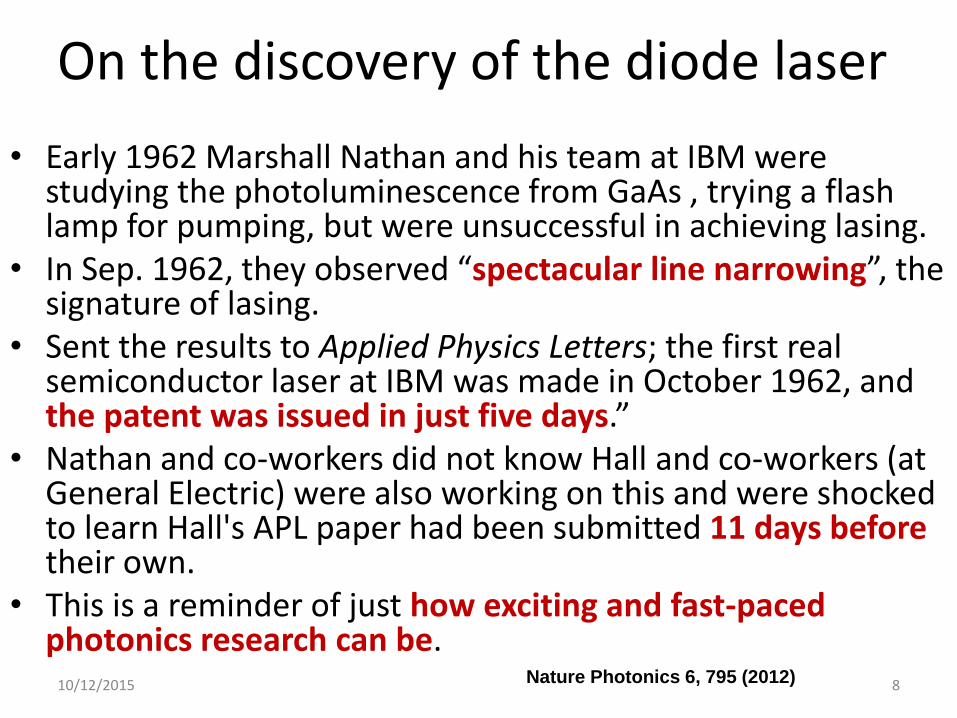
• Early 1962 Marshall Nathan and his team at IBM were studying the photoluminescence from GaAs , trying a flash lamp for pumping, but were unsuccessful in achieving lasing.
• In Sep. 1962, they observed “spectacular line narrowing”, the signature of lasing.
• Sent the results to Applied Physics Letters; the first real semiconductor laser at IBM was made in October 1962, and the patent was issued in just five days.”
• Nathan and co-workers did not know Hall and co-workers (at General Electric) were also working on this and were shocked to learn Hall's APL paper had been submitted 11 days before their own.
• This is a reminder of just how exciting and fast-paced photonics research can be.
10/12/2015 8 Nature Photonics 6, 795 (2012)

10/12/2015 9
• In the 60’ & 70’: diode lasers where “a solution looking for a
problem”.
• Typically: 10–20 years from the initial proof-of-concept of lasing,
often performed at low temperature, until devices useful for
applications are obtained.
• Practical devices require continuous-wave (CW) operation at
room temperature (RT), ideally with direct electrical pumping,
and reasonably long lifetime.
• CW RT emission was achieved in 1970.
• The performance of early diode lasers was limited by
manufacturing techniques.
In the beginnings

The first practical application
10/12/2015 10
• February 1980, an
optical fiber system
was used to
broadcast TV
(Winter Olympics,
Lake Placid, US).
Source: Optics & Photonics News May 2012

After 50 years diode lasers dominate the laser market
• They enable the development of key transformation
technologies with huge social impact.
10/12/2015 11 Source: Laserfocusworld.com

Main application: optical communications
10/12/2015 12
No diode laser No internet!
Source: Infinera
• Needed for long-haul links
• Needed in data centers for >10 Gbits/s box-to-box

Other applications
10/12/2015 13
• Printers, scanners,
sensors, etc.
• Material processing
A dramatic reduction of the
fabrication price made
possible these applications.
• Optical storage: CDs, DVDs and BluRays.
Source: Laserfocusworld.com
(all lasers)

Why diode lasers are so popular?
10/12/2015 14
• Low cost fabrication because of existing semiconductor
technology.
• Electrically pumped, they have low threshold current and
high efficiency.
Each mirror consists of a high-to-low refractive index step
(as seen from inside the cavity)
Adapted from J. Hecht
• Do not require fragile
enclosures or mirror
alignment. • Small size, bright output.
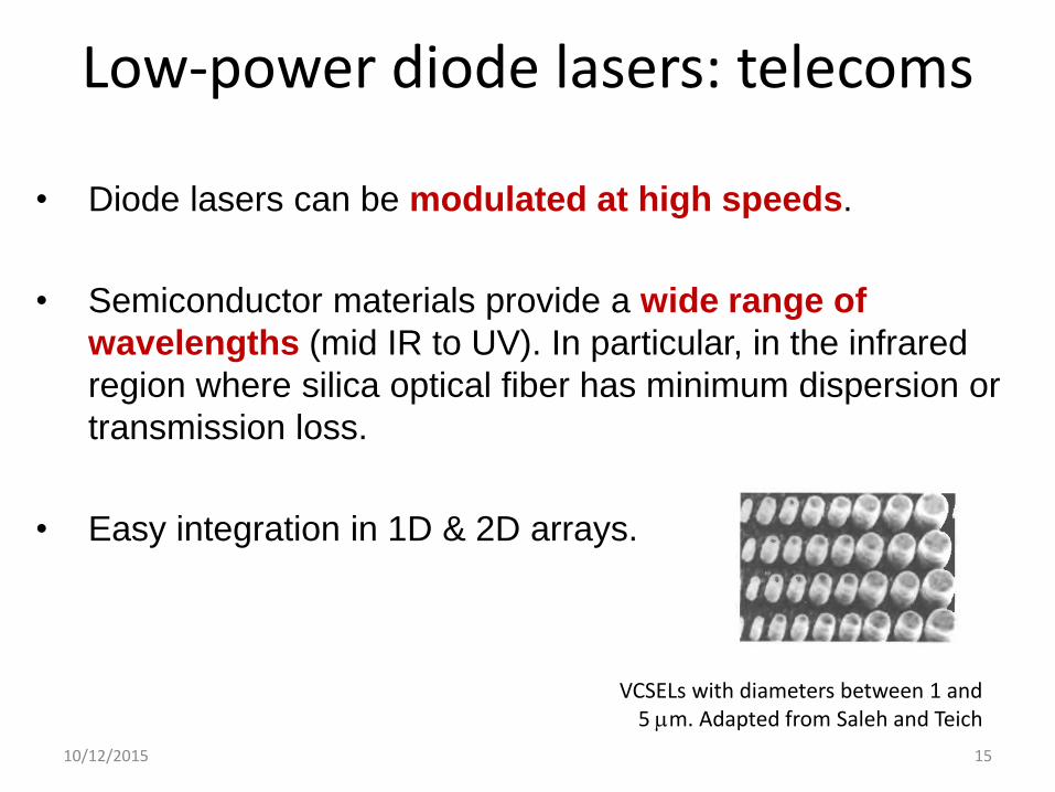
Low-power diode lasers: telecoms
10/12/2015 15
• Diode lasers can be modulated at high speeds.
• Semiconductor materials provide a wide range of
wavelengths (mid IR to UV). In particular, in the infrared
region where silica optical fiber has minimum dispersion or
transmission loss.
• Easy integration in 1D & 2D arrays.
VCSELs with diameters between 1 and 5 m. Adapted from Saleh and Teich

Applications of high-power diode lasers
10/12/2015 16
• Used to pump Erbium Doped Fiber Amplifiers (EDFAs),
which are used in long-distance fiber-optic links.
• Used to pump other lasers
• Solid-state lasers
• Fiber lasers and amplifiers
• Optically pumped semiconductor lasers
• Direct diode industrial applications
• Moderate intensity - Soldering
• High brightness applications – cutting

Outline Block 1: Low power laser systems
Introduction
• Semiconductor materials
• Interactions of photons with electrons & holes
Semiconductor light sources
Models
Dynamical effects
Applications

Basics of semiconductor materials
• Semiconductor material: the bandgap between CB and VB is smaller
than in an isolator (1eV).
• Intrinsic: the semiconducting properties occur naturally.
10/12/2015 18
• Extrinsic: the semiconducting properties
are manufactured.
– Doping: the addition of 'foreign' atoms.
o N-type: has an excess of
electrons.
o P-type: shortage of electrons
(excess of 'holes’)
– Junction effects: join differing materials
together (“compound” semiconductors).
• Direct: light sources
• Indirect: photo-detectors
Adapted from J. Faist

2-level vs. semiconductor material
In a 2-level system: non interacting particles & individual energy levels
In a semiconductor: electron/hole pairs & energy bands
10/12/2015 19
For lasing we need
population inversion:
N2>N1
For lasing we need a large enough
concentration of electrons in the
CB and holes in the VB
Charge neutrality:
Ne Nh N carrier concentration

In a 2-level system: In a semiconductor:
10/12/2015 20
A particle in an excited state
decays emitting a photon A pair electron/hole recombine
emitting a photon; depends on Eg
Conservation of momentum: pe ph (pphoton0) ke kh
Optical transitions are vertical in k space
g = Eg/h, g=c/g g=hc/Eg
2-level vs. semiconductor material

Energy - momentum relation
10/12/2015 21
Near the bottom/top of the conduction/valence bands:
GaAs Si
Gallium arsenide

Direct and indirect semiconductors
10/12/2015 22
Indirect optical transitions (Si,
Ge) inefficient photon sources
(but efficient photo-detectors)
Direct optical transitions
(GaAs) efficient photon
sources
CB
VB
CB
VB
Eg=1.42 eV Eg=1.11 eV
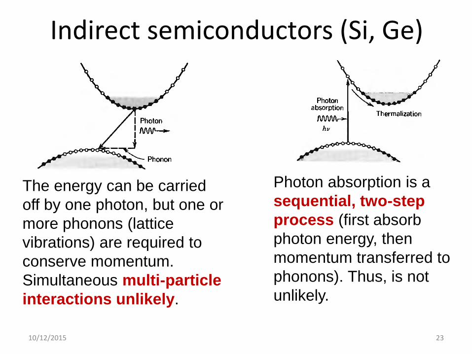
Indirect semiconductors (Si, Ge)
The energy can be carried
off by one photon, but one or
more phonons (lattice
vibrations) are required to
conserve momentum.
Simultaneous multi-particle
interactions unlikely.
10/12/2015 23
Photon absorption is a
sequential, two-step
process (first absorb
photon energy, then
momentum transferred to
phonons). Thus, is not
unlikely.

Quaternary
Semiconductor materials
10/12/2015 24
Elementary Binary: III - V Ternary
Compound semiconductors: by combining different semiconductors,
materials with different optical properties (g, refractive index) can be fabricated.
Almost all the III–V semiconductors
can be used to fabricate lasers
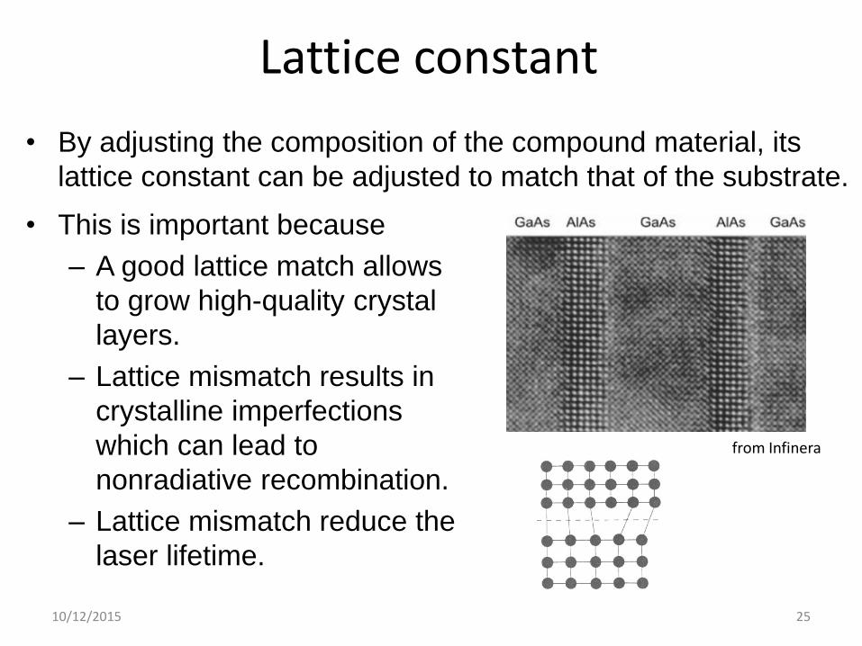
Lattice constant
• By adjusting the composition of the compound material, its
lattice constant can be adjusted to match that of the substrate.
10/12/2015 25
• This is important because
– A good lattice match allows
to grow high-quality crystal
layers.
– Lattice mismatch results in
crystalline imperfections
which can lead to
nonradiative recombination.
– Lattice mismatch reduce the
laser lifetime.
from Infinera

Binary compounds
10/12/2015 26
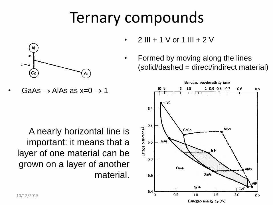
Ternary compounds
10/12/2015 27
• 2 III + 1 V or 1 III + 2 V
• Formed by moving along the lines
(solid/dashed = direct/indirect material)
A nearly horizontal line is
important: it means that a
layer of one material can be
grown on a layer of another
material.
• GaAs AlAs as x=0 1

Quaternary compounds
10/12/2015 28
“y” : is an
extra degree
of freedom
that allows to
adjust both,
the lattice
constant and
the band-gap
The shaded area represents the range of (band-gap, lattice constant)
spanned by the compound (In1-xGax)(As1-yPy).
A quaternary compound is represented
by a point inside the area formed by
the 4 components.

10/12/2015 29
Emission wavelengths of diode lasers
Adapted from J. Hecht

Materials and wavelengths
• UV and blue (445 - 488 nm):
– First developed in the 1990s (more latter)
– GaInN
– Increasing indium increases wavelength
– 405 nm for Blu-ray disks
– 460 nm for blue LEDs and LED lighting
• Green (515-525 nm):
– III-V materials: InGaN on GaN
– II-VI diodes: ZnSe
– Applications: pico-projectors, life sciences
• Red (625-700 nm): AlyGaxIn1-x-yP/GaAs
– Al concentration decreases wavelength
– DVD (650 nm); pointers (635 nm); scanners (635 nm)
10/12/2015 30

Semiconductor materials for blue and green light sources
10/12/2015 31 Adapted from J. Faist (ETHZ)
gallium nitride (GaN)
Other popular option: Zinc Oxide (ZnO is a direct semiconductor)

Materials and wavelengths
• GaAlAs: 750-904 nm
– Al concentration decreases wavelength
– CD players, high-power uses
• InGaAs/GaAs: 915-1050 nm
– In increases wavelength
– Pump lasers (915 nm Yb-fiber; 940 nm Er, Yb; 980 nm Er-fiber)
• InGaAsP/InP diodes: 1100-1650 nm
– First quaternary diodes
– Developed for fiber-optic applications
10/12/2015 32

• The gain, the absorption coefficient, and the refractive index
depend on the electron/hole concentrations.
• Electron/hole concentration can be calculated from
– The density of states
– The probability of occupancy
10/12/2015 33
Optical properties of semiconductors
• Density of states of a
“bulk” material (parabolic
bands; more latter about
non-bulk materials such
as QWs and QDs).
• Joint density of states

10/12/2015 34
Probability of occupancy
Intrinsic semiconductor

Carrier concentrations in thermal equilibrium
10/12/2015 35

Quasi-equilibrium carrier concentrations
10/12/2015 36
• The intra-band relaxation time (ps) is much faster than inter-band
relaxation time (ns).
• When electrical current or photon flux induces band-to-band transitions,
the electrons in CB (and the holes in VB) are thermal equilibrium among
themselves, but they are not in mutual equilibrium: quasi-Fermi levels
(Efc , Efv ) describe each concentration.

Absorption and emission probabilities
Emission probability that a CB
state of energy E2 is occupied by
an electron and a VB state of
energy E1 is empty (occupied by
a hole).
10/12/2015 37
Absorption probability that a CB
state of energy E2 is empty
(occupied by a hole) and a VB
state of energy E1 is occupied by
an electron.
where E2-E1 = h
In thermal equilibrium: fe() < fa()
In quasi-equilibrium, emission is more probable than
absorption if fe() > fa(). This occurs when Efc – Efv > h
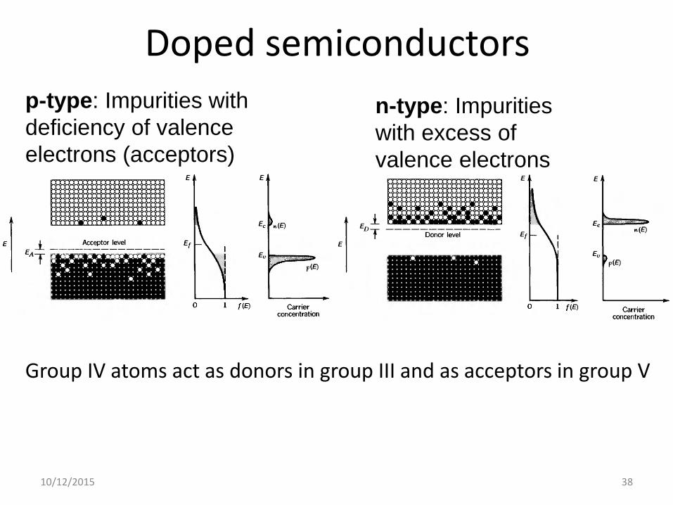
Doped semiconductors
10/12/2015 38
n-type: Impurities
with excess of
valence electrons
(donors)
p-type: Impurities with
deficiency of valence
electrons (acceptors)
Group IV atoms act as donors in group III and as acceptors in group V

The p-n junction Before contact After contact
10/12/2015 39
• Mobile electrons and holes diffuse.
• Leave behind a region (“depletion layer”) that
contains only fixed charges
• These fixed charges create an electric field
that obstructs the diffusion of mobile charges.

The biased p-n junction • By applying a positive voltage to
the p-region, the electric field
changes direction and current
can flow across the junction.
10/12/2015 40
The p-n junction
acts as a diode
First semiconductor lasers were p-n junctions (“Homo-structures” )
• Recombination at junction: converts current into light.
• Concentrating current and light improves the efficiency.

PHOTONS IN SEMICONDUCTORS
-SEMICONDUCTOR MATERIALS
-INTERACTIONS OF PHOTONS WITH ELECTRONS
AND HOLES
10/12/2015 41

Photon/carrier interactions in a semiconductor
• Inter-band (Band-to-band):
– absorption
– stimulated emission
– spontaneous emission
• Intra-band (Quantum cascade lasers)
• Others:
─ Impurity-to-band (Shockley–Read)
─ Excitonic (exciton: e/h pair held together by their
Coulomb attraction ─like a hydrogen atom but
with a hole instead of a proton. More latter about
exciton-polariton lasers)
─ Auger (electron-hole + third carrier)
─ Phonon (long wavelength photons excite directly
lattice vibrations -phonons)
10/12/2015 42

Carrier recombination processes
10/12/2015 43 Adapted from J. M. Liu (Photonic Devices)
Carrier
capture by an
impurity.
It can be
radiative or
nonradiative
depending on
the type of
impurity
- band-to-band
- exciton
Non-radiative
recombination:
the energy
released by
band-to-band
recombination of
an e/h pair is
picked up by a
third carrier.
• Shockley–Read recombination: one carrier at a time.
• Bimolecular recombination: e/h simultaneously.
• Auger
• A photon emitted by band-to-band recombination has an
energy slightly higher than the bandgap.
• A photon emitted through a process involving the impurities
(SR recombination) has an energy lower than the bandgap.

Shockley–Read radiative recombination through impurity states
• Is important in indirect-gap semiconductors, in which band-to-
band radiative recombination probabilities are very low.
10/12/2015 44
• For example, N and ZnO
impurities in GaP act as
electron traps.
• In particular, this process is
responsible for improving the
luminescence efficiency of the
indirect-gap semiconductors
for their applications as
materials for LEDs.

Carrier recombination rate
10/12/2015 45
32 CNBNANR
Spontaneous carrier
recombination lifetime: nrr
CNBNAN
R
111 2
Radiative and nonradiative
recombination rates
Adapted from J. M. Liu (Photonic Devices)

Internal quantum efficiency
10/12/2015 46
Fraction of the injected electron flux that is converted
into photon flux: radiative / total recombination rate.
in = (1/r) / (1/)
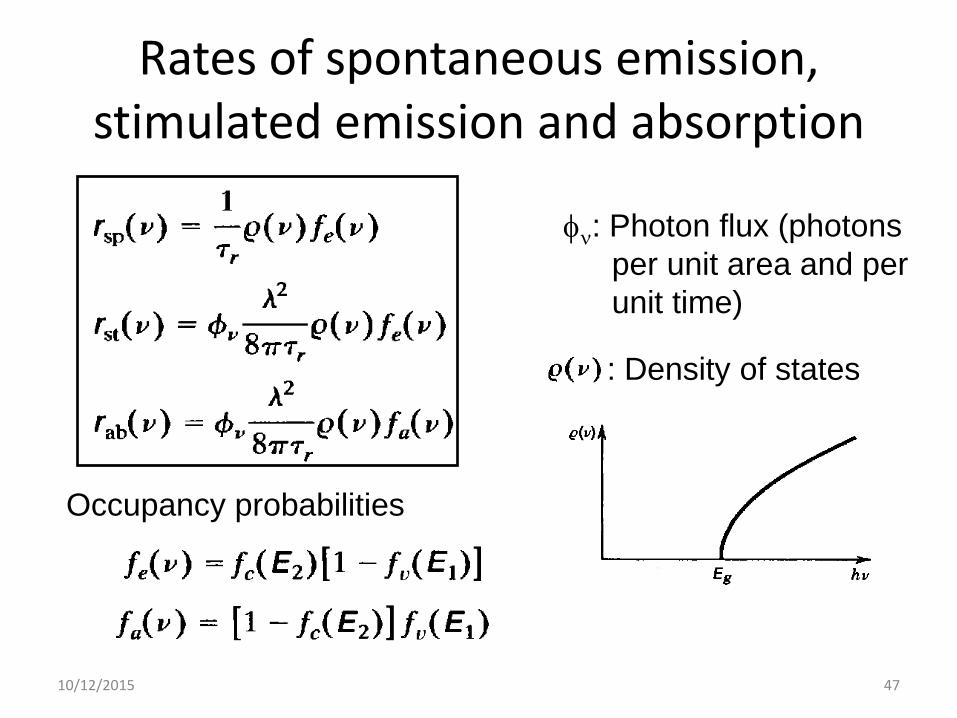
Rates of spontaneous emission, stimulated emission and absorption
10/12/2015 47
: Photon flux (photons
per unit area and per
unit time)
: Density of states
Occupancy probabilities

All optical transitions contribute to the absorption coefficient
10/12/2015 48

Absorption coefficient of several semiconductor materials
10/12/2015 49

Semiconductor gain G(N,,T)
10/12/2015 50
RT InGaASP laser Net gain coefficient
Net gain coefficient = (rates of stimulated
emission – absorption) / incident photon flux
50 nm
The semiconductor gain
spectrum is asymmetric.
Carrier
concentration (N) Gain width depends of
the carrier concentration and the temperature.
N
0 = a (N-N0)
N0 : carrier
concentration at
transparency
a depends on

Refractive index n(N,,T)
• Is related to gain by the Kramers-Kroning relations
[gain ─ Im(), n Re()] n also depends on N, , T.
10/12/2015 51
At T=300 K
The peak in the high-purity curve is
associated to free excitons.
GaAs at T=300 K

10/12/2015 52
The electron/hole concentration
in the depletion layer modifies
the refracting index, creating a
wave guide that helps to
confine the photons
Carrier-induced waveguide
The first generation of diode lasers were “homo-junctions”

Thermal effects
10/12/2015 53
GaAs InP
At 300 K:
Adapted from J. M. Liu, Photonic devices
• Temperature affects the gain (the peak and the width).
• This causes a variation of the refractive index [via the
Kramers-Kronig relations: gain ─ Im(), n Re()].

TF test Si and Ge are important materials for photo-detectors but are not
useful as light sources.
The composition of ternary compounds can be varied to adjust both,
the lattice constant and the band-gap.
The composition of quaternary compounds can be varied to adjust
both, the lattice constant and the band-gap.
The electron/hole occupancy probabilities in the conduction/valence
bands are independent of the temperature.
The length of the “depletion layer” depends on the diffusion length of
electrons and holes.
In a semiconductor the refractive index is independent of the carrier
concentration.
The “depletion layer” acts as a waveguide for confining the photons.
10/12/2015 54

Outline Block 1: Low power semiconductor light sources
Introduction
Semiconductor light sources
LEDs
Amplifiers
Lasers
New materials and cavity designs
Models
Dynamical effects
Applications

10/12/2015 56
Photo-detectors LEDs Lasers & amplifiers
Band-to-band transitions: absorption, spontaneous and stimulated recombination
LEDs operation principle: spontaneous recombination

10/12/2015 57
• The light’s wavelength depends on the material used.
• LED’s size < a grain of sand.
Electro-luminescence (inverse of the photo-electric effect)
Green, yellow and red versions were invented in the 1950s and
were used in calculator displays, “on/off” light indicators, etc.

The 2014 Nobel Prize in Physics
“for the invention of efficient blue LEDs which has enabled
bright and energy-saving white light sources”
10/12/2015 58
Isamu Akasaki
Nagoya University
Japan
Shuji Nakamura
University of California
Santa Barbara, US
Hiroshi Amano
Nagoya University
Japan

10/12/2015 59
Based on gallium nitride (GaN), blue LEDs are combined
with fluorescent materials to realize white light.
Blue LED: how does it work?

10/12/2015 60
• About ¼ of world electricity consumption is used for lighting.
• The highly energy-efficient LED lamps contribute to saving
up to 20% of the global electricity consumption.
LED lamps are very efficient!
Why the Nobel Price?

10/12/2015 61
Nature Photonics April 2007
Blue lasers — also invented by Akasaki and Amano, and separately by
Nakamura — are being used in Blu-ray Disc technology.
Future applications:
Blue LEDs for portable devices that disinfect or sterilize water; also for
computer optical memory.
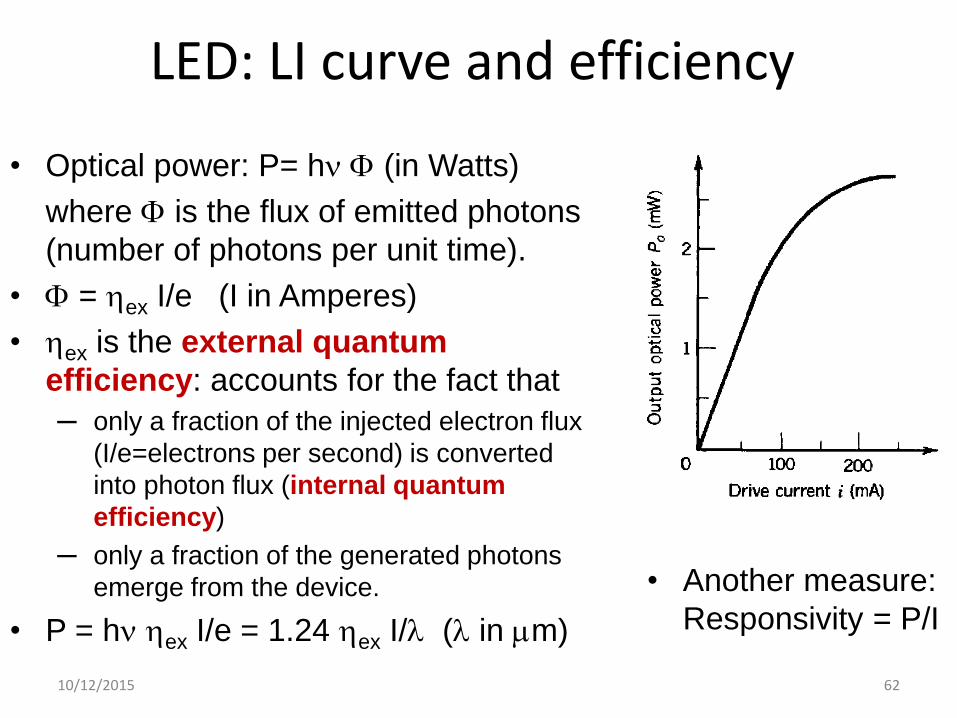
LED: LI curve and efficiency
10/12/2015 62
• Optical power: P= h (in Watts)
where is the flux of emitted photons
(number of photons per unit time).
• = ex I/e (I in Amperes)
• ex is the external quantum
efficiency: accounts for the fact that
─ only a fraction of the injected electron flux
(I/e=electrons per second) is converted
into photon flux (internal quantum
efficiency)
─ only a fraction of the generated photons
emerge from the device.
• P = h ex I/e = 1.24 ex I/ ( in m)
• Another measure:
Responsivity = P/I

LED: structures
Surface-emitting Edge-emitting
10/12/2015 63
Light emitted from the
opposite face is either
absorbed or reflected.
Burrus-type
LED: light is
collected
directly from the
active region
(efficient
coupling into an
optical fiber).
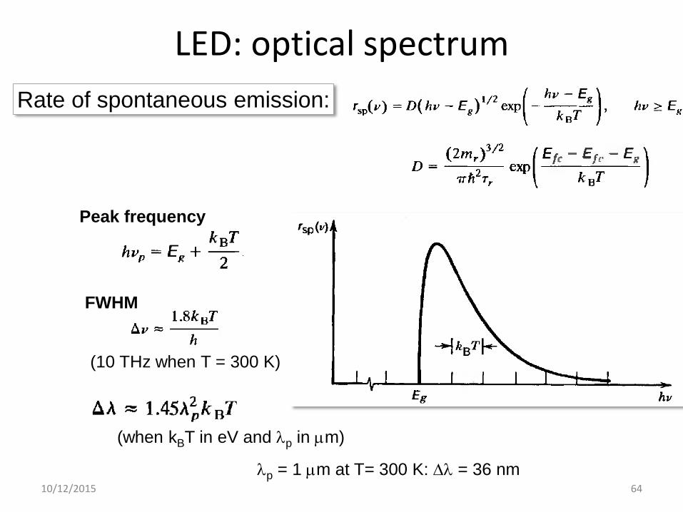
LED: optical spectrum
10/12/2015 64
Rate of spontaneous emission:
Peak frequency
FWHM
(when kBT in eV and p in m)
(10 THz when T = 300 K)
p = 1 m at T= 300 K: = 36 nm

Spectrum vs wavelength
10/12/2015 65

SEMICONDUCTOR LIGHT SOURCES LEDS, AMPLIFIERS AND DIODE LASERS
10/12/2015 66
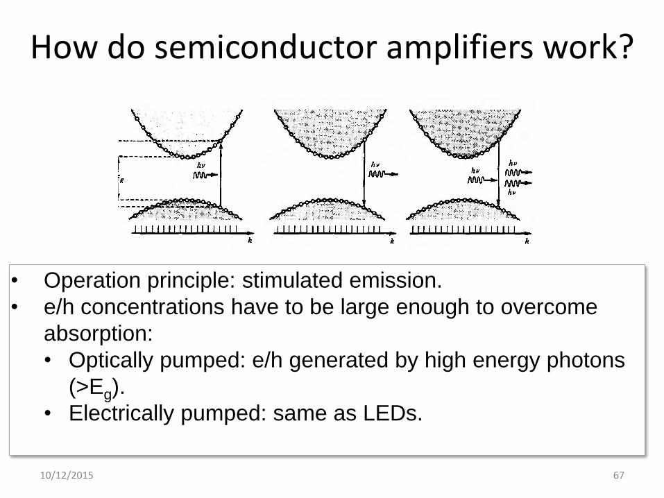
How do semiconductor amplifiers work?
10/12/2015 67
• Operation principle: stimulated emission.
• e/h concentrations have to be large enough to overcome
absorption:
• Optically pumped: e/h generated by high energy photons
(>Eg).
• Electrically pumped: same as LEDs.

Amplifier bandwidth
68
Density of states
Fermi inversion factor
(solid T=0, dash RT)
Gain coefficient
(solid T=0, dash RT)

d
L
Injected current density
10/12/2015 69
1/ x N =
J= i / (wL) (Ampere per unit area)
Steady-state injection condition:
Recombination rate x carrier
concentration = injection rate
(i/e)/(w d L)
w10 m
L200 m
d 0.1-2m
internal quantum efficiency: fraction
of the injected electron flux that is
converted into photon flux
in = (1/r) / (1/) 1/ = 1/(in r)
1/ (in r ) N = (i/e)/(w d L) = J/(ed) J = e d N / (in r)
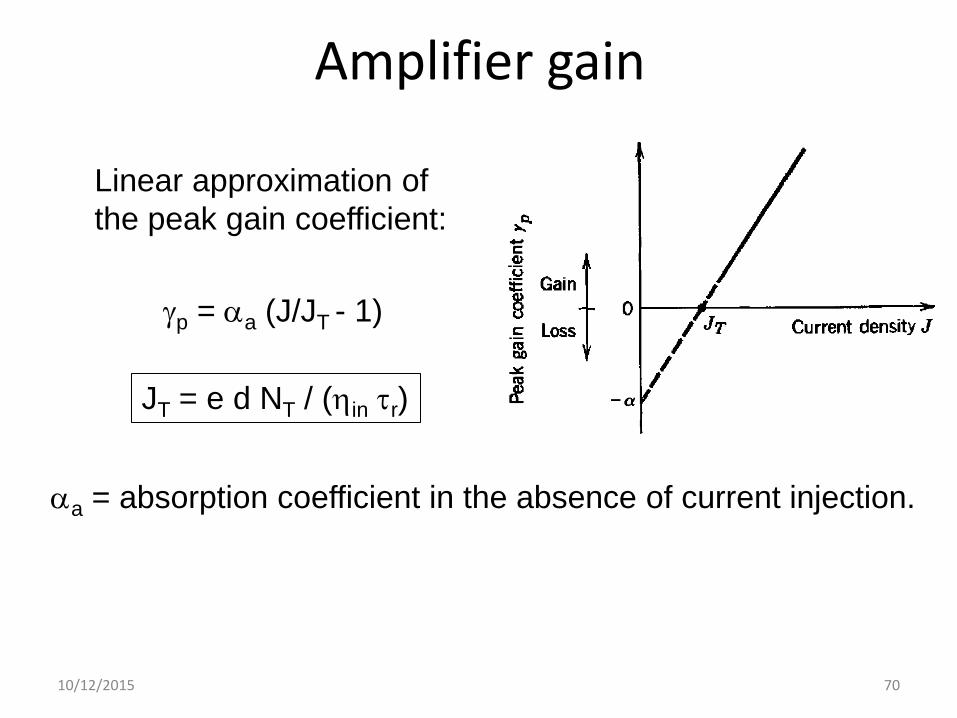
Amplifier gain
Linear approximation of
the peak gain coefficient:
p = a (J/JT - 1)
10/12/2015 70
a = absorption coefficient in the absence of current injection.
JT = e d NT / (in r)

Exercise
An InGaAsP amplifier operates at 300 К with the following
parameters:
in =0.5, r = 2.5 ns, N0 = 1.25 1018 cm-3 (transparency
carrier concentration), a=600 cm-1, w=10 m, L=200
m, d =2 m.
– Calculate the transparency current density.
– Calculate the peak gain coefficient and the amplifier gain
when J = 3.5 104 A/cm2.
– Calculate the injection current required to produce this
current density.
10/12/2015 71

10/12/2015 72
• N0 is the carrier concentration for transparency.
• JT is proportional to the active region thickness (d).
• Reducing d will reduce the threshold current.
• However, carrier diffusion prevents from confining
electrons and holes in too small regions (their diffusion
lengths are several m).
• Can we confine the carriers to a region whose thickness
is smaller than the carrier diffusion length?
• Yes. By using “hetero-structures”.
• The second-generation of semiconductor lasers were
hetero-structures.
Threshold and active region thickness
JT = e d N0 / (in r)

10/12/2015 73
Double Heterostructures (DH)
Semiconductors with different band-
gaps: improved e/h confinement
Improved photon confinement:
“built-in” waveguide because
the semiconductors have
different refractive index
From K. Kieu (University of Arizona)
p-n junction:
the depletion
layer acts as
a waveguide

Example of DH structure
• Improved photon
confinement due to the larger
index of refraction of GaAs (n =
3.6) compared to the p- and n-
cladding layers (n = 3.4).
• Improved carrier
confinement due to the
smaller band gap (Eg ≈ 1.5 eV)
of GaAs compared to the p-
and n- cladding layers (Eg ≈ 1.8
eV).
10/12/2015 74 Source: Thorlabs tutorial

The 2000 Nobel Prize in Physics
“For basic work on information and
communication technology"
“For developing semiconductor
heterostructures used in high-speed
opto-electronics"
10/12/2015 75
Zhores I. Alferov Iaffe Physico-Technical
Institute, St. Petersburg Russia
Herbert Kroemer University of California
USA
The improved photon – electron/hole confinement of DH lasers
allowed for cw RT emission, enabling the development of
technologies with huge social impact.

Drawback: DHs are more
complicated to fabricate: they
require strict matching
conditions between the two
semiconductor layers (the lattice
constant and the thermal
expansion coefficient).
10/12/2015 76
DH technology: lower threshold
Early 1980s: moving the DH technology one step further to quantum-wells (QWs)
QW lasers are DH lasers (also referred to as “bulk” lasers) but
the thickness of the active layer is so narrow (< 50 nm) that
the energy-momentum relation of bulk material does not apply.
• Compared to a DH, a QW has very poor optical wave-guiding
ability because of its small thickness.
• Using multiple quantum wells (MQS) helps to improve optical
wave-guiding.
• To have really good optical confinement, separate confinement
hetero-structures are used.
77

QW energy levels
10/12/2015 78
In a QW laser the carriers are confined in the x direction within a
distance d1 (well thickness). But, in the plane of the active layer (y—z plane), they behave as in a bulk semiconductor.
1D infinite potential:

Gain coefficient: QW vs DH
Density of states
10/12/2015 79
Peak gain coefficient
In QWs JT is several times
smaller than comparable DHs.

Multiple Quantum Well (MQW)
• Alternating QW material (narrow band gap)
with barrier material (high band gap).
• Advantages:
– Dramatic reduction in threshold current
– Reduction in carrier loss
– Reduced temperature sensitivity of
threshold current
– Increase laser efficiency
– Reduce thermal resistance
– Higher output power
• Drawback: increased fabrication cost
10/12/2015 80

Novel materials include quantum-wire, quantum-dash and quantum-dots
10/12/2015 81

Fabrication techniques
Epitaxial grow, as layers of one material over another, by
– molecular-beam epitaxy (MBE) uses molecular beams of
the constituent elements in a high-vacuum environment
(10-8 Pa),
– liquid-phase epitaxy (LPE) uses the cooling of a
saturated solution containing the constituents in contact
with the substrate (but layers are thick),
– vapor-phase epitaxy (VPE) and metal-organic chemical
vapor deposition (MOCVD) use gases in a reactor. The
growth is by chemical reaction (not as MBE, by physical
deposition).
10/12/2015 82
Advances in these techniques were
crucial for lowering fabrication costs.

Molecular-beam epitaxy
10/12/2015 83 Adapted from J. Faist, ETHZ
The compositions and dopings of the individual layers are
determined by manipulating the arrival rates of the molecules
and the temperature of the substrate surface.
Individual layers can be made very thin (atomic layer accuracy)
Alfred Y. Cho
“spray painting...
with atoms”
(The New York
Times, 1982)

Modern MBE
10/12/2015 84
Adapted from J. Faist, ETHZ

ATG (Asaro-Tiller-Grinfeld) instability
• Also known as the Grinfeld instability.
• It is an elastic instability that often occurs during MBE,
when there is a mismatch between the lattice sizes of
the growing film and of the substrate.
• Elastic energy is accumulated in the growing film, and at
some critical height, the film breaks into isolated islands.
• The critical height depends on mismatch size, among
other parameters.
• This instability is used for fabricating self-assembling
quantum dots.
10/12/2015 85

QDs
• The size and density of QDs determine the
emitted wavelength and can be controlled by
growth parameters.
10/12/2015 86
• Atom-like islands of
10-20 nm diameter,
each one containing
about 105 atoms
Brighter Tutorials: http://www.ist-brighter.eu

TF test The LED operation principle is based on stimulated recombination.
The LED operation principle is based on electro-luminescence.
The external quantum efficiency is the flux of emitted photons over the
flux of injected electrons.
Blue LEDs are based on gallium nitride (GaN).
Both, LEDs and amplifiers have a threshold; for injection currents
above the threshold the gain is large enough to overcome absorption.
The threshold condition of an amplifier is when the material is
transparent.
The threshold is independent of the thickness of the active layer.
DH-structures allow confining the carriers in a region that is smaller
than the carrier diffusion length.
Homo-structures and hetero-structures have similar thresholds.
10/12/2015 87

Outline Block 1: Low power semiconductor light sources
Introduction
Semiconductor light sources
LEDs
Amplifiers
Semiconductor lasers
Models
Dynamical effects
Applications

Outline: semiconductor lasers
• Fabrication
• LI curve (efficiency, threshold)
• Characteristics (optical spectrum, thermal effects)
• Types of semiconductor lasers
• New materials and cavity designs
10/12/2015 89

The simplest cavity: Fabry-Perot (FP), formed by the
cleaved facets of the semiconductor material.
Edge-Emitting laser (EEL)
Vertical-cavity laser (VCSEL)
Fabrication steps:
– epitaxial growth,
– wafer processing,
– facet treatment,
– packaging. 10/12/2015 90
Semiconductor laser = semiconductor material + optical cavity
Adapted from J. Hecht

10/12/2015 91 Adapted from J. Faist, ETHZ
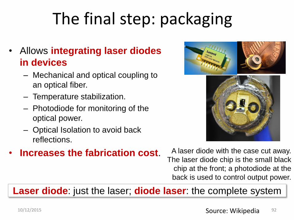
The final step: packaging
• Allows integrating laser diodes
in devices
– Mechanical and optical coupling to
an optical fiber.
– Temperature stabilization.
– Photodiode for monitoring of the
optical power.
– Optical Isolation to avoid back
reflections.
• Increases the fabrication cost.
10/12/2015 92
A laser diode with the case cut away.
The laser diode chip is the small black
chip at the front; a photodiode at the
back is used to control output power.
Source: Wikipedia
Laser diode: just the laser; diode laser: the complete system
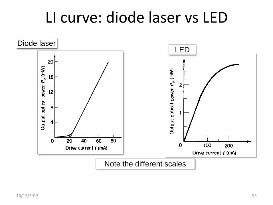
LI curve: diode laser vs LED
10/12/2015 93
Diode laser LED
Note the different scales

Power conversion efficiency (PCE)
10/12/2015 94
• Is the slope of the LI curve,
PCE =ΔP0/ΔI
• Typically 50% at 50 C.
• Other efficiency measures:
─ quantum efficiency
─ overall efficiency
LI curve
Thermal effects at high currents
lead to saturation (more latter)

Quantum efficiency • Laser optical power: P= h (in Watts)
: flux of emitted photons (photons per unit time).
• = d (I-Ith)/e (I, Ith in amperes)
d : quantum efficiency. It accounts for the fact that only a
fraction of the electron-hole recombinations are radiative
(internal efficiency) + only part of the emitted photons are
useful (emission efficiency)
P = h d (I-Ith)/e =1.24 d (I-Ith)/
10/12/2015 95
Example:
• Ith= 21 mA
• =1.3 m (InGaAsP)
• d =( /1.24) P/(I-Ith)=0.4

Overall efficiency
• Ratio of optical power to electrical power, = P/IV
• P = (h/e) d (I-Ith)
• V = Vk + RdI
Vk is the kink voltage (related to the separation of quasi-
Fermi energies)
Rd = dV/dI is the differential resistance
• = (h/e) d (I-Ith) /I(Vk + RdI)
• is a function of the injected current, I
• The efficiency is maximum when
10/12/2015 96
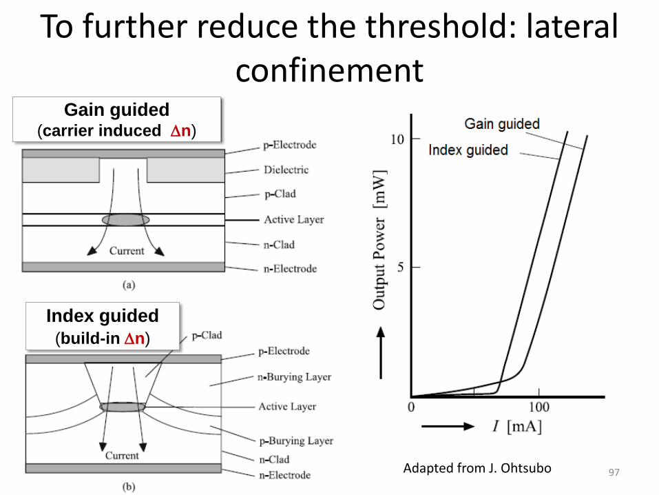
To further reduce the threshold: lateral confinement
10/12/2015 97 Adapted from J. Ohtsubo
Gain guided (carrier induced n)
Index guided
(build-in n)
10/12/2015 98 Source: J. Bowers (UCSB)

Emission characteristics: how many modes?
10/12/2015 99
(free-space wavelength
spacing, measured with an
Optical Spectrum Analyzer)
n = 3.5, L = 1 mm:
Δλ = 0.05 nm @ 635 nm
Δλ = 0.3 nm @ 1550 nm
Δ = c/(2nL)
Δλ = (λo)2/(2nL)
m = m (c/n)/(2L)
(mirrors)
• The semiconductor gain spectrum is broad
supports many longitudinal modes.

Exercise
10/12/2015 100
Consider a InGaAsP (n=3.5) laser with a FP cavity of length
L = 400 m. If the gain spectral width is 1.2 THz, how many
longitudinal modes may oscillate? If the central wavelength is
1.3 m, which is the wavelength spacing?
Δ = c/(2nL) Δλ = (λo)2/(2nL)

10/12/2015 101
Gain + cavity determine the optical spectrum
• The number of lasing
modes and their
relative power depends
on gain (current and
temperature) and on
the type of laser.
• It is often possible to
adjust I and T for
single-mode operation,
but it can be achieved
over a limited I and T
range.

Thermal properties: variation of the emission wavelength
10/12/2015 102
Multimode: Mode hopping Single-mode laser
0.4 nm/C

Thermal effects in the LI curve
10/12/2015 103
Thermal variation of threshold current
Thermal
saturation

Why thermal variations?
10/12/2015 104
With increasing current, increasing temperature (Joule
heating).
Temperature affects:
• the gain (the peak and the width)
• the refractive index
Kramers-Kronig: gain ─ Im(), n Re()
The temperature modifies the refractive index which in
turn modifies the cavity resonance.

Outline: semiconductor lasers
• Fabrication
• LI curve (efficiency, threshold)
• Characteristics (optical spectrum, thermal effects)
• Types of semiconductor lasers
– Single mode -- multimode
– Edge emitting and vertical cavity
– Semiconductor but not diode lasers • Quantum cascade lasers
• Optically pumped semiconductor lasers
• New materials and cavity designs
10/12/2015 105

Can we fabricate single-mode lasers?
• Single-mode emission is important for optical fiber
communications and for applications that require high
beam quality.
• Dynamically stable single-mode emission can be achieved
by using a mode-selective cavity:
– An external mirror – External Cavity Laser (ECL)
– A Bragg-Grating (BG) mirror
• Distributed Feedback (DFB)
• Distributed Bragg Reflector (DBR)
• Vertical Cavity Surface Emitting Lasers (VCSEL)
10/12/2015 106

External Cavity Laser
10/12/2015 107
• With controlled feedback conditions the laser emission
“locks” to one of the modes of the “compound” cavity.
Advantage: decrease of the threshold current (reduced
cavity loss) and reduced line-width.
• Drawback: uncontrolled feedback conditions can lead to
instabilities and chaotic emission (more latter).

Bragg-Grating (BG) devices
10/12/2015 108
DBR
(1972)
DFB
• Peak reflectivity for a specific frequency (the Bragg-frequency)
via coherent addition of distributed reflections.
VCSEL
(mid 1980s)

Optical spectra
10/12/2015 109

EEL vs VCSEL
L 300-500 m
The semiconductor
facets serve as mirrors
Two DBRs serve as mirrors
L=1-10 m
Edge-Emitting Laser (EEL)
VCSEL
Wide divergent output
Δλ = (λo)2/(2nL)
EELs and VCSELs have very different cavity lengths and mirror
reflectivities (30%, 99%), but similar photon lifetimes.
single-longitudinal-mode.
L

Exercise
10/12/2015 111
InGaAsP (n=3.5) VCSEL laser with L = 5 m. If the gain
spectral width is 1.2 THz, how many longitudinal modes may
oscillate? If the DBRs reflectivity is 99%, what is the photon
lifetime? Compare with an EEL of L = 400 m.
= 8.5 THz, 1 mode Δ = c/(2nL)
p=n/(cr) r=i-ln(R1R2)/2L r= Distributed loss coefficient
p-(2nL/c)/ln(R1R2) p=3.5 – 6 ps
R1=r12, R2=r2
2

VCSEL advantages
• Single-longitudinal-mode
• Low threshold currents & high efficiency
• Circular beam profiles with small divergence angles, simplifying the
design of beam-shaping optics.
• High data transmission speed (850 nm, 40 Gbit/s up to 80 C –Sep. 2014).
• The active diameter of the VCSEL can be reduced to just a few μms in
order to obtain single-transverse-mode operation together with lowest
threshold currents in the sub-100 μA range.
• It can also exceed 100 μm to get high output powers beyond 100 mW.
• Device testing at the wafer level: low fabrication cost.
• Straightforward fabrication of homogeneous 1D and 2D laser arrays.
Any drawbacks? Yes! Polarization instability, thermal sensitivity & multiple
transverse modes (broad-area devices)
112

10/12/2015 113

Scalability
10/12/2015 114
Chip with an array of
thousands of
VCSELs
Building blocks of increasing power and size.
Submodule with 12 x 14
chips on sub-mounts on
a micro-channel cooler
System of 3.5 kW
consisting of 24
sub-modules.
Kolb et al 2013

10/12/2015 115
Lateral/transverse modes
Edge-Emitting Lasers: VCSELs:
• The circular
profile allows
easy coupling to
an optical fiber.
• But single-
transverse mode
emission limited
to few mW.
Solutions of the
Helmholz equation
Adapted from A. Larsson, JSTQE 2011
Fundamental mode operation can be achieved by
matching the mode area to the active gain area.

Complex transverse patterns
10/12/2015 116
Near-field intensity distributions at different injection currents (9 mA 15
mA 20 mA and 25 mA).
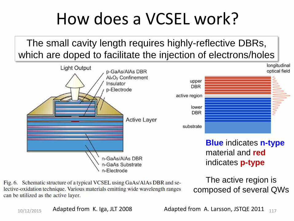
How does a VCSEL work?
10/12/2015 117 Adapted from K. Iga, JLT 2008
Blue indicates n-type
material and red
indicates p-type
Adapted from A. Larsson, JSTQE 2011
The small cavity length requires highly-reflective DBRs,
which are doped to facilitate the injection of electrons/holes
The active region is
composed of several QWs

VCSEL design
10/12/2015 118
• DBRs: typically 30 layer
pairs.
• QWs: typically 10-15
distributed over few λs.
Adapted from M. Dawson
• Because of thermal effects, VCSELs are engineered with a
‘gain offset’.

Long wavelength VCSELs: DBRs drawbacks
• GaAs-based devices benefit from a large index difference
between GaAs and AlAs that allows to fabricate high-
reflective DBRs even with small numbers of layers.
• But long-wavelength VCSELs based on InP suffer from
almost a factor of two smaller index contrast of the
InGaAsP or InGaAlAs mirror layers. Thus, larger numbers
of layer pairs are required for good mirror reflectivity.
• Also a problem: larger layer thicknesses (due to the longer
wavelength), the epitaxial mirror stacks of the InP-based
VCSELs become rather thick.
• Also a problem: heating due to the high thermal resistance
of DBRs.
10/12/2015 119
Current confinement
Mesa etching (air-post)
Drawback: scattering
losses of the optical
field and reliability
problems if the active
region is exposed to air.
10/12/2015 120
Selective oxidation
introduces less
optical losses in the
cavity and improves
performance
Ion implantation
(predominantly
using protons)
creates highly
resistive
semiconductor
regions

Comparison
10/12/2015 121 Adapted from J. Hecht

A limit for the wavelength of semiconductor lasers
• In conventional semiconductor lasers, when electrons
from the conduction band relax to the valence band, the
energy is typically transferred to a photon.
• At longer wavelengths, depending on the band structure
and temperature, this energy is often re-absorbed by
another charge carrier and eventually transferred to heat.
• Thus, the emission wavelength of conventional, inter-
band lasers is limited to about 3 m.
• Solution: inter-sub-band transitions.
10/12/2015 122

10/12/2015 123
CW RT emission achieved in 2002

10/12/2015 124
• No recombination!
• QCL: semiconductor
laser but not diode
laser.
• Electrons flow through
series of quantum wells
• Emitting a photon each
time.
• One electron generates
many photons
sequentially.
Adapted from J. Faist
QCLs operating principle
• Quantum well determines
wavelength
• Wavelengths ~3 μm to THz

10/12/2015 125
Optics and Photonics News, July/August 2008
QCLs applications

Optically pumped semiconductor (OPS) laser (also known as VECSEL)
• Uses GaAs & other
III-Vs
• Bragg reflector on
bottom of device
• External cavity (0.1
mm – few 10’s cm)
• Output coupler
separate
• Tunable (15-180 nm)
• Wavelengths: 670 nm
to 2.2 μm
10/12/2015 126 Adapted from M. Dawson

Summarizing, the design goals of semiconductor light sources are
To optimize carrier injection properties
To optimize optical confinement
To minimize optical loss and heating
To obtain maximum gain at a given injection power
To obtain high-quality spatial profile and spectral purity
To cover a wide range of wavelengths
10/12/2015 127

• Fabrication
• LI curve (efficiency, threshold)
• Characteristics (optical spectrum, thermal effects)
• Types of semiconductor lasers
• New materials and cavity designs
10/12/2015 128
Outline: semiconductor lasers

10/12/2015 129
Ring cavity: whispering-gallery modes
• Discovered
by Raman in
1920 while
visiting
London
Cathedral.
Source: OPN July 2013

10/12/2015 130
Source: Sorel et al, JQE 2003
Microdisk (“ring”) laser Two “whispering-gallery” modes
A thin disk of semiconductor
material in which whispering-
gallery modes circulate around
the edge of the disk.

10/12/2015 131
• Like a whispering gallery mode, the light
propagates around the edges of the
pillars, but in a helix rather than a circle.
• Although light propagating downward is
absorbed by the substrate, enough gain
in the upward propagating allows lasing.
• The semiconductor cavity mode alone
provides enough confinement (no need
of metal cavity).
• Sub-wavelength lasing: the pillars are
smaller on a side than the wavelength
they emit.
See also OPN May 2011

10/12/2015 132
Optically pumped by using a mode-locked Ti:sapphire laser

Nanolasers
• Have dimensions or modes sizes close to or smaller
than the wavelength of emitted light.
• Developed thanks to innovative use of new materials
and cavity designs.
– dielectric lasers,
– metallic and plasmonic lasers,
– small bio-compatible or bio-derived lasers
10/12/2015 133

Exciton–polariton lasers
• No population inversion.
• Exciton–polariton condensation in microcavities represents a
fundamentally different and potentially more efficient process for
generating coherent light.
• Exitons-polaritons: quasiparticles formed in resonators that provide
strong coupling between intracavity photons and the excitonic states of
a gain medium inside the resonator.
• (Reminder: an exciton is a e/h pair held together by their Coulomb
attraction).
• In the strong coupling regime, exciton–polaritons can form a condensate
if their density is sufficiently high.
• Photon leakage from a resonator containing such a condensate yields
coherent light that is nearly indistinguishable from conventional laser
emission.
10/12/2015 134

Exciton–polariton laser: how does it work?
• Strong coupling can be achieved by locating the gain
medium at the antinodes of the cavity photon mode
(same as in VCSELs).
• Polariton lasing was achieved by repopulating the
condensate through optical pumping [Kasprzak, J. et al.
Nature 443, 409–414 (2006).].
• Electrically pumped polariton lasing has also been
demonstrated, although only at cryogenic temperatures
and under substantial magnetic fields [Schneider, C. et
al. Nature 497, 348–352 (2013).].
10/12/2015 135

o
10/12/2015 136

Fundamental challenges involved in laser miniaturization
10/12/2015 137
The shortest L is 0/2 (m = 1)
Phase condition
Amplitude condition region active volume
mode optical volume
The gain limit is often the greatest constraint on L, as the cavity must be long enough to compensate for the mirror losses.

Limit in the transverse direction
10/12/2015 138
For lasers based on dielectric
waveguides, reducing the
thickness d of the waveguide
leads to substantial broadening
of the transverse field.
Metallic waveguides allow
reduced transverse dimensions
and a subwavelength localized
transverse field, at the cost of
increased loss due to absorption
in the metal
Reducing a laser’s transverse dimensions involves a trade-off between confinement and losses

State-of-the-art: laser size (Dec. 2014)
10/12/2015 139
- open symbols: volume - filled symbols: dimension
• Dielectric cavities: diamonds, VCSELs; squares, microdisk; circles,
photonic crystal.
• Metal cavities: upwards triangles, metallic non-plasmon mode;
downwards triangles, metallic plasmon mode.

State-of-the-art: laser threshold (Dec. 2014)
10/12/2015 140
Threshold in W (optical pumping) and in A (electrical pumping,)
• Dielectric cavities: diamonds, VCSELs; squares, microdisk; circles,
photonic crystal.
• Metal cavities: upwards triangles, metallic non-plasmon mode; downwards
triangles, metallic plasmon mode.
- Open symbols:
cryogenic
temperatures;
- filled symbols:
RT.

Active materials for small lasers
• Conventional semiconductors are the widely used because:
– they allow direct electrical pumping and
– they provide high optical gain. Specially QDs, however, there is the
drawback of limited overlap of the optical mode with the small QDs.
• Main drawback of conventional semiconductors: tunability.
Tunable lasers usually require complex fabrication processes.
• Alternative materials: organic dyes, organic semiconductors
and colloidal quantum dot nanocrystals. They can be prepared
as thin films (thicknesses <<1 μm) by solution-based
processes.
• They gain spectrum can be tuned by targeted modifications of
chemical structure, composition and characteristic dimension.
10/12/2015 141
Alternative materials
Organic semiconductors
• Hydrocarbon-based compounds with strong optical transitions and
electronic semiconducting properties.
• Low charge-carrier mobility has so far prevented lasing through direct
electrical pumping.
Fluidic lasers
• Organic dye solutions have historically been used in macroscopic,
wavelength-tunable dye-lasers operating at visible and near-infrared.
• Microfluidics has enabled the application of such solutions in small
lasers (fluidic lasers)
• In fluidic lasers the refractive index and gain spectrum of the active
medium are tunable by exchanging the solvent or dye passed through
the device.
10/12/2015 142

Tunability
10/12/2015 143
Photoluminescence (PL) and
electroluminescence (EL) spectra
from five different types of colloidal
quantum dots, spanning the entire
visible spectrum.
Emission wavelength of organic-
semiconductor-based distributed
feedback lasers, tuned by adjusting
the thickness of the gain layer.

Optical gain materials used in small lasers
10/12/2015 144
Squares: electrical
pumping;
Circles: amplified
spontaneous
emission (ASE)
with nanosecond
optical pumping;
Triangles: ASE
subpicosecond
optical excitation;
open symbols:
gain achieved at
cryogenic
temperatures
broad
emission
and gain
spectra
that can be
tuned by
chemical
modificatio
n or size
variation

Single-cell biological lasers
• A single biological cell can form a
small laser if genetically programmed
to produce green fluorescent protein
(GFP). Schematic of the first single-
cell laser (left) and typical spatial
emission pattern (right)
10/12/2015 145
Gather and Yun, Nat. Phot. 2011
A single-mode distributed feedback laser made from gelatine doped with
riboflavin (vitamin B2); both materials are nontoxic and digestible. The
researchers obtained lasing at wavelengths of 543 nm and 562 nm.

In the other extreme of cavity sizes Fiber lasers
• Gain medium: optical fiber, doped with rare-earth ions (Erbium-doped
is one of the most common).
• Why erbium?
• Erbium atoms have very useful energy levels: there is one that can
absorb 980 nm photons, and decays to a meta-stable state at 1550nm.
10/12/2015 146
Km long cavity, millions of longitudinal modes
Main advantage: portability. The delivery of the beam does not require
any sensitive optics.

TF test In EELs the Fabry-Perot cavity is formed by the cleaved facets of
the semiconductor material.
EELs and VCSELs have active regions of comparable sizes.
Bragg-Grating lasers (DFBs and DBRs) emit a multimode
spectrum.
The goal of diode laser design is to improve the confinement of
photons and carriers, which allows lowering the threshold current.
The threshold of diode lasers and amplifiers is at transparency,
when the rate of stimulated emission is equal to absorption.
Thermal heating is responsible for the saturation of the LI curve and
the shift of the emission wavelength with increasing current.
Bulk lasers are as efficient as QW lasers.
Quantum cascade lasers operate on inter-sub-band transitions.
10/12/2015 147
THANK YOU FOR YOUR ATTENTION !
Universitat Politecnica de Catalunya
http://www.fisica.edu.uy/~cris/