Embed Size (px)
Citation preview
LASER PROCESSING OF METALS AND POLYMERS
by
Senthilraja Singaravelu B.Sc., May 1998, University of Madras, India M.Sc., May 2001, Bharathiar University, India
M.S., May 2006, Old Dominion University, USA
A Thesis Submitted to the Faculty of Old Dominion University in Partial Fulfillment of the
Requirements for the Degree of
DOCTOR OF PHILOSOPHY
PHYSICS
OLD DOMINION UNIVERSITY May 2012
Approved by:
________________________ Geoffrey A. Krafft (Director)
________________________ Michael J. Kelley
________________________ Gail E. Dodge ________________________ Charles I. Sukenik ________________________ Patrick G. Hatcher
ABSTRACT
LASER PROCESSING OF METALS AND POLYMERS
Senthilraja Singaravelu Old Dominion University, 2012
Co-Directors: Dr. Michael J. Kelley Dr. Geoffrey A. Krafft
A laser offers a unique set of opportunities for precise delivery of high quality
coherent energy. This energy can be tailored to alter the properties of material allowing a
very flexible adjustment of the interaction that can lead to melting, vaporization, or just
surface modification. Nowadays laser systems can be found in nearly all branches of
research and industry for numerous applications. Sufficient evidence exists in the
literature to suggest that further advancements in the field of laser material processing
will rely significantly on the development of new process schemes. As a result they can
be applied in various applications starting from fundamental research on systems,
materials and processes performed on a scientific and technical basis for the industrial
needs. The interaction of intense laser radiation with solid surfaces has extensively been
studied for many years, in part, for development of possible applications. In this thesis,
I present several applications of laser processing of metals and polymers including
polishing niobium surface, producing a superconducting phase niobium nitride and
depositing thin films of niobium nitride and organic material (cyclic olefin copolymer).
The treated materials were examined by scanning electron microscopy (SEM),
electron probe microanalysis (EPMA), atomic force microscopy (AFM), high resolution

optical microscopy, surface profilometry, Fourier transform infrared spectroscopy (FTIR)
and x-ray diffraction (XRD). Power spectral density (PSD) spectra computed from AFM
data gives further insight into the effect of laser melting on the topography of the treated
niobium.

iv
This thesis is dedicated to my parents, sister and all my teachers.

v
ACKNOWLEDGMENTS
My Ph. D. degree would not have been possible, without the guidance and the help of several individuals, who in one way or another, contributed and extended their valuable assistance and support, in the preparation and completion of this study. It is my pleasure to thank those who helped me accomplish my desire.
I am whole heartedly grateful to my Ph.D advisors Dr. Michael J. Kelley and Dr. Geoffrey Krafft. Thanks to Dr. Michael J. Kelley for planning my research, training me and guiding me in each step of research. Thanks for the enthusiasm, inspiration, and great efforts to explain things clearly and constant encouragement to complete my assignment. Their guidance and support from the initial to final stage enabled me to develop an understanding of the subject. Thanks to Dr. Geoffrey Krafft for accepting me as his student and guiding me throughout the journey of Ph.D. Thank you for all the support you both have provided me, if not I would have been lost.
I would like to thank my committee members (Dr. Gail Dodge, Dr. Charles Sukenik and Dr. Patrick Hatcher) for their patience, guidance and contributions to my thesis. A special thanks to our department chair Dr. Charles Sukenik and Dr. Gail Dodge who were always ready to help me professionally and personally. I would like to thank Dr. Lepsha Vuskovic for her understanding and support. I also thank the funding support I have received without it this research would not have been possible.
It was a privilege to be trained by a group of scientists, who are the core of FEL family. Working with different teams like FEL, SRF, and CASA has given confidence and inspiration for my future life. Thank you all.
I owe my deepest gratitude to Dr. J. Michael Klopf from FEL team, who was beside me supporting my experiments. Any discussion I had with him has always been informative and helpful. Thanks for his encouragement and patience. He faced the challenge of a demanding student as I was. Eventually my progress will inspire many more research students to seek his fortunate advice and guidance.
I wish to thank Dr. Shukui Zhang from FEL team for training and teaching me the laser system. I can never forget the timely help rendered by Dr. Gwyn Williams, Dr. Steve Benson, Dr. Jim Coleman, Cody Dickover, Chris Gould, Joe Gubeli, Kevin Jordan, Jim Kortze, Dan Sexton, Dr. Michelle Shinn, Dr. Richard Walker, Tom Powers and Guy Wilson, during my stay in FEL building by providing all the help I requested for.
I was greatly benefited working with Dr. Whelan Colm, Dr. Mark Havey and
vi
Dr. Moskov Amaryan while I was their student during the first few years of my Ph.D life. Thank you very much. I would also thank Dr. Areti Hari for all advice and help that made my paper work along with the funds easy.
With deep love and respect, I would like to thank Dr. Richard Haglund (VU), Dr. Ken Schriver (VU), Dr. Sergey Avanesyan (VU), and Dr. Hee Park (AppliFlex LLC) for helping me in doing the entire polymer experiments and giving me a wonderful chance to work at the Vanderbilt University campus. My stay on the campus during the experiment made me feel at home. I thank all of them for their constant support and concern for me.
Thanks to Prof. Dr. P. Schaaf (Germany) for graciously providing the basic simulation codes from which the thermal simulation model was developed for our experiment.
Thanks to Walt Hooks and Vicky (RIP) for keeping their affectionate homes and hearts open for me from the day I entered the USA. Thanks to the wonderful department staff Annette Vialet, Delicia Malin, Gabriel Franke and Lisa Okun for their help and support over the years. I can never forget the timely help they rendered. The help they provided to select the warm clothes can never be forgotten. I would also like to thank Dr. Ravi Mukamala (ODU) & family for considering me as one of their sons and keeping their doors open for me always.
I am grateful to Dr. Desmond Cook (ODU), H. W. Stephen (ODU), A. Wilkerson (W&M), B. Robertson (W&M), O. Trofimova (W&M) and N. Moore (W&M) for training me and also permitting me to use different equipments in their lab to characterize my samples. Thanks to Dr. D.M. Bubb (RU), Dr. A.J. Glover (W&M) and Dr. D. Kranbuehl (W&M) for helping me to take the thermal dependent parameters for organic material.
It is my pleasure to thank my high school teachers (Mrs. Maragadavalli and Mr. Anbalagan), Undergraduate professors (Prof. Eshwaran and Dr. T.K. Vasudevan), post-graduate professors (Prof. M. Seethuraman, Prof. K. Subramaninan, Dr. V.Selvarajan, Dr. Sa. K. Narayanadass and Dr. R.T. Rajendra Kumar) who not only taught me the subject but also showed me the path to success. Thank you very much.
I am immensely grateful to my spiritual Guru (teacher) Dr. Gopalan (India) from whom I learned meditation, yoga and the proper way to see GOD and seek peace and blessings.
I am indebted to my elders and friends (V. Shesadri, Dr. Bhavaneswari, Dr. Saradhadevi, Nachimuthu, Sivabalamurugan, Dr. Raghupathi and Valapadi Senthil)
vii
for providing a stimulating and fun loving environment to learn and grow. This was the group from whom I developed self confidence.
I wish to express my deepest gratitude to Dr. M.K. Shobana (Korea) and Dr. K.P. Sreekumar Nair (BARC, India), who morally supported me, encouraged me, and wished me much success in reaching my goals. I also want to take this chance to thank Govindarajan (India), Uma Shankar (India), P. Venkatesh (India), G. S. Thirugnanasambanthan (India), Dr. B. Janarthanan (India), Dr. A. Kovalan (India), Dr. Hiran Kumar (India), Lavanya Krishnan and V. Govindarajan (India) who stood beside me, while I was in need of some good moral support. Thank you all.
I wish to thank all my friends from ODU, Asma Begum (Bangladesh) & family, Kurnia & family, P. Donika, K. Omkar, S.U. DeSilva, A. L. Win, P. Srujana, K. Raghavendra, Vinutha Nakul, M.N. Hazhir Rashad, Vinutha Nakul, C. Chellam, G. Randika, and T. Rajintha for having very good moment in life, especially S. G. Nandakarthik, U. Janardan, R. Nakul, and Sathish Sathiyanesan for standing beside me through all the difficult times. Thank you all for all the emotional support, camaraderie, entertainment and the friendly care I received. There are so many other ODU friends and ISA-ODU, I am proud to have known. I am extremely thankful to other friends and well wishers not mentioned here, who have encouraged and helped me to reach this level.
I would like to take this opportunity to thank Soubeika Bahri (CUNY) for all the support she has provided during the last few years of my Ph.D life.
Last and most important, I wish to thank my parents Mr. K. Singaravelu and Mrs. S. Malliga, who gave me a good start in life by nourishing me mentally, physically, and spiritually. Their constant support, blessings and prayers strengthened me. I am grateful for their patience for the long separation caused by my living in the USA. Thank you very much. I would like to thank my sister Dr. Malarvizhi Thirukumarn for all the support she has given me, for which these pages are not enough. With deep love and respect, I would like to thank the entire extended family and my supportive brother-in-law Dr. Thirukumaran and my cute–charming nephew Narain karthikeyan. I would also like thank Sabitha Rani & their family members for staying beside my parents while I was away from them.
All of these people and entities were instrumental in one way or another in achieving the goal that I set out to accomplish. From the depth of my heart I thank you all for your precious time you spent with me and also for bearing with me and believing in me. I am extremely thankful to the Omnipotent and Omnipresent Almighty, who has always kept me in the hollow of His hand and who had placed me amidst a caring, dedicated and knowledgeable core group of teachers, guides, colleagues, family members and friends.
viii
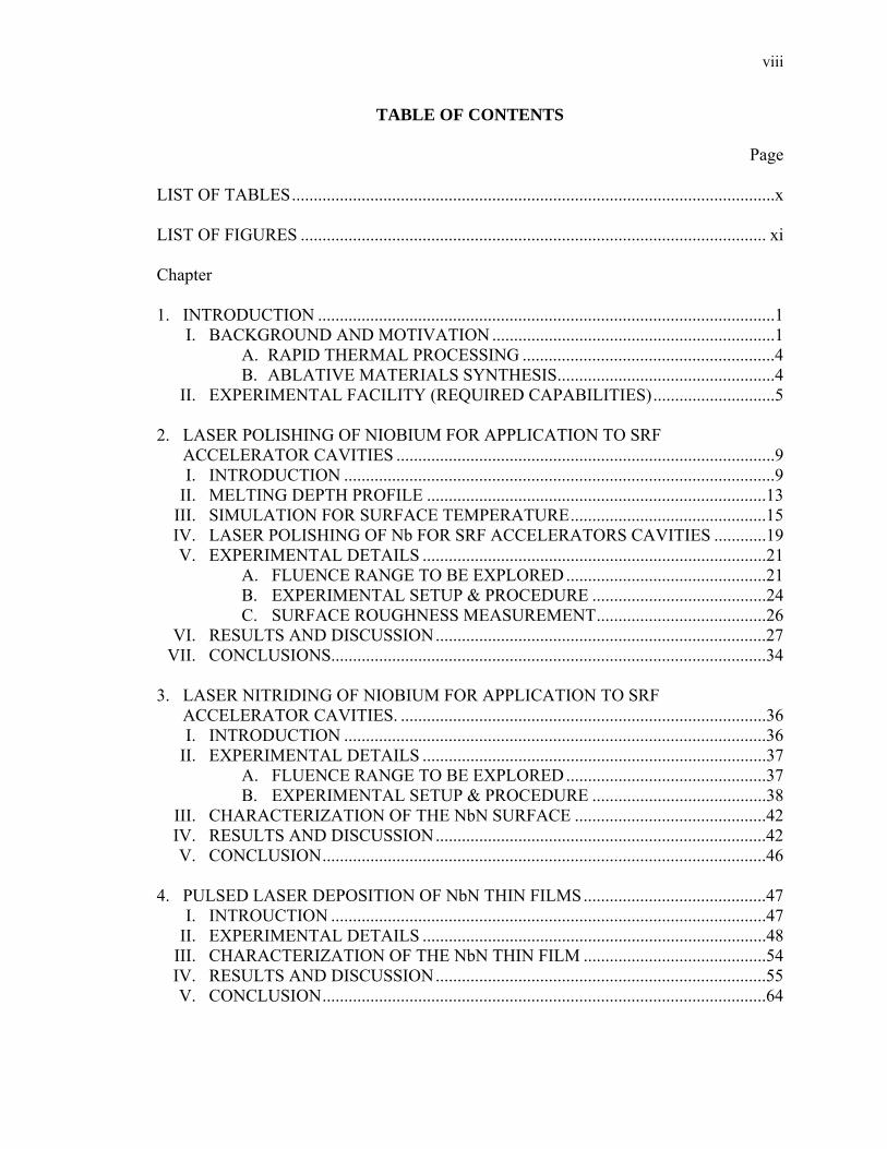
TABLE OF CONTENTS
Page LIST OF TABLES ...............................................................................................................x LIST OF FIGURES ........................................................................................................... xi Chapter 1. INTRODUCTION .........................................................................................................1
I. BACKGROUND AND MOTIVATION .................................................................1 A. RAPID THERMAL PROCESSING ..........................................................4 B. ABLATIVE MATERIALS SYNTHESIS ..................................................4
II. EXPERIMENTAL FACILITY (REQUIRED CAPABILITIES) ............................5 2. LASER POLISHING OF NIOBIUM FOR APPLICATION TO SRF
ACCELERATOR CAVITIES .......................................................................................9 I. INTRODUCTION ...................................................................................................9
II. MELTING DEPTH PROFILE ..............................................................................13 III. SIMULATION FOR SURFACE TEMPERATURE .............................................15 IV. LASER POLISHING OF Nb FOR SRF ACCELERATORS CAVITIES ............19 V. EXPERIMENTAL DETAILS ...............................................................................21
A. FLUENCE RANGE TO BE EXPLORED ..............................................21 B. EXPERIMENTAL SETUP & PROCEDURE ........................................24 C. SURFACE ROUGHNESS MEASUREMENT .......................................26
VI. RESULTS AND DISCUSSION ............................................................................27 VII. CONCLUSIONS....................................................................................................34
3. LASER NITRIDING OF NIOBIUM FOR APPLICATION TO SRF
ACCELERATOR CAVITIES. ....................................................................................36 I. INTRODUCTION .................................................................................................36
II. EXPERIMENTAL DETAILS ...............................................................................37 A. FLUENCE RANGE TO BE EXPLORED ..............................................37 B. EXPERIMENTAL SETUP & PROCEDURE ........................................38
III. CHARACTERIZATION OF THE NbN SURFACE ............................................42 IV. RESULTS AND DISCUSSION ............................................................................42 V. CONCLUSION ......................................................................................................46
4. PULSED LASER DEPOSITION OF NbN THIN FILMS ..........................................47
I. INTROUCTION ....................................................................................................47 II. EXPERIMENTAL DETAILS ...............................................................................48
III. CHARACTERIZATION OF THE NbN THIN FILM ..........................................54 IV. RESULTS AND DISCUSSION ............................................................................55 V. CONCLUSION ......................................................................................................64
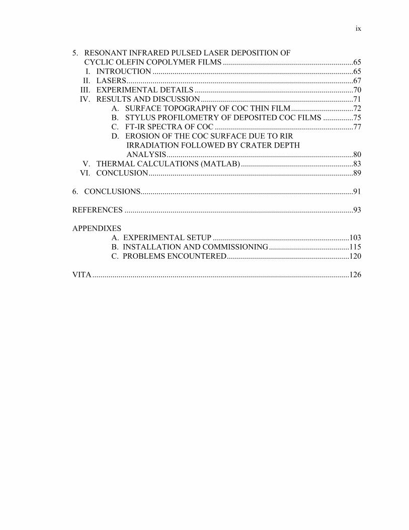
ix
5. RESONANT INFRARED PULSED LASER DEPOSITION OF CYCLIC OLEFIN COPOLYMER FILMS .................................................................65 I. INTROUCTION ....................................................................................................65
II. LASERS .................................................................................................................67 III. EXPERIMENTAL DETAILS ...............................................................................70 IV. RESULTS AND DISCUSSION ............................................................................71
A. SURFACE TOPOGRAPHY OF COC THIN FILM ...............................72 B. STYLUS PROFILOMETRY OF DEPOSITED COC FILMS ...............75 C. FT-IR SPECTRA OF COC .....................................................................77 D. EROSION OF THE COC SURFACE DUE TO RIR
IRRADIATION FOLLOWED BY CRATER DEPTH ANALYSIS .............................................................................................80
V. THERMAL CALCULATIONS (MATLAB) ........................................................83 VI. CONCLUSION ......................................................................................................89
6. CONCLUSIONS..........................................................................................................91 REFERENCES ..................................................................................................................93 APPENDIXES A. EXPERIMENTAL SETUP ....................................................................103 B. INSTALLATION AND COMMISSIONING ........................................115 C. PROBLEMS ENCOUNTERED .............................................................120 VITA ................................................................................................................................126
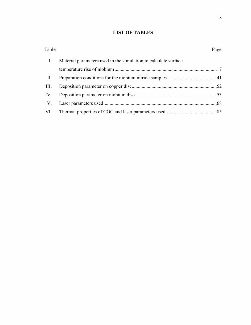
x
LIST OF TABLES
Table Page
I. Material parameters used in the simulation to calculate surface
temperature rise of niobium ...................................................................................17
II. Preparation conditions for the niobium nitride samples ........................................41
III. Deposition parameter on copper disc .....................................................................52
IV. Deposition parameter on niobium disc. .................................................................53
V. Laser parameters used ............................................................................................68
VI. Thermal properties of COC and laser parameters used. ........................................85

xi
LIST OF FIGURES Figure Page
1. Reflectivity of niobium at1064 nm as a function of incidence angle ....................12
2. Surface temperature as a function of time following a laser pulse
incident upon a surface ..........................................................................................14
3. Melting depth profile of a metal as a function of time ..........................................14
4. Thermal conductivity of niobium as a function of temperature ............................17
5. Absorption coefficient of niobium as a function of wavelength ............................18
6. Calculated time dependence of niobium surface temperature after
irradiation by a single 15 ns pulse of the indicated fluence ...................................18
7. Maximum surface temperature irradiated by a single 15 ns pulse of
various fluences .....................................................................................................19
8. Calculated peak surface temperature after a single laser pulse of the
fluence indicated for three initial temperatures .....................................................22
9. Calculated maximum melt depth after a single laser pulse of the fluence
indicated for three different initial temperatures ...................................................23
10. Calculated melt life time for a single laser pulse of the fluence indicated
for three different initial temperatures ...................................................................24
11. Untreated surface (before laser processing)
(a) SEM image (b) AFM image; 10 μm/div horizontal, 0.5 μm/div vertical ........28
12. AFM images of the niobium surface subjected to 75 pulses at the
indicated fluence ...................................................................................................29
13. Surface roughness after 75 laser pulses of the indicated fluence ...........................29
14. Increased surface roughness due to higher laser fluence treatment .......................30
15. Interface between the treated (1.1 J/cm2 16 kHz and ~75 pulses total per
area) and untreated niobium surface ......................................................................30
16. AFM image of niobium surface irradiated by the indicated number of
1.1 J/cm2 pulses ......................................................................................................31
17. Surface roughness after irradiation by the indicated number of pulses
at a fluence of 1.1 J/cm2 .........................................................................................32
xii
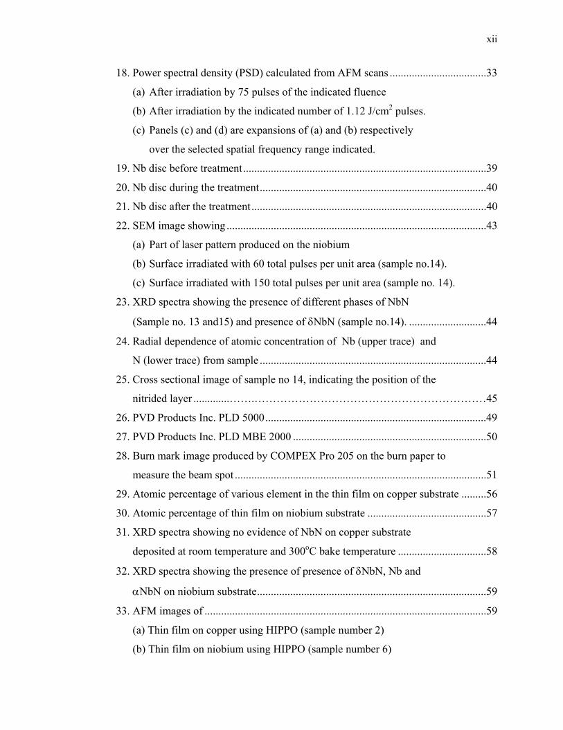
18. Power spectral density (PSD) calculated from AFM scans ...................................33
(a) After irradiation by 75 pulses of the indicated fluence
(b) After irradiation by the indicated number of 1.12 J/cm2 pulses.
(c) Panels (c) and (d) are expansions of (a) and (b) respectively
over the selected spatial frequency range indicated.
19. Nb disc before treatment ........................................................................................39
20. Nb disc during the treatment ..................................................................................40
21. Nb disc after the treatment .....................................................................................40
22. SEM image showing ..............................................................................................43
(a) Part of laser pattern produced on the niobium
(b) Surface irradiated with 60 total pulses per unit area (sample no.14).
(c) Surface irradiated with 150 total pulses per unit area (sample no. 14).
23. XRD spectra showing the presence of different phases of NbN
(Sample no. 13 and15) and presence of δNbN (sample no.14). ............................44
24. Radial dependence of atomic concentration of Nb (upper trace) and
N (lower trace) from sample ..................................................................................44
25. Cross sectional image of sample no 14, indicating the position of the
nitrided layer .............…….………………………………………………………45
26. PVD Products Inc. PLD 5000 ................................................................................49
27. PVD Products Inc. PLD MBE 2000 ......................................................................50
28. Burn mark image produced by COMPEX Pro 205 on the burn paper to
measure the beam spot ...........................................................................................51
29. Atomic percentage of various element in the thin film on copper substrate .........56
30. Atomic percentage of thin film on niobium substrate ...........................................57
31. XRD spectra showing no evidence of NbN on copper substrate
deposited at room temperature and 300oC bake temperature ................................58
32. XRD spectra showing the presence of presence of δNbN, Nb and
αNbN on niobium substrate ...................................................................................59
33. AFM images of ......................................................................................................59
(a) Thin film on copper using HIPPO (sample number 2)
(b) Thin film on niobium using HIPPO (sample number 6)
xiii
(c) NbN thin film on niobium using excimer laser. (sample number 15)
34. SEM images of .......................................................................................................60
(a) Thin film on copper using HIPPO (sample number 2)
(b) Thin film on niobium using HIPPO (sample number 6)
(c) NbN thin film on niobium using excimer laser. (sample number 15)
35. Thickness measurements through SP on ................................................................62
(a) Thin film on copper for 30 min (sample number 2)
(b) Thin film on niobium for 90 min (sample number 15)
(c) NbN thin film on niobium for 120 min (sample number 16)
36. AFM image showing the border of thin film and the niobium substrate
(sample number15) ................................................................................................63
37. Adhesion measurements with scotch tape on thin film on niobium substrate .......63
38. (a) Schematic layout of the free-electron laser at the Jefferson National
Accelerator Laboratory, showing the photocathode electron source and
injector,the superconducting RF linac, the recirculation and energy-recovery
arc, and the optical cavity and wiggler that generates the tunable infrared
laser radiation (b) pulse structure of the FEL beam ..............................................69
39. Chemical structure of the cyclic olefin copolymer ................................................70
40. Scanning electron micrographs of the samples deposited on NaCl plates
using (a) Jefferson lab free-electron laser (b) Nanosecond HIPPO laser ..............72
41. Atomic Force Microscopy of the samples deposited on the NaCl plates
using (a) Jefferson lab free-electron laser, (b) HIPPO laser ..................................73
42. Optical image of the target exposed with (a) FEL and (b) HIPPO laser ...............74
43. Stylus Profilometer of COC thin films deposited using (a) RIR ablation
and (b) far IR ablation laser ...................................................................................76
44. Measured FTIR spectra (a) comparing laser deposited thin films and bulk
COC target (b) expansion of FTIR spectra (c) measured FEL spectra during
deposition showing tuned peak at 3.41 μm and FWHM width of 75 nm ..............78
45. Surface changes on COC target due to various fluences produced by
the single FEL pulse ..............................................................................................81
46. Line scan obtained from Fig. 45 ............................................................................82
xiv
47. Single FEL pulse fluence vs deformation from flat surface ..................................83
48. Calculated laser induced temperature rise as a function of x and z in
COC using parameters as stated in Table VI .........................................................86
49. Specific heat and IR absorbance at 3.43 μm as a function of
temperature of COC .............................................................................................87
50. Surface temperature rise of the COC target at different fluence per pulse ............88
51. Maximum surface temperature vs fluence .............................................................89
1
CHAPTER 1
INTRODUCTION
I. BACKGROUND AND MOTIVATION
Invented in 1960, the laser offers a unique set of opportunities for precise delivery of
high-quality coherent energy. Due to stimulated emission in a resonator, the generated
photons are multiplied. As the stimulated photons share the same wavelength, direction,
and phase, the resulting electromagnetic wave is characterized by a high degree of
coherence, a very narrow spectral distribution, and low divergence. This unique behavior
results in very good focusing capabilities, and the resulting power densities in the focus
of a high-power laser can reach 1016 W/cm2 easily.1 Such high intensities enable (for
example) rapid thermal processing, where thermal energy is confined to the beam spot
without collateral damage to the adjacent material.
Sufficient evidence exists in the literature to suggest that further advancements in the
field of laser material processing will rely significantly on the development of new
process schemes. The process control system must enable the precise delivery of photons
to a specific material with high spatial and temporal resolution; i.e., the laser control
system parameters must be appropriately varied for the particular material under
irradiation at the optimum time.2 Prior experiments have demonstrated that a diverse set
of material transformations can be realized by a judicious choice of the common laser
process parameters, such as the wavelength, pulse amplitude, temporal and spatial
characteristics, polarization, and total photon dose.3-14
2
Considering the interaction of laser radiation with materials, there are a few key
parameters that come into play when predicting what effects take place. They are the
amount of average laser power delivered to the material interaction site when the laser is
operating in a continuous wave (CW) mode and the amount of laser energy in joules
delivered to the material interaction site when the laser is operating in a pulsed mode.
This energy and its spatial and temporal distribution determine what kind of material
modification will occur.15 To understand the effect of the laser beam on the irradiated
material, the electronic and lattice dynamics must be taken into account. In order to
induce any effect on the substrate, the laser light must be absorbed and the absorption
process can be thought of as an energy source inside the material.
The initial interaction during laser processing is the excitation of electrons (especially
in conductors), vibrations (in insulators), or both (in semiconductors) from their
equilibrium states to some excited state.16 These typical single photon processes are well-
known in a wide field of physics and have been discussed extensively.17, 18 The excitation
energy is rapidly converted into heat. This is followed by various heat transfer processes:
conduction into the materials, and convection and radiation from the surface. The most
significant heat transfer process is heat conduction into the material. The generation of
heat at the surface and its conduction in the material establishes the temperature
distribution in the material, and depends on its thermo-physical properties and the laser
parameters.
As mentioned above, in laser material processing the wavelength of the lasers and the
absorption spectrum of different materials is to be considered. For example, the
wavelength of CO2 lasers is 10.6 μm, which is highly reflective with copper. For that
3
reason, CO2 lasers are not typically used when doing material processing with copper.
Shorter wavelength lasers perform much better with copper. The wavelengths of other
lasers that are typically used for material processing are the Nd:YAG laser at 1.064 μm,
the Yb-fiber laser at 1.07 μm, the frequency doubled Nd:YAG at 0.532 μm, the excimer
laser that can provide at least four UV wavelengths including 0.244 μm, and recently the
tunable free electron lasers (FEL). When compared with conventional lasers, the
significant difference in the FEL lies with the laser medium, an energetic (free means
unbound) electron beam. Current FELs cover wavelengths from millimeter to the soft x-
ray range. The advantages of the FEL over conventional lasers include wavelength
tunability and high powers that can be achieved in areas of the infrared spectrum, which
have not been achieved using conventional lasers. The FEL’s unique tunability enables
the FEL to ablate organics with minimal chemical disruption.19,20
Nowadays laser systems can be found in nearly all branches of industry for numerous
applications. This is a result among other things of close interactions between the
industrial needs and fundamental research on systems, materials and processes performed
on a scientific and technical basis. Today, basic knowledge of the interactions between
laser radiation and materials exists, but not all phenomena are fully understood and some
of the process limits are not yet reached. Laser processing covers a wide range of power,
interaction time and process materials with length scales from nanometers to meters.
Therefore, developing a science base is challenging.21 Although often research is
application driven, basic understanding of the process often requires in depth knowledge
obtained through mathematical modeling of the process and online process diagnostics.
The understanding of the process limiting phenomena is a must in order to extend the
4
technical boundaries towards the physical limitations, so that laser materials processing
will become more and more economic.22 In summary, understanding the availability of
research equipment, laser resources and deposition technique to be used are the primary
steps to perform laser processing on both metals and polymers.
A. Rapid thermal processing
Materials processing is one of the important and active areas of research in heat
transfer today.23 Rapid thermal processing (RTP) of materials refers to manufacturing and
material fabrication techniques that are strongly dependent on the thermal transport
mechanisms, involving rapid heating and cooling processes.24 The laser pulse allows one
to restrict the energy deposition within the absorbing volume and minimize collateral
thermal damage.25 In RTP, the laser pulse duration (τp), is typically shorter than the time
of dissipation of the absorbed laser energy by the thermal conduction (τth), a condition
that is commonly referred to as thermal confinement.26, 27 The condition for thermal
confinement can be expressed as τp <τth ~ /DT, where DT is the thermal diffusivity of
irradiated material and Lp is the laser penetration depth or the size of the absorbing
structure. The pulse duration in this regime is usually shorter than the time needed for gas
phase bubble formation and diffusion in the process of heterogeneous boiling.28, 29 As a
result, the absorbing material can be overheated much beyond the boiling temperature,
turning a normal surface evaporation at low laser fluences into an explosive vaporization,
or phase explosion, at higher fluences.25-31
B. Ablative materials synthesis
The interaction of intense laser radiation with solid surfaces has been studied
extensively for many years as a result of possible applications, such as precision
5
machining, materials synthesis, thin film deposition, and laser induced breakdown
spectroscopy for elemental analysis of materials. An onset of massive material removal
or ablation is defined by the critical energy density sufficient for the overheating of the
surface layer up to the limit of its thermodynamic stability.25
The term ablation is generally used for material removal processes by photo-thermal
or photo-chemical interactions. In the photo-thermal process, the absorbed laser energy is
converted into thermal energy in the material. The subsequent temperature rise at the
surface may facilitate the material removal due to generation of thermal stresses. This
possibility is more pronounced in the inhomogeneous targets such as coated materials
where the thermal stresses cause the explosive ablation of thin films. When the incident
laser energy is sufficiently large, the temperature at the surface exceeds the boiling point
causing rapid vaporization. These processes of material removal by thermal stresses and
surface vaporization are generally referred to as thermal ablation.32
In conventional photo-ablation, the energy of the incident laser radiation causes the
direct bond breaking of the molecular chains in organic materials resulting in material
removal by molecular fragmentation. This suggests that for the ablation process, the
photon energy must be greater than the bond energy and that selection of wavelength is
more important for different organic materials, making the FEL a unique laser source for
photo-ablation of organic materials.
II. EXPERIMENTAL FACILITY
(REQUIRED CAPABILITIES)
To perform RTP, a chamber that can sustain both vacuum (~ 10-7 Torr) and positive
pressure (~ 600 Torr) is needed. Experiments conducted during positive pressure can be
6
used to nitride metals using RTP in a nitrogen atmosphere and the experiment conducted
in vacuum can be used to smooth (polish) the surface of the metals. A robust turbo pump
attached to the vacuum chamber would be useful to keep the vacuum stable throughout
the experiment. RTP does not require the use of external cooling agents. The high
thermal conductivity of metals causes rapid self-quenching which means that the laser
radiation heats up near surface layers only and the unmelted bulk material acts as the heat
sink.33 Motorized optics mounts and rotating target/substrate holders are needed, which
can control the laser beam path to raster on the metal surface according to some specific
pattern and velocity of beam rastering during the experiment. This laser rastering
procedure and target/substrate rotation velocity can also control the accumulated pulse
overlap per area on the surface of the samples.
Among different methods to deposit the thin films, pulsed laser deposition (PLD)34,35
is a physical vapor deposition (PVD) process that fulfills the needs. In PLD the materials
placed in a target are ablated by intense pulsed laser radiation in a vacuum or reactive or
inert processing gas atmosphere. There is an emerging body of results that indicate that
PLD may revolutionize the synthesis of complex inorganic and organic thin film
materials. A unique feature of PLD is that the source material is evaporated (ablated) in a
non equilibrium process such that material is evaporated at the stoichiometry of the bulk.
Hence, it is possible to prepare thin films of incongruently melting solids that have a
stoichiometry characteristic of the solid phase prior to melting. The ablation rates are
primarily determined by the laser fluence, the pulse duration, the number of pulses, and
the pulse repetition rates.
7
A PVD Products Inc. PLD 5000 system can sustain the pressure and vacuum needed.
This system is also capable of rastering the laser beam on the target to control
accumulated pulse overlap. Rastering the laser beam and individual rotation of target
pedestals provides an added advantage for laser processing.
For the present studies, a Spectra Physics, “High Intensity Peak Power Oscillator”
(HIPPO) nanosecond laser with 1064 nm wavelength is used. This laser can be used as
the source for RTP to nitride metals (here niobium), and also to ablate niobium from the
surface to produce a thin film. In contrast, tunable IR free electron lasers (FEL’s) have
faithfully deposited a wide range of organics. Such systems are too costly and too
complex to be widely deployed in the laboratories of individual investigators (Appendix
A provides details of the facility and more about PLD 5000 and laser systems used). So
the IR-FEL at Thomas Jefferson National Accelerator Facility was used to establish an
advanced PLD user facility based on the IR FEL in one of the labs of the FEL building, at
Jefferson Lab, in collaboration with the Laser Materials Interaction group at Vanderbilt
University and the Naval Research Laboratory. Appendix B provides shows several
pictures of the installation and commissioning of these systems in user lab of FEL
building.
Having the basics of laser-material interaction, the availability of the PLD 5000
system, the HIPPO ns laser, the FEL beam from Jefferson lab and space in FEL building
and other facilities like nitrogen gas, chiller water, etc, the installation and
commissioning of the equipment is documented as well as the experiments that were
finally performed. In this thesis, I present several applications of laser processing of
metals and polymers including polishing niobium surface (Chapter 2), producing a

8
superconducting phase niobium nitride (Chapter 3) and depositing thin films of niobium
nitride (Chapter 4) and cyclic olefin copolymer (Chapter 5).
9
CHAPTER 2
LASER POLISHING OF NIOBIUM FOR
APPLICATION TO SRF
ACCELERATOR CAVITIES
I. INTRODUCTION
Whenever the electromagnetic radiation hits the surface of any material or metal
various phenomena like reflection, refraction, absorption, scattering and transmission
occur. The total energy absorbed is an important parameter in laser material interactions.
Absorption of radiation in the materials results in various effects such as heating, melting,
vaporization, plasma formation, etc., which forms the basis of several laser materials
processing techniques.36 To understand these phenomena various laser parameters like
intensity, wavelength, angle of incidence, and polarization; and various material
properties including absorption, thermal conductivity, specific heat, density, and latent
heat are needed.
Electromagnetic radiation can interact only with the electrons of the material because
the much heavier nuclei are not able to follow the high frequencies of laser radiation.37
When the electromagnetic radiation passes over the electrons it exerts a force and sets the
electrons into motion by the electric field of the radiation. The force exerted by the
electromagnetic radiation on the electron can be expressed as
10
, (1)
where e is the electron charge, is the velocity of electron, is the electric field, and
is the magnetic induction. If it is considered that the electric and magnetic fields carry the
same amount of energy in laser photons, then according to Eq. (1), the contribution of
magnetic field to the force is smaller than that of the electric field by a factor of the order
. Hence, the most important term in the above equation is . The absorbed radiation,
thus results in the excess energy in the charged particles, such as kinetic energy of free
electrons, excitation energy of the bound electrons, etc. The absorption of laser radiation
in the material is generally expressed in terms of the Beer-Lambert law
, (2)
where I(z) is the intensity at depth z, Io is the incident intensity, and α is the absorption
coefficient. Thus the intensity of the laser radiation gets attenuated inside the material.
The length over which a significant attenuation of laser radiation takes place is often
referred to as the penetration depth (d = λ/4πκ, where λ is the wavelength and κ is the
extinction coefficient) and is given by the reciprocal of the absorption coefficient
(α = 1/d).
Another important parameter influencing the effects of laser-material interactions is
the absorption of laser radiation by the material. It can be defined as the fraction of
incident radiation that is absorbed at normal incidence. For opaque materials, the
absorption (A) can be expressed as A = 1 – R, where R is the reflectivity of the material.
11
The reflectivity and the absorption of the material can be calculated from the
measurements of the optical constants.
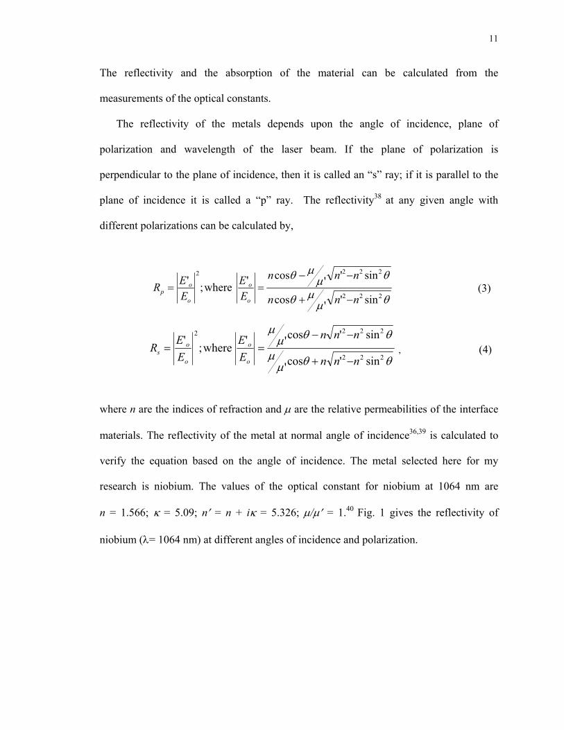
The reflectivity of the metals depends upon the angle of incidence, plane of
polarization and wavelength of the laser beam. If the plane of polarization is
perpendicular to the plane of incidence, then it is called an “s” ray; if it is parallel to the
plane of incidence it is called a “p” ray. The reflectivity38 at any given angle with
different polarizations can be calculated by,
θμ
μθ
θμμθ
222
2222
sin''cos
sin''cos' where;'
nnn
nnn
EE
EER
o
o
o
op
−+
−−== (3)
θθμ
μ
θθμμ
222
2222
sin'cos'
sin'cos'' where;
'
nnn
nnn
EE
EE
Ro
o
o
os
−+
−−== , (4)
where n are the indices of refraction and μ are the relative permeabilities of the interface
materials. The reflectivity of the metal at normal angle of incidence36,39 is calculated to
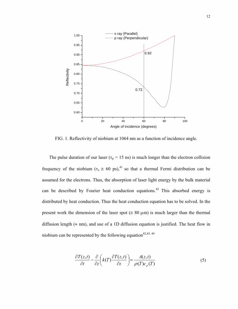
verify the equation based on the angle of incidence. The metal selected here for my
research is niobium. The values of the optical constant for niobium at 1064 nm are
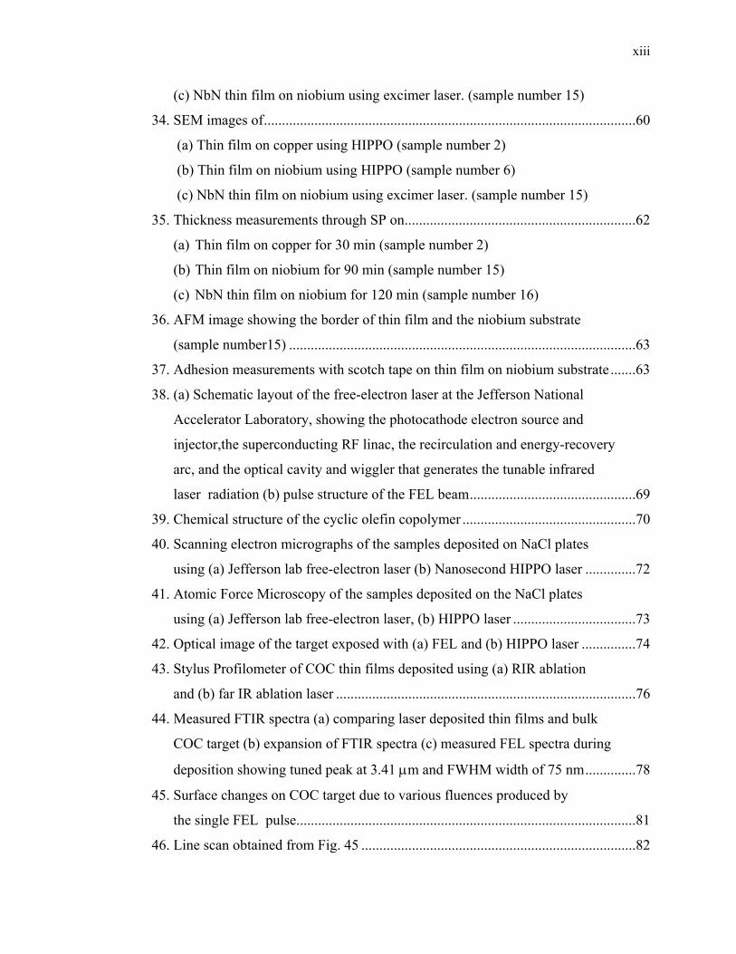
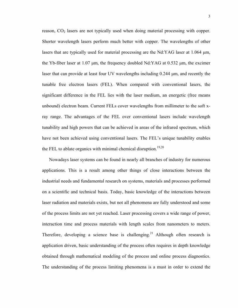
n = 1.566; κ = 5.09; n′ = n + iκ = 5.326; μ/μ′ = 1.40 Fig. 1 gives the reflectivity of
niobium (λ= 1064 nm) at different angles of incidence and polarization.
12
0 20 40 60 80 100
0.60
0.65
0.70
0.75
0.80
0.85
0.90
0.95
1.00
Ref
lect
ivity
Angle of incidence (degrees)
s ray (Parallel) p ray (Perpendicular)
0.72
0.92
FIG. 1. Reflectivity of niobium at 1064 nm as a function of incidence angle.
The pulse duration of our laser (τp = 15 ns) is much longer than the electron collision
frequency of the niobium (τe ≅ 60 ps),41 so that a thermal Fermi distribution can be
assumed for the electrons. Thus, the absorption of laser light energy by the bulk material
can be described by Fourier heat conduction equations.42 This absorbed energy is
distributed by heat conduction. Thus the heat conduction equation has to be solved. In the
present work the dimension of the laser spot (≅ 80 μm) is much larger than the thermal
diffusion length (≈ nm), and use of a 1D diffusion equation is justified. The heat flow in
niobium can be represented by the following equation42,43, 44
)()(
),(),()(),(TcT
tzAz
tzTTkzt
tzT
pρ=⎟
⎠⎞
⎜⎝⎛
∂∂
∂∂
−∂
∂ (5)
13
where T(z,t) is the temperature at depth z at time t, ρ is the mass density, is the
thermal diffusivity, and A(z,t) is the heat generation (source or which is the combination
of absorbed laser energy and internal heat sink) which can be written as
, 1 ∆ , , (6)
where ΔU(z,t) is the internal heat sink (phase transformation) and ,
which describes the Gaussian temporal laser pulse profile. The parameters used for our
experiment are σ = 6.37 ns (for 15 ns FWHM), πσ 2
HIo = and H is the fluence
(J/cm2). The reflectivity for niobium for the wavelength 1064 nm at an angle of 600 is
0.21 for parallel polarization and 0.68 for perpendicular polarization.
2
2
2)(
exp)( σott
oItI−−
=
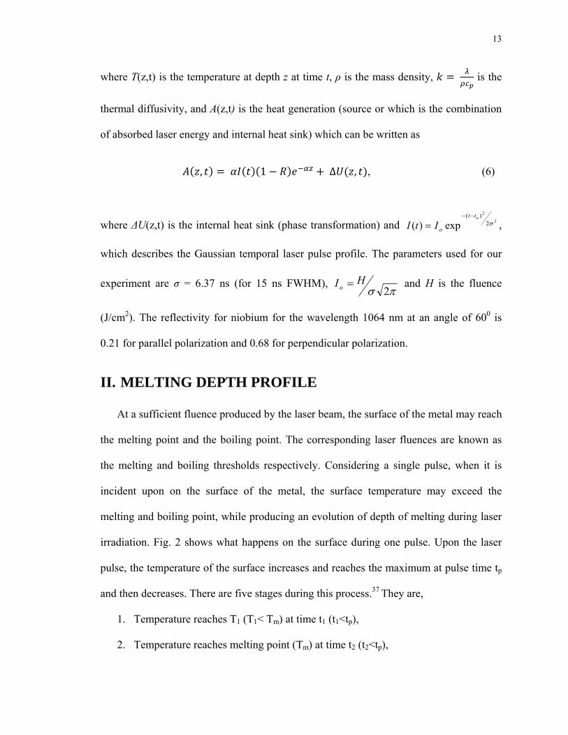
II. MELTING DEPTH PROFILE
At a sufficient fluence produced by the laser beam, the surface of the metal may reach
the melting point and the boiling point. The corresponding laser fluences are known as
the melting and boiling thresholds respectively. Considering a single pulse, when it is
incident upon on the surface of the metal, the surface temperature may exceed the
melting and boiling point, while producing an evolution of depth of melting during laser
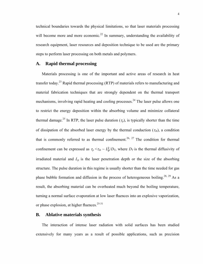
irradiation. Fig. 2 shows what happens on the surface during one pulse. Upon the laser
pulse, the temperature of the surface increases and reaches the maximum at pulse time tp
and then decreases. There are five stages during this process.37 They are,
1. Temperature reaches T1 (T1< Tm) at time t1 (t1<tp),
2. Temperature reaches melting point (Tm) at time t2 (t2<tp),
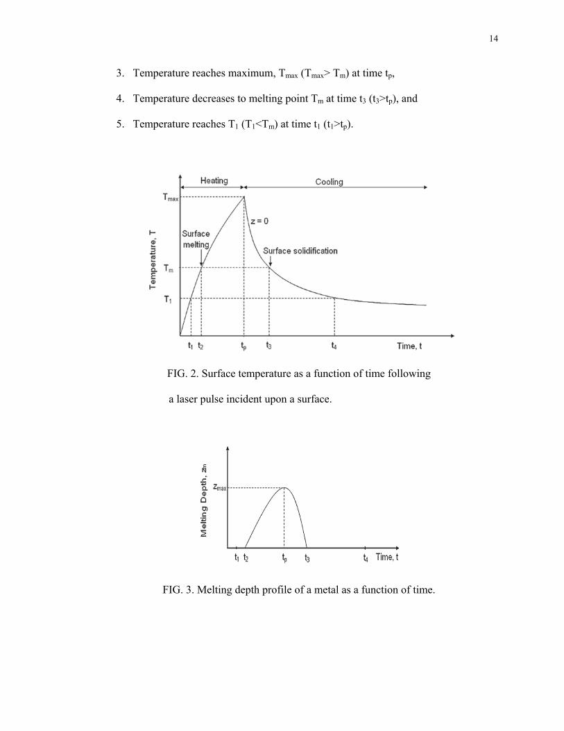
14
3. Temperature reaches maximum, Tmax (Tmax> Tm) at time tp,
4. Temperature decreases to melting point Tm at time t3 (t3>tp), and
5. Temperature reaches T1 (T1<Tm) at time t1 (t1>tp).
FIG. 2. Surface temperature as a function of time following
a laser pulse incident upon a surface.
FIG. 3. Melting depth profile of a metal as a function of time.
15
Fig. 3 shows the melting depth of a metal as a function of time. During irradiation,
the melting starts at time t2 only. Before that time, the material is just heated without any
changes. After t2, the depth of the melting increases, until it reaches the maximum solid-
liquid interface depth (zmax), which starts to decrease after the surface heating phase, after
the time tp. After time tp, the surface temperature starts to decrease rapidly, and the
solidification process starts. After the surface solidification time t3, the metal cools down
further.
III. SIMULATION FOR SURFACE TEMPERATURE
As there is no analytical solution to Eq. (5), we use the finite differences method
(forward difference approximation) to solve the equation. Time (t) and space (z) are
divided equally as, ti = iΔt and zn = nΔz (where n = 0…..N and z is the direction normal
pointing into the surface). Defining the function T whose value Ti is known at the discrete
points, the approximation of first and second order partial differential operators at point i
can be written as,
∆, and
2
2 1 2 1∆ 2 , (7)
where is the temperature at the time ti = iΔt in the layer zn = nΔz. The calculation
starts at i = 0 with 300 for all n. Evaluation of the first order derivative with
respect to time and the second order with respect to direction (here z direction),
substituting Eq. (7) into Eq. (5), we can write,
inT
∆ .∆
. 2,
, (8)
16
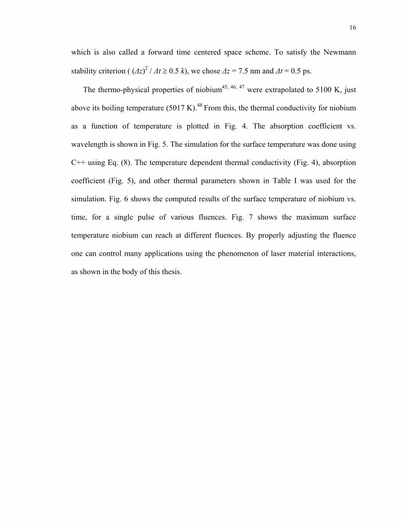
which is also called a forward time centered space scheme. To satisfy the Newmann
stability criterion ( (Δz)2 / Δt ≥ 0.5 k), we chose Δz = 7.5 nm and Δt = 0.5 ps.
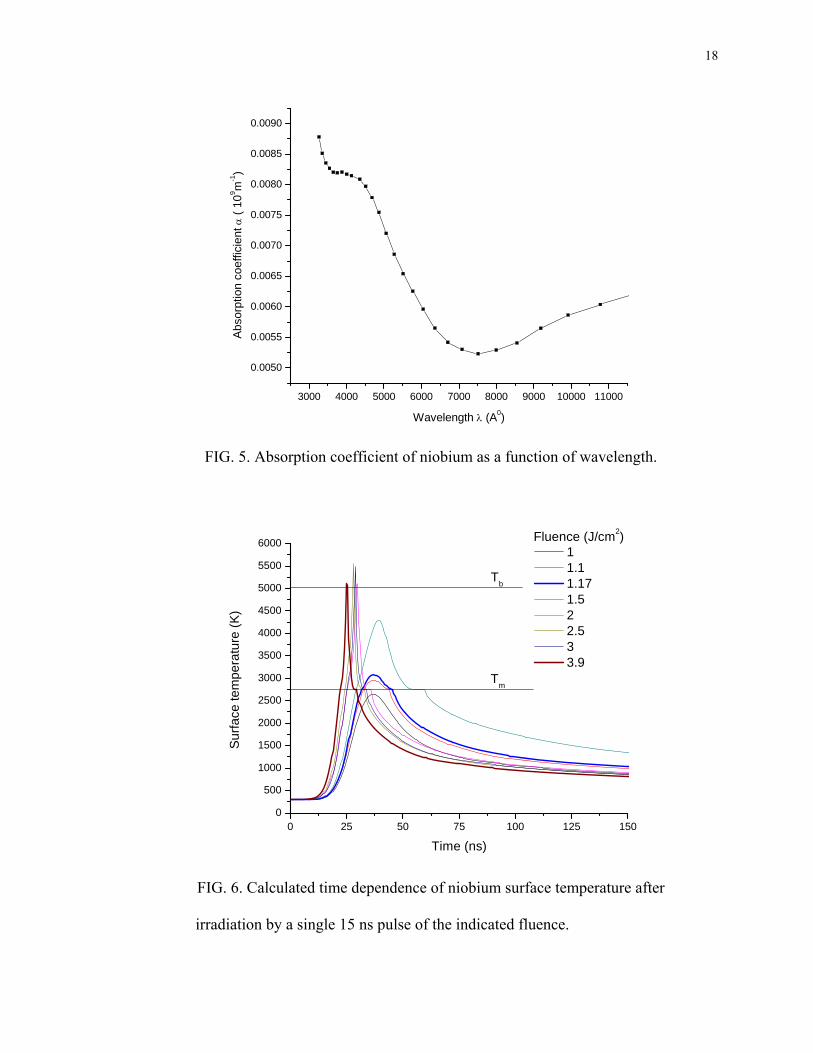
The thermo-physical properties of niobium45, 46, 47 were extrapolated to 5100 K, just
above its boiling temperature (5017 K).48 From this, the thermal conductivity for niobium
as a function of temperature is plotted in Fig. 4. The absorption coefficient vs.
wavelength is shown in Fig. 5. The simulation for the surface temperature was done using
C++ using Eq. (8). The temperature dependent thermal conductivity (Fig. 4), absorption
coefficient (Fig. 5), and other thermal parameters shown in Table I was used for the
simulation. Fig. 6 shows the computed results of the surface temperature of niobium vs.
time, for a single pulse of various fluences. Fig. 7 shows the maximum surface
temperature niobium can reach at different fluences. By properly adjusting the fluence
one can control many applications using the phenomenon of laser material interactions,
as shown in the body of this thesis.
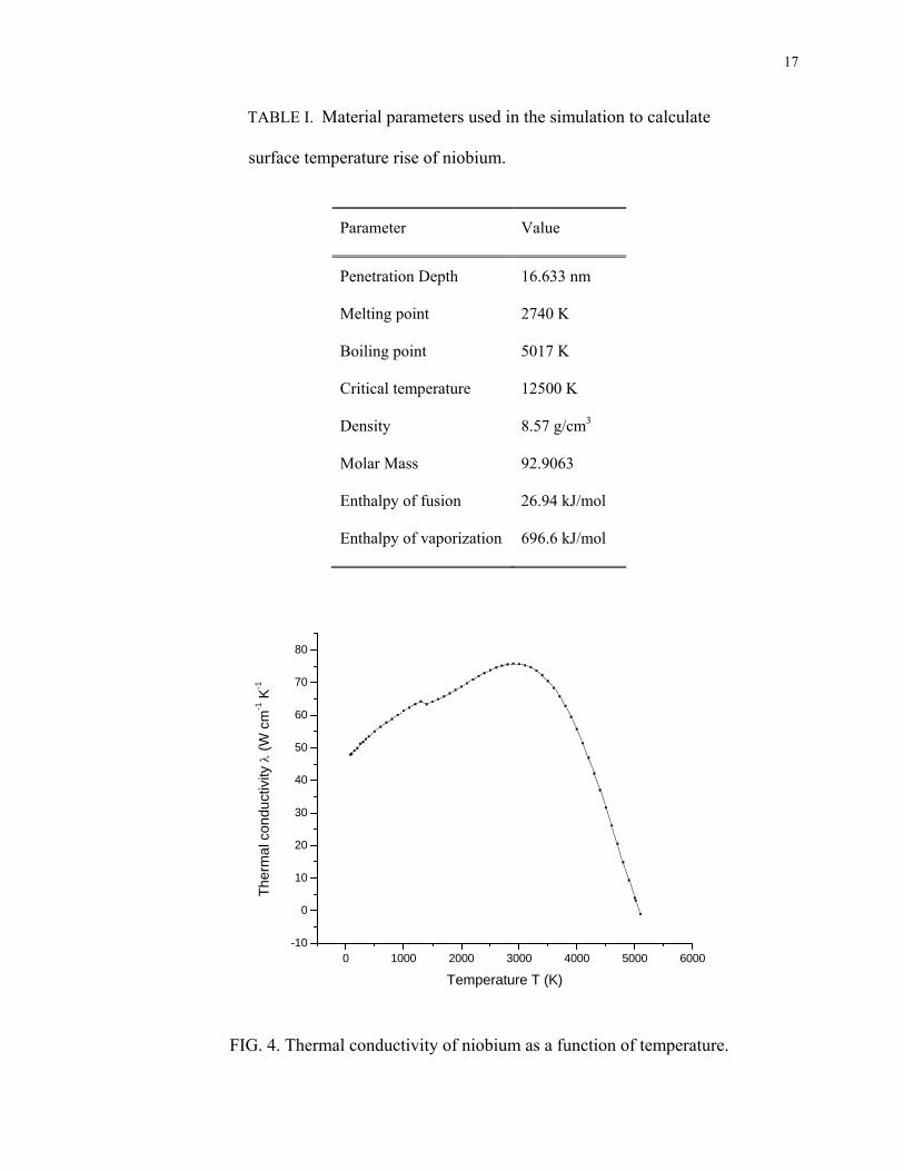
17
TABLE I. Material parameters used in the simulation to calculate
surface temperature rise of niobium.
Parameter Value
Penetration Depth 16.633 nm
Melting point 2740 K
Boiling point 5017 K
Critical temperature 12500 K
Density 8.57 g/cm3
Molar Mass 92.9063
Enthalpy of fusion 26.94 kJ/mol
Enthalpy of vaporization 696.6 kJ/mol
0 1000 2000 3000 4000 5000 6000-10
0
10
20
30
40
50
60
70
80
Ther
mal
con
duct
ivity
λ (W
cm
-1 K
-1
Temperature T (K)
FIG. 4. Thermal conductivity of niobium as a function of temperature.
18
3000 4000 5000 6000 7000 8000 9000 10000 11000
0.0050
0.0055
0.0060
0.0065
0.0070
0.0075
0.0080
0.0085
0.0090
Abso
rptio
n co
effic
ient
α (
109 m
-1)
Wavelength λ (A0)
FIG. 5. Absorption coefficient of niobium as a function of wavelength.
0 25 50 75 100 125 1500
500
1000
1500
2000
2500
3000
3500
4000
4500
5000
5500
6000
Tm
Surfa
ce te
mpe
ratu
re (K
)
Time (ns)
1 1.1 1.17 1.5 2 2.5 3 3.9
Fluence (J/cm2)
Tb
FIG. 6. Calculated time dependence of niobium surface temperature after
irradiation by a single 15 ns pulse of the indicated fluence.

19
0 1 2 3 4 5 6 7 8 9500
1000
1500
2000
2500
3000
3500
4000
4500
5000
5500
6000
6500
7000
Max
imum
sur
face
tem
pera
ture
T(K
)
Laser Fluence H ( J/cm2)
Tb
Tm
FIG. 7. Maximum surface temperature irradiated
by a single 15 ns pulse of various fluences.
IV. LASER POLISHING OF NIOBIUM FOR SRF
ACCELERATOR CAVITIES
Accelerators based on superconducting niobium RF cavities will play a growing role
in the future. Their science and technology has been recently reviewed.49 A key feature is
that, in the superconducting state, the RF field penetration is limited to the surface-
adjacent 40 nm, lending great importance to the composition and topography of the
cavity interior surface. Accordingly, the final steps of present day cavity fabrication
methods seek to remove damaged or contaminated material by etching off approximately
100 μm. A disadvantage of this etching process is that it uses aggressive acids
(hydrofluoric, nitric, sulfuric) creating cost, safety, and environmental impact issues.
20
The use of lasers to smooth metal surfaces began to be reported in the 1970’s and
several processing strategies have evolved since. A recent review presents the history, the
fundamentals, and the process applications.33 The broad theme in laser polishing is that
the laser energy melts some of or the entire surface and leveling proceeds by melt flow
under the influence of surface tension until solidification intervenes. The events may be
viewed in terms of lower and higher energy density regimes, shallow surface melting
(SSM) and surface over-melting (SOM), respectively.50 In SSM, melting occurs at
prominences and capillary forces cause the melt to diffuse into depressions. In SSM, a
liquid layer covers the surface. While surface tension driven leveling proceeds, other
mechanisms can give rise to oscillations manifest as regular ridge structures.
Laser surface melting (LSM) is also used to process surfaces to achieve superior
bonding of deposited layers, reduced distortion, and improved physical properties, e.g.,
increased hardness, wear resistance, and corrosion resistance.51 For example, laser
polishing of micro-milled nickel and titanium alloy parts reduced roughness more than
85%.52 Others53-55 used pulsed laser micro-polishing (PLμP) to reduce the surface
roughness of micro-fabricated and micro-milled parts. A significant range of pulse
durations and spot sizes has been effective.56,57 Pulse durations in the nanosecond range
were found most effective for SMM.58 The most recent reports include laser induced
surface finishing of titanium for bio-implants59,60 and micro-roughness reduction of
tungsten films in the IC industry.61 At the opposite end of the size scale, mobile laser
polishing is being investigated for application to railroad rail.62
Characterizing the resulting surface topography is a challenging task, as it is unknown
at what scale roughness is important to SRF performance; a recent review is available.63

21
The traditional parameter characterizing surface topography is the RMS roughness (Rq),
the root mean square height of a surface around its mean value. However, this statistical
description, though simple and reliable, makes no distinction between peaks and valleys
and does not account for the lateral distribution of surface features. A more complete
description is provided by the PSD (power spectral density), which performs a
decomposition of the surface profile into its spatial wavelengths and allows comparison
of roughness measurements over different spatial distance ranges.
The present work gives results obtained by laser melting to smooth the surface of
niobium. The resulting topography was examined by scanning electron microscopy
(SEM) and atomic force microscopy (AFM). PSD’s were computed from AFM data.
V. EXPERIMENTAL DETAILS
A. Fluence range to be explored
Laser polishing requires that each pulse heats the surface to a temperature between
melting and boiling for the longest possible time, so that surface tension can act. We
employed computational modeling to predict the time course of the surface temperature
as a function of the laser irradiation parameters. The goal is to identify the most
promising range of experimental parameters. So the laser fluences between 0.6 to
2.3 J/cm2, based on Figs. 6 and 7, were explored. To additionally gain insight into the
effect of work piece preheat; calculations were carried out assuming the initial surface
temperature to be 300K, 473 K, or 673 K.
Fig. 8 shows the calculated surface temperature of niobium vs. fluence, for a single
pulse at the three initial surface temperatures. This predicts that for a single pulse, surface
melting starts at about 1.1 J/cm2 when the initial surface temperature is at 300 K. When

22
the initial surface temperature is 473 K or 673 K, the surface reaches the melting
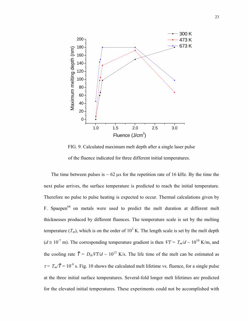
temperature at 1 J/cm2. Overall, Fig. 8 indicates that the fluence range from 1 J/cm2 to
2 J/cm2 should be explored. Fig. 9 shows the simulated maximum melting depth vs.
fluence for a single pulse at the three initial surface temperatures. It indicates that at the
low end of the fluence range of interest, the calculated melt depth may not exceed the RF
penetration depth.
1.0 1.5 2.0 2.5 3.0
2500
3000
3500
4000
4500
5000
5500
Tm
Tb
Max
imum
sur
face
tem
pera
ture
(K)
Fluence (J/cm2)
300 K 473 K 673 K
FIG. 8. Calculated peak surface temperature after a single laser pulse of
the fluence indicated for three initial temperatures.
23
1.0 1.5 2.0 2.5 3.0
0
20
40
60
80
100
120
140
160
180
200
Max
imum
mel
ting
dept
h (n
m)
Fluence (J/cm2)
300 K 473 K 673 K
FIG. 9. Calculated maximum melt depth after a single laser pulse
of the fluence indicated for three different initial temperatures.
The time between pulses is ~ 62 μs for the repetition rate of 16 kHz. By the time the
next pulse arrives, the surface temperature is predicted to reach the initial temperature.
Therefore no pulse to pulse heating is expected to occur. Thermal calculations given by
F. Spaepen64 on metals were used to predict the melt duration at different melt
thicknesses produced by different fluences. The temperature scale is set by the melting
temperature (Tm), which is on the order of 103 K. The length scale is set by the melt depth
(d ≅ 10-7 m). The corresponding temperature gradient is then ∇T = Tm/d ~ 1010 K/m, and
the cooling rate Ť = Dth∇T/d ~ 1012 K/s. The life time of the melt can be estimated as
τ = Tm/Ť = 10-9 s. Fig. 10 shows the calculated melt lifetime vs. fluence, for a single pulse
at the three initial surface temperatures. Several-fold longer melt lifetimes are predicted
for the elevated initial temperatures. These experiments could not be accomplished with

24
our current experimental setup, but will be undertaken in the future. The present
experiments aim at shallow penetration and short melt lifetime, seeking to maximize the
SMM contribution.
1.0 1.5 2.0 2.5 3.0
0.0
2.0x10⁻¹⁰
4.0x10⁻¹⁰
6.0x10⁻¹⁰
8.0x10⁻¹⁰
1.0x10⁻⁹
1.2x10⁻⁹
1.4x10⁻⁹
1.6x10⁻⁹
Mel
t life
tim
e (s
)
Fluence (J/cm2)
300K 473K 673K
FIG. 10. Calculated melt life time for a single laser pulse of
the fluence indicated for three different initial temperatures.
B. Experimental setup & procedure
A PVD Products Inc. PLD 5000 system was used for the experiments. Processing was
carried out in a vacuum chamber evacuated to 10-7 Torr by a rotary backed turbo pump. A
reflecting mirror placed in the optical train was used to raster the laser beam over a radial
range on the target up to ~1.8 inch. The target pedestals can hold targets of 50 mm in
diameter and can rotate individually with a maximum speed of 12 rpm. In each run, three
bare niobium discs were mounted and the rotation speed was varied according to the
25
experiment to obtain the intended pulse accumulation. The laser fluence and pulse
accumulation are the experimental parameters explored in this study. The laser beam was
incident at an angle of 60o from normal on the rotating niobium target. The laser used
was a Spectra Physics “High Intensity Peak Power Oscillator” (HIPPO) Nd:YAG
(λ = 1064 nm, Emax= 0.430 mJ, τp = 15 ns, beam spot ≅ 80 μm). The 1/e2 beam intensity
width (w = 2σ) was determined with a SPIRICON laser beam profiler fitting to a
Gaussian transverse intensity distribution . The measured energy per
pulse (u) at the target and measured D4σ width (2w) are combined to give the measured
fluence (H) in J/cm2 using Eq. (9),
cos 60 (9)
where 600 is the angle the incident laser beam makes with the surface normal. This
angular correction factor gives the energy flux in the normal direction suitable for
comparison to the 1-D calculations. Laser fluences of 0.6 to 2.3 J/cm2 were focused on
the niobium target, intending to traverse the temperature from below melting to above
boiling, seeking to probe both the SMM and SOM regimes. See Appendix A for more
details about the PLD 5000 system and the HIPPO.
Niobium discs, 50 mm in diameter and 2-3 mm thick were cut from polycrystalline
sheet stock used for SRF cavities. The samples were degreased in a detergent with
ultrasonic agitation, buffered chemically polished in a 1:1:2 solutions of hydrofluoric acid
(49%), nitric acid (69.5%), and phosphoric acid (85%), and subsequently rinsed with
26
ultrapure water followed by a high pressure rinsing for 1 hour. The etching was done for
about 2 minutes, removing approximately 10 µm from the surface of each disc.
To make melting evident, the disc surfaces were roughened using 600 grit sandpaper
(approximate particle size: 15 μm). The discs were placed in the target holder and the
chamber was pumped down to 10-7 Torr. The laser fluence was varied from 0.6 to 2.3
J/cm2, with the number of pulses per unit area constant for the first set of experiments.
The target rotation and the repetition rates were adjusted to make sure the number of
pulses (same energy per pulse) that overlap on an area remains constant at 75 for this set
of tests. To understand the effect of pulse accumulation per area, a second set of
experiments were performed by keeping the laser fluence constant at 1.1 J/cm2 and
varying the number of pulses accumulated.
C. Surface Roughness Measurement
The present work gives results obtained by laser melting to smooth the surface of
niobium. The surface topography was investigated with a FE-SEM (Hitachi 4700
SEM/EDX) and with an atomic force microscope (Digital Instruments Nanoscope IV) in
tapping mode using silicon tips with 10 nm diameter. A series of 50 μm × 50 μm areas
were scanned on each sample.
PSD analysis of AFM data offers a more complete description than the RMS
roughness and provides useful quantitative information about the surface topography.
Appropriate analytical models aid interpretation and understanding of such morphologies
more quantitatively.65 Here we have adopted the definition used previously for the 2-D
PSD of a surface described by its topography z (x; y).65, 66
27
As before,63 the AFM scan data were detrended by removing a least squares two
dimensional first order polynomial from each record before further analysis. In this study,
the PSD profiles that were measured at different locations under the same scan condition
were averaged separately. A Tukey window transform was applied in order to eliminate
spurious high-frequency noise. PSD’s were calculated and averaged from at least three
scans from different areas. Since the surface after polishing will reveal some level of non
uniformity, averaging can effectively and accurately smooth out noise and give more
statistically representative PSD.
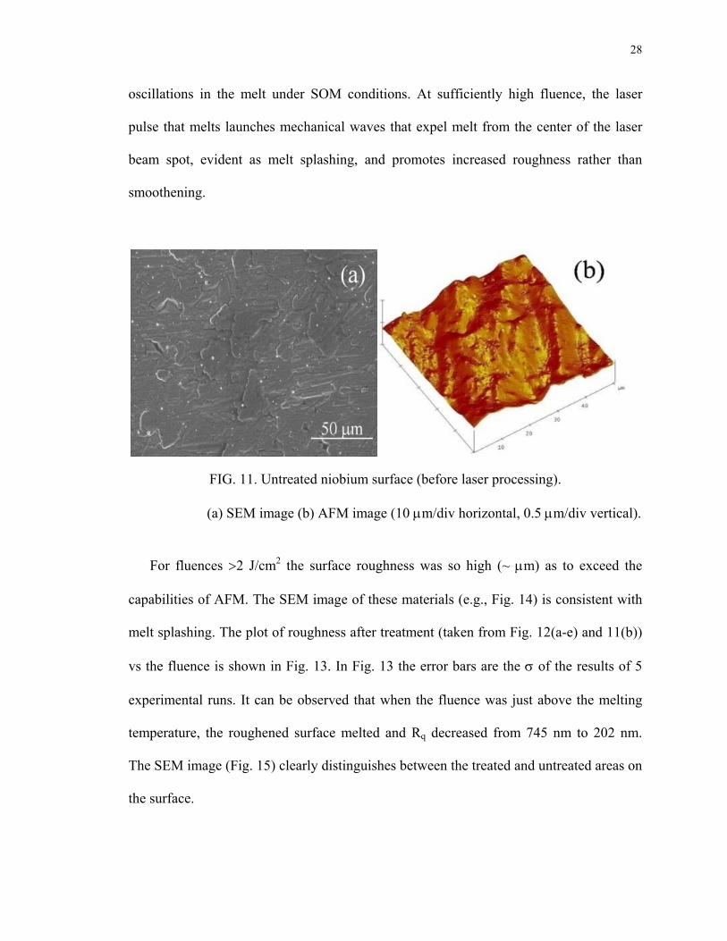
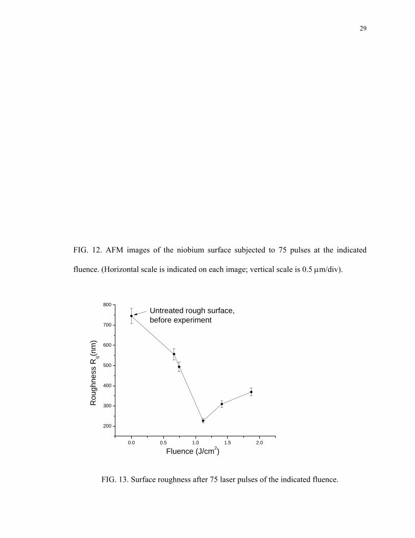
VI. RESULTS AND DISCUSSION
Figures 11(a) and 11(b) show SEM and AFM images of the untreated niobium
surface. The AFM data indicated a roughness (Rq) of 745 nm. Fig. 12 shows the series of
images from the first set of experiments, in which pulse energy was varied for a constant
number of pulses. In agreement with the calculations (Fig. 8), fluence less than 1 J/cm2
produced no visually obvious evidence of surface melting. Still, the roughness was
reduced from 745 nm (Fig. 11(b)) to 556 nm (Fig. 12(a)) or 493 nm (Fig. 12(b)). The
laser used in these experiments produces a Gaussian beam so that the fluence at the
center exceeds the average, perhaps causing a small amount of local melting for fluences
less than the value calculated to cause melting by a uniform beam. The fluence per pulse
predicted to reach just above the melting point of niobium (Fig. 12(c)) resulted in
rounding of sharp edges and smoothening of the surface to a roughness of 202 nm. We
interpret these findings as an increasing degree of SSM, with SOM beginning to be
evident. Once the fluence per pulse was increased further above the melting point, the
surface roughness increased (Fig. 12(d) and 12(e)), as would be expected from
28
oscillations in the melt under SOM conditions. At sufficiently high fluence, the laser
pulse that melts launches mechanical waves that expel melt from the center of the laser
beam spot, evident as melt splashing, and promotes increased roughness rather than
smoothening.
FIG. 11. Untreated niobium surface (before laser processing).
(a) SEM image (b) AFM image (10 μm/div horizontal, 0.5 μm/div vertical).
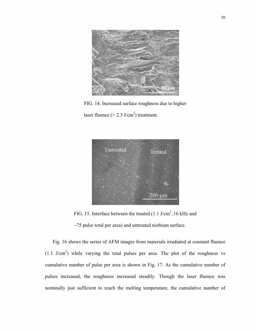
For fluences >2 J/cm2 the surface roughness was so high (~ μm) as to exceed the
capabilities of AFM. The SEM image of these materials (e.g., Fig. 14) is consistent with
melt splashing. The plot of roughness after treatment (taken from Fig. 12(a-e) and 11(b))
vs the fluence is shown in Fig. 13. In Fig. 13 the error bars are the σ of the results of 5
experimental runs. It can be observed that when the fluence was just above the melting
temperature, the roughened surface melted and Rq decreased from 745 nm to 202 nm.
The SEM image (Fig. 15) clearly distinguishes between the treated and untreated areas on
the surface.
29
FIG. 12. AFM images of the niobium surface subjected to 75 pulses at the indicated
fluence. (Horizontal scale is indicated on each image; vertical scale is 0.5 μm/div).
0.0 0.5 1.0 1.5 2.0
200
300
400
500
600
700
800
Rou
ghne
ss R
q(nm
)
Fluence (J/cm2)
Untreated rough surface,before experiment
FIG. 13. Surface roughness after 75 laser pulses of the indicated fluence.
30
FIG. 14. Increased surface roughness due to higher
laser fluence (> 2.3 J/cm2) treatment.
FIG. 15. Interface between the treated (1.1 J/cm2, 16 kHz and
~75 pulse total per area) and untreated niobium surface.
Fig. 16 shows the series of AFM images from materials irradiated at constant fluence
(1.1 J/cm2) while varying the total pulses per area. The plot of the roughness vs
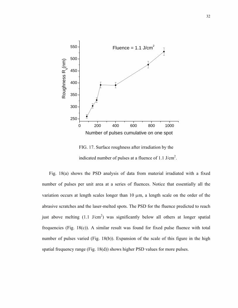
cumulative number of pulse per area is shown in Fig. 17. As the cumulative number of
pulses increased, the roughness increased steadily. Though the laser fluence was
nominally just sufficient to reach the melting temperature, the cumulative number of
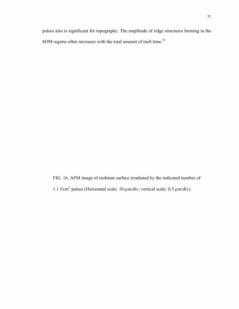
31
pulses also is significant for topography. The amplitude of ridge structures forming in the
SOM regime often increases with the total amount of melt time.33
FIG. 16. AFM image of niobium surface irradiated by the indicated number of
1.1 J/cm2 pulses (Horizontal scale: 10 μm/div; vertical scale: 0.5 μm/div).
32
0 200 400 600 800 1000
250
300
350
400
450
500
550
Rou
ghne
ss R
q(nm
)
Number of pulses cumulative on one spot
Fluence = 1.1 J/cm2
FIG. 17. Surface roughness after irradiation by the
indicated number of pulses at a fluence of 1.1 J/cm2.
Fig. 18(a) shows the PSD analysis of data from material irradiated with a fixed
number of pulses per unit area at a series of fluences. Notice that essentially all the
variation occurs at length scales longer than 10 μm, a length scale on the order of the
abrasive scratches and the laser-melted spots. The PSD for the fluence predicted to reach
just above melting (1.1 J/cm2) was significantly below all others at longer spatial
frequencies (Fig. 18(c)). A similar result was found for fixed pulse fluence with total
number of pulses varied (Fig. 18(b)). Expansion of the scale of this figure in the high
spatial frequency range (Fig. 18(d)) shows higher PSD values for more pulses.
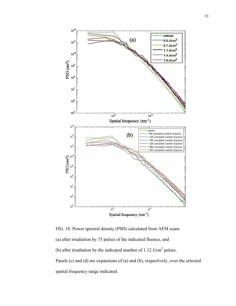
33
FIG. 18. Power spectral density (PSD) calculated from AFM scans
(a) after irradiation by 75 pulses of the indicated fluence, and
(b) after irradiation by the indicated number of 1.12 J/cm2 pulses.
Panels (c) and (d) are expansions of (a) and (b), respectively, over the selected
spatial frequency range indicated.

34
FIG. 18. Continued
VII. CONCLUSION
Parameters were found for irradiating niobium with a nanosecond laser that produced
a significant reduction of surface roughness. PSD analysis of the AFM topography data
revealed that a major effect was in the spatial frequency range longer than 10 μm,
consistent with the notion of melt oscillations and splashing at high fluence. We conclude

35
that both SMM and SOM were contributing under the conditions leading to the greatest
roughness reduction. A computational model based on the effect of single, spatially-
uniform pulses provided useful predictions even though the present experiments used
multiple pulses of a Gaussian beam.
36
CHAPTER 3
LASER NITRIDING OF NIOBIUM FOR
APPLICATION TO
SRF ACCELERATOR CAVITIES
I. INTRODUCTION
The BCS surface resistance of niobium at 1.3 GHz decreases from about 800 nΩ at
4.2 K to 15 nΩ at 2 K.49 The quality factor Q0 (2π times the ratio of stored energy to
energy loss per cycle) is inversely proportional to the surface resistance and may exceed
1010. The strong temperature dependence of the resistance is the reason why operation at
1.8 – 2 K is essential for achieving high accelerating gradients in combination with very
high quality factors (and thus energy efficiency). Moreover, superfluid helium is an
excellent coolant owing to its high heat conductivity. The thermal conductivity of
niobium at cryogenic temperatures is strongly temperature dependent and drops by about
an order of magnitude when lowering the temperature from 4.2 K to ~2 K.67 In principle,
forming the active interior surface from superconducting niobium nitride (Tc ≈ 17 K) vs.
the present niobium (Tc ≈ 9.2 K) would reduce cryogenic costs and simplify cavity
engineering. The required thickness of the NbN layer needs to take account of the
London penetration depth, reported variously as 85 nm,68 176 nm,69 270 nm70 and 375
nm71 for different NbN preparation schemes.
37
The Nb-N phase diagram was reported.72 The desired δNbN extends from ~42 to
50 atomic percent nitrogen. The fcc δ phase converts to the hcp ε phase upon cooling
below 1300 oC; ε is not superconducting. Furnace nitriding studies have not been able to
obtain δNbN.73 Quenching from above 1300 oC has yielded some of the desired phase.74
Rapid thermal processing with a pulsed heat lamp of Nb films on Si in nitrogen yielded
some δNbN.75 Accordingly, we investigated the very rapid cooling attainable by self-
quenching in gas/laser nitriding.
P. Schaaf reported laser gas nitriding of iron,43 aluminum, and titanium,76 but there
appears to have been no work on solid niobium. Compared to furnace nitriding, laser
nitriding offers the advantages of a rapid quench, a high nitrogen concentration, fast
treatment, and precise position control. Furthermore, materials sensitive to heat and of
complex shape can be successfully laser treated. Such considerations motivate our
experiment to nitride niobium, obtaining δNbN by laser nitriding.
II. EXPERIMENTAL DETAILS
A. Fluence range to be explored
In the most desirable process, the niobium surface will be heated to just above the
boiling temperature and then cooled rapidly to avoid the δ→ε conversion. We employ
computational modeling to predict the time course of the surface temperature as a
function of the laser irradiation parameters. The goal is to identify the most promising
range of parameters to guide selection of experimental conditions.
Fig. 6, shows the surface temperature profile of niobium vs time, for a single 15 ns
pulse of various fluences. The surface temperature profile predicts that surface melting
38
starts at about 1.1 J/cm2, and the boiling temperature is reached at 2 J/cm2. To produce
the superconducting δNbN, it is desirable that the fluence brings the surface temperature
to just above the boiling point to facilitate reaction with the nitrogen atmosphere, but not
to ablate the material. The thickness of the nitride layer is expected to increase with dwell
time above melting,47 so fluences above 2 J/cm2 were explored.
The photon energy of the laser at the wavelength 1064 nm is only 1.1eV,77 which is
too low to interact directly with the nitrogen atmosphere inside the chamber, which has
an ionization energy of 15.6 eV and a dissociation energy of 9.8 eV.78 The laser intensity
is low enough that gas breakdown cannot occur, which needs a threshold intensity of
3x 10¹⁰ W/cm2.32, 79 The threshold can be reduced by two orders of magnitude when a
metal surface is place in the nitrogen atmosphere.80 So we conclude the laser will react
only on the niobium surface and not with the nitrogen present in the chamber.
B. Experimental setup & procedure
A PVD Products Inc. PLD 5000 system was used to carry out the experiments. The
niobium discs (2” in diameter, 2-3 mm thickness) were cut from sheet stock used for SRF
cavities. The chemical etching was carried out by buffered chemical polishing (BCP) to
clean the surface. About 10 microns was removed from the surface of each disc. Fig. 19
shows the picture of the niobium disc before treating with the laser.
Laser processing is carried out in a vacuum chamber evacuated by a rotary backed
turbo pump to 10-7 Torr. Following evacuation, the chamber can be backfilled with pure
nitrogen gas (99.999%) at a pressure ranging from 450 Torr to 620 Torr. The laser
irradiation was carried out in this atmosphere. To produce thermal energy for nitriding, a
Spectra Physics, “High Intensity Peak Power Oscillator” (HIPPO) nanosecond laser (λ =
39
1064 nm, Emax= 0.430 mJ, τp =15ns, beam spot ≅ 80 μm) was used. Laser fluences in the
range from 2.5 J/cm2 to 6 J/cm2per pulse were delivered (Fig. 20), intending that the
niobium surface reaches above its boiling temperature. In the nitrogen atmosphere, the
laser beam is incident at an angle of 60o from normal of the rotating niobium target. The
target rotation was kept constant at 9 rpm. The rastering mirror was programmed to scan
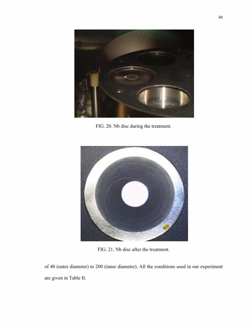
in such a way that the laser irradiated concentric circles on the niobium target, where
reaction with nitrogen gas was intended to form NbN. The combination of the
experimental parameters produces concentric circles (graded treatment) on the niobium
surface. Fig. 21 shows the laser irradiated niobium disc after the experiment. Thus the
number of pulses (same energy per pulse) overlapping is inversely proportional to the
radius of the rings, yielding a varying thickness of NbN layer across the nitrided area.
Each irradiated ring was subjected to a total laser pulse number per unit area in the range
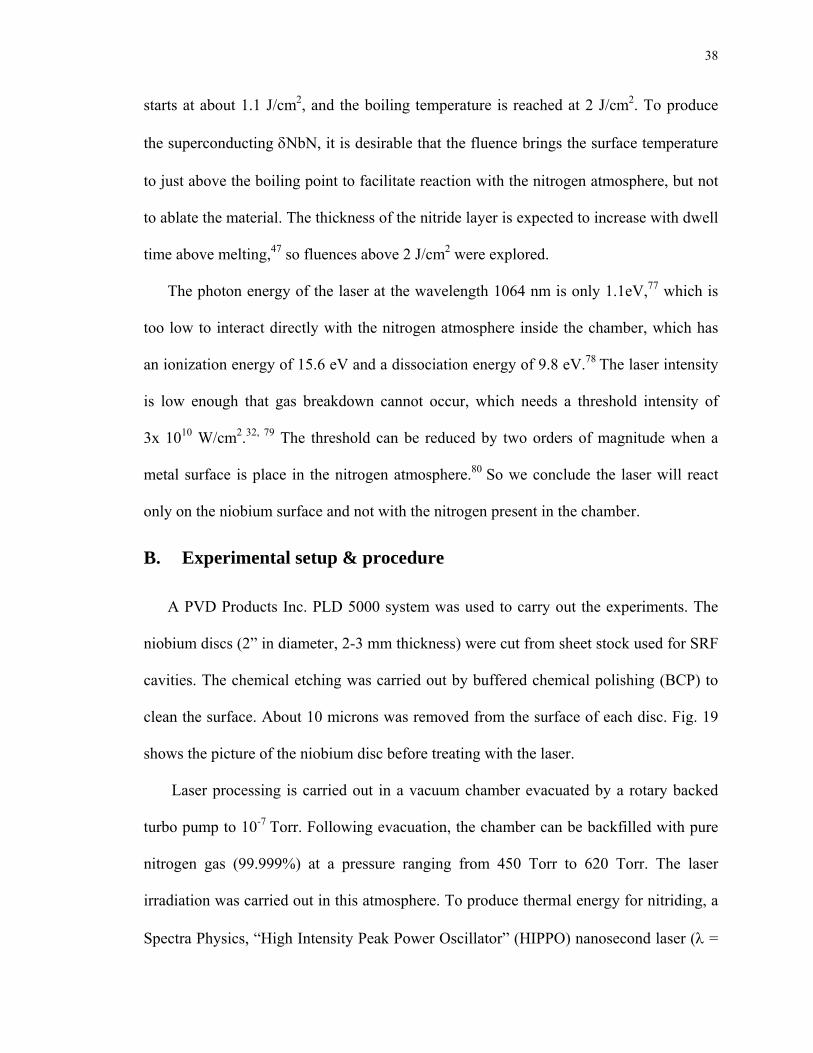
FIG. 19. Nb disc before treatment.
40
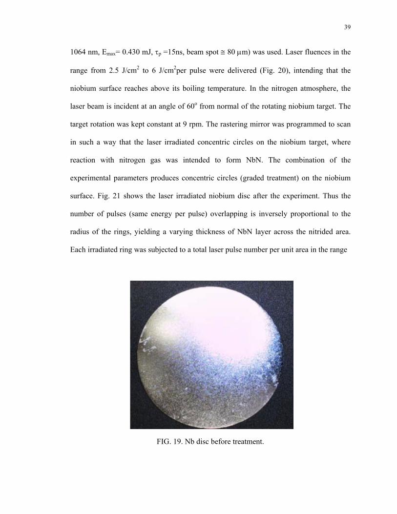
FIG. 20. Nb disc during the treatment.
FIG. 21. Nb disc after the treatment.
of 40 (outer diameter) to 200 (inner diameter). All the conditions used in our experiment
are given in Table II.
41
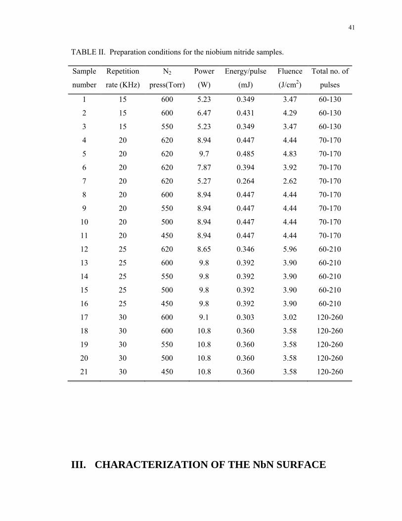
TABLE II. Preparation conditions for the niobium nitride samples.
Sample
number
Repetition
rate (KHz)
N2
press(Torr)
Power
(W)
Energy/pulse
(mJ)
Fluence
(J/cm2)
Total no. of
pulses
1 15 600 5.23 0.349 3.47 60-130
2 15 600 6.47 0.431 4.29 60-130
3 15 550 5.23 0.349 3.47 60-130
4 20 620 8.94 0.447 4.44 70-170
5 20 620 9.7 0.485 4.83 70-170
6 20 620 7.87 0.394 3.92 70-170
7 20 620 5.27 0.264 2.62 70-170
8 20 600 8.94 0.447 4.44 70-170
9 20 550 8.94 0.447 4.44 70-170
10 20 500 8.94 0.447 4.44 70-170
11 20 450 8.94 0.447 4.44 70-170
12 25 620 8.65 0.346 5.96 60-210
13 25 600 9.8 0.392 3.90 60-210
14 25 550 9.8 0.392 3.90 60-210
15 25 500 9.8 0.392 3.90 60-210
16 25 450 9.8 0.392 3.90 60-210
17 30 600 9.1 0.303 3.02 120-260
18 30 600 10.8 0.360 3.58 120-260
19 30 550 10.8 0.360 3.58 120-260
20 30 500 10.8 0.360 3.58 120-260
21 30 450 10.8 0.360 3.58 120-260
III. CHARACTERIZATION OF THE NbN SURFACE
42
The crystal structure of the surface was determined by x-ray diffraction (XRD) using
a Panalytical X’Pert instrument with Co Kα radiation. Phases on the surface were
identified by matching the diffraction peaks with the JCPDS (Joint Committee on Powder
Diffraction Standards) card. The surface topography was investigated by FE-SEM
(Hitachi 4700 SEM/EDX). This was also used to examine in cross-section the thickness
of the NbN layer on the Nb. The concentration of nitrogen in the niobium was
investigated by energy dispersive x-ray spectroscopy (EDS) on the SEM and wavelength
dispersive x-ray spectroscopy on the electron probe microanalysis (EPMA).
IV. RESULTS AND DISCUSSION
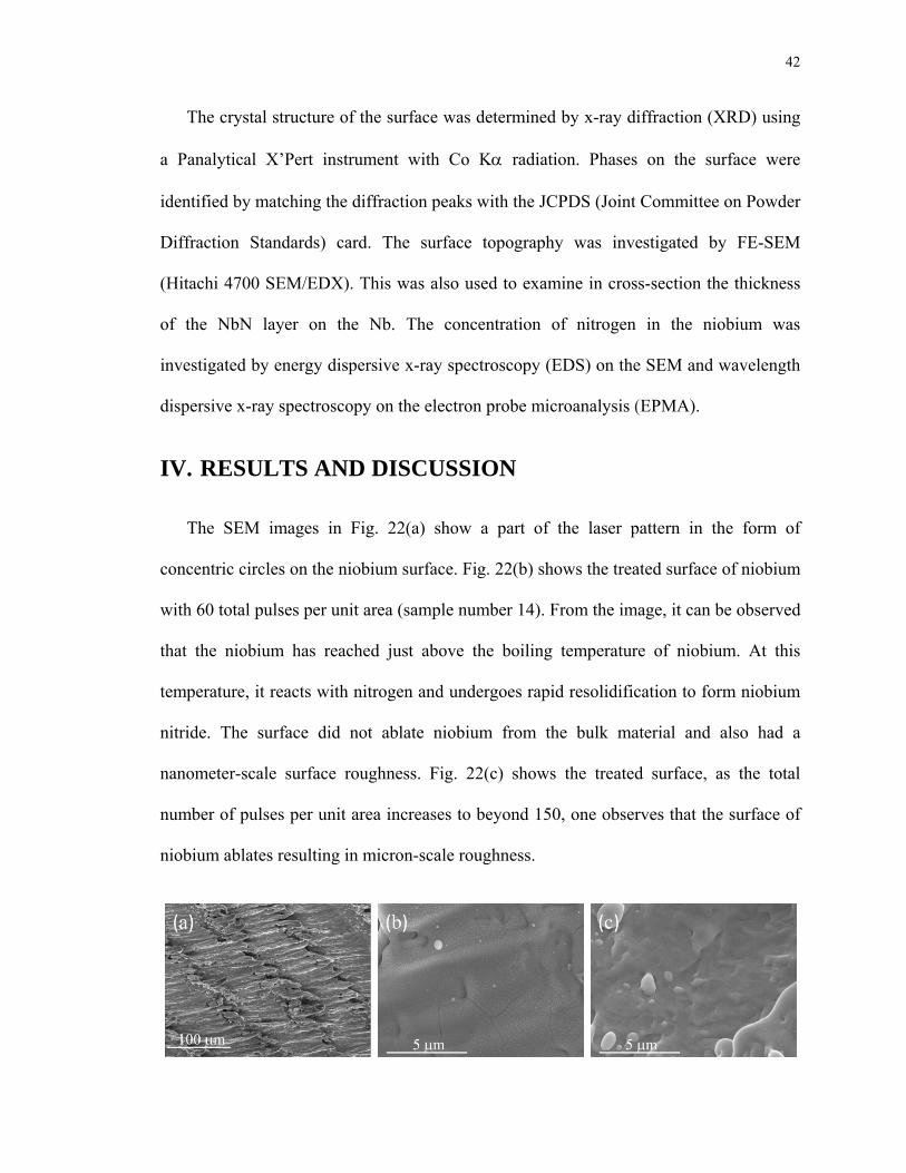
The SEM images in Fig. 22(a) show a part of the laser pattern in the form of
concentric circles on the niobium surface. Fig. 22(b) shows the treated surface of niobium
with 60 total pulses per unit area (sample number 14). From the image, it can be observed
that the niobium has reached just above the boiling temperature of niobium. At this
temperature, it reacts with nitrogen and undergoes rapid resolidification to form niobium
nitride. The surface did not ablate niobium from the bulk material and also had a
nanometer-scale surface roughness. Fig. 22(c) shows the treated surface, as the total
number of pulses per unit area increases to beyond 150, one observes that the surface of
niobium ablates resulting in micron-scale roughness.
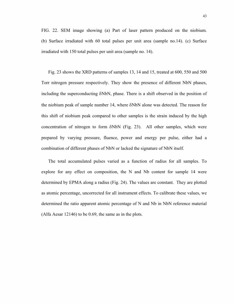
43
FIG. 22. SEM image showing (a) Part of laser pattern produced on the niobium.
(b) Surface irradiated with 60 total pulses per unit area (sample no.14). (c) Surface
irradiated with 150 total pulses per unit area (sample no. 14).
Fig. 23 shows the XRD patterns of samples 13, 14 and 15, treated at 600, 550 and 500
Torr nitrogen pressure respectively. They show the presence of different NbN phases,
including the superconducting δNbN, phase. There is a shift observed in the position of
the niobium peak of sample number 14, where δNbN alone was detected. The reason for
this shift of niobium peak compared to other samples is the strain induced by the high
concentration of nitrogen to form δNbN (Fig. 23). All other samples, which were
prepared by varying pressure, fluence, power and energy per pulse, either had a
combination of different phases of NbN or lacked the signature of NbN itself.
The total accumulated pulses varied as a function of radius for all samples. To
explore for any effect on composition, the N and Nb content for sample 14 were
determined by EPMA along a radius (Fig. 24). The values are constant. They are plotted
as atomic percentage, uncorrected for all instrument effects. To calibrate these values, we
determined the ratio apparent atomic percentage of N and Nb in NbN reference material
(Alfa Aesar 12146) to be 0.69, the same as in the plots.
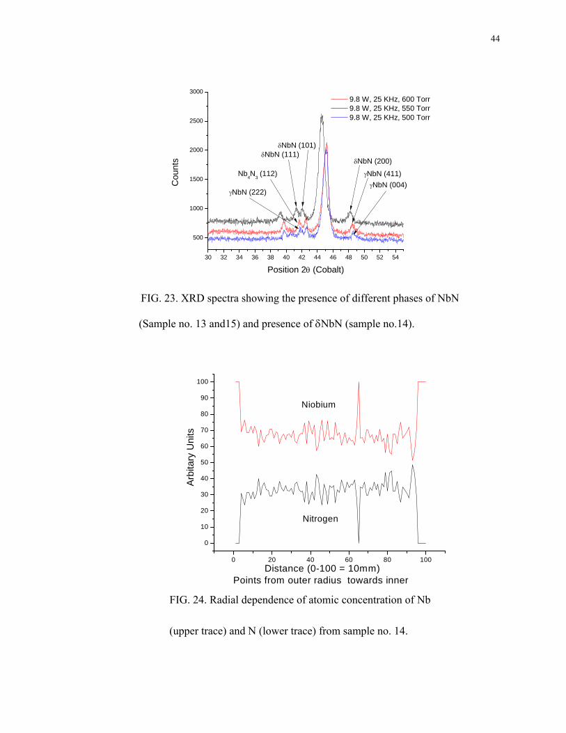
44
30 32 34 36 38 40 42 44 46 48 50 52 54
500
1000
1500
2000
2500
3000
γNbN (004)γNbN (222)
Nb4N3 (112) γNbN (411)
δNbN (200)δNbN (111)
δNbN (101)
Cou
nts
Position 2θ (Cobalt)
9.8 W, 25 KHz, 600 Torr 9.8 W, 25 KHz, 550 Torr 9.8 W, 25 KHz, 500 Torr
FIG. 23. XRD spectra showing the presence of different phases of NbN
(Sample no. 13 and15) and presence of δNbN (sample no.14).
0 20 40 60 80 100
0
10
20
30
40
50
60
70
80
90
100
Arb
itary
Uni
ts
Distance (0-100 = 10mm)Points from outer radius towards inner
Niobium
Nitrogen
FIG. 24. Radial dependence of atomic concentration of Nb
(upper trace) and N (lower trace) from sample no. 14.
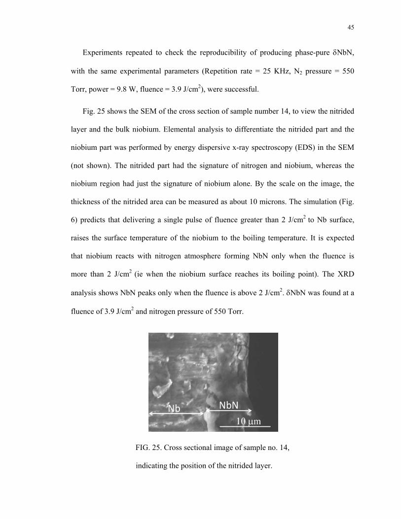
45
Experiments repeated to check the reproducibility of producing phase-pure δNbN,
with the same experimental parameters (Repetition rate = 25 KHz, N2 pressure = 550
Torr, power = 9.8 W, fluence = 3.9 J/cm2), were successful.
Fig. 25 shows the SEM of the cross section of sample number 14, to view the nitrided
layer and the bulk niobium. Elemental analysis to differentiate the nitrided part and the
niobium part was performed by energy dispersive x-ray spectroscopy (EDS) in the SEM
(not shown). The nitrided part had the signature of nitrogen and niobium, whereas the
niobium region had just the signature of niobium alone. By the scale on the image, the
thickness of the nitrided area can be measured as about 10 microns. The simulation (Fig.
6) predicts that delivering a single pulse of fluence greater than 2 J/cm2 to Nb surface,
raises the surface temperature of the niobium to the boiling temperature. It is expected
that niobium reacts with nitrogen atmosphere forming NbN only when the fluence is
more than 2 J/cm2 (ie when the niobium surface reaches its boiling point). The XRD
analysis shows NbN peaks only when the fluence is above 2 J/cm2. δNbN was found at a
fluence of 3.9 J/cm2 and nitrogen pressure of 550 Torr.
FIG. 25. Cross sectional image of sample no. 14,
indicating the position of the nitrided layer.
46
V. CONCLUSION
These results provide evidence of the successful nitriding of niobium to produce a
superconducting niobium nitride (δNbN) surface layer by rapid thermal treatment using a
nanosecond laser. The atomic concentration of N and Nb, did not change drastically with
the change of number of pulse overlap per area. But comparing the surface morphology,
it was clear that a lesser number of pulses overlapping per area produced less roughness
(surface looks smoother), than with a higher number of pulses. The surface temperature
simulation results were consistent with the measured threshold for laser nitriding as
indicated by the NbN peaks detected through the XRD data. The most likely reason for
success in producing phase-pure δNbN compared to previous work is the high cooling
rate that avoided conversion of δNbN to the non-superconducting hexagonal ε phase.
47
CHAPTER 4
PULSED LASER DEPOSITION OF
NbN THIN FILMS
I. INTRODUCTION
At present, the material used in superconducting RF cavities is niobium, with a
critical temperature Tc = 9.2 K. To reach very high accelerating fields (50-100 MV/m),
other materials, having Tc and critical magnetic field higher than niobium, may be
needed. The interest in the materials with a critical temperature higher than niobium is
connected to the relation between Tc and the RF surface electrical resistance (an
exponential function of Tc/T) and to the fact that the accelerating field can be increased,
other factors being equal, as the surface resistance decreases. Therefore, high values of Tc
could allow one to reach higher accelerating fields, or to have reduced the thermal losses
at the same accelerating gradient. Delta phase niobium nitrides are potentially useful
materials for superconducting applications due to their high critical temperature (Tc ≅ 17
K) and to the potentially easy preparation process.81
The niobium nitrides have been well developed as thin films by several methods such
as vacuum arc deposition,82-85 reactive magnetron sputtering,86-92 ion beam assisted
processes,93-95 with an unbalanced magnetron,96 and by pulsed laser deposition.97 Using
different techniques, NbN thin film was deposited on different substrates such as
MgO,97-100 copper,101 niobium,71,102,103 sapphire,81,104 silicon,99 and fused quartz

48
plates.100,105 The properties of the thin films were studied, with the result that mixed
phases of NbN were produced in the thin films.
Using pulsed laser deposition, R.E. Teece, et.al, reported the growth of NbN
superconducting films on a MgO substrate by using a KrF excimer laser (λ = 248nm) in a
10% H2 and 90% N2 background gas.98,106 V. Boffa, et.al.,107 reported producing a NbN
superconducting films on a MgO substrate by using a Nd:YAG laser (λ = 532nm)
deposited in a pure N2 atmosphere. Throughout a literature search no work on depositing
superconducting NbN thin film either on Nb or Cu using pulsed laser deposition with a
pure N2 atmosphere was found. Here I present the initial work performed on depositing
δNbN thin film on a Cu and a Nb substrate in pure N2 atmosphere using a HIPPO
(λ = 1064 nm) and COMPEX Pro 205 excimer laser (λ =248 nm) respectively.
The decision to use a copper substrate was based on the low cost, and simple surface
preparation, as well as a higher thermal conductivity (485W/mK at 4.2 K) compared to
(28W/mK at 4.2 K/RRR = 40) for Nb, which improves heat transfer to the He-bath.108
The risk of quenching is thus greatly reduced and operational safety increased.109
II. EXPERIMENTAL DETAILS
The PVD Products Inc. PLD 5000 (Fig. 26) at Jefferson Lab, and PLD MBE 2000
(Fig. 27) at PVD Products Inc., Boston, were used to carry out the following experiments.
Niobium discs of two different dimensions (50 mm in diameter, 2-3 mm in thickness
and 50 mm in diameter, 6-7 mm in thickness) cut from a reactor grade multigrain
niobium sheet used for SRF cavities were used in two different PLD systems. The
samples were degreased in a detergent with ultrasonic agitation, and buffered chemically
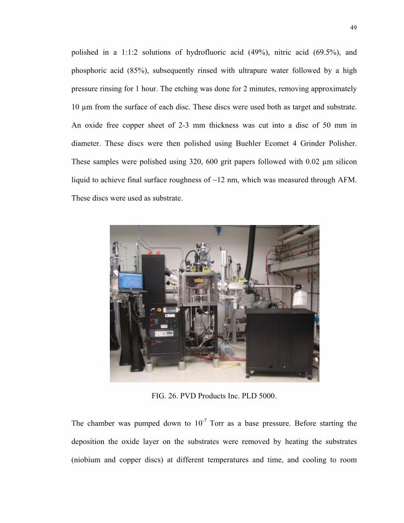
49
polished in a 1:1:2 solutions of hydrofluoric acid (49%), nitric acid (69.5%), and
phosphoric acid (85%), subsequently rinsed with ultrapure water followed by a high
pressure rinsing for 1 hour. The etching was done for 2 minutes, removing approximately
10 µm from the surface of each disc. These discs were used both as target and substrate.
An oxide free copper sheet of 2-3 mm thickness was cut into a disc of 50 mm in
diameter. These discs were then polished using Buehler Ecomet 4 Grinder Polisher.
These samples were polished using 320, 600 grit papers followed with 0.02 µm silicon
liquid to achieve final surface roughness of ~12 nm, which was measured through AFM.
These discs were used as substrate.
FIG. 26. PVD Products Inc. PLD 5000.
The chamber was pumped down to 10-7 Torr as a base pressure. Before starting the
deposition the oxide layer on the substrates were removed by heating the substrates
(niobium and copper discs) at different temperatures and time, and cooling to room
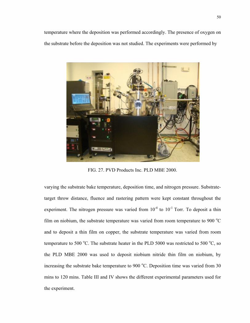
50
temperature where the deposition was performed accordingly. The presence of oxygen on
the substrate before the deposition was not studied. The experiments were performed by
FIG. 27. PVD Products Inc. PLD MBE 2000.
varying the substrate bake temperature, deposition time, and nitrogen pressure. Substrate-
target throw distance, fluence and rastering pattern were kept constant throughout the
experiment. The nitrogen pressure was varied from 10-4 to 10-1 Torr. To deposit a thin
film on niobium, the substrate temperature was varied from room temperature to 900 oC
and to deposit a thin film on copper, the substrate temperature was varied from room
temperature to 500 oC. The substrate heater in the PLD 5000 was restricted to 500 oC, so
the PLD MBE 2000 was used to deposit niobium nitride thin film on niobium, by
increasing the substrate bake temperature to 900 oC. Deposition time was varied from 30
mins to 120 mins. Table III and IV shows the different experimental parameters used for
the experiment.
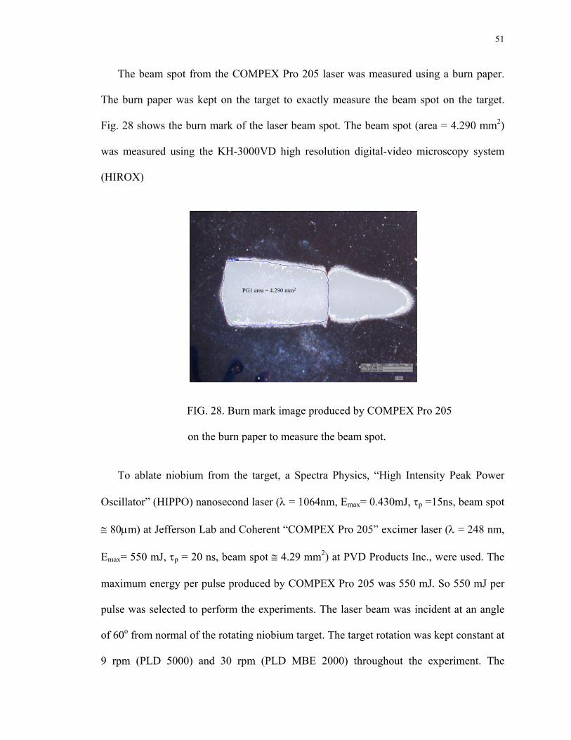
51
The beam spot from the COMPEX Pro 205 laser was measured using a burn paper.
The burn paper was kept on the target to exactly measure the beam spot on the target.
Fig. 28 shows the burn mark of the laser beam spot. The beam spot (area = 4.290 mm2)
was measured using the KH-3000VD high resolution digital-video microscopy system
(HIROX)
FIG. 28. Burn mark image produced by COMPEX Pro 205
on the burn paper to measure the beam spot.
To ablate niobium from the target, a Spectra Physics, “High Intensity Peak Power
Oscillator” (HIPPO) nanosecond laser (λ = 1064nm, Emax= 0.430mJ, τp =15ns, beam spot
≅ 80μm) at Jefferson Lab and Coherent “COMPEX Pro 205” excimer laser (λ = 248 nm,
Emax= 550 mJ, τp = 20 ns, beam spot ≅ 4.29 mm2) at PVD Products Inc., were used. The
maximum energy per pulse produced by COMPEX Pro 205 was 550 mJ. So 550 mJ per
pulse was selected to perform the experiments. The laser beam was incident at an angle
of 60o from normal of the rotating niobium target. The target rotation was kept constant at
9 rpm (PLD 5000) and 30 rpm (PLD MBE 2000) throughout the experiment. The
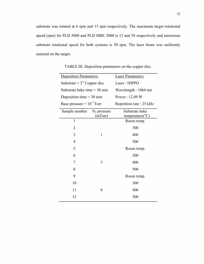
52
substrate was rotated at 6 rpm and 15 rpm respectively. The maximum target rotational
speed (rpm) for PLD 5000 and PLD MBE 2000 is 12 and 50 respectively and maximum
substrate rotational speed for both systems is 50 rpm. The laser beam was uniformly
rastered on the target.
TABLE III. Deposition parameters on the copper disc.
Deposition Parameters:
Substrate = 2” Copper disc
Substrate bake time = 30 min
Deposition time = 30 min
Base pressure = 10-7 Torr
Laser Parameters:
Laser : HIPPO
Wavelength : 1064 nm
Power : 12.09 W
Repetition rate : 25 kHz
Sample number N2 pressure (mTorr)
Substrate bake temperature(oC)
1
1
Room temp.
2 300
3 400
4 500
5
3
Room temp.
6 300
7 400
8 500
9
8
Room temp.
10 300
11 400
12 500
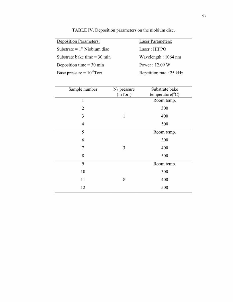
53
TABLE IV. Deposition parameters on the niobium disc.
Deposition Parameters:
Substrate = 1” Niobium disc
Substrate bake time = 30 min
Deposition time = 30 min
Base pressure = 10-7Torr
Laser Parameters:
Laser : HIPPO
Wavelength : 1064 nm
Power : 12.09 W
Repetition rate : 25 kHz
Sample number N2 pressure (mTorr)
Substrate bake temperature(oC)
1
1
Room temp.
2 300
3 400
4 500
5
3
Room temp.
6 300
7 400
8 500
9
8
Room temp.
10 300
11 400
12 500
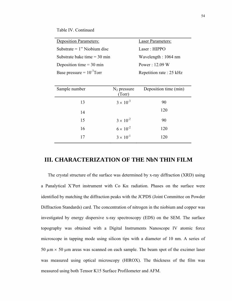
54
Table IV. Continued
Deposition Parameters:
Substrate = 1” Niobium disc
Substrate bake time = 30 min
Deposition time = 30 min
Base pressure = 10-7Torr
Laser Parameters:
Laser : HIPPO
Wavelength : 1064 nm
Power : 12.09 W
Repetition rate : 25 kHz
Sample number N2 pressure (Torr)
Deposition time (min)
13 3 × 10⁻³ 90
14 120
15 3 × 10⁻² 90
16 6 × 10⁻² 120
17 3 × 10⁻¹ 120
III. CHARACTERIZATION OF THE NbN THIN FILM
The crystal structure of the surface was determined by x-ray diffraction (XRD) using
a Panalytical X’Pert instrument with Co Kα radiation. Phases on the surface were
identified by matching the diffraction peaks with the JCPDS (Joint Committee on Powder
Diffraction Standards) card. The concentration of nitrogen in the niobium and copper was
investigated by energy dispersive x-ray spectroscopy (EDS) on the SEM. The surface
topography was obtained with a Digital Instruments Nanoscope IV atomic force
microscope in tapping mode using silicon tips with a diameter of 10 nm. A series of
50 μm × 50 μm areas was scanned on each sample. The beam spot of the excimer laser
was measured using optical microscopy (HIROX). The thickness of the film was
measured using both Tensor K15 Surface Profilometer and AFM.
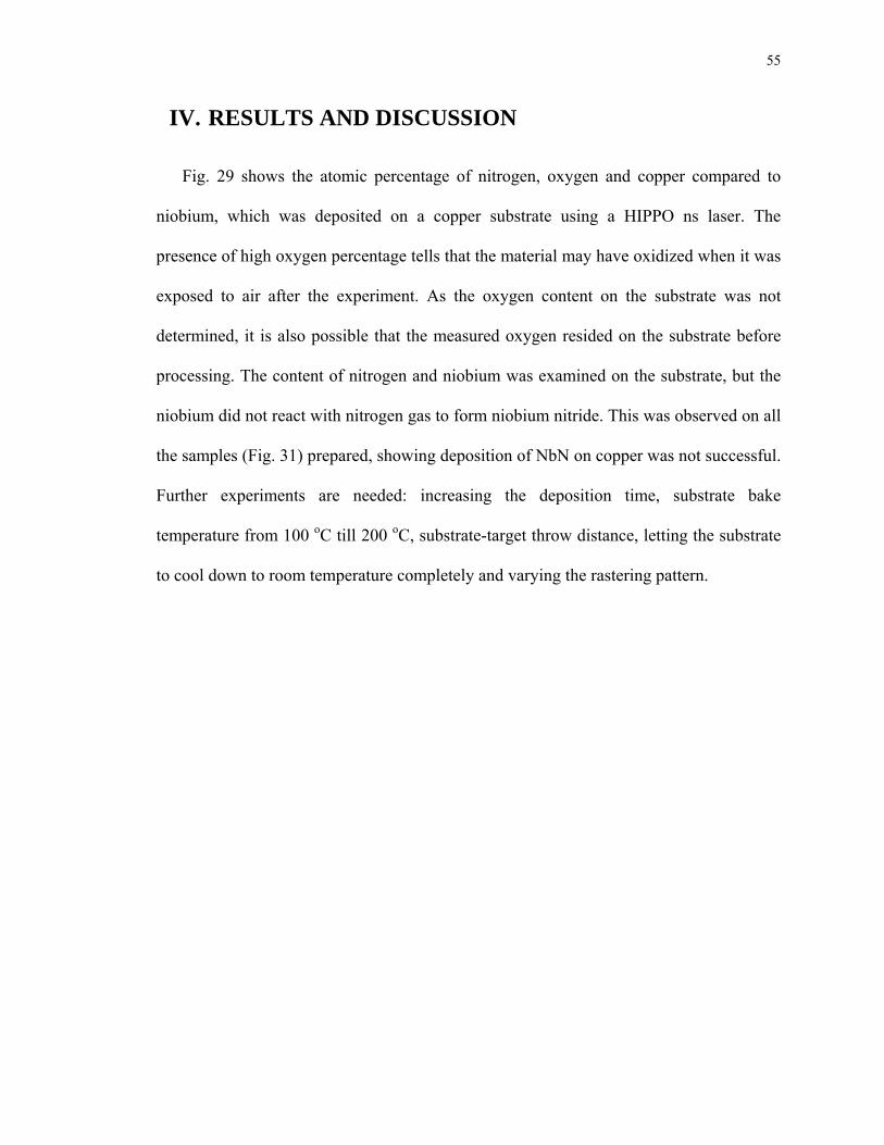
55
IV. RESULTS AND DISCUSSION
Fig. 29 shows the atomic percentage of nitrogen, oxygen and copper compared to
niobium, which was deposited on a copper substrate using a HIPPO ns laser. The
presence of high oxygen percentage tells that the material may have oxidized when it was
exposed to air after the experiment. As the oxygen content on the substrate was not
determined, it is also possible that the measured oxygen resided on the substrate before
processing. The content of nitrogen and niobium was examined on the substrate, but the
niobium did not react with nitrogen gas to form niobium nitride. This was observed on all
the samples (Fig. 31) prepared, showing deposition of NbN on copper was not successful.
Further experiments are needed: increasing the deposition time, substrate bake
temperature from 100 oC till 200 oC, substrate-target throw distance, letting the substrate
to cool down to room temperature completely and varying the rastering pattern.

56
0 1 2 3 4 5 6 7 8 9 10 11 12 130
4
8
12
16
20
24
28
32
36
40
NbN thin film on copper
Ato
mic
per
cent
age
Sample number
N O Nb Cu
FIG. 29. Atomic percentage of various element in the thin film on copper substrate.
Fig. 30 shows the atomic percentage of nitrogen and oxygen compared to niobium which
was deposited on a niobium substrate using both HIPPO and COMPEX Pro 205.
Nitrogen was not observed on the thin films deposited (sample 1- 13) using the ns
HIPPO, providing evidence that niobium nitride could not have been developed in these
samples. Due to the fact that the substrate bake temperature was limited to 500 oC or the
substrate bake time was limited to 30 minutes, the deposition time was not enough to
form NbN thin film on niobium. It is important to further explore these parameters to
observe δNbN on niobium. When the samples (sample number 14-18) were prepared
using COMPEX Pro 205, the ratio of nitrogen to niobium was sufficient to indicate
niobium nitride. This shows evidence that the substrate bake temperature, bake time and
deposition time may be important parameters for forming the niobium nitride thin film.
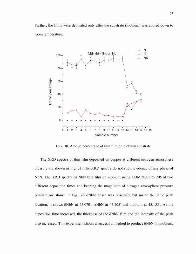
57
Further, the films were deposited only after the substrate (niobium) was cooled down to
room temperature.
0 1 2 3 4 5 6 7 8 9 10 11 12 13 14 15 16 17 18 19
0
20
40
60
80
100
Ato
mic
per
cent
age
Sample number
N O Nb
NbN thin film on Nb
FIG. 30. Atomic percentage of thin film on niobium substrate.
The XRD spectra of thin film deposited on copper at different nitrogen atmosphere
pressure are shown in Fig. 31. The XRD spectra do not show evidence of any phase of
NbN. The XRD spectra of NbN thin film on niobium using COMPEX Pro 205 at two
different deposition times and keeping the magnitude of nitrogen atmosphere pressure
constant are shown in Fig. 32. δNbN phase was observed, but inside the same peak
location, it shows δNbN at 45.070o, αNbN at 45.105o and niobium at 45.155o. As the
deposition time increased, the thickness of the δNbN film and the intensity of the peak
also increased. This experiment shows a successful method to produce δNbN on niobium.
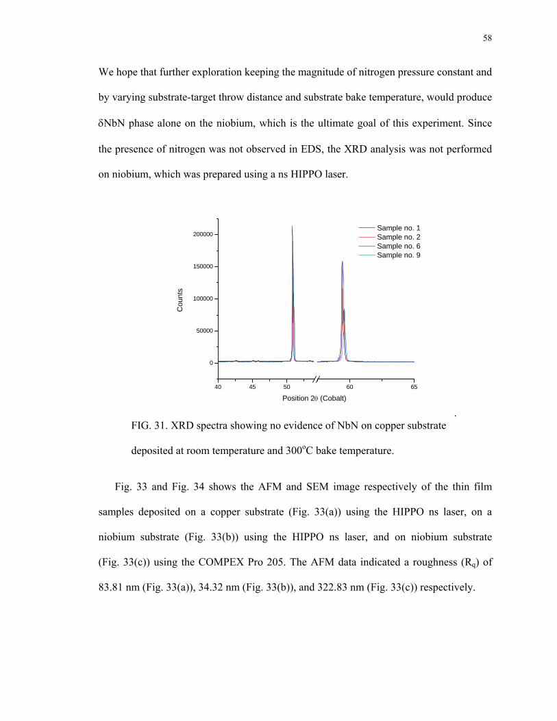
58
We hope that further exploration keeping the magnitude of nitrogen pressure constant and
by varying substrate-target throw distance and substrate bake temperature, would produce
δNbN phase alone on the niobium, which is the ultimate goal of this experiment. Since
the presence of nitrogen was not observed in EDS, the XRD analysis was not performed
on niobium, which was prepared using a ns HIPPO laser.
40 45 50 60 65
0
50000
100000
150000
200000
Cou
nts
Position 2θ (Cobalt)
Sample no. 1 Sample no. 2 Sample no. 6 Sample no. 9
. FIG. 31. XRD spectra showing no evidence of NbN on copper substrate
deposited at room temperature and 300oC bake temperature.
Fig. 33 and Fig. 34 shows the AFM and SEM image respectively of the thin film
samples deposited on a copper substrate (Fig. 33(a)) using the HIPPO ns laser, on a
niobium substrate (Fig. 33(b)) using the HIPPO ns laser, and on niobium substrate
(Fig. 33(c)) using the COMPEX Pro 205. The AFM data indicated a roughness (Rq) of
83.81 nm (Fig. 33(a)), 34.32 nm (Fig. 33(b)), and 322.83 nm (Fig. 33(c)) respectively.

59
40 45 65 70
0
50000
100000
150000
200000
250000
300000
Cou
nts
Position 2θ (Cobalt)
Sample no. 15 Sample no. 16
NbN thin film on niobium @9000C bake
δNbN Nb
FIG. 32. XRD spectra showing the presence of presence of
δNbN, Nb and αNbN on niobium substrate.
FIG. 33. AFM images of (a) Thin film on copper using the HIPPO (sample number 2).
(b)Thin film on niobium using the HIPPO (sample number 6). (c) NbN thin film on
niobium using the excimer laser. (sample number 15).
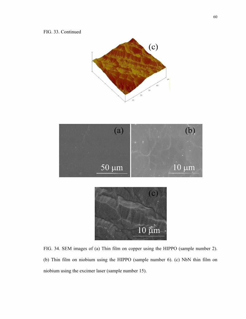
60
FIG. 33. Continued
FIG. 34. SEM images of (a) Thin film on copper using the HIPPO (sample number 2).
(b) Thin film on niobium using the HIPPO (sample number 6). (c) NbN thin film on
niobium using the excimer laser (sample number 15).

61
Fig. 35 shows the thickness measurement obtained using the surface profilometer on
three different thin film samples deposited on: copper substrate (Fig. 35(a)) using the
HIPPO laser, on niobium substrate (Fig. 35(b)) using the HIPPO laser, and a niobium
substrate (Fig. 35(c)) using the COMPEX Pro 205. As the substrate was baked at high
temperature, preparing a step on the surface of the substrate using some mask was not
possible. So the thickness of the thin film was measured near to the edge of the sample,
where it was placed on the substrate holder. Thus a clear step was not observed.
Fig. 35(a) shows the line scan on the edge of the thin film prepared using the HIPPO and
a copper substrate, which gives the average thickness of the thin film of 5-15 nm. A
thickness of 70-95 nm (Fig. 35(b)) was measured on the thin film deposited on niobium
for 90 min using excimer laser and a thickness of 190-260 nm (Fig. 35(c)) on the thin
film deposited on niobium for 120 min using excimer laser. Fig. 36 shows the AFM
image which differentiates the border of the thin film and the substrate, which also shows
that it was not a proper step.
Fig. 37 shows the images of scotch tape measurements for adhesion properties of thin
film on two samples deposited using the COMPEX Pro 205 on a niobium substrate. A
small area on the surface of the sample was scratched in an island formation using a razor
and a scotch tape was adhered and pealed out to see if the thin film from the scratched
area was removed. Fig. 37(a) and 37(c) are the image on the sample 14 and 15 before the
tape was adhered. Fig. 37(b) and 37(d) are the image on the sample after the tape was
removed. As the thin film was not removed from the surface, it shows that the thin film
had good bonding with the substrate
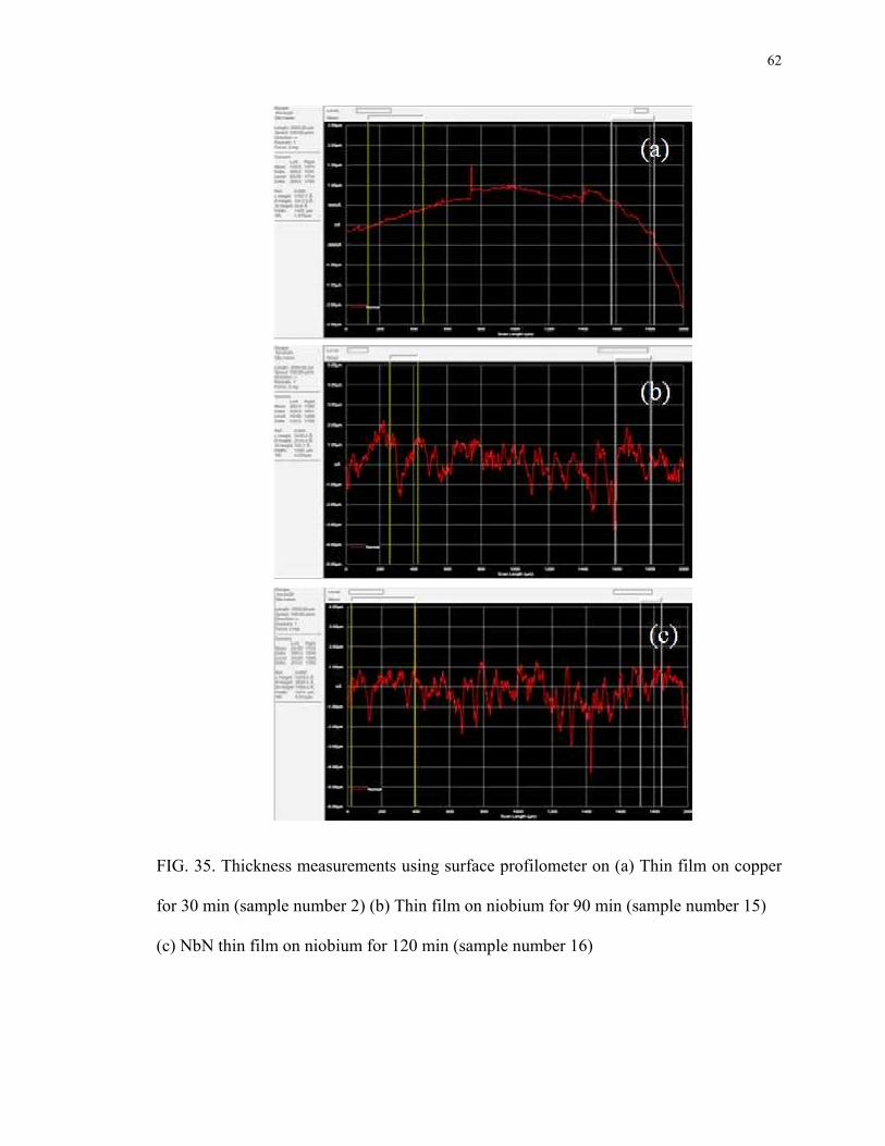
62
FIG. 35. Thickness measurements using surface profilometer on (a) Thin film on copper
for 30 min (sample number 2) (b) Thin film on niobium for 90 min (sample number 15)
(c) NbN thin film on niobium for 120 min (sample number 16)
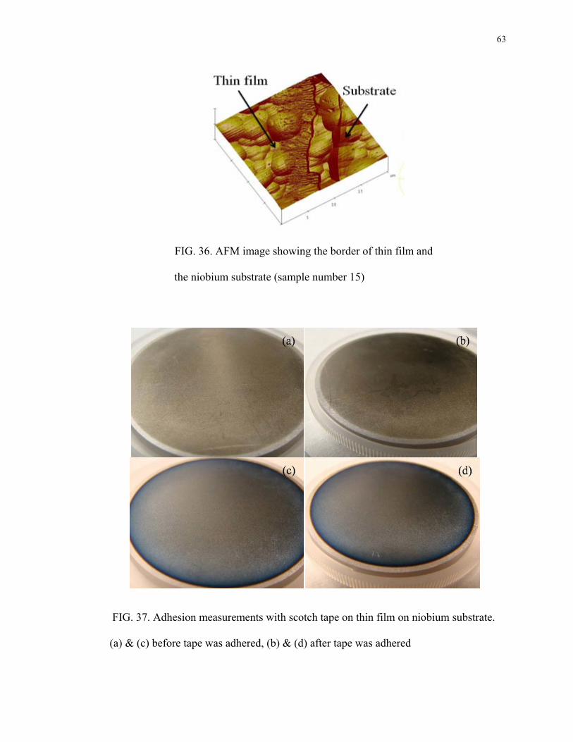
63
FIG. 36. AFM image showing the border of thin film and
the niobium substrate (sample number 15)
FIG. 37. Adhesion measurements with scotch tape on thin film on niobium substrate.
(a) & (c) before tape was adhered, (b) & (d) after tape was adhered
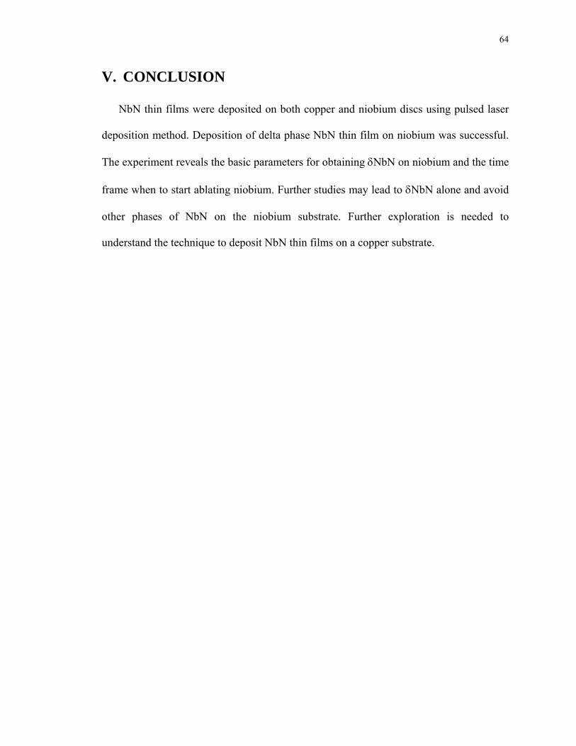
64
V. CONCLUSION
NbN thin films were deposited on both copper and niobium discs using pulsed laser
deposition method. Deposition of delta phase NbN thin film on niobium was successful.
The experiment reveals the basic parameters for obtaining δNbN on niobium and the time
frame when to start ablating niobium. Further studies may lead to δNbN alone and avoid
other phases of NbN on the niobium substrate. Further exploration is needed to
understand the technique to deposit NbN thin films on a copper substrate.
65
CHAPTER 5
RESONANT INFRARED PULSED LASER
DEPOSITION OF CYCLIC OLEFIN
COPOLYMER FILMS
I. INTRODUCTION
Organic polymers are emerging as a class of materials having many possible
applications in electronics and opto-electronics.110 The developments in these devices
such as thin film transistors, polymer light emitting diodes (PLEDs), and organic light
emitting diodes (OLEDs) have highlighted the need for protective and barrier thin films.
The importance of barrier and protective coatings in extending the lifetime and reliability
of OLEDs is well documented.111 The properties of the barrier layers should include
being impervious to water vapor and air through millions of operational cycles over the
lifetime of the devices, and also being optically transparent. A polymer that has recently
attracted considerable interest as a barrier material is cyclic olefin copolymer (COC). The
COC chain consists of ethylene and norbornene, and the glass transition temperature can
be varied from about 75oC to 170oC by changing the ratio between the two monomers.112
Because the bulky cyclic olefin units randomly or alternately attach to the polymer
backbone, the copolymer becomes amorphous and shows the properties of high glass-
transition temperature (Tg) optical clarity, low shrinkage, low moisture absorption, and
low birefringence.113-115 With these properties, the application of cyclic olefin copolymer

66
has now been extended to production of plastic lenses, optical storage media, and also
acts as a barrier material.
Cyclic olefin copolymer is insoluble and thus cannot be deposited by spin coating. A
few attempts have been made to deposit organics and polymers using infrared pulsed
laser deposition.116 Picosecond tunable infrared wavelength lasers were not broadly used
for these applications until 2001.117 Since then, a variety of thermoplastic, thermoset,
conducting and semiconducting polymers has been carried out. Significantly, tunable
infrared laser has been useful to grow thin films of insoluble polymers that are almost
impossible otherwise e.g., polytetrafluoroethylene (Teflon®), 118 polyimide119 and metal
or dielectric nanoparticles.120 Because the mid-infrared photons have energies well below
those required to break the bonds that connect monomer units, resonance infrared laser
irradiation ablates polymers without photo fragmentation, unlike ultraviolet pulsed laser
deposition (UV-PLD).
Here we report on vapor-phase deposition of a barrier and protective polymer, cyclic
olefin copolymer (COC), potentially useful in fabrication of OLEDs by resonant infrared
pulsed laser deposition (RIR-PLD) using the free electron laser (FEL) and compared the
results with those obtained from off-resonant infrared pulsed laser deposition using a
nanosecond high power Q-switched laser, both at Jefferson Laboratory. The deposited
films were characterized by FE-SEM (Hitachi 4700 SEM/EDX), Digital Instruments
Nanoscope IV atomic force microscope, Fourier-transform infrared spectrometry, and
HIROX. Also the ablation fluence threshold of FEL photons on COC was measured.
These experiments give a preliminary indication of the laser parameters needed to make
RIR-PLD deposition of barrier layers of COC a viable commercial process.

67
II. LASERS
Two different laser sources were used in these experiments. The first was the
upgraded Jefferson Lab free-electron laser (FEL), a wavelength-tunable, sub picosecond,
infrared light source offering a combination of high repetition rate and high power per
pulse and capable of delivering average powers in excess of 10 kW.121 The FEL, shown
schematically in Fig. 38(a), is driven by a superconducting energy-recovery linear
accelerator (ERL), a small higher-current relative of the continuous electron beam
accelerator facility (CEBAF) used for nuclear physics. In the ERL, each electron
circulates once rather than being stored for many cycles, as it would in a typical
synchrotron light source. The electron energy is recovered and almost immediately
recycled to a fresh electron in the ERL. The source of the accelerated electron bunches
that produce the laser beam as they pass through the wiggler is a DC electron gun with a
cesiated GaAs photocathode. Because of the nature of the accelerator source, the FEL
produces a continuous stream or bursts of individual pulses, ranging in duration from 0.5
to 5 ps, at pulse repetition rates ranging from 4.5 to 75 MHz. Since operating
continuously at these repetition rates would eventually lead to unacceptable thermal
loading and damage to the ablation targets, a macropulse structure was used to deliver
bursts of pulses from the FEL. Typical bursts (macropulses) ranged from 50 to 250 μs.
Fig. 38(b) shows the pulse structure of the FEL beam used in our experiments.
The second laser used was a Spectra Physics, High Intensity Peak Power Oscillator
(HIPPO), nanosecond high power Q-switched laser system at Jefferson Lab. Table V
shows the specification of the laser system used for our experiment.
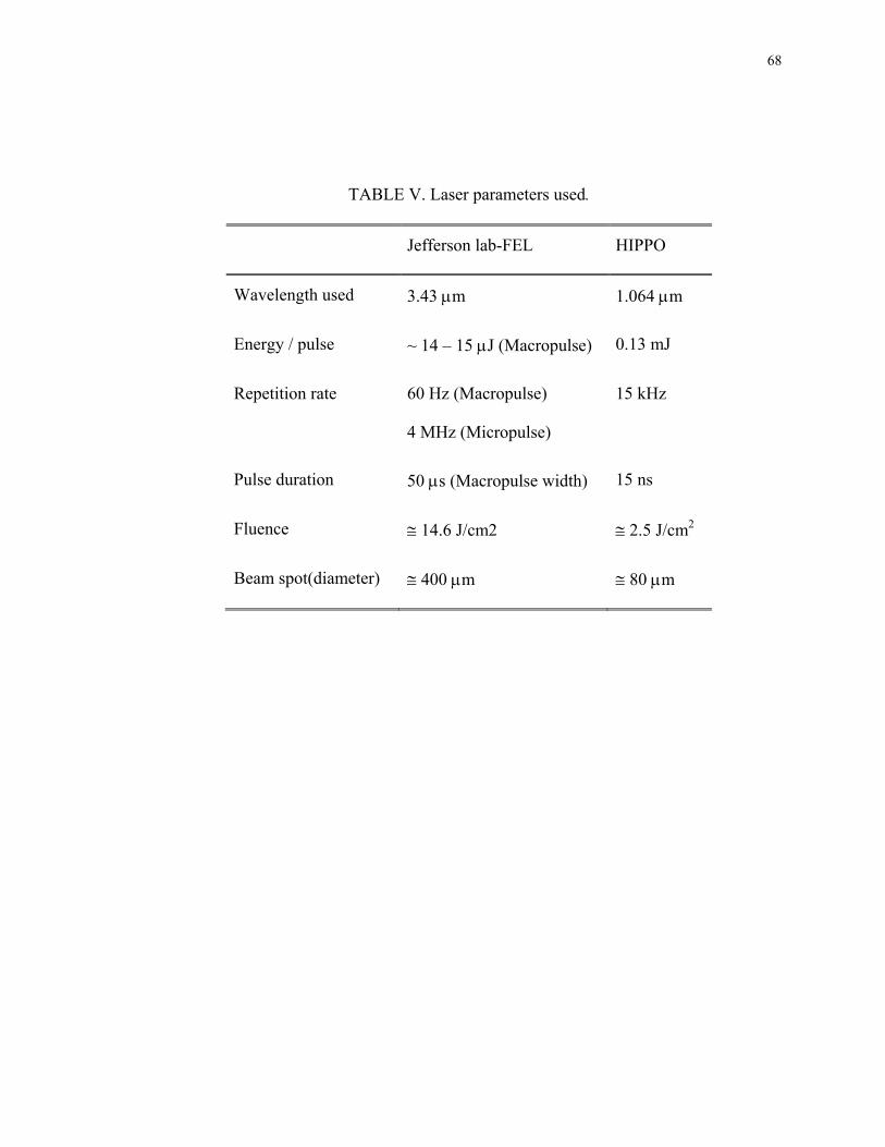
68
TABLE V. Laser parameters used.
Jefferson lab-FEL HIPPO
Wavelength used 3.43 μm 1.064 μm
Energy / pulse ~ 14 – 15 μJ (Macropulse) 0.13 mJ
Repetition rate 60 Hz (Macropulse)
4 MHz (Micropulse)
15 kHz
Pulse duration 50 μs (Macropulse width) 15 ns
Fluence ≅ 14.6 J/cm2 ≅ 2.5 J/cm2
Beam spot(diameter) ≅ 400 μm ≅ 80 μm

69
Fig. 38. (a) Schematic layout of the free-electron laser at the Thomas Jefferson National
Accelerator Laboratory, showing the photocathode electron source and injector, the
superconducting RF linac, the recirculation and energy-recovery arc, and the optical
cavity and wiggler that generates the tunable infrared laser radiation. (b) Pulse structure
of the FEL beam.
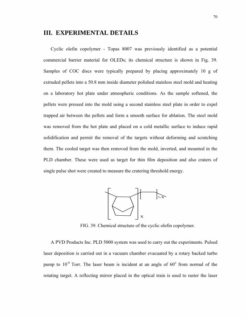
70
III. EXPERIMENTAL DETAILS
Cyclic olefin copolymer - Topas 8007 was previously identified as a potential
commercial barrier material for OLEDs; its chemical structure is shown in Fig. 39.
Samples of COC discs were typically prepared by placing approximately 10 g of
extruded pellets into a 50.8 mm inside diameter polished stainless steel mold and heating
on a laboratory hot plate under atmospheric conditions. As the sample softened, the
pellets were pressed into the mold using a second stainless steel plate in order to expel
trapped air between the pellets and form a smooth surface for ablation. The steel mold
was removed from the hot plate and placed on a cold metallic surface to induce rapid
solidification and permit the removal of the targets without deforming and scratching
them. The cooled target was then removed from the mold, inverted, and mounted in the
PLD chamber. These were used as target for thin film deposition and also craters of
single pulse shot were created to measure the cratering threshold energy.
FIG. 39. Chemical structure of the cyclic olefin copolymer.
A PVD Products Inc. PLD 5000 system was used to carry out the experiments. Pulsed
laser deposition is carried out in a vacuum chamber evacuated by a rotary backed turbo
pump to 10-6 Torr. The laser beam is incident at an angle of 60o from normal of the
rotating target. A reflecting mirror placed in the optical train is used to raster the laser
71
beam over a radial range on the target up to ~ 4.5 cm. The target pedestals can hold the
targets of 50 mm in diameter and 2-3 mm in thickness and can rotate individually with
the maximum rotation speed of 12 rpm. The distance between the substrate (glass slide or
13 mm NaCl disc mounted on the glass slide) and the target was fixed to 10 cm.
The FEL and HIPPO lasers were focused onto the surface of the drop-cast ablation
targets by long focal-length BaF2 lenses. The FEL pulsed beam was focused on one area
on the surface of the target and the target was rotated such that the beam creates a 3 cm
diameter circular track at a rate of either 1 rpm or 5 rpm, exposing the FEL for one
minute. Thus each spot irradiated by the laser in fact absorbs the laser light from
thousands of ps micropulses. The off resonant HIPPO laser was programmed to raster on
the whole target surface, while the target was rotating at a rate of 9 rpm for 10 minutes.
Knife edge measurements were used to determine the beam spot (diameter) for both
FEL and HIPPO lasers (for details see Appendix A). The beam was measured both
vertically and horizontally on the target. To find the ablation threshold of energy
(fluence) per pulse on COC, the FEL beam was delivered to the target in a circular
pattern with a low repetition rate of 1 Hz so that individual spots (craters) on the COC
target could be measured.
IV. RESULTS AND DISCUSSION
Structural and surface topography analysis techniques were used to elucidate the
characteristics of the COC barrier thin film deposited on the NaCl disc using both
resonant and off resonant infrared pulsed laser beams. The COC thin films of thickness
400 nm to 800 nm were successfully deposited using the Jefferson Lab FEL beam at 3.43
μm laser wavelength.
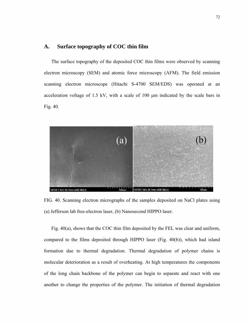
72
A. Surface topography of COC thin film
The surface topography of the deposited COC thin films were observed by scanning
electron microscopy (SEM) and atomic force microscopy (AFM). The field emission
scanning electron microscope (Hitachi S-4700 SEM/EDS) was operated at an
acceleration voltage of 1.5 kV, with a scale of 100 μm indicated by the scale bars in
Fig. 40.
FIG. 40. Scanning electron micrographs of the samples deposited on NaCl plates using
(a) Jefferson lab free-electron laser, (b) Nanosecond HIPPO laser.
Fig. 40(a), shows that the COC thin film deposited by the FEL was clear and uniform,
compared to the films deposited through HIPPO laser (Fig. 40(b)), which had island
formation due to thermal degradation. Thermal degradation of polymer chains is
molecular deterioration as a result of overheating. At high temperatures the components
of the long chain backbone of the polymer can begin to separate and react with one
another to change the properties of the polymer. The initiation of thermal degradation
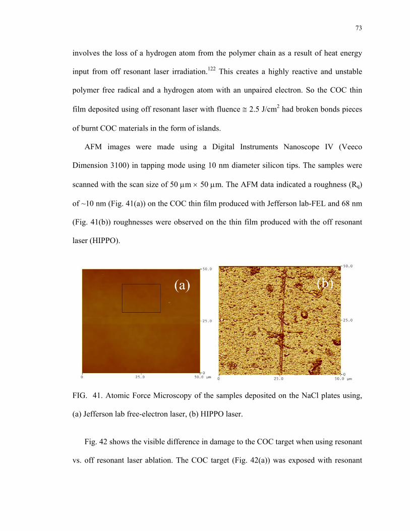
73
involves the loss of a hydrogen atom from the polymer chain as a result of heat energy
input from off resonant laser irradiation.122 This creates a highly reactive and unstable
polymer free radical and a hydrogen atom with an unpaired electron. So the COC thin
film deposited using off resonant laser with fluence ≅ 2.5 J/cm2 had broken bonds pieces
of burnt COC materials in the form of islands.
AFM images were made using a Digital Instruments Nanoscope IV (Veeco
Dimension 3100) in tapping mode using 10 nm diameter silicon tips. The samples were
scanned with the scan size of 50 μm × 50 μm. The AFM data indicated a roughness (Rq)
of ~10 nm (Fig. 41(a)) on the COC thin film produced with Jefferson lab-FEL and 68 nm
(Fig. 41(b)) roughnesses were observed on the thin film produced with the off resonant
laser (HIPPO).
FIG. 41. Atomic Force Microscopy of the samples deposited on the NaCl plates using,
(a) Jefferson lab free-electron laser, (b) HIPPO laser.
Fig. 42 shows the visible difference in damage to the COC target when using resonant
vs. off resonant laser ablation. The COC target (Fig. 42(a)) was exposed with resonant

74
FEL laser at 3.43 microns, where the whole polymer chain was ablated without breaking
the bonds and burning the target.123 Fig. 42(b), shows the thermal degradation on the
surface of the COC target after exposing it to an off resonant wavelength (1.064
microns), indicating the breaking of bonds due to thermal energy produced at this
wavelength. These characterizations also show that RIR-PLD reduces polymer damage
by tuning an infrared laser wavelength to a specific bond stretch or bond bend vibrational
absorption peaks of the starting material, proving that wavelength is an important
parameter for polymer thin film deposition.
Also another parameter to be noted is fluence. Though the fluence of the off resonant
laser was very low compared to the resonant laser source, it has caused thermal damage
on the surface. This shows that a laser source with resonant wavelength and minimum
fluence is capable to ablate polymer chain to deposit polymer thin film. So finding the
ablation threshold fluence becomes another important parameter.
FIG. 42. Optical image of the target exposed with (a) FEL and (b) HIPPO lasers

75
B. Stylus Profilometry of deposited COC films
To look at the long-range surface properties of the COC thin films, we used a stylus
Profilometer (Dektak) to scan over the films deposited on the glass substrate. The
deposited COC thin film using the FEL was very clear and transparent. The surface of the
thin film was carefully scratched with a razor blade such that it does not it does not
damage the substrate. This scratch on the thin film was used to measure the thickness of
the thin film.
Fig. 43(a) shows the result of the film scanned over the scratch in the surface of the
COC film, indicating the thickness of the deposited film, as well as surface scans over
comparable stretches of the COC films deposited (fluence of ~14.6 J/cm2). Fig. 45(b)
shows the results of an edge scan for the COC thin film deposited using off resonant
HIPPO laser. The average step height measured on the film to the substrate was ~750 nm
and ~100 μm deposited with the Jefferson lab FEL and the HIPPO laser respectively. The
scanning data obtained in between 500 microns to 2000 microns position from Fig. 43(a)
also indicates that the thin film deposited using FEL beams at 3.43 microns had a uniform
deposition of COC thin films compared with off resonant laser at 1.064 microns (position
0 microns to 350 microns).
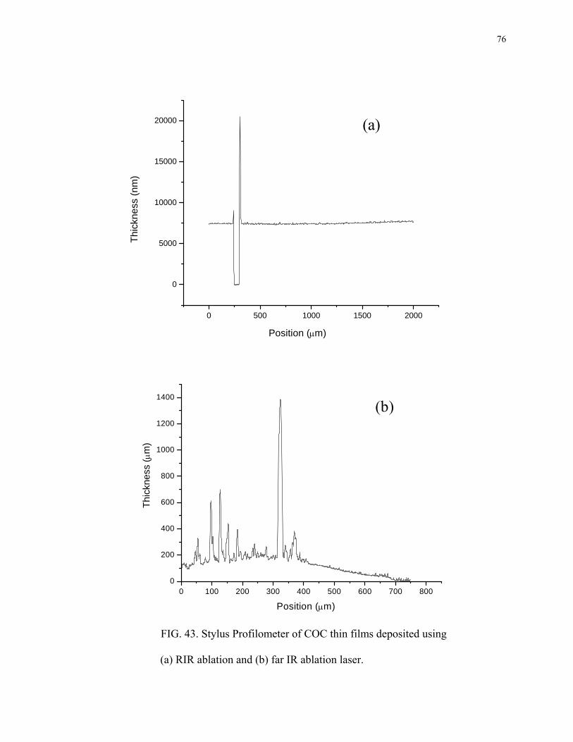
76
0 500 1000 1500 2000
0
5000
10000
15000
20000
Thic
knes
s (n
m)
Position (μm)
(a)
0 100 200 300 400 500 600 700 8000
200
400
600
800
1000
1200
1400
Thic
knes
s (μ
m)
Position (μm)
(b)
FIG. 43. Stylus Profilometer of COC thin films deposited using
(a) RIR ablation and (b) far IR ablation laser.

77
C. FT-IR spectra of COC
Fourier-transform infrared (FTIR) spectrometry is a useful indicator of the extent to
which the anharmonic monomer mode structure of the polymers is intact following laser
ablation. Thus a comparison of the FTIR spectra of bulk sample materials with FTIR
spectra of the deposited films is one indication of whether or not the polymers have
survived more or less undamaged the processes of laser ablation and deposition in the
form of thin films.
To facilitate FTIR measurements, films were deposited onto IR transparent NaCl
plates of 13 mm in diameter and 2 mm in thickness for subsequent analysis. Fig. 44(a),
shows a comparison of the FTIR spectra of FEL and HIPPO laser deposited COC thin
films and a bulk COC disc. The bulk COC measurements of absorption were performed
in reflection configuration and the thin film was analyzed in transmission configuration,
accounting for the different normalization in the curves. The measured spectrum of FEL
deposited COC thin film shows the gross features of bulk COC.

78
2.4 2.8 3.2 3.6 4.0 4.4 4.8 5.2 5.6 6.0
A
bsor
ptio
n
Wavelength (μm)
HIPPO (1.064 μm) Jlab-FEL (3.43 μm) Bulk COC
(a)
3.30 3.35 3.40 3.45 3.50 3.55
Ab
sorp
tion
Wavelength (μm)
HIPPO (1.064 μm) Jlab-FEL (3.43 μm) Bulk COC
(b)
FIG. 44. Measured FTIR spectra (a) Comparing laser deposited thin films and
bulk COC target, and (b) Expansion of FTIR spectra. (c) Measured FEL spectrum
during experiment showing tuned peak at 3.41 μm and FWHM width of 75 nm.
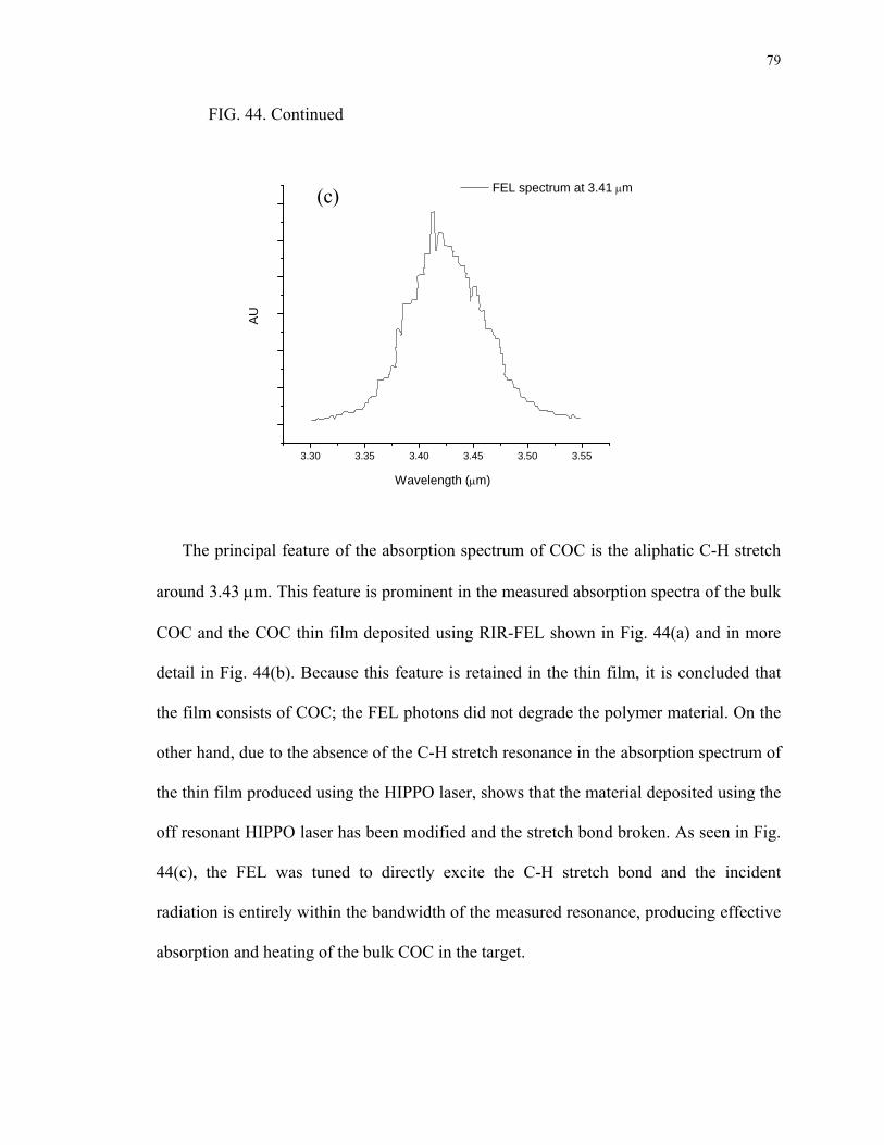
79
FIG. 44. Continued
3.30 3.35 3.40 3.45 3.50 3.55
Wavelength (μm)
AU
FEL spectrum at 3.41 μm(c)
The principal feature of the absorption spectrum of COC is the aliphatic C-H stretch
around 3.43 μm. This feature is prominent in the measured absorption spectra of the bulk
COC and the COC thin film deposited using RIR-FEL shown in Fig. 44(a) and in more
detail in Fig. 44(b). Because this feature is retained in the thin film, it is concluded that
the film consists of COC; the FEL photons did not degrade the polymer material. On the
other hand, due to the absence of the C-H stretch resonance in the absorption spectrum of
the thin film produced using the HIPPO laser, shows that the material deposited using the
off resonant HIPPO laser has been modified and the stretch bond broken. As seen in Fig.
44(c), the FEL was tuned to directly excite the C-H stretch bond and the incident
radiation is entirely within the bandwidth of the measured resonance, producing effective
absorption and heating of the bulk COC in the target.
80
The FEL photon pulse width was not measured during the experiment, but Happek
scans were performed to analyze the electron bunch length which was around 200 fs.
Direct autocorrelation measurements of the FEL photon pulse width could be useful to
understand more clearly what happens on the polymer, when FEL beam at a specific
wavelength and pulse width is irradiated.
D. Erosion of the COC surface due to RIR irradiation followed by
crater depth analysis.
From Fig. 40 to Fig. 44, it was clear that deposition of COC thin films using 3.43
microns IR-FEL at a fluence of ~14.6 J/cm2 was successful. The next important
parameter to be determined was the ablation fluence threshold at the same wavelength.
These individual craters were generated on the clear 50 mm COC target with RIR-FEL
pulse beam with repetition rate of 1 Hz and rotating the COC target, such that the craters
are produced in the circular formation and two exposed areas do not overlap each other.
The depth of the exposed area/crater was measured using 3D optical microscopy
(“HIROX” KH-3000VD high resolution digital-video microscopy system). The
difference between the bottom of the crater and the top surface was scanned layer by
layer (z stack). Fig. 45 shows the evolution of the surface of the COC due to the thermal
energy produced at different fluences. At fluences below ~ 5.5 J/cm2 (Fig. 45(a) – 45(b)),
only surface melting is observed. Above ~5.5 J/cm2 (Fig. 45(c) – 45(f)), the fluences
were sufficient for crater formation. A fluence of ~5.5 J/cm2 is the ablation threshold
fluence of the pulsed FEL beam at 3.43 microns. Though the craters were formed with
depth of ~ 7 microns, the energy was not quite enough to push the material upwards to
reach the substrate which was kept ~10 cm above the target. Further above ~10 J/cm2
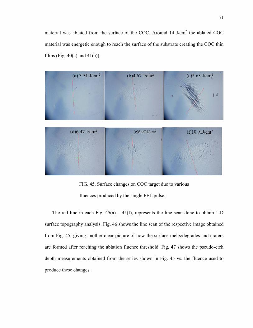
81
material was ablated from the surface of the COC. Around 14 J/cm2 the ablated COC
material was energetic enough to reach the surface of the substrate creating the COC thin
films (Fig. 40(a) and 41(a)).
FIG. 45. Surface changes on COC target due to various
fluences produced by the single FEL pulse.
The red line in each Fig. 45(a) – 45(f), represents the line scan done to obtain 1-D
surface topography analysis. Fig. 46 shows the line scan of the respective image obtained
from Fig. 45, giving another clear picture of how the surface melts/degrades and craters
are formed after reaching the ablation fluence threshold. Fig. 47 shows the pseudo-etch
depth measurements obtained from the series shown in Fig. 45 vs. the fluence used to
produce these changes.

82
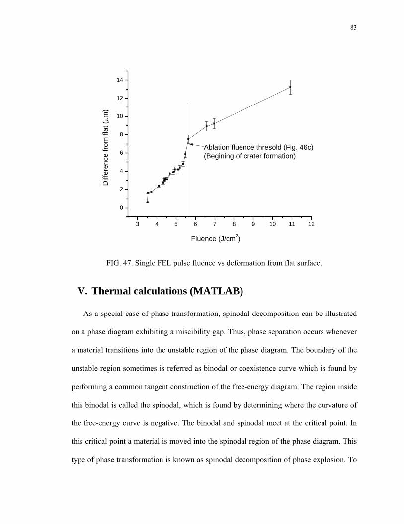
83
3 4 5 6 7 8 9 10 11 12
0
2
4
6
8
10
12
14
Diff
eren
ce fr
om fl
at (μ
m)
Fluence (J/cm2)
Ablation fluence thresold (Fig. 46c)(Begining of crater formation)
FIG. 47. Single FEL pulse fluence vs deformation from flat surface.
V. Thermal calculations (MATLAB)
As a special case of phase transformation, spinodal decomposition can be illustrated
on a phase diagram exhibiting a miscibility gap. Thus, phase separation occurs whenever
a material transitions into the unstable region of the phase diagram. The boundary of the
unstable region sometimes is referred as binodal or coexistence curve which is found by
performing a common tangent construction of the free-energy diagram. The region inside
this binodal is called the spinodal, which is found by determining where the curvature of
the free-energy curve is negative. The binodal and spinodal meet at the critical point. In
this critical point a material is moved into the spinodal region of the phase diagram. This
type of phase transformation is known as spinodal decomposition of phase explosion. To
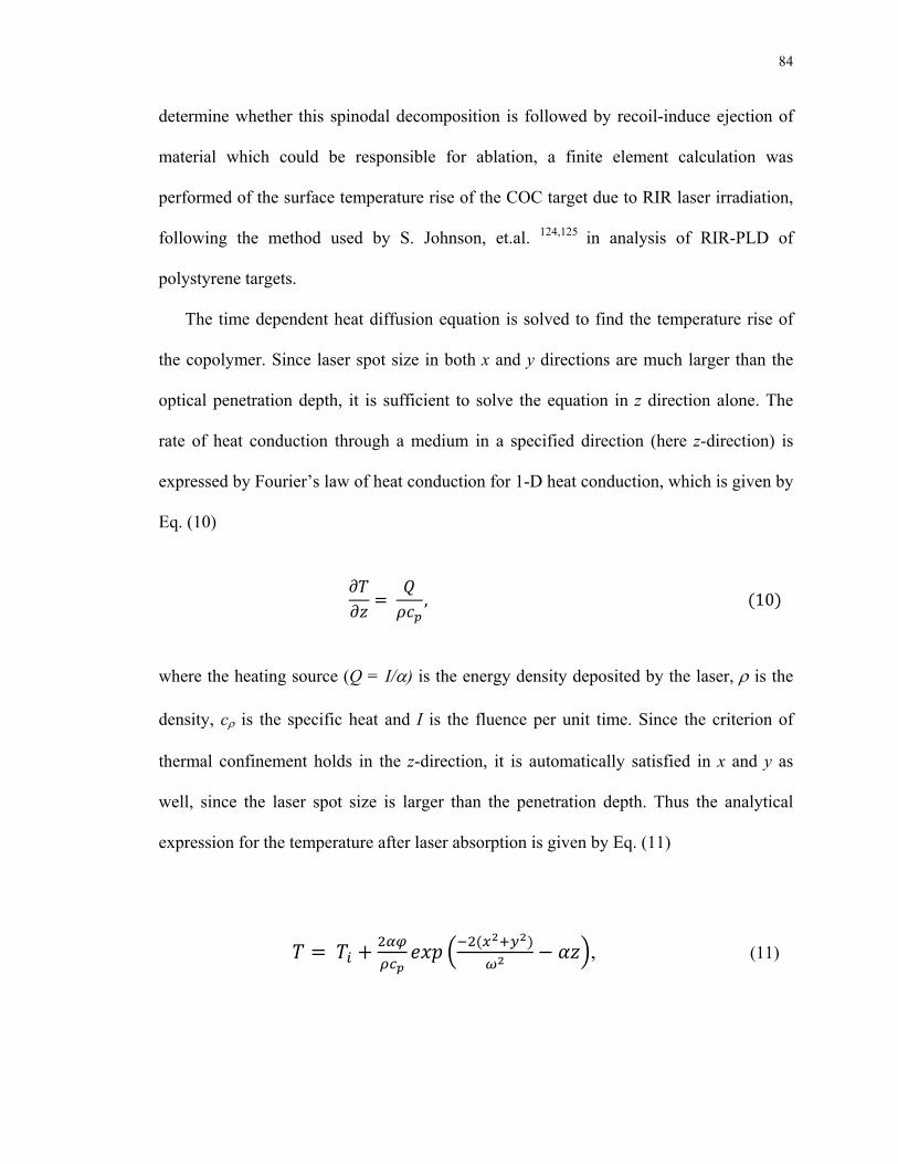
84
determine whether this spinodal decomposition is followed by recoil-induce ejection of
material which could be responsible for ablation, a finite element calculation was
performed of the surface temperature rise of the COC target due to RIR laser irradiation,
following the method used by S. Johnson, et.al. 124,125 in analysis of RIR-PLD of
polystyrene targets.
The time dependent heat diffusion equation is solved to find the temperature rise of
the copolymer. Since laser spot size in both x and y directions are much larger than the
optical penetration depth, it is sufficient to solve the equation in z direction alone. The
rate of heat conduction through a medium in a specified direction (here z-direction) is
expressed by Fourier’s law of heat conduction for 1-D heat conduction, which is given by
Eq. (10)
, 10
where the heating source (Q = I/α) is the energy density deposited by the laser, ρ is the
density, cρ is the specific heat and I is the fluence per unit time. Since the criterion of
thermal confinement holds in the z-direction, it is automatically satisfied in x and y as
well, since the laser spot size is larger than the penetration depth. Thus the analytical
expression for the temperature after laser absorption is given by Eq. (11)
, (11)
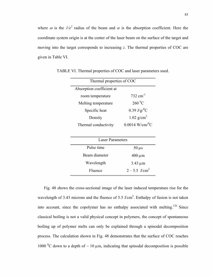
85
where ω is the 1/e2 radius of the beam and α is the absorption coefficient. Here the
coordinate system origin is at the center of the laser beam on the surface of the target and
moving into the target corresponds to increasing z. The thermal properties of COC are
given in Table VI.
TABLE VI. Thermal properties of COC and laser parameters used.
Thermal properties of COC
Absorption coefficient at
room temperature
732 cm-1
Melting temperature 260 0C
Specific heat 0.39 J/g/0C
Density 1.02 g/cm3
Thermal conductivity 0.0014 W/cm/0C
Laser Parameters
Pulse time 50 μs
Beam diameter 400 μm
Wavelength 3.43 μm
Fluence 2 – 5.5 J/cm2
Fig. 48 shows the cross-sectional image of the laser induced temperature rise for the
wavelength of 3.43 microns and the fluence of 5.5 J/cm2. Enthalpy of fusion is not taken
into account, since the copolymer has no enthalpy associated with melting.126 Since
classical boiling is not a valid physical concept in polymers, the concept of spontaneous
boiling up of polymer melts can only be explained through a spinodal decomposition
process. The calculation shown in Fig. 48 demonstrates that the surface of COC reaches
1000 0C down to a depth of ~ 10 μm, indicating that spinodal decomposition is possible
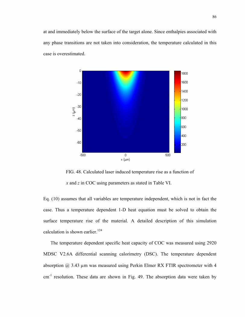
86
at and immediately below the surface of the target alone. Since enthalpies associated with
any phase transitions are not taken into consideration, the temperature calculated in this
case is overestimated.
FIG. 48. Calculated laser induced temperature rise as a function of
x and z in COC using parameters as stated in Table VI.
Eq. (10) assumes that all variables are temperature independent, which is not in fact the
case. Thus a temperature dependent 1-D heat equation must be solved to obtain the
surface temperature rise of the material. A detailed description of this simulation
calculation is shown earlier.124
The temperature dependent specific heat capacity of COC was measured using 2920
MDSC V2.6A differential scanning calorimetry (DSC). The temperature dependent
absorption @ 3.43 μm was measured using Perkin Elmer RX FTIR spectrometer with 4
cm-1 resolution. These data are shown in Fig. 49. The absorption data were taken by
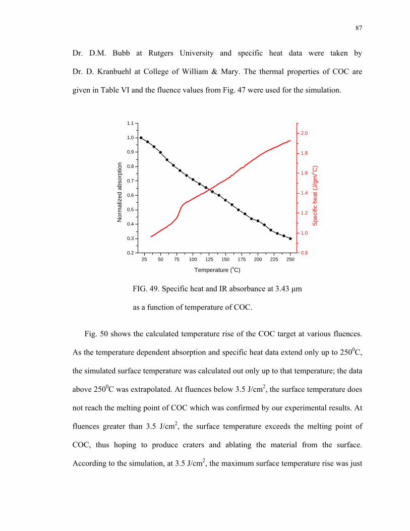
87
Dr. D.M. Bubb at Rutgers University and specific heat data were taken by
Dr. D. Kranbuehl at College of William & Mary. The thermal properties of COC are
given in Table VI and the fluence values from Fig. 47 were used for the simulation.
25 50 75 100 125 150 175 200 225 2500.2
0.3
0.4
0.5
0.6
0.7
0.8
0.9
1.0
1.1
Temperature (oC)
Nor
mal
ized
abs
orpt
ion
0.8
1.0
1.2
1.4
1.6
1.8
2.0
Spec
ific
heat
(J/g
m/o C
)
FIG. 49. Specific heat and IR absorbance at 3.43 μm
as a function of temperature of COC.
Fig. 50 shows the calculated temperature rise of the COC target at various fluences.
As the temperature dependent absorption and specific heat data extend only up to 2500C,
the simulated surface temperature was calculated out only up to that temperature; the data
above 2500C was extrapolated. At fluences below 3.5 J/cm2, the surface temperature does
not reach the melting point of COC which was confirmed by our experimental results. At
fluences greater than 3.5 J/cm2, the surface temperature exceeds the melting point of
COC, thus hoping to produce craters and ablating the material from the surface.
According to the simulation, at 3.5 J/cm2, the maximum surface temperature rise was just
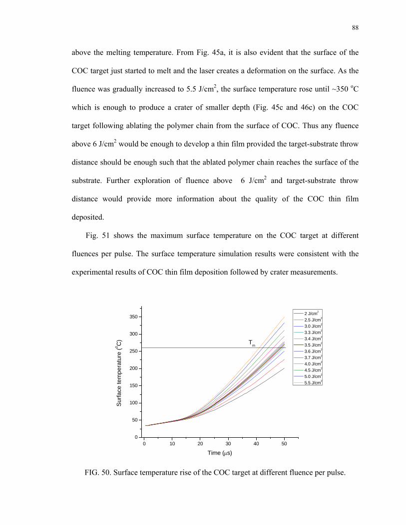
88
above the melting temperature. From Fig. 45a, it is also evident that the surface of the
COC target just started to melt and the laser creates a deformation on the surface. As the
fluence was gradually increased to 5.5 J/cm2, the surface temperature rose until ~350 oC
which is enough to produce a crater of smaller depth (Fig. 45c and 46c) on the COC
target following ablating the polymer chain from the surface of COC. Thus any fluence
above 6 J/cm2 would be enough to develop a thin film provided the target-substrate throw
distance should be enough such that the ablated polymer chain reaches the surface of the
substrate. Further exploration of fluence above 6 J/cm2 and target-substrate throw
distance would provide more information about the quality of the COC thin film
deposited.
Fig. 51 shows the maximum surface temperature on the COC target at different
fluences per pulse. The surface temperature simulation results were consistent with the
experimental results of COC thin film deposition followed by crater measurements.
0 10 20 30 40 500
50
100
150
200
250
300
350
Tm
2 J/cm2
2.5 J/cm2
3.0 J/cm2
3.3 J/cm2
3.4 J/cm2
3.5 J/cm2
3.6 J/cm2
3.7 J/cm2
4.0 J/cm2
4.5 J/cm2
5.0 J/cm2
5.5 J/cm2
Sur
face
tem
pera
ture
(0 C)
Time (μs)
FIG. 50. Surface temperature rise of the COC target at different fluence per pulse.
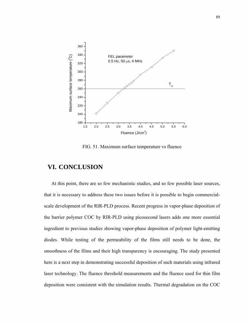
89
1.5 2.0 2.5 3.0 3.5 4.0 4.5 5.0 5.5 6.0180
200
220
240
260
280
300
320
340
360
Tm
FEL parameter0.5 Hz, 50 μs, 4 MHz
Fluence (J/cm2)
Max
imum
sur
face
tem
pera
ture
(0 C)
FIG. 51. Maximum surface temperature vs fluence
VI. CONCLUSION
At this point, there are so few mechanistic studies, and so few possible laser sources,
that it is necessary to address these two issues before it is possible to begin commercial-
scale development of the RIR-PLD process. Recent progress in vapor-phase deposition of
the barrier polymer COC by RIR-PLD using picosecond lasers adds one more essential
ingredient to previous studies showing vapor-phase deposition of polymer light-emitting
diodes. While testing of the permeability of the films still needs to be done, the
smoothness of the films and their high transparency is encouraging. The study presented
here is a next step in demonstrating successful deposition of such materials using infrared
laser technology. The fluence threshold measurements and the fluence used for thin film
deposition were consistent with the simulation results. Thermal degradation on the COC

90
surface using an off resonant wavelength laser was observed, which proves wavelength is
an important parameter polymer thin film deposition. Continued development of
appropriate picosecond sources for the mid-infrared remains a high priority in order to
develop this branch of thin-film synthesis for the future of organic and polymer-based
optoelectronic devices.
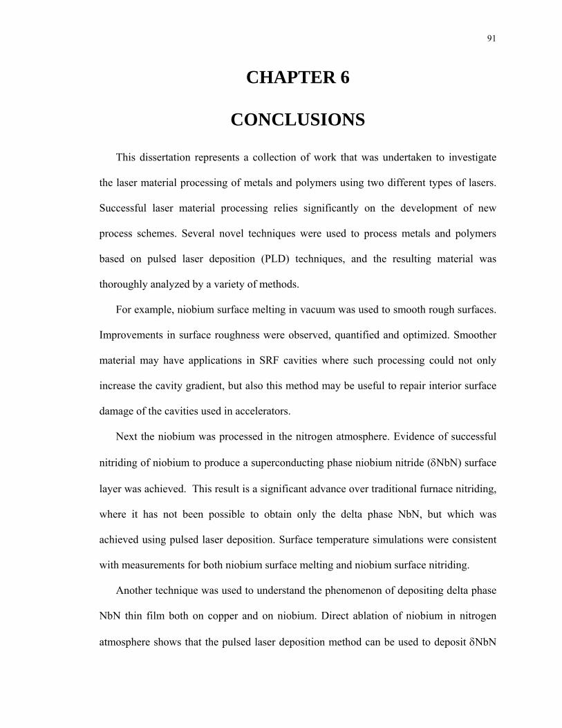
91
CHAPTER 6
CONCLUSIONS
This dissertation represents a collection of work that was undertaken to investigate
the laser material processing of metals and polymers using two different types of lasers.
Successful laser material processing relies significantly on the development of new
process schemes. Several novel techniques were used to process metals and polymers
based on pulsed laser deposition (PLD) techniques, and the resulting material was
thoroughly analyzed by a variety of methods.
For example, niobium surface melting in vacuum was used to smooth rough surfaces.
Improvements in surface roughness were observed, quantified and optimized. Smoother
material may have applications in SRF cavities where such processing could not only
increase the cavity gradient, but also this method may be useful to repair interior surface
damage of the cavities used in accelerators.
Next the niobium was processed in the nitrogen atmosphere. Evidence of successful
nitriding of niobium to produce a superconducting phase niobium nitride (δNbN) surface
layer was achieved. This result is a significant advance over traditional furnace nitriding,
where it has not been possible to obtain only the delta phase NbN, but which was
achieved using pulsed laser deposition. Surface temperature simulations were consistent
with measurements for both niobium surface melting and niobium surface nitriding.
Another technique was used to understand the phenomenon of depositing delta phase
NbN thin film both on copper and on niobium. Direct ablation of niobium in nitrogen
atmosphere shows that the pulsed laser deposition method can be used to deposit δNbN
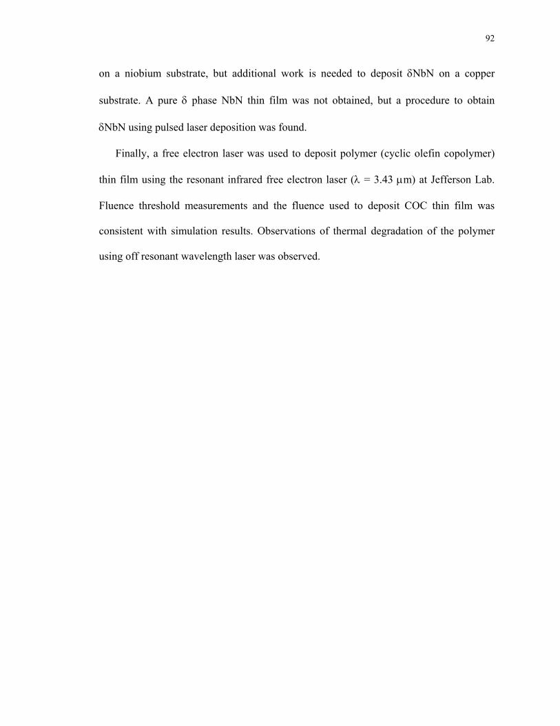
92
on a niobium substrate, but additional work is needed to deposit δNbN on a copper
substrate. A pure δ phase NbN thin film was not obtained, but a procedure to obtain
δNbN using pulsed laser deposition was found.
Finally, a free electron laser was used to deposit polymer (cyclic olefin copolymer)
thin film using the resonant infrared free electron laser (λ = 3.43 μm) at Jefferson Lab.
Fluence threshold measurements and the fluence used to deposit COC thin film was
consistent with simulation results. Observations of thermal degradation of the polymer
using off resonant wavelength laser was observed.
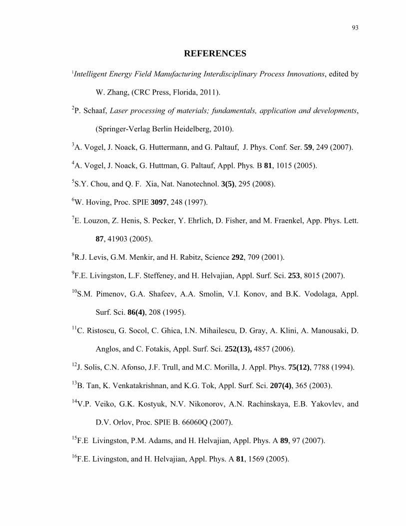
93
REFERENCES
1Intelligent Energy Field Manufacturing Interdisciplinary Process Innovations, edited by
W. Zhang, (CRC Press, Florida, 2011).
2P. Schaaf, Laser processing of materials; fundamentals, application and developments,
(Springer-Verlag Berlin Heidelberg, 2010).
3A. Vogel, J. Noack, G. Huttermann, and G. Paltauf, J. Phys. Conf. Ser. 59, 249 (2007).
4A. Vogel, J. Noack, G. Huttman, G. Paltauf, Appl. Phys. B 81, 1015 (2005).
5S.Y. Chou, and Q. F. Xia, Nat. Nanotechnol. 3(5), 295 (2008).
6W. Hoving, Proc. SPIE 3097, 248 (1997).
7E. Louzon, Z. Henis, S. Pecker, Y. Ehrlich, D. Fisher, and M. Fraenkel, App. Phys. Lett.
87, 41903 (2005).
8R.J. Levis, G.M. Menkir, and H. Rabitz, Science 292, 709 (2001).
9F.E. Livingston, L.F. Steffeney, and H. Helvajian, Appl. Surf. Sci. 253, 8015 (2007).
10S.M. Pimenov, G.A. Shafeev, A.A. Smolin, V.I. Konov, and B.K. Vodolaga, Appl.
Surf. Sci. 86(4), 208 (1995).
11C. Ristoscu, G. Socol, C. Ghica, I.N. Mihailescu, D. Gray, A. Klini, A. Manousaki, D.
Anglos, and C. Fotakis, Appl. Surf. Sci. 252(13), 4857 (2006).
12J. Solis, C.N. Afonso, J.F. Trull, and M.C. Morilla, J. Appl. Phys. 75(12), 7788 (1994).
13B. Tan, K. Venkatakrishnan, and K.G. Tok, Appl. Surf. Sci. 207(4), 365 (2003).
14V.P. Veiko, G.K. Kostyuk, N.V. Nikonorov, A.N. Rachinskaya, E.B. Yakovlev, and
D.V. Orlov, Proc. SPIE B. 66060Q (2007).
15F.E Livingston, P.M. Adams, and H. Helvajian, Appl. Phys. A 89, 97 (2007).
16F.E. Livingston, and H. Helvajian, Appl. Phys. A 81, 1569 (2005).
94
17F.E. Livingston, P. Adams, and H. Helvajian, Proc. SPIE 5662, 44 (2004).
18F.E. Livingston, P. Adams, and H. Helvajian, Appl. Surf. Sci. 247, 526 (2005).
19D.M. Bubb, J.S. Horwitz, J.H. Callahan, R.A. McGill, E.J. Houser, D.B. Chrisey, M.R.
Papantonakis, R.F. Haglund Jr, M.C. Galicia and A. Vertes, J. Vac. Sci. Technol.
A 19(5), 2698 (2001).
20D.M. Bubb, B. Toftmann, R.F. HaglundJr, J.S. Horwitz, M.R. Papantonakis, R.A.
McGill, P.W. Wu and D.B. Chrisey, Appl. Phys. A 74, 123 (2002).
21J. Mazumder and A. Kar, J. Metals. 9, 18 (1987).
22G. Sepold, and M. Grupp, Contents of the proceeding (LANE 2001), pp. 133.
23G. Horowitz, J. Mate. Res. 19, 1942 (2004).
24M. Katayama, Y.Tokuda, Y. Inoue, A. Usami and T. Wada, J. Appl. Phys. 69, 3541
(1991).
25Laser–Tissue Interaction IX, edited by S. L. Jacques, (SPIE Proc. Series Vol. 3254
Bellingham, WA, 1998).
26S.L. Jacques, Appl. Opt. 32, 2447 (1993).
27L.V. Zhigilei and B.J. Garrison, Appl. Phys. Lett. 74, 1341 (1999).
28A. Miotello and R. Kelly, Appl. Phys. A 69A, S67 (1999).
29R. Kelly and A. Miotello, Phys. Rev. E 60, 2616 (1999).
30M.M. Martynyuk, Sov. Phys. Tech. Phys. 21, 430 (1976).
31L.V. Zhigilei, P.B.S. Kodali, and B. J. Garrison, Chem. Phys. Lett. 276, 269 (1997).
32D. Bauerle, Laser Processing and Chemistry, (Springer Series in material science,
Berlin, Heidelberg: Springer-Verlag 1996).
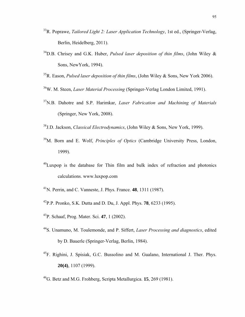
95
33R. Poprawe, Tailored Light 2: Laser Application Technology, 1st ed., (Springer-Verlag,
Berlin, Heidelberg, 2011).
34D.B. Chrisey and G.K. Huber, Pulsed laser deposition of thin films, (John Wiley &
Sons, NewYork, 1994).
35R. Eason, Pulsed laser deposition of thin films, (John Wiley & Sons, New York 2006).
36W. M. Steen, Laser Material Processing (Springer-Verlag London Limited, 1991).
37N.B. Dahotre and S.P. Harimkar, Laser Fabrication and Machining of Materials
(Springer, New York, 2008).
38J.D. Jackson, Classical Electrodynamics, (John Wiley & Sons, New York, 1999).
39M. Born and E. Wolf, Principles of Optics (Cambridge University Press, London,
1999).
40Luxpop is the database for Thin film and bulk index of refraction and photonics
calculations. www.luxpop.com
41N. Perrin, and C. Vanneste, J. Phys. France. 48, 1311 (1987).
42P.P. Pronko, S.K. Dutta and D. Du, J. Appl. Phys. 78, 6233 (1995).
43P. Schaaf, Prog. Mater. Sci. 47, 1 (2002).
44S. Unamuno, M. Toulemonde, and P. Siffert, Laser Processing and diagnostics, edited
by D. Bauerle (Springer-Verlag, Berlin, 1984).
45F. Righini, J. Spisiak, G.C. Bussolino and M. Gualano, International J. Ther. Phys.
20(4), 1107 (1999).
46G. Betz and M.G. Frohberg, Scripta Metallurgica. 15, 269 (1981).
96
47J.P. Moore, R.S. Graves and R.K. Williams, High Temp. High Pressures. 12, 579
(1980).
48R. Hultgren, et.al., Selected values of the thermodynamic properties of the elements,
(American Society for Metals, Metals Park, OH, 1973).
49H. Padamesee, J. Knobloch and T. Hays, RF superconductivity for Accelerators, 2nd
ed., (John Wiley & Sons, Inc., New York, 2008).
50J.A. Ramos, D.L. Bourell, and J.J. Beaman, Mat. Res. Soc. Symp. Proc. 758,
(Massachusetts, USA, 2002), pp. 53-61.
51W.M. Steen, and K.G. Watkins, J. Phys. IV. 3, 581 (1993).
52T.L. Perry, D. Werschmoeller, N.A. Duffie, X. Li, and F.E. Pfefferkorn, J. Manuf. Sci.
E-T ASME. 131, 031002 (2009).
53M. Vadali, C. Ma, N.A Duffie, S. Li and F.E. Pfefferkorn, Proc. International
Conference on MicroManufacturing, (ICOMM, Tokyo, Japan, 2011), pp. 331-
338.
54T.L. Perry, D. Werschmoeller, N.A. Duffie, X. Li, and F.E. Pfefferkorn, J. Manu. Sci.
E-T ASME 131, 021002 (2009).
55T.L. Perry, D. Werschmoeller, X. Li, F.E. Pfefferkorn, and N.A. Duffie, J. Manuf. Proc.
11, 74 (2009).
56P.F. Marella, D.B. Tuckerman, and R.F. Pease, Appl. Phys. Lett. 54, 1109 (1989).
57D.B. Tuckerman, and A. H. Weisberg, IEEE Electr. Device. Lett. 7, 1 (1986).
58T.M. Shao, M. Hua, H.Y. Tam and E.H.M. Cheung, Surf. Coat. Tech. 197, (2005).
59M. Bereznai, I. Pelsoczi, Z. Toth, K. Turzo, M. Radnai, Z. Bor, and A. Fazekas,
Biomaterials. 24, 4197 (2003).

97
60A. Temmler, K. Graichen, and J. Donath, J. Laser Technik. 7, 53 (2010).
61Y. G. Kim, J.K. Rye, D.J. Kim, H,J. Kim, S. Lee, B.H. Cha, H. Cha, and C.J. Kim, Jpn.
J. Appl. Phys. 43, 1315 (2004).
62S. Aldajah, O.O. Ajayi, G.R. Fenske, and S. Kumar, J. Tribol-T. ASME 125, 643
(2003).
63H. Tian, C. Xu, C.E. Reece, and M.J. Kelley, Appl. Surf. Sci. 257, 4781 (2011).
64F. Spaepen, Ultrafast Phenomena V: Proceedings of the Fifth OSA Meeting (New York:
Springer-Verlag, 1986), pp. 174-178.
65M. Senthilkumar, N.K. Sahoo, S. Thakur, and R.B. Tokas, Appl. Surf. Sci. 252, 1608
(2005).
66G. Gavrila, A. Dinescu, and D. Mardare, Roma. J. Info. Sci. Tech. 10, 291 (2007).
67B. Aune et.al., Phys. Rev. S T Accel. Beams 3, 092001 (2000).
68M. Pham Tu, K. Mbaye, L. Wartski, and J. Halbritter, J. Appl. Phys. 63, 4586 (1988).
69Z. Wang, A. Kawakami, Y. Uzawa, and B. Komiyawa, J. Appl. Phys. 79, 7837 (1996).
70J.C. Villegier et.al., Physica. C 326-327, 133 (1999).
71K. Mbaye, M. Pham Tu, N.T. Viet, L.Wartski and J.C. Villegier: Rev. Phys. Appl. 20,
457 (1985).
72R.P. Elliott, Constitution of Binary Alloys First Supplement, (McGraw-Hill, New York,
1965).
73P. Fabbricatore, P. Fernandes, G.C. Gualco, F. Merlo, R. Musenich, and R. Parodi, J.
Appl. Phys. 66(12), 5944 (1989).
74W. Lengauer, and P. Ettmayer, Monatsh. Chem. 117, 275 (1986).
98
75C. Angelkort et.al., Spectrachim. Acta. A 57, 2077 (2001).
76E. Carpene, P. Schaaf, M. Han, K.P. Lieb, and M. Shinn, Appl. Surf. Sci. 186, 195
(2002).
77Y.E.E-D Gamal, M. S.E-D Shafik and J. M. Daoud, J. Phys. D: Appl. Phys. 32, 423
(1999).
78H.U. Krebs, Int. J. of Non-Equilib. Pr. 10(3), 24 (1997).
79Bettis Jr. Appl. Opt. 31, 3448 (1992).
80Laser-induced plasma and applications, edited by L.J. Radziemski, D.A. Cremers (New
York, Marcel Dekker, Inc. 1992).
81P. Fabbricatore, P. Fernandes, G.C. Gualco, F. Merlo, R. Musenich, and R. Parodi, J.
Appl. Phys. 66, 5944 (1989).
82V.N. Zhitomirsky, I. Grimberg, L. Rapoport, N.A. Travitzky, R.L. Boxman,
S. Goldsmith, A. Raihel, I. Lapsker, and B.Z. Weiss, Thin Solid Films 326, 134
(1998).
83V.N. Zhitomirsky, I. Grimberg, L. Rapoport, N.A. Travitzky, R.L. Boxman, S.
Goldsmith, and B.Z. Weiss, Surf. Coat. Technol. 120, 219 (1999).
84A. Bendavid, P.J. Martin, T.J. Kinder, and E.W. Preston, Surf. Coat. Technol. 163, 347
(2003).
85K.L. Rutherford, P.W. Hatto, C. Davies, and I.M. Hutchings, Surf. Coat. Technol. 86,
472 (1996).
86M.S. Wong, W.D. Sproul, X. Chu, and S.A. Barnett, J. Vac. Sci. Technol. A 11(4), 528
(1993).

99
87M. Fenker, M. Balzer, R.V. Büchi, H.A. Jehn, H. Kappl, and J.J. Lee, Surf. Coat.
Technol. 163, 169 (2003).
88K.S. Havey, J.S. Zabinski, and S.D. Walck, Thin Solid Films 303, 238 (1997).
89M. Larsson, M. Bromark, P. Hedenqvist, and S. Hogmark, Surf. Coat. Technol. 91, 43
(1997).
90Z. Han, X. Hu, J. Tian, G. Li, and G. Mingyuan, Surf. Coat. Technol. 179, 188 (2004).
91M. Benkahoul, E. Martinez, A. Karimi, R. Sanjines, and F. Levy, Surf. Coat. Technol.
180, 178 (2004).
92C.S. Sandu, M. Benkahoul, M. Parlinska-Wojtan, R. Sanjines, and F. Levy, Surf. Coat.
Technol. 200, 6544 (2006).
93N. Hayashi, I.H. Murzin, I. Sakamoto, and M. Ohkubo, Thin Solid Films. 259, 146
(1995).
94M.L. Klingenberg, and J.D. Demaree, Surf. Coat. Technol. 146, 243 (2001).
95K. Baba, R. Hatada, K. Udoh, and K. Yasuda, Nucl. Instrum. Methods Phys. Res. B
Beam Interact. Mater. Atoms 127, 841 (1997).
96X.T. Zeng, Surf. Coat. Technol. 11, 75 (1999).
97G. Cappuccio, U. Gambardella, A. Morone, S. Orlando, and G.P. Parisi, Appl. Surf.
Sci. 109, 399 (1997).
98R.E. Teece, J.S.Horwitz, J.H. Classssen, and D.B.Chrisey, Appl. Phys. Lett. 65, 22
(1994).
99A. Bhat, X. Meng, A. Wong and T.V. Duzer, Supercond. Sci. Tech. 10(3), 1032 (1999).
100K.S. Keskar, T. Yamashita, and Y. Onodera, Jpn. J. Appl. Phys. 10(3), 370 (1971).
101H. Knau, A. Welti, A. Mielke, S. Senz and H.E. Stier, Physica C 182, 1 (1991).
100
102S. Isagawa, Appl. Phys. 52, 921 (1981).
103P. Fabbricatore, P. Frenandes, G.C. Gulaco, R. Masenich and R. Parodi, IEEE T.
Magn. 25, 1865 (1988).
104V.M. Pan, V.P. Gorishnyak, E.M. Rudenko, V.E. Shaternik, M.V. Belous,
S.A. Koziychuk and F.I. Korzhinsky, Cryogenics 23(5), 258 (1983).
105Kenji Kawaguchi and Mitsugushohma, Jpn. J. Appl. Phys. 30, 2088 (1991).
106R.E. Teece, J.S. Horwitz, D.B. Chrisey, E.P. Donovan and S.B. Quadri, Chem. Mater.
6, 2205 (1994).
107V. Boffa, V. Gambardella, V. Marotta, A. Morone, F. Murtas, S. Orlando, and
G.P. Parisi, App. Surf. Sci. 106, 361 (1996).
108K. Mittag, Cryogenics 13(2), 94 (1973).
109H. Knau, A. Welti, A. Mielke, S. Senz and H.E. Stier, Physica. C 182, 39 (1991).
110A.J. Heeger, Rev. Mod. Phys. 73, 681 (2001).
111A. P. Ghosh, L.J. Gerenser, C.M. Jarman, and J.E. Fornalik, Appl. Phys. Lett. 86(22),
223503 (2005).
112F. Bundgaard, T. Nielsen, D. Nilsson, P. Shi, G. Perozziello, A. Kristensen, and
O. Geschke, Proceedings of the mTAS, (Malmo, Sweden, 2004) pp. 372– 374.
113G. Khanarian, Opt. Eng. 40, 1024 (2001).
114R. Scheller, ETP 99 World Congress, (1999).
115T. Scrivani, R. Benavente E. Perez, and J.M. Perena, Macromol. Chem. Phys. 202,
2547 (2001).
116D.M. Bubb and R.F. Haglund, “Resonant Infrared Pulsed Laser Ablation and
Deposition of Thin Polymer Films, in Pulsed Laser Deposition of Thin Films:
101
Applications-Led Growth of Functional Materials,” edited by R. Eason (John
Wiley and Sons, Inc., New York, 2006).
117D.M. Bubb, J.S. Horwitz, J.H. Callahan, R.A. McGill, E.J. Houser, D.B. Chrisey,
M.R. Papantonakis, R.F. Haglund, M.C. Galicia, and A. Vertes, J. Vac. Sci. Tech.
A 19(5), 2698 (2001).
118M.R. Papantonakis and R.F. Haglund, Appl Phys A-Mater. 79(7), 1687 (2004).
119N.L. Dygert, A. P. Gies, K.E. Schriver, and R.F. Haglund, Appl. Phys. A-Mater. 89(2),
481 (2007).
120M.R. Papantonakis, E. Herz, D.L. Simonsen, U.B. Wiesner, and R.F. Haglund, Jr.,
“Deposition of functionalized nanoparticles in multilayer thin-film structures by
resonant infrared laser radiation, in Laser-based Micro- and Nanopackaging and
Assembly,” edited by. W. Pfleging, Y. Lu, K. Washio, F. G. Bachmann and W.
Hoving, (Proceedings of SPIE, 6459, 64590X, 2007).
121H. Injeyan and G. Goodno, High Power Laser Handbook, (McGraw-Hill Companies,
Inc., China, 2010).
122C. Liu, J. Yu, X. Sun, J. Zhang and J. He, Poly. Degrad. Stab. 81, 197 (2003).
123S.M. Avanesyan, A. Halabica, S.L. Johnson, M.J. Kelley, J.M. Klopf, H.K. Park,
K.E. Schriver, S. Singaravelu and R.F. Haglund, Jr., Proc. SPIE 7585, 758507
(2010).
124S.L. Johnson, “Resonant-infrared laser ablation of polymers: Mechanisms and
applications,” Ph.D. thesis, (Vanderbilt University, 2008).
125S.L. Johnson, D.M. Bubb and R.F. Haglund Jr., Appl. Phys. A 96, 627 (2009).

102
126D.V. Rosato, N.R. Schott, and M.G. Rosato, Plastics Engineering, Manufacturing &
Data Handbook, (Springer, Berlin, 2001).
103
Appendix A
EXPERIMENTAL SETUP
I. PLD 5000
A. Pumping Stack
A PVD Products Inc., PLD 5000 system (Technical details courtesy of PVD Products
Inc.) shown schematically in Fig. A1, was used for all the experiments performed at
Jefferson Lab. Installing and commissioning it were key tasks. The system consists of a
vacuum chamber made up of stainless steel, attached to a water cooled Pfeiffer vacuum
turbo drag pump and splinter screen. The turbo pump provides a pumping speed of 1,200
l/sec. A Leybold D-25B rotary vane mechanical pump prepared for oxygen gas (Fomblin
oil) is provided to evacuate the chamber and back the turbo pump. This package provided
a base pressure below 5 × 10⁻⁷ Torr. When gas is passed through, the chamber can sustain
the maximum positive pressure of 625 Torr.
A mechanical pump is used to evacuate the chamber and/or loadlock (optional)
during the roughing cycle of pump down and also backs the turbo pump during operation.
The foreline valve and the rough valve isolate the mechanical pump. The foreline valve
connects the mechanical pump to the turbo pump, and once the foreline valve is open the
turbo pump will evacuate. The rough valve connects the mechanical pump to the
chamber, and once the rough valve is open the chamber will evacuate.
To spin up the turbo pump:
• Close the chamber gate valve (software interface)
104
• Switch on the mechanical pump (software interface)
• Open the foreline valve (software interface)
• Switch on the turbo pump (software interface)
• Wait for the turbo pump to reach full speed (625 rpm)
To spin down and turn off the turbo pump:
• Close the chamber gate valve (software interface)
• Switch off the turbo pump (software interface)
• Wait for the turbo pump to reach half of the maximum rotation speed
• Close the foreline valve (software interface)
• Switch off the mechanical pump (software interface, if not longer needed)
B. Loadlock
An optional loadlock with transfer arm is mounted to the system. The loadlock has a
quick access door for sample loading. The sample is transferred into the main chamber
with a magnetically coupled linear actuator. The loadlock includes a mechanical pump,
roughing valve, foreline valve, vent valve, pressure relief valve, convectron gauge, and
ion gauge.
C. Substrate Assembly
An optional substrate rotation assembly sits on top of a 2.75” Z-stage. The Z-stage
movement is controlled by a stepper motor and has mechanical hard stops to limit the
range of motion. The Z-stage can be lowered for substrate loading/unloading and raised
for deposition. The rotary motion feedthrough is magnetically coupled and the entire
assembly moves in unison with the motion of the Z-stage.
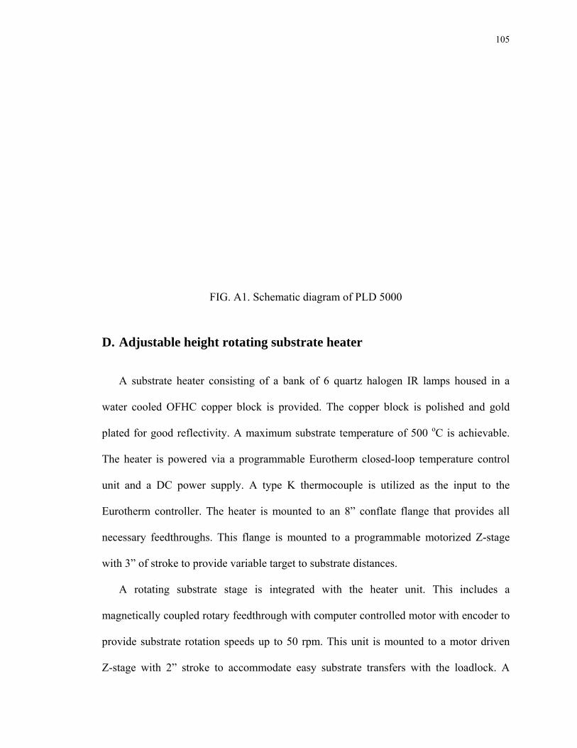
105
FIG. A1. Schematic diagram of PLD 5000
D. Adjustable height rotating substrate heater
A substrate heater consisting of a bank of 6 quartz halogen IR lamps housed in a
water cooled OFHC copper block is provided. The copper block is polished and gold
plated for good reflectivity. A maximum substrate temperature of 500 oC is achievable.
The heater is powered via a programmable Eurotherm closed-loop temperature control
unit and a DC power supply. A type K thermocouple is utilized as the input to the
Eurotherm controller. The heater is mounted to an 8” conflate flange that provides all
necessary feedthroughs. This flange is mounted to a programmable motorized Z-stage
with 3” of stroke to provide variable target to substrate distances.
A rotating substrate stage is integrated with the heater unit. This includes a
magnetically coupled rotary feedthrough with computer controlled motor with encoder to
provide substrate rotation speeds up to 50 rpm. This unit is mounted to a motor driven
Z-stage with 2” stroke to accommodate easy substrate transfers with the loadlock. A

106
stainless steel substrate spinner assembly and shaft connected to the rotary feedthrough is
provided.
E. Liquid nitrogen cooled target manipulator
The target manipulator includes a large cylindrical electrode nickel plated OHFC
copper liquid nitrogen reservoir that houses six stainless steel target pedestals. Three
pedestals are for frozen liquid (MAPLE) targets, and three pedestals are used for solid
targets. The MAPLE target pedestals are in excellent thermal contact with the reservoir
via copper brushes. Each of the pedestals is held in place via a set of high quality ball
bearings located within the reservoir housing. The shaft of each of the pedestals includes
a spur gear. Upon indexing to the proper position, this spur meshes with a second spur
gear driven by an appropriate motor drive with sufficient torque to rotate the one active
target pedestal. Rotation speed up to 12 rpm is provided. All target indexing and target
rotation functions are computer controlled.
The liquid nitrogen reservoir is bottom fed via a stainless steel tube and includes a
similar vent line. A type K thermocouple is connected to the reservoir and a temperature
readout display is provided. Infrared heat lamps sit beside the LN2 reservoir and can be
used to quickly heat the reservoir when the chamber is to be vented.
A molybdenum plate sits directly above the target assembly to minimize cross
contamination between targets and to help thermally isolate the targets from the substrate
heater. This plate includes a slot to expose the active ablation target to the incident laser
beam and holes that line up under the fill tubes.
107
F. Intelligent Window
The intelligent window keeps the optical beam path clean and allows the laser beam
energy to be monitored inside the deposition chamber. The unit includes an
electropnuumatic linear-motion feedthrough with a reflector that diverts the laser beam to
a Coherent PM 150 air cooled thermopile sensor with an EPM-1000 readout electronic
unit.
A motorized drive is provided to rotate an internal sacrificial CaF disc 6” in diameter
to expose new window surface to keep the beam path clean for extended periods. The
laser beam entrance window to deposition chamber is a 2” CaF window sealed via a pair
of differentially pumped Viton 0-rings.
G. Optical Train
A complete set of CaF optics is provided to cover the range from 1 to 8 μm to be
compatible with the FEL. One of the beam tuning mirrors is held in a programmable
kinematic mirror mount with programmable actuator that allows the focused laser beam
to be rastered over the active target diameter. This rastering mirror moves the laser beam
on the target; which raster’s ~1.8 inches on the target. The focus lens is mounted in a
motor driven linear translation stage that keeps the beam spot size constant during the
rastering process. The laser beam is incident at an angle of 60o to normal to the rotating
target, which is 2” in diameter. The raster mirror and translation stages are both
controlled via computer. The complete assembly is housed within a laser safe enclosure
with large access door.
108
H. Computer Control Software Package
The system is run via laptop computer with a LabVIEW interface and an Opto22 PLC
control system. The computer provides both manual step-by-step operation of all valves
on the system as well as auto pump/vent features for the main chamber and loadlock. The
computer controls the laser beam raster pattern, substrate temperature profiles, target and
substrate rotation speeds, substrate height, MFC flow rates, process pressure in the
deposition chamber, target indexing, and full control over the Intelligent Window.
II. LASER SYSTEMS
A brief introduction to the pulsed lasers used is presented here.
A. High Intensity Peak Power Oscillator (HIPPO)
The Spectra-Physics High Intensity Peak Power Oscillator (HIPPO) comprises a
solid-state laser head and a Model J80, dual-diode, pump power supply. The Nd:YVO4
(Vanadate) based laser head is optimized for high peak power and high average power,
with superior pulse stability. Vanadate is a popular solid state laser host due to its high
gain and because it can provide high power laser emission at high pulse repetition rates.
Being a solid state active media, Vanadate exhibits thermal lensing caused by the
temperature gradients inside the crystalline material. Temperature gradient creates an
optical index gradient that acts as a lens. The effective focal length of this thermal lens is
determined in part by the amount of heat deposited in the crystal from the pump energy.
The more pump energy applied to the crystal, the stronger the thermal lens and the
shorter the effective focal length. The laser head (fundamental) provides 1064 nm output

109
alone and can include an optional second harmonic generator (532 nm), third harmonic
generator (355 nm) or fourth harmonic generator (266 nm).
The HIPPO uses a W-fold cavity for convenient end-pumping the Nd:YVO4
(Vanadate) lasing media crystal. A high reflector and output coupler define the cavity
length. The latter allows a portion of the cavity light to pass out of the laser. To generate
high energy pulses, two high-powered, acousto-optic Q-switches are placed in the cavity
to act as switches to turn the laser on and off from 15 Hz to 300 kHz. Two high-power,
thermally-stabilized, Spectra Physics FC bar laser diodes in the Model J80 power supply
provide 2x26 W of 808 nm pump power to the laser cavity via fiber-optic cables. These
cables attach to the laser head by connectors that maintain the alignment of the output
from the fiber to the components inside the laser head.
A telescopic setup inside each input focuses the pump light through a dichroic mirror
and into the end of the Vanadate crystal. The dichroic mirrors are highly transmissive at
the diode pump wavelength and highly reflective at 1064 nm. The pump beams are
absorbed by the crystal and 1064 nm and infrared (IR) intracavity light is generated.
To provide a source for output power monitoring, the output is sampled using a beam
splitter and photodiode that are placed between the output coupler and the end of the
laser. To provide safety, a mechanical shutter is placed inside the housing to stop the
1064 nm lasing action in its default closed position. It can be commanded to open and
close via remote command but is closed when power is not applied to the system and will
not open until commanded to do so.
110
B. Free Electron Laser (FEL)
The output of a Free-Electron Laser (FEL) is generated by stimulated emission of
radiation. Its emission properties are essentially the same as any other laser – partial
coherence, mono-chromaticity, etc., but the method used to generate the laser output in a
FEL is much different than in a conventional laser. A FEL feeds a beam of electrons from
a particle accelerator through a line of alternating magnets called an undulator or wiggler.
The magnetic field causes the electrons to wiggle when they travel through the undulator
and the electrons will emit radiation as their velocity changes. Most particle accelerators
deliver a train of electron pulses. The interaction of the electrons with the combined
magnetic and radiation field results in a periodic force on the electrons. As a result a
velocity spread is induced on the electrons in the electron beam. After the electrons have
propagated a certain distance, this velocity modulation is translated into a density
modulation on the electron beam, i.e., bunches are formed approximately a radiation
wavelength apart. Therefore the electron beam is capable of amplifying a radiation field
coherently. Mirrors are used to reflect the radiation back and forth through the undulator.
The electrons are not bound to any atoms, hence the term Free-Electron Laser. The
cavity length is chosen such that the optical pulse overlaps with a fresh electron pulse
after one round trip at the entrance of the undulator. The efficiency of the FEL depends
on the wavelength generated and can vary from tens of percent at mm wavelengths to a
fraction of a percent in the UV. However since the energy stored in the electron beam
increases as the wavelength decrease, high peak powers can be produced at all
wavelengths. The efficiency of a FEL can be enhanced in two ways; first a non-uniform
undulator can be used to increase the extraction efficiency. Second the energy stored in
111
the electron beam after the interaction can be recovered, thereby increasing the overall
efficiency of the system. Therefore the FEL can be tuned in principle over a very large
wavelength range from m to nm. The output wavelength of the FEL is related to the
wiggler periodically spacing, λwiggler, by the following equation
2 1 , 12
where γ is the electron beam energy in terms of its rest mass, and κ is a term that is
dependent on the magnitude and orientation of the magnetic field, B. However this range
is limited in practice by the type of particle accelerator used (which fixes the energy
range covered) and the fact that undulators have a fixed period and the strength of the
magnetic field can be varied only within certain limits. Nevertheless the tuning range
which can be obtained with FEL is in general much larger than those obtained with
conventional lasers. Typical electron beam energies are tens of MeV and an undulator
period of several centimeters. Oscillator FELs have also been operated in the UV, visible
and radar wavelength regime. In general the undulator period must be reduced and the
electron beam energy increased to obtain shorter wavelengths. The wavelength tunability,
high efficiency and reliability can make the FEL very attractive for industrial
applications.
i. Meter calibration for FEL experiments
To find the energy per pulse of the FEL hitting on the organic target kept inside the
chamber, two energy meters were used. Fig. A2 shows the schematic diagram and actual
image of the two meters used, one kept inside the chamber and the other outside the
chamber. Such that, while doing actual experiment, meter 2 is removed and values from

112
meter 1 is taken into consideration to determine the energy per pulse of the FEL
irradiated on the target. Bunches of individual long and short pulses were sent and the
readings were noted from both the meters simultaneously. The linear fit of these values
were plotted as shown in Fig. A3. Using the linear equation obtained, the energy of each
pulse can be found.
FIG. A2. Schematic and actual picture of positioning the meter used for calibration.
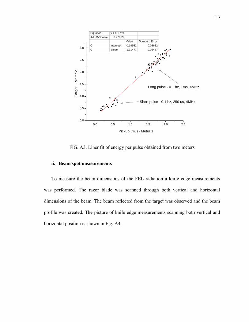
113
0.0 0.5 1.0 1.5 2.0 2.50.0
0.5
1.0
1.5
2.0
2.5
3.0
Short pulse - 0.1 hz, 250 us, 4MHz
Pickup (mJ) - Meter 1
Targ
et -
Met
er 2
Equation y = a + b*xAdj. R-Square 0.97863
Value Standard ErrorC Intercept 0.14952 0.03682C Slope 1.31477 0.02467
Long pulse - 0.1 hz, 1ms, 4MHz
FIG. A3. Liner fit of energy per pulse obtained from two meters
ii. Beam spot measurements
To measure the beam dimensions of the FEL radiation a knife edge measurements
was performed. The razor blade was scanned through both vertical and horizontal
dimensions of the beam. The beam reflected from the target was observed and the beam
profile was created. The picture of knife edge measurements scanning both vertical and
horizontal position is shown in Fig. A4.
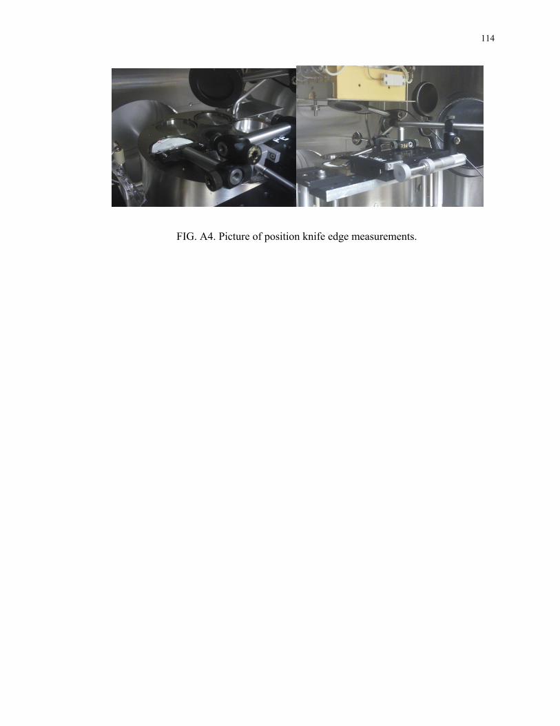
114
FIG. A4. Picture of position knife edge measurements.
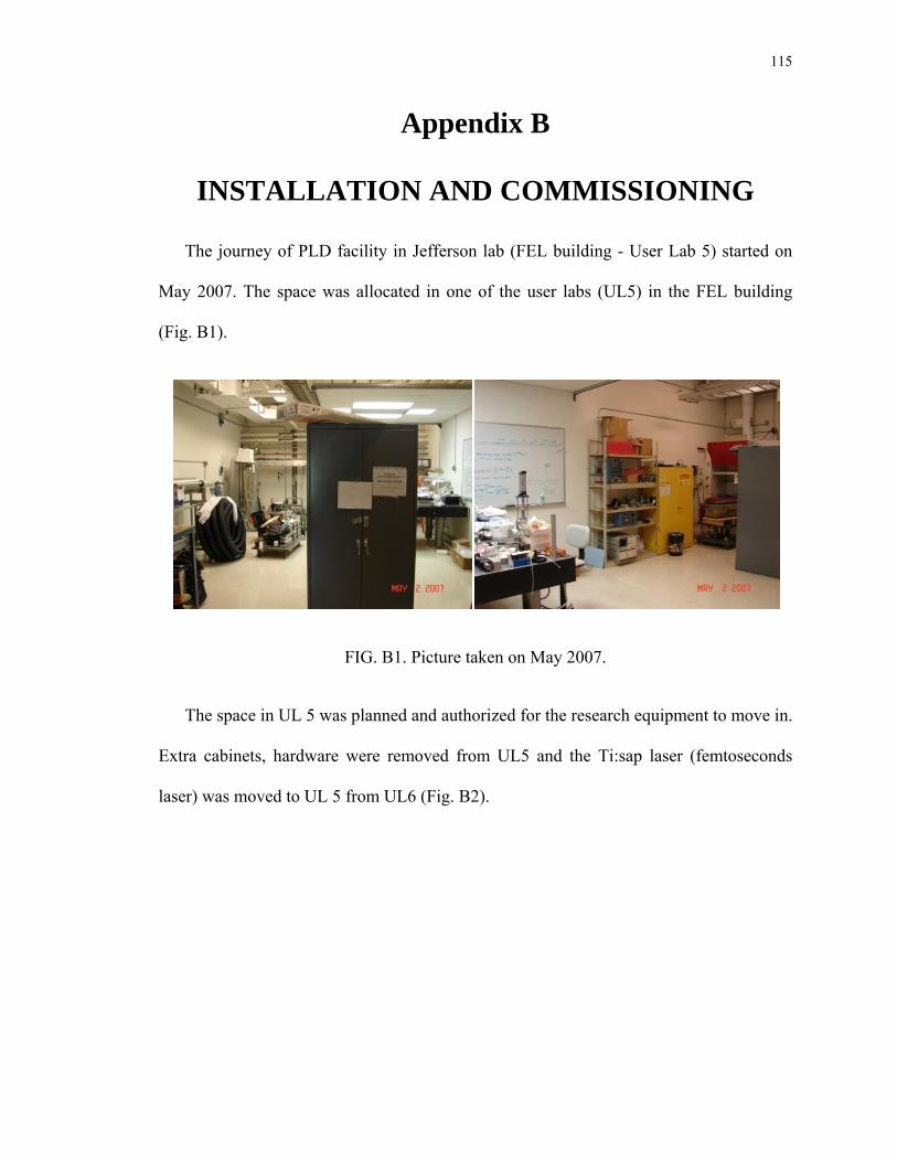
115
Appendix B
INSTALLATION AND COMMISSIONING
The journey of PLD facility in Jefferson lab (FEL building - User Lab 5) started on
May 2007. The space was allocated in one of the user labs (UL5) in the FEL building
(Fig. B1).
FIG. B1. Picture taken on May 2007.
The space in UL 5 was planned and authorized for the research equipment to move in.
Extra cabinets, hardware were removed from UL5 and the Ti:sap laser (femtoseconds
laser) was moved to UL 5 from UL6 (Fig. B2).
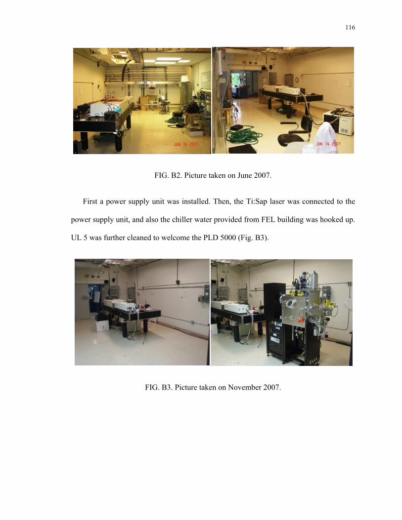
116
FIG. B2. Picture taken on June 2007.
First a power supply unit was installed. Then, the Ti:Sap laser was connected to the
power supply unit, and also the chiller water provided from FEL building was hooked up.
UL 5 was further cleaned to welcome the PLD 5000 (Fig. B3).
FIG. B3. Picture taken on November 2007.
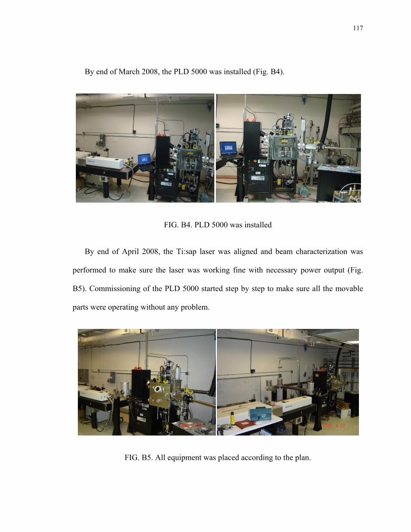
117
By end of March 2008, the PLD 5000 was installed (Fig. B4).
FIG. B4. PLD 5000 was installed
By end of April 2008, the Ti:sap laser was aligned and beam characterization was
performed to make sure the laser was working fine with necessary power output (Fig.
B5). Commissioning of the PLD 5000 started step by step to make sure all the movable
parts were operating without any problem.
FIG. B5. All equipment was placed according to the plan.
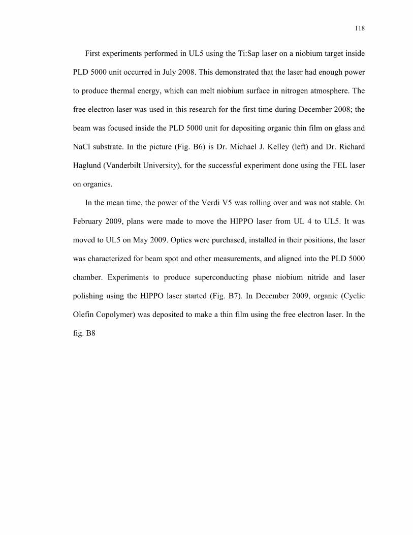
118
First experiments performed in UL5 using the Ti:Sap laser on a niobium target inside
PLD 5000 unit occurred in July 2008. This demonstrated that the laser had enough power
to produce thermal energy, which can melt niobium surface in nitrogen atmosphere. The
free electron laser was used in this research for the first time during December 2008; the
beam was focused inside the PLD 5000 unit for depositing organic thin film on glass and
NaCl substrate. In the picture (Fig. B6) is Dr. Michael J. Kelley (left) and Dr. Richard
Haglund (Vanderbilt University), for the successful experiment done using the FEL laser
on organics.
In the mean time, the power of the Verdi V5 was rolling over and was not stable. On
February 2009, plans were made to move the HIPPO laser from UL 4 to UL5. It was
moved to UL5 on May 2009. Optics were purchased, installed in their positions, the laser
was characterized for beam spot and other measurements, and aligned into the PLD 5000
chamber. Experiments to produce superconducting phase niobium nitride and laser
polishing using the HIPPO laser started (Fig. B7). In December 2009, organic (Cyclic
Olefin Copolymer) was deposited to make a thin film using the free electron laser. In the
fig. B8
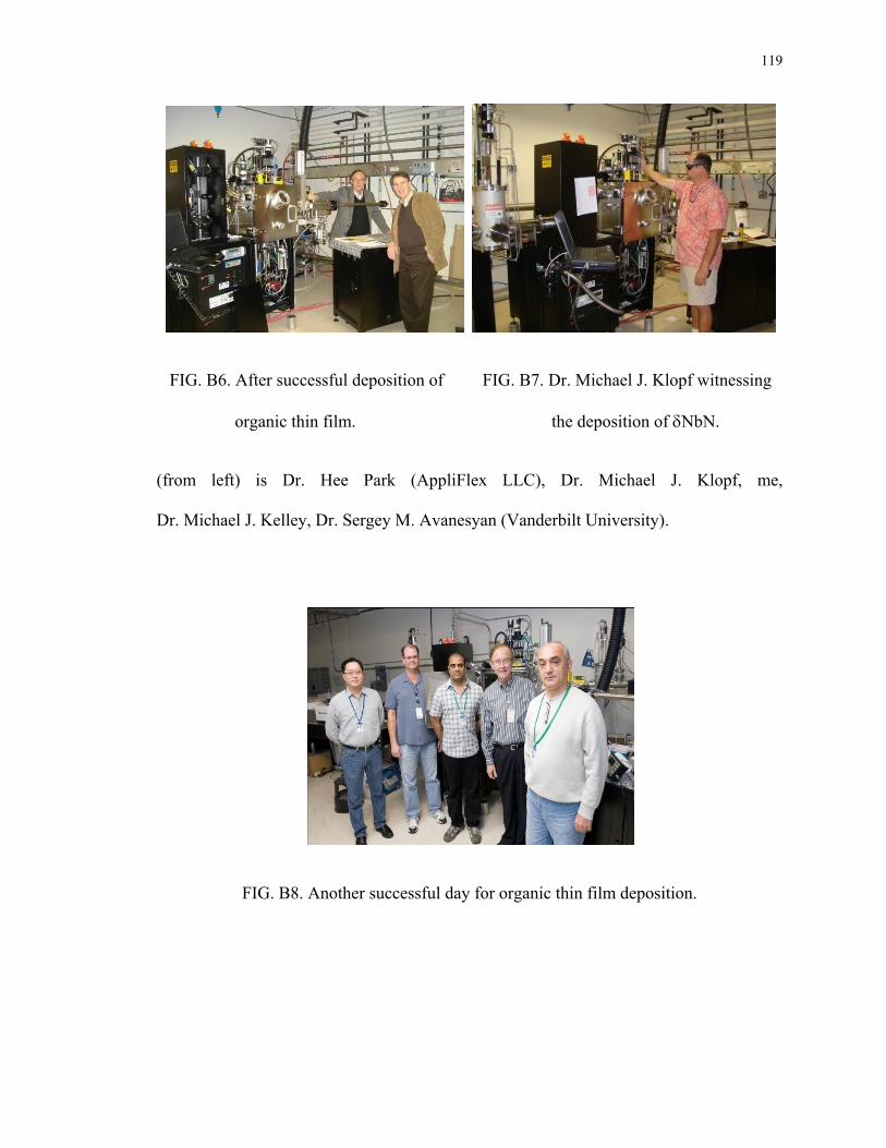
119
FIG. B6. After successful deposition of FIG. B7. Dr. Michael J. Klopf witnessing
organic thin film. the deposition of δNbN.
(from left) is Dr. Hee Park (AppliFlex LLC), Dr. Michael J. Klopf, me,
Dr. Michael J. Kelley, Dr. Sergey M. Avanesyan (Vanderbilt University).
FIG. B8. Another successful day for organic thin film deposition.
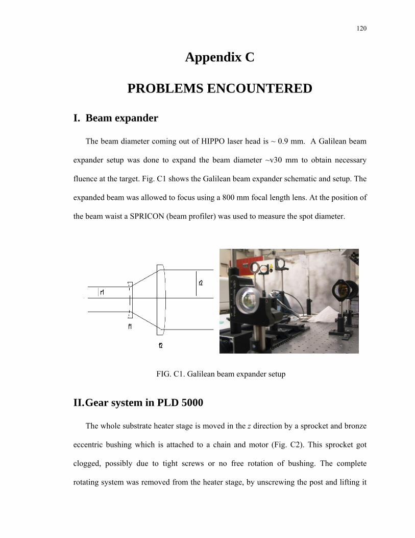
120
Appendix C
PROBLEMS ENCOUNTERED
I. Beam expander
The beam diameter coming out of HIPPO laser head is ~ 0.9 mm. A Galilean beam
expander setup was done to expand the beam diameter ~v30 mm to obtain necessary
fluence at the target. Fig. C1 shows the Galilean beam expander schematic and setup. The
expanded beam was allowed to focus using a 800 mm focal length lens. At the position of
the beam waist a SPRICON (beam profiler) was used to measure the spot diameter.
FIG. C1. Galilean beam expander setup
II. Gear system in PLD 5000
The whole substrate heater stage is moved in the z direction by a sprocket and bronze
eccentric bushing which is attached to a chain and motor (Fig. C2). This sprocket got
clogged, possibly due to tight screws or no free rotation of bushing. The complete
rotating system was removed from the heater stage, by unscrewing the post and lifting it
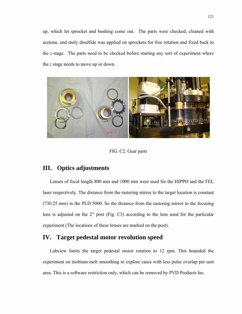
121
up, which let sprocket and bushing come out. The parts were checked, cleaned with
acetone, and moly disulfide was applied on sprockets for free rotation and fixed back to
the z-stage. The parts need to be checked before starting any sort of experiment where
the z stage needs to move up or down.
FIG. C2. Gear parts
III. Optics adjustments
Lenses of focal length 800 mm and 1000 mm were used for the HIPPO and the FEL
laser respectively. The distance from the rastering mirror to the target location is constant
(730.25 mm) in the PLD 5000. So the distance from the rastering mirror to the focusing
lens is adjusted on the 2” post (Fig. C3) according to the lens used for the particular
experiment (The locations of these lenses are marked on the post).
IV. Target pedestal motor revolution speed
Labview limits the target pedestal motor rotation to 12 rpm. This bounded the
experiment on niobium melt smoothing to explore cases with less pulse overlap per unit
area. This is a software restriction only, which can be removed by PVD Products Inc.

122
FIG. C3. Optics height adjustment according to the experiment.
V. Substrate shutter
Before starting the deposition on any substrate the surface of the target should be
clean. The substrate shutter should be closed for few minutes, while the laser is rastering
the surface. After few minutes we need to open the substrate shutter. Sometimes the
shutter does not move to the open position completely (Fig. C4), which can cause two
problems. First, the deposition is not uniform on the substrate because the shutter is half
way in between the substrate and the target. Second, to change the target-substrate throw
distance we need to move the substrate holder down from the z-stage. As the shutter is
half way blocking the substrate position, the substrate holder hits the substrate shutter and
if not noticed, then the rod of the substrate holder bends.
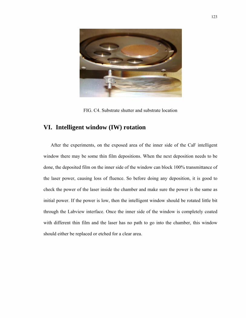
123
FIG. C4. Substrate shutter and substrate location
VI. Intelligent window (IW) rotation
After the experiments, on the exposed area of the inner side of the CaF intelligent
window there may be some thin film depositions. When the next deposition needs to be
done, the deposited film on the inner side of the window can block 100% transmittance of
the laser power, causing loss of fluence. So before doing any deposition, it is good to
check the power of the laser inside the chamber and make sure the power is the same as
initial power. If the power is low, then the intelligent window should be rotated little bit
through the Labview interface. Once the inner side of the window is completely coated
with different thin film and the laser has no path to go into the chamber, this window
should either be replaced or etched for a clear area.

124
FIG. C5. Position of Intelligent window
VII. Aperture near the intelligent window was removed
The aperture outside the PLD chamber was ~10 mm. The beam diameter of the FEL
was bigger than this aperture, which was clipping the beam entering inside the chamber.
So the aperture was removed.
VIII. Chiller water facility
The PLD 5000 unit is connected to the chiller water provided by the FEL facility.
Chiller water is transported through stainless steel pipes. Inside the lab, the water is
transferred through copper pipe, which could have some dust/rust particles. These
particles got clogged inside the PLD unit and the heat produced due to the turbo and other
motors were not removed from the machine causing an explosion of the return supply
water pipe, above the PLD 5000 unit. Thus a filter is attached (Fig. C6) to filter these dust
particles and provide chilled water inside the unit preventing further explosions.
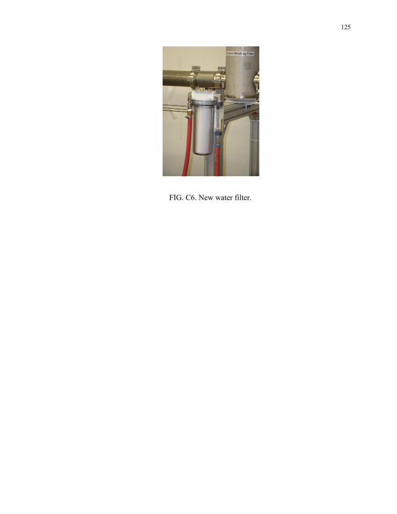
125
FIG. C6. New water filter.
126
VITA
Senthilraja Singaravelu (Raja) Department of Physics, ODU 4600 Elkhorn Avenue, Norfolk, VA 23529.
EDUCATION: • Ph.D, Physics, Old Dominion University, Norfolk, VA. [May 2012] • M.S., Physics, Old Dominion University, Norfolk, VA [May 2006] • M.Sc., Physics (Specialization in Electronics), Bharathiar University, India [April 2001] • B.Sc., Physics, University of Madras, India [March 1998]
PATENT: • Patent disclosure submitted: “Enhanced Superconducting Surface for Nb SRF Cavities
Obtained by Gas Laser Nitriding,” Thomas Jefferson National Laboratory, Newport News, VA.
HONORS AND AWARDS: • Article “Laser Nitriding of Niobium for application to Superconducting Radio-Frequency
Accelerator Cavities” was selected for Virtual Journal of Applications of Superconductivity, November 15, 2011, published by AIP and APS.
• Honorable Mention for the Visiting Scholar Award (Second prize) for the paper presented at 9th and 10th Annual Graduate Research Symposium, March 2010 & 2011 respy., The College of William & Mary, USA.
• Third prize for the poster presentation presented at Jefferson Lab Annual Users meeting, June 2010, Thomas Jefferson laboratory, USA.
• Second prize for the poster presentation presented at Tidewater Virginia Chapter & Washington, D.C area Chapter of Sigma Xi-11th Annual Student Research Poster Session, November 2009, Christopher Newport University, USA.
• Best post graduate thesis award for the topic entitled “Vacuum evaporated vanadium pentoxide (V2O5) thin films,” Bharathiar University, India.
• First in the class, B.Sc. (Physics), July 1995 – March 1998, University of Madras, India. PUBLICATIONS:
• S. Singaravelu, J.M. Klopf, G. Krafft, M.J. Kelley, “Laser Nitriding of Niobium for application to Superconducting Radio-Frequency Accelerator Cavities,” J. Vac. Sci. Tech. B, 29, 061803, (2011).
• S. Singaravelu, J.M. Klopf, C. Xu, G. Krafft, M.J. Kelley, “Laser Polishing of Niobium for application to Superconducting Radio-Frequency Cavities,” – Submitted to J. Vac. Sci. Tech. B, 2011.
• S. Singaravelu, J.M. Klopf, K. E. Schriver, H.K. Park, M.J. Kelley, R.F. Haglund Jr., “Resonant Infrared Pulsed Laser Deposition of Cyclic Olefin Copolymer Films”, - Submitted to App. Phys. A, 2011.
• S. M. Avanesyan, A. Halabica, S. L. Johnson, M. J. Kelley, J. M. Klopf, H. K. Park, K. E. Schriver, S. Singaravelu, R. F. Haglund, Jr., “Deposition of polymer barrier materials by resonant infrared pulsed laser ablation,” Proc. SPIE, vol. 7585, 2010.


![3D Printing of Thermoresponsive Polyisocyanide (PIC ...noviosense.com/wp-content/uploads/2018/11/polymers... · Polymers 2018, 10, 555 2 of 11 polymers [6,7], metals and alloys [8,9],](https://img.dokumen.tips/doc/110x75/5f035ab57e708231d408ccd9/3d-printing-of-thermoresponsive-polyisocyanide-pic-polymers-2018-10-555-2.jpg)