Embed Size (px)
Citation preview
REV. 0
Information furnished by Analog Devices is believed to be accurate andreliable. However, no responsibility is assumed by Analog Devices for itsuse, nor for any infringements of patents or other rights of third partieswhich may result from its use. No license is granted by implication orotherwise under any patent or patent rights of Analog Devices.
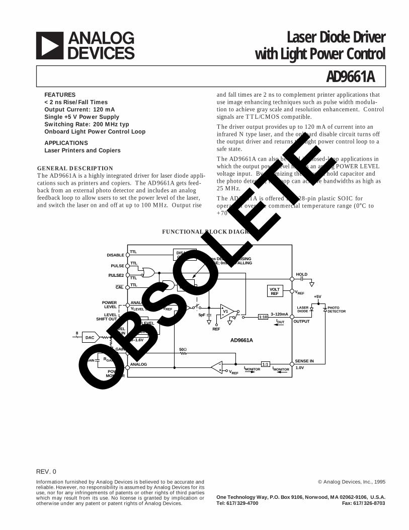
a Laser Diode Driverwith Light Power Control
AD9661A
© Analog Devices, Inc., 1995
One Technology Way, P.O. Box 9106, Norwood, MA 02062-9106, U.S.A.
Tel: 617/329-4700 Fax: 617/326-8703
FEATURES
< 2 ns Rise/Fall Times
Output Current: 120 mA
Single +5 V Power Supply
Switching Rate: 200 MHz typ
Onboard Light Power Control Loop
APPLICATIONS
Laser Printers and Copiers
and fall times are 2 ns to complement printer applications thatuse image enhancing techniques such as pulse width modula-tion to achieve gray scale and resolution enhancement. Controlsignals are TTL/CMOS compatible.
The driver output provides up to 120 mA of current into aninfrared N type laser, and the onboard disable circuit turns offthe output driver and returns the light power control loop to asafe state.
The AD9661A can also be used in closed-loop applications inwhich the output power level follows an analog POWER LEVELvoltage input. By optimizing the external hold capacitor andthe photo detector, the loop can achieve bandwidths as high as25 MHz.
The AD9661A is offered in a 28-pin plastic SOIC foroperation over the commercial temperature range (0°C to+70°C).
GENERAL DESCRIPTIONThe AD9661A is a highly integrated driver for laser diode appli-cations such as printers and copiers. The AD9661A gets feed-back from an external photo detector and includes an analogfeedback loop to allow users to set the power level of the laser,and switch the laser on and off at up to 100 MHz. Output rise
FUNCTIONAL BLOCK DIAGRAM
PULSE2
DISABLECIRCUIT
DELAY
TTL
TTL
TTL
TTL
DISABLE
PULSE
DAC
CGAIN
ANALOGPOWERLEVEL
LEVELSHIFT OUT
LEVELSHIFT IN
50Ω
REF
5pF
*
*13ns DELAY ON RISINGEDGE; 0ns ON FALLING
1:103–120mA
IOUT
VOLTREF
1:1
HOLD
VREF
LASERDIODE
+5V
PHOTODETECTOR
VREF
IMONITORANALOG
POWERMONITOR
RGAIN
GAIN
0–1.6V
CAL
VLEVEL SHIFT IN + VREF
SENSE IN
1.0V
8
IMONITOR
V1
OUTPUTLEVELSHIFT
CIRCUIT
AD9661A
OBSOLETE
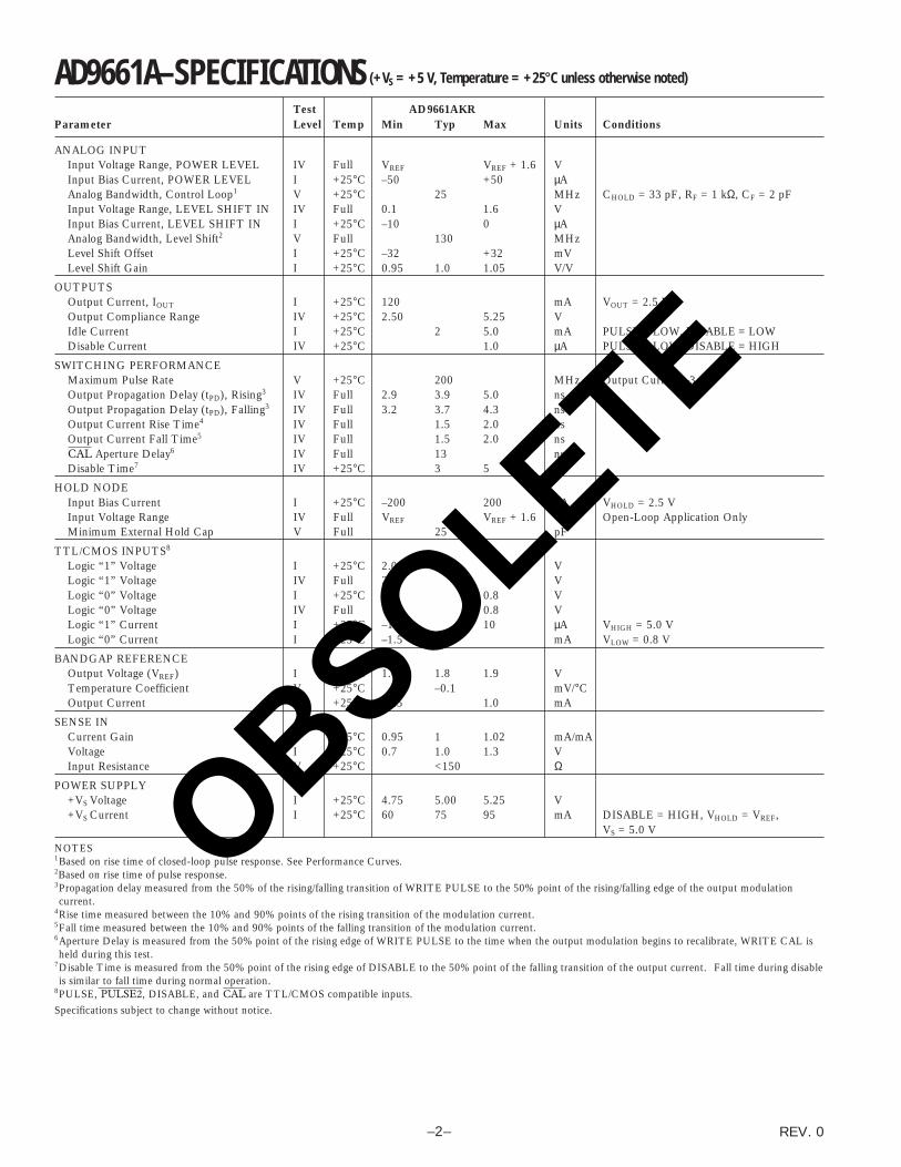
AD9661A–SPECIFICATIONSTest AD9661AKR
Parameter Level Temp Min Typ Max Units Conditions
ANALOG INPUTInput Voltage Range, POWER LEVEL IV Full VREF VREF + 1.6 VInput Bias Current, POWER LEVEL I +25°C –50 +50 µAAnalog Bandwidth, Control Loop1 V +25°C 25 MHz CHOLD = 33 pF, RF = 1 kΩ, CF = 2 pFInput Voltage Range, LEVEL SHIFT IN IV Full 0.1 1.6 VInput Bias Current, LEVEL SHIFT IN I +25°C –10 0 µAAnalog Bandwidth, Level Shift2 V Full 130 MHzLevel Shift Offset I +25°C –32 +32 mVLevel Shift Gain I +25°C 0.95 1.0 1.05 V/V
OUTPUTSOutput Current, IOUT I +25°C 120 mA VOUT = 2.5 VOutput Compliance Range IV +25°C 2.50 5.25 VIdle Current I +25°C 2 5.0 mA PULSE = LOW, DISABLE = LOWDisable Current IV +25°C 1.0 µA PULSE = LOW, DISABLE = HIGH
SWITCHING PERFORMANCEMaximum Pulse Rate V +25°C 200 MHz Output Current –3 dBOutput Propagation Delay (tPD), Rising3 IV Full 2.9 3.9 5.0 nsOutput Propagation Delay (tPD), Falling3 IV Full 3.2 3.7 4.3 nsOutput Current Rise Time4 IV Full 1.5 2.0 nsOutput Current Fall Time5 IV Full 1.5 2.0 nsCAL Aperture Delay6 IV Full 13 nsDisable Time7 IV +25°C 3 5 ns
HOLD NODEInput Bias Current I +25°C –200 200 nA VHOLD = 2.5 VInput Voltage Range IV Full VREF VREF + 1.6 V Open-Loop Application OnlyMinimum External Hold Cap V Full 25 pF
TTL/CMOS INPUTS8
Logic “1” Voltage I +25°C 2.0 VLogic “1” Voltage IV Full 2.0 VLogic “0” Voltage I +25°C 0.8 VLogic “0” Voltage IV Full 0.8 VLogic “1” Current I +25°C –10 10 µA VHIGH = 5.0 VLogic “0” Current I +25°C –1.5 mA VLOW = 0.8 V
BANDGAP REFERENCEOutput Voltage (VREF) I +25°C 1.6 1.8 1.9 VTemperature Coefficient V +25°C –0.1 mV/°COutput Current V +25°C –0.5 1.0 mA
SENSE INCurrent Gain I +25°C 0.95 1 1.02 mA/mAVoltage I +25°C 0.7 1.0 1.3 VInput Resistance V +25°C <150 Ω
POWER SUPPLY+VS Voltage I +25°C 4.75 5.00 5.25 V+VS Current I +25°C 60 75 95 mA DISABLE = HIGH, VHOLD = VREF,
VS = 5.0 V
NOTES1Based on rise time of closed-loop pulse response. See Performance Curves.2Based on rise time of pulse response.3Propagation delay measured from the 50% of the rising/falling transition of WRITE PULSE to the 50% point of the rising/falling edge of the output modulationcurrent.
4Rise time measured between the 10% and 90% points of the rising transition of the modulation current.5Fall time measured between the 10% and 90% points of the falling transition of the modulation current.6Aperture Delay is measured from the 50% point of the rising edge of WRITE PULSE to the time when the output modulation begins to recalibrate, WRITE CAL isheld during this test.
7Disable Time is measured from the 50% point of the rising edge of DISABLE to the 50% point of the falling transition of the output current. Fall time during disableis similar to fall time during normal operation.
8PULSE, PULSE2, DISABLE, and CAL are TTL/CMOS compatible inputs.
Specifications subject to change without notice.
REV. 0–2–
(+VS = +5 V, Temperature = +258C unless otherwise noted)
OBSOLETE
AD9661A
REV. 0 –3–
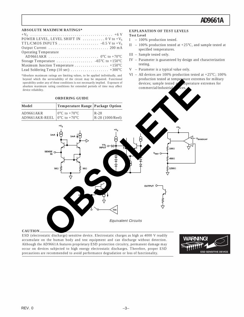
ABSOLUTE MAXIMUM RATINGS*+VS . . . . . . . . . . . . . . . . . . . . . . . . . . . . . . . . . . . . . . . . . +6 VPOWER LEVEL, LEVEL SHIFT IN . . . . . . . . . . . 0 V to +VS
TTL/CMOS INPUTS . . . . . . . . . . . . . . . . . . . . –0.5 V to +VS
Output Current . . . . . . . . . . . . . . . . . . . . . . . . . . . . . . 200 mAOperating Temperature
AD9661AKR . . . . . . . . . . . . . . . . . . . . . . . . . 0°C to +70°CStorage Temperature . . . . . . . . . . . . . . . . . . –65°C to +150°CMaximum Junction Temperature . . . . . . . . . . . . . . . . . +150°CLead Soldering Temp (10 sec) . . . . . . . . . . . . . . . . . . . +300°C*Absolute maximum ratings are limiting values, to be applied individually, andbeyond which the serviceability of the circuit may be impaired. Functionaloperability under any of these conditions is not necessarily implied. Exposure ofabsolute maximum rating conditions for extended periods of time may affectdevice reliability.
ORDERING GUIDE
Model Temperature Range Package Option
AD9661AKR 0°C to +70°C R-28AD9661AKR-REEL 0°C to +70°C R-28 (1000/Reel)
100Ω
450Ω
1250Ω
VBANDGAP
VREF
+VS
1mA
+VS
50Ω 50Ω
SENSEIN
1mA
T/H
HOLD
OUTPUT
TTLINPUT
+VS
Equivalent Circuits
WARNING!
ESD SENSITIVE DEVICE
CAUTIONESD (electrostatic discharge) sensitive device. Electrostatic charges as high as 4000 V readilyaccumulate on the human body and test equipment and can discharge without detection.Although the AD9661A features proprietary ESD protection circuitry, permanent damage mayoccur on devices subjected to high energy electrostatic discharges. Therefore, proper ESDprecautions are recommended to avoid performance degradation or loss of functionality.
EXPLANATION OF TEST LEVELSTest LevelI – 100% production tested.II – 100% production tested at +25°C, and sample tested at
specified temperatures.III – Sample tested only.IV – Parameter is guaranteed by design and characterization
testing.V – Parameter is a typical value only.VI – All devices are 100% production tested at +25°C; 100%
production tested at temperature extremes for militarydevices; sample tested at temperature extremes forcommercial/industrial devices.
OBSOLETE
AD9661A
REV. 0–4–
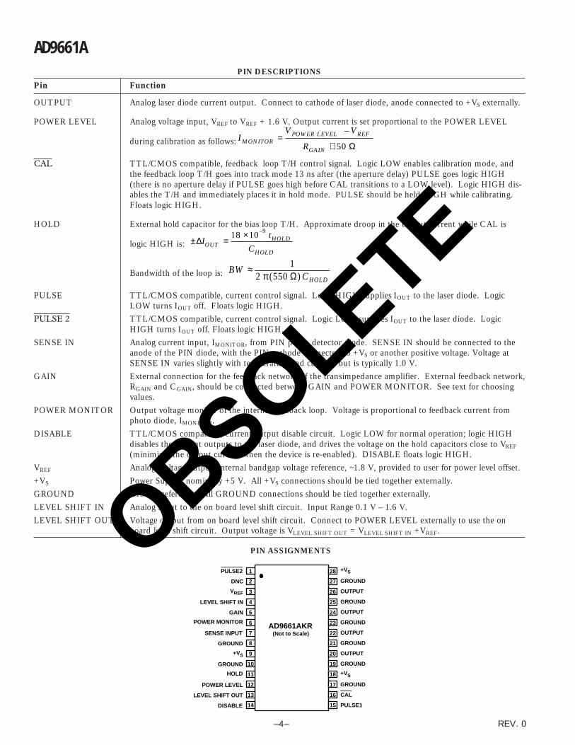
PIN DESCRIPTIONS
Pin Function
OUTPUT Analog laser diode current output. Connect to cathode of laser diode, anode connected to +VS externally.
POWER LEVEL Analog voltage input, VREF to VREF + 1.6 V. Output current is set proportional to the POWER LEVEL
during calibration as follows:
IMONITOR =VPOWER LEVEL – VREF
RGAIN + 50 Ω
CAL TTL/CMOS compatible, feedback loop T/H control signal. Logic LOW enables calibration mode, andthe feedback loop T/H goes into track mode 13 ns after (the aperture delay) PULSE goes logic HIGH(there is no aperture delay if PULSE goes high before CAL transitions to a LOW level). Logic HIGH dis-ables the T/H and immediately places it in hold mode. PULSE should be held HIGH while calibrating.Floats logic HIGH.
HOLD External hold capacitor for the bias loop T/H. Approximate droop in the output current while CAL is
logic HIGH is:
±∆IOUT =18 ×10–9 tHOLD
CHOLD
Bandwidth of the loop is: BW ≈ 1
2 π (550 Ω) CHOLD
PULSE TTL/CMOS compatible, current control signal. Logic HIGH supplies IOUT to the laser diode. LogicLOW turns IOUT off. Floats logic HIGH.
PULSE 2 TTL/CMOS compatible, current control signal. Logic LOW supplies IOUT to the laser diode. LogicHIGH turns IOUT off. Floats logic HIGH.
SENSE IN Analog current input, IMONITOR, from PIN photo detector diode. SENSE IN should be connected to theanode of the PIN diode, with the PIN cathode connected to +VS or another positive voltage. Voltage atSENSE IN varies slightly with temperature and current, but is typically 1.0 V.
GAIN External connection for the feedback network of the transimpedance amplifier. External feedback network,RGAIN and CGAIN, should be connected between GAIN and POWER MONITOR. See text for choosingvalues.
POWER MONITOR Output voltage monitor of the internal feedback loop. Voltage is proportional to feedback current fromphoto diode, IMONITOR.
DISABLE TTL/CMOS compatible, current output disable circuit. Logic LOW for normal operation; logic HIGHdisables the current outputs to the laser diode, and drives the voltage on the hold capacitors close to VREF
(minimizes the output current when the device is re-enabled). DISABLE floats logic HIGH.
VREF Analog Voltage output, internal bandgap voltage reference, ~1.8 V, provided to user for power level offset.
+VS Power Supply, nominally +5 V. All +VS connections should be tied together externally.
GROUND Ground reference. All GROUND connections should be tied together externally.
LEVEL SHIFT IN Analog input to the on board level shift circuit. Input Range 0.1 V – 1.6 V.
LEVEL SHIFT OUT Voltage output from on board level shift circuit. Connect to POWER LEVEL externally to use the onboard level shift circuit. Output voltage is VLEVEL SHIFT OUT = VLEVEL SHIFT IN +VREF.
PIN ASSIGNMENTS
AD9661AKR
1
2
3
4
5
6
7
8
9
10
11
12
13
14
(Not to Scale)
28
27
26
25
24
23
22
21
20
19
18
17
16
15
PULSE2
DNC
VREF
LEVEL SHIFT IN
GAIN
SENSE INPUT
GROUND
+VS
GROUND
HOLD
POWER LEVEL
DISABLE
+VS
GROUND
OUTPUT
GROUND
OUTPUT
GROUND
OUTPUT
GROUND
OUTPUT
GROUND
+VS
GROUND
CAL
PULSE1
POWER MONITOR
LEVEL SHIFT OUT
OBSOLETE
AD9661A
REV. 0 –5–
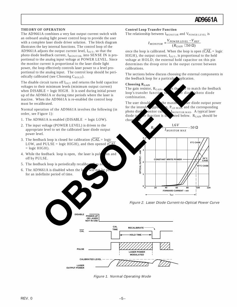
THEORY OF OPERATIONThe AD9661A combines a very fast output current switch withan onboard analog light power control loop to provide the userwith a complete laser diode driver solution. The block diagramillustrates the key internal functions. The control loop of theAD9661A adjusts the output current level, IOUT, so that thephoto diode feedback current, IMONITOR, into SENSE IN is pro-portional to the analog input voltage at POWER LEVEL. Sincethe monitor current is proportional to the laser diode lightpower, the loop effectively controls laser power to a level pro-portional to the analog input. The control loop should be peri-odically calibrated (see Choosing CHOLD).
The disable circuit turns off IOUT and returns the hold capacitorvoltages to their minimum levels (minimum output current)when DISABLE = logic HIGH. It is used during initial powerup of the AD9661A or during time periods where the laser isinactive. When the AD9661A is re-enabled the control loopmust be recalibrated.
Normal operation of the AD9661A involves the following (inorder, see Figure 1):
1. The AD9661A is enabled (DISABLE = logic LOW).
2. The input voltage (POWER LEVEL) is driven to theappropriate level to set the calibrated laser diode outputpower level.
3. The feedback loop is closed for calibration (CAL = logicLOW, and PULSE = logic HIGH), and then opened (CAL= logic HIGH).
4. While the feedback loop is open, the laser is pulsed on andoff by PULSE.
5. The feedback loop is periodically recalibrated as needed.
6. The AD9661A is disabled when the laser will not be pulsedfor an indefinite period of time.
Control Loop Transfer FunctionThe relationship between IMONITOR and VPOWER LEVEL is
IMONITOR =
VPOWER LEVEL –VREF
(RGAIN +50 Ω)
once the loop is calibrated. When the loop is open (CAL = logicHIGH), the output current, IOUT, is proportional to the heldvoltage at HOLD; the external hold capacitor on this pindetermines the droop error in the output current betweencalibrations.
The sections below discuss choosing the external components inthe feedback loop for a particular application.
Choosing RGAIN
The gain resistor, RGAIN, allows the user to match the feedbackloop’s transfer function to the laser diode/photo diodecombination.
The user should define the maximum laser diode output powerfor the intended application, PLD MAX, and the correspondingphoto diode monitor current, IMONITOR MAX. A typical laserdiode transfer function is illustrated below. RGAIN should bechosen as:
RGAIN =
1.6VIMONITOR MAX
–50 Ω
4
3
0
2
1
0 12020 40 60 80 100
OP
TIC
AL
OU
TPU
T –
mW
CONSTANT WRITE POWER
0°C CASE
25°CCASE
50°C CASE
IOUT
FORWARD CURRENT – mA
Figure 2. Laser Diode Current-to-Optical Power Curve
POWER-UPOR LASER
NOT IN USE
CALTIME
RECALIBRATE
LASER POWERMODULATED
DISABLE
CAL
PULSE
LASEROUTPUT POWER
CALIBRATED LEVEL
HOLD TIME
Figure 1. Normal Operating Mode
OBSOLETE
AD9661A
REV. 0–6–
To choose a value, the user will need to determine the amountof time the loop will be in hold mode, t HOLD, the maximumchange in laser output power the application can tolerate, andthe laser efficiency (defined as the change in laser output powerto the change in laser diode current). As an example, if an ap-plication requires 5 mW of laser power ±5%, and the laser diodeefficiency is 0.25 mW/mA, then
∆IMAX = 5mW ×(5%)/ 0.25
mWmA
=1.0mA
If the same application had a hold time requirement of 250 µs,then the minimum value of the hold capacitor would be:
CHOLD =
18 ×10–9 ×250 µs1.0mA
= 4.5nF
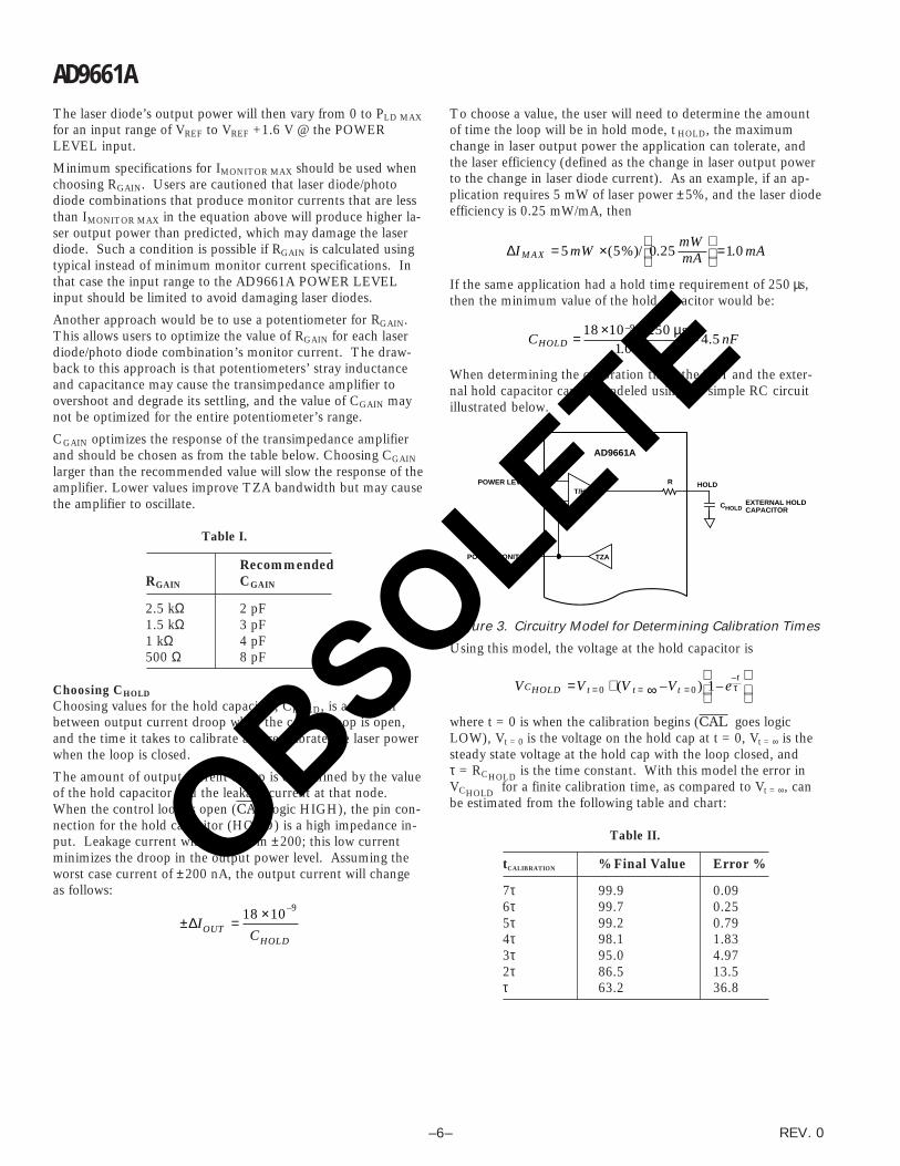
When determining the calibration time, the T/H and the exter-nal hold capacitor can be modeled using the simple RC circuitillustrated below.
CHOLD
R
AD9661A
T/H
TZA
POWER LEVEL
POWER MONITOR
HOLD
EXTERNAL HOLDCAPACITOR
Figure 3. Circuitry Model for Determining Calibration Times
Using this model, the voltage at the hold capacitor is
VCHOLD =Vt = 0 +(Vt = ∞ –Vt = 0) 1– e
–tτ
where t = 0 is when the calibration begins (CAL goes logicLOW), Vt = 0 is the voltage on the hold cap at t = 0, Vt = ∞ is thesteady state voltage at the hold cap with the loop closed, andτ = RCHOLD is the time constant. With this model the error inVCHOLD for a finite calibration time, as compared to Vt = ∞, canbe estimated from the following table and chart:
Table II.
tCALIBRATION % Final Value Error %
7τ 99.9 0.096τ 99.7 0.255τ 99.2 0.794τ 98.1 1.833τ 95.0 4.972τ 86.5 13.5τ 63.2 36.8
The laser diode’s output power will then vary from 0 to PLD MAX
for an input range of VREF to VREF +1.6 V @ the POWERLEVEL input.
Minimum specifications for IMONITOR MAX should be used whenchoosing RGAIN. Users are cautioned that laser diode/photodiode combinations that produce monitor currents that are lessthan IMONITOR MAX in the equation above will produce higher la-ser output power than predicted, which may damage the laserdiode. Such a condition is possible if RGAIN is calculated usingtypical instead of minimum monitor current specifications. Inthat case the input range to the AD9661A POWER LEVELinput should be limited to avoid damaging laser diodes.
Another approach would be to use a potentiometer for RGAIN.This allows users to optimize the value of RGAIN for each laserdiode/photo diode combination’s monitor current. The draw-back to this approach is that potentiometers’ stray inductanceand capacitance may cause the transimpedance amplifier toovershoot and degrade its settling, and the value of CGAIN maynot be optimized for the entire potentiometer’s range.
CGAIN optimizes the response of the transimpedance amplifierand should be chosen as from the table below. Choosing CGAIN
larger than the recommended value will slow the response of theamplifier. Lower values improve TZA bandwidth but may causethe amplifier to oscillate.
Table I.
RecommendedRGAIN CGAIN
2.5 kΩ 2 pF1.5 kΩ 3 pF1 kΩ 4 pF500 Ω 8 pF
Choosing CHOLD
Choosing values for the hold capacitor, CHOLD, is a tradeoffbetween output current droop when the control loop is open,and the time it takes to calibrate and recalibrate the laser powerwhen the loop is closed.
The amount of output current droop is determined by the valueof the hold capacitor and the leakage current at that node.When the control loop is open (CAL logic HIGH), the pin con-nection for the hold capacitor (HOLD) is a high impedance in-put. Leakage current will range from ±200; this low currentminimizes the droop in the output power level. Assuming theworst case current of ±200 nA, the output current will changeas follows:
±∆IOUT =18 ×10–9
CHOLD
OBSOLETE
AD9661A
REV. 0 –7–
TIME CONSTANTS – t
100
30
00 51
% F
INA
L V
ALU
E –
% o
f Vol
ts
2 4
20
10
3
40
50
60
70
80
90
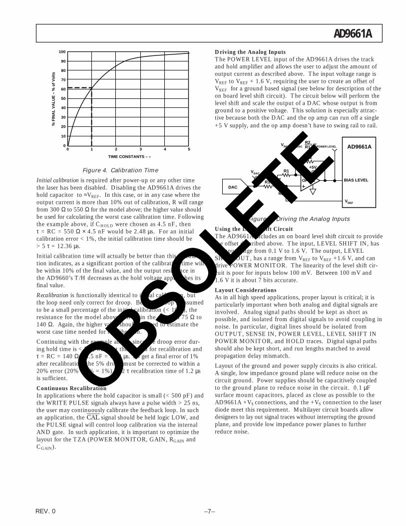
Figure 4. Calibration Time
Initial calibration is required after power-up or any other timethe laser has been disabled. Disabling the AD9661A drives thehold capacitor to ≈VREF. In this case, or in any case where theoutput current is more than 10% out of calibration, R will rangefrom 300 Ω to 550 Ω for the model above; the higher value shouldbe used for calculating the worst case calibration time. Followingthe example above, if CHOLD were chosen as 4.5 nF, thenτ = RC = 550 Ω × 4.5 nF would be 2.48 µs. For an initialcalibration error < 1%, the initial calibration time should be> 5 τ = 12.36 µs.
Initial calibration time will actually be better than this calcula-tion indicates, as a significant portion of the calibration time willbe within 10% of the final value, and the output resistance inthe AD9660’s T/H decreases as the hold voltage approaches itsfinal value.
Recalibration is functionally identical to initial calibration, butthe loop need only correct for droop. Because droop is assumedto be a small percentage of the initial calibration (< 10%), theresistance for the model above will be in the range of 75 Ω to140 Ω. Again, the higher value should be used to estimate theworst case time needed for recalibration.
Continuing with the example above, since the droop error dur-ing hold time is < 5%, we meet the criteria for recalibration andτ = RC = 140 Ω × 4.5 nF = 0.64 µs. To get a final error of 1%after recalibration, the 5% droop must be corrected to within a20% error (20% × 5% = 1%). A 2 τ recalibration time of 1.2 µsis sufficient.
Continuous RecalibrationIn applications where the hold capacitor is small (< 500 pF) andthe WRITE PULSE signals always have a pulse width > 25 ns,the user may continuously calibrate the feedback loop. In suchan application, the CAL signal should be held logic LOW, andthe PULSE signal will control loop calibration via the internalAND gate. In such application, it is important to optimize thelayout for the TZA (POWER MONITOR, GAIN, RGAIN andCGAIN).
Driving the Analog InputsThe POWER LEVEL input of the AD9661A drives the trackand hold amplifier and allows the user to adjust the amount ofoutput current as described above. The input voltage range isVREF to VREF + 1.6 V, requiring the user to create an offset ofVREF for a ground based signal (see below for description of theon board level shift circuit). The circuit below will perform thelevel shift and scale the output of a DAC whose output is fromground to a positive voltage. This solution is especially attrac-tive because both the DAC and the op amp can run off a single+5 V supply, and the op amp doesn’t have to swing rail to rail.
DAC
VDAC
OP191
+5V
VREF + VDAC = VPOWER LEVELR2R1
BIAS LEVEL
VREF
AD9661A
R1
R1
R2
R2
Figure 5. Driving the Analog Inputs
Using the Level Shift CircuitThe AD9661A includes an on board level shift circuit to providethe offset described above. The input, LEVEL SHIFT IN, hasan input range from 0.1 V to 1.6 V. The output, LEVELSHIFT OUT, has a range from VREF to VREF +1.6 V, and candrive POWER MONITOR. The linearity of the level shift cir-cuit is poor for inputs below 100 mV. Between 100 mV and1.6 V it is about 7 bits accurate.
Layout ConsiderationsAs in all high speed applications, proper layout is critical; it isparticularly important when both analog and digital signals areinvolved. Analog signal paths should be kept as short aspossible, and isolated from digital signals to avoid coupling innoise. In particular, digital lines should be isolated fromOUTPUT, SENSE IN, POWER LEVEL, LEVEL SHIFT INPOWER MONITOR, and HOLD traces. Digital signal pathsshould also be kept short, and run lengths matched to avoidpropagation delay mismatch.
Layout of the ground and power supply circuits is also critical.A single, low impedance ground plane will reduce noise on thecircuit ground. Power supplies should be capacitively coupledto the ground plane to reduce noise in the circuit. 0.1 µFsurface mount capacitors, placed as close as possible to theAD9661A +VS connections, and the +VS connection to the laserdiode meet this requirement. Multilayer circuit boards allowdesigners to lay out signal traces without interrupting the groundplane, and provide low impedance power planes to furtherreduce noise.
OBSOLETE
AD9661A
REV. 0–8–
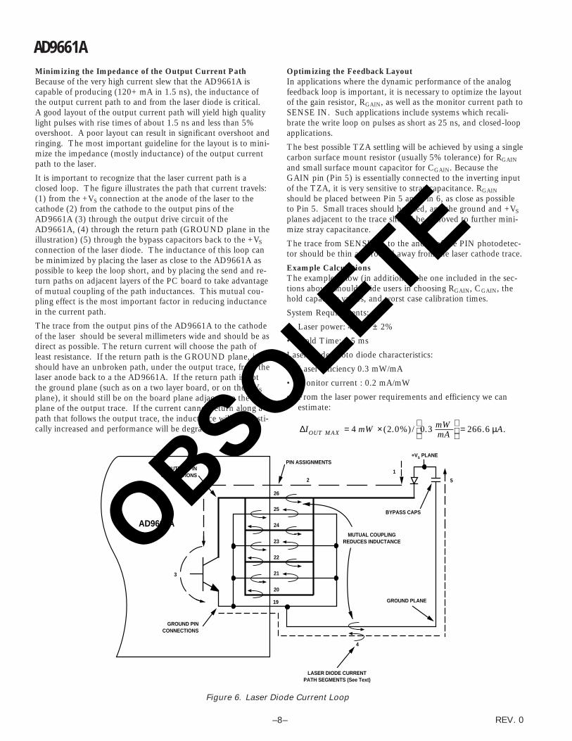
Minimizing the Impedance of the Output Current PathBecause of the very high current slew that the AD9661A iscapable of producing (120+ mA in 1.5 ns), the inductance ofthe output current path to and from the laser diode is critical.A good layout of the output current path will yield high qualitylight pulses with rise times of about 1.5 ns and less than 5%overshoot. A poor layout can result in significant overshoot andringing. The most important guideline for the layout is to mini-mize the impedance (mostly inductance) of the output currentpath to the laser.
It is important to recognize that the laser current path is aclosed loop. The figure illustrates the path that current travels:(1) from the +VS connection at the anode of the laser to thecathode (2) from the cathode to the output pins of theAD9661A (3) through the output drive circuit of theAD9661A, (4) through the return path (GROUND plane in theillustration) (5) through the bypass capacitors back to the +VS
connection of the laser diode. The inductance of this loop canbe minimized by placing the laser as close to the AD9661A aspossible to keep the loop short, and by placing the send and re-turn paths on adjacent layers of the PC board to take advantageof mutual coupling of the path inductances. This mutual cou-pling effect is the most important factor in reducing inductancein the current path.
The trace from the output pins of the AD9661A to the cathodeof the laser should be several millimeters wide and should be asdirect as possible. The return current will choose the path ofleast resistance. If the return path is the GROUND plane, itshould have an unbroken path, under the output trace, from thelaser anode back to a the AD9661A. If the return path is notthe ground plane (such as on a two layer board, or on the +VS
plane), it should still be on the board plane adjacent to theplane of the output trace. If the current cannot return along apath that follows the output trace, the inductance will be drasti-cally increased and performance will be degraded.
GROUND PLANE
BYPASS CAPS
GROUND PINCONNECTIONS
OUTPUT PINCONNECTIONS
PIN ASSIGNMENTS
LASER DIODE CURRENTPATH SEGMENTS (See Text)
25
24
23
22
21
20
19
MUTUAL COUPLINGREDUCES INDUCTANCE
4
52
1
3
AD9661A
26
+VS PLANE
Figure 6. Laser Diode Current Loop
Optimizing the Feedback LayoutIn applications where the dynamic performance of the analogfeedback loop is important, it is necessary to optimize the layoutof the gain resistor, RGAIN, as well as the monitor current path toSENSE IN. Such applications include systems which recali-brate the write loop on pulses as short as 25 ns, and closed-loopapplications.
The best possible TZA settling will be achieved by using a singlecarbon surface mount resistor (usually 5% tolerance) for RGAIN
and small surface mount capacitor for CGAIN. Because theGAIN pin (Pin 5) is essentially connected to the inverting inputof the TZA, it is very sensitive to stray capacitance. RGAIN
should be placed between Pin 5 and Pin 6, as close as possibleto Pin 5. Small traces should be used, and the ground and +VS
planes adjacent to the trace should be removed to further mini-mize stray capacitance.
The trace from SENSE IN to the anode of the PIN photodetec-tor should be thin and routed away from the laser cathode trace.
Example CalculationsThe example below (in addition to the one included in the sec-tions above) should guide users in choosing RGAIN, CGAIN, thehold capacitor values, and worst case calibration times.
System Requirements:
• Laser power: 4 mW ± 2%
• Hold Time: 0.5 ms
Laser diode/photo diode characteristics:
• Laser efficiency 0.3 mW/mA
• Monitor current : 0.2 mA/mW
• From the laser power requirements and efficiency we canestimate:
∆IOUT MAX = 4 mW × (2.0%)/ 0.3 mW
mA
= 266.6 µA.
OBSOLETE
AD9661A
REV. 0 –9–
• Choosing a hold caps based on this:
CHOLD =
18 ×10–9 ×0.5ms266.6 µA
= 0.034 µF
• The initial calibration time for < 0.1% error:
7 τ = 7 × RC = 7 × 550 Ω × 0.034 µF = 130.9 µs
• Recalibration for a 0.1% error after 2% droop (need tocorrect within 5%):
3 τ = 3 RC = 3 × 140 Ω × 0.034 µF = 14.28 µs
• From the monitor current specification and the max powerspecified:
IMONITOR MAX = 4 mW
0.2 mA
mW= 800 µA
and
RGAIN =1.6V
IMONITOR MAX
– 50 Ω = 2.0 kΩ
• CGAIN would be chosen from the table as 3 pF for safecompensation.
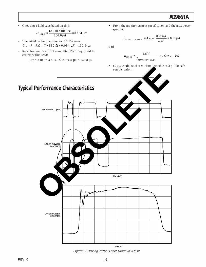
1ns/DIV
20ns/DIV
PULSE INPUT (TTL)
LASER POWER20mV/DIV
LASER POWER20mV/DIV
Figure 7. Driving 78N20 Laser Diode @ 5 mW
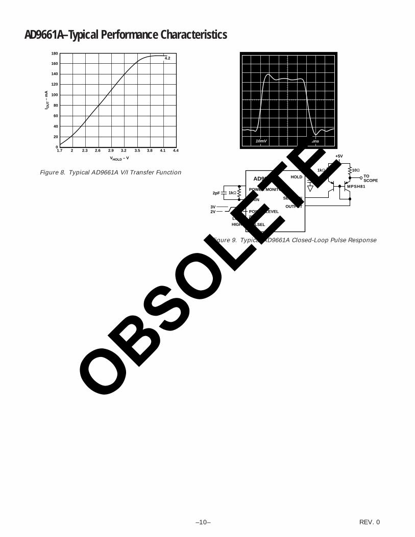
Typical Performance Characteristics
OBSOLETE
20ns10mV
+5V
1kΩ 10ΩTOSCOPE
MPSH8133pF
HOLD
SENSE IN
OUTPUT
AD9661A
POWER MONITOR
GAIN
POWER LEVEL
PULSEL
LOWHIGH
3V2V
2pF 1kΩ
Figure 9. Typical AD9661A Closed-Loop Pulse Response
VHOLD – V
180
40
01.7 3.22
I OU
T –
mA
2.3 2.9
20
2.6
60
80
100
120
140
160
3.5 3.8 4.1 4.4
4.2
Figure 8. Typical AD9661A V/I Transfer Function
AD9661A–Typical Performance Characteristics
REV. 0–10–
OBSOLETE
AD9661A
REV. 0 –11–
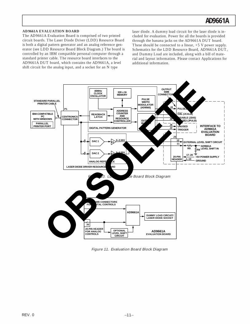
AD9661A EVALUATION BOARDThe AD9661A Evaluation Board is comprised of two printedcircuit boards. The Laser Diode Driver (LDD) Resource Boardis both a digital pattern generator and an analog reference gen-erator (see LDD Resource Board Block Diagram.) The board iscontrolled by an IBM compatible personal computer through astandard printer cable. The resource board interfaces to theAD9661A DUT board, which contains the AD9661A, a levelshift circuit for the analog input, and a socket for an N type
laser diode. A dummy load circuit for the laser diode is in-cluded for evaluation. Power for all the boards is providedthrough the banana jacks on the AD9661A DUT board.These should be connected to a linear, +5 V power supply.Schematics for the LDD Resource Board, AD9661A DUT,and Dummy Load are included, along with a bill of mate-rial and layout information. Please contact Applications foradditional information.
Figure 10. LDD Resource Board Block Diagram
AD9661ADUMMY LOAD CIRCUIT/LASER DIODE SOCKET
OPTIONALLEVEL SHIFT
CIRCUIT
AD9661AEVALUATION BOARD
20
5
INPUT SMB CONNECTORSFOR DIGITAL CONTROLS
20-PIN HEADERFOR ANALOGCONTROLS
Figure 11. Evaluation Board Block Diagram
40MHzCLOCK
OSCILLATOR
32K x 16MEMORY
OUTPUTSMB
CONNECTORS
ADDRESSCOUNTER
ANDRESOURCE
CONTROLLER
READBACKLATCH
DIGITAL PATTERN GENERATOR
CENTRONICSCONNECTOR
P1
STANDARD PARALLELPRINTER CABLE
IBM-COMPATIBLEPC
WITH WINDOWS
PARALLELPRINTER PORT
8
8X1
X1
0–2.55V
0–2.55V
ANALOG REFERENCE
LASER DIODE DRIVER RESOURCE BOARD
J4
J5J7J8
J6J2
CAL (JCALB)
DISABLE (JDIS)PULSE2 (JPULB)
UNUSEDTRIGGER
PULSE1 (JPUL)
20-PINHEADER
J31211
R9 R8
AD9661ALEVEL SHIFT IN
+5V POWER SUPPLY
GROUND
17–20
1–10
EXTERNAL LEVEL SHIFT CIRCUIT
PULSEWIDTH
MODULATOR(AD9560)
OUTPUTBUFFER
INTERFACE TOAD9661A
EVALUATIONBOARD
DAC 1
DAC 2
OBSOLETE
AD9661A
REV. 0–12–
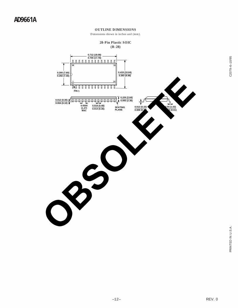
OUTLINE DIMENSIONSDimensions shown in inches and (mm).
28-Pin Plastic SOIC(R-28)
28 15
141
0.712 (18.08)0.700 (17.78)
0.419 (10.64)0.393 (9.98)
0.300 (7.60)0.292 (7.40)
PIN 1
SEATINGPLANE
0.012 (0.30)0.004 (0.10)
0.019 (0.48)0.014 (0.36)
0.104 (2.64)0.093 (2.36)
0.0500(1.27)BSC
0.013 (0.33)0.009 (0.23)
0.04 (1.02)0.024 (0.61)
C20
79–6
–10/
95P
RIN
TE
D IN
U.S
.A.OBSOLETE