Embed Size (px)
Citation preview


Laporan Akhir Projek PenyelidikanJangka Pendek
Investigation of Low Dielectric Constant(k) Films for Deep Sub-Micron CMOS
Application
byIr. Dr. Cheon'g Kuan Yew
Assoc. Prof. Dr. Luay Bakir Hussain

IlJb11IUNIVERSITI SAINS MALAYSIA
LAPORAN AKHIR PROJEK PENYELIDlKAN JANGKA PENDEKFINAL REPORT OF SHORT TERM RESEARCH PROJECTSila kemukakan laporan akhir ini melalui lawatankuasa Penyelidikan di PusatPengajian dan DekanIPengarahlKetua labatan kepada Pejabat Pelantar Penyelidikan
1. Nama Ketua Penyelidik: Ir. Cheong Kuan YewName ofResearch Leadero Profesor Madya! !Zl Dr.! o EncikIPuan/Cik
Assoc. Prof Dr. Mr/Mrs/Ms
2. Pusat Tanggungjawab (PTJ):School/Department
School of Materials & Mineral Resources Engineering
3. Nama Penyelidik Bersama:Name ofeo-Researcher
Assoc. Prof. Dr. Luay Bakir Hussain
4. Tajuk Projek:Title ofProject
OLD TITLE: Development of localized-selective-stress etch-stop layer (ESL) for a ne~
CMOS integration schemeNEW TITLE: Investigation of low dielectric constant (k) films for deep sub-micron CMOSapplication.
5. Ringkasan Peniiaian/Summary ofAssessment: Tidak Boleh 5aogat Baik 'Mencukupi Diterima Very GoodInadequate Acceptable
I 2 3 4 5
i) Pencapaian objektif projek: D D D [Z] DAchievement ofproject objectives
ii) Kualiti output: D D [Z] D DQuality ofoutputs
'",.iii) Kualiti impak: D D [ZJ D DQuality ofimpacts
iv) Pemindahan teknologi/potensi pengkomersialan: D ~ D D DTechnology transjerlcommercialization potential
,
v) Kualiti dan usahasama : D D D D [ZJQuality and intensity ofcollaboration
vi) Penilaian kepentingan secara keseluruhan: D D [Z] D DOverall assessment ofbenefits

Laporan Akhir Projek Penyelidikan Jangka PendekFinal Report O/Short Term Research Project
6. Abstrak Penyelidikan(Perlu disediakan diantara 100 - 200 perkataan di dalam Bahasa Malaysia dan juga Bahasa Inggeris.Abstrak ini akan dimuatkan dalam Laporan Tahunan Bahagian Penyelidikan & Inovasi sebagai satu carauntuk menyampaikan dapatan projek tuan/puan kepada pihak Universiti & masyarakat luar).
Abstract ofResearch(An abstract ofbetween 100 and 200 words must be prepared in Bahasa Malaysia and in English).This abstract will be included in the Annual Report ofthe Research and Innovation Section at a later date as ameans ofpresenting the projectjindings ofthe researcher/s to the University and the community at large)
Please reter to Appendix A
7. Sila sediakan laporan teknikallengkap yang menerangkan keseluruhan projek ini.ISila gunakan kertas berasingan)Applicant are required to prepare a Comprehensive Technical Report explaning the project.(This report must be appended separately)
A Comprehensive Technical Report is appended separately.
Seriaraikan kata kunci yang mencerminkan penyelidikan anda:List the key words that reflects your research:
Bahasa Malaysia
Pengendapan Sol-gelPemalar dieletrik rendahFilem nipis
8. Output dan Faedah ProjekOutputand Benejits ofProject
Bahasa Inggeris
Sol-gel depositionLow dielectric constantThin tHem
(a) * Penerbitan JurnalPublication ofJournals(Sila nyatakan jenis, tlljuk, pengarang/editor, tabun terbitan dan di mana telab diterbit/diserabkan)(State type, title, author/editor, publication year and where it has been published/submitted)
1. KY. Cheong and F.A. Jasni, "Effect~ of Precursor Aging and Post-DepositionTreatment Time on Photo-assisted Sol-gel Derived Low;,DieJectric Constant Si02 ThinFilm on Si," Microelectronics Journal (Elsevier), vol. 38, pp. 227-230, 2007.
2. W.C. Ee and K. Y.Cheong, "Effects of Annealing Temperature on Low DielectricConstant Si02 Thin Films Derived from Sol-gel Tetraethylorthosilicate andMethyltriethoxysilane Source," Microelectronics Journal (Elsevier) - under review.
2

-.(b)
Laporan Akhir Projek Penyelidikan Jangka PendekFinal Report O/Shorl Term Research Project
Faedah-faedah lain seperti perkembangan produk, pengkomersialan produk/pendaftaran patenatau impak kepada dasar dan masyarakat.State other benefits such as product development. product commercialisation/patent registration or impacton source and society.
The formulation usedto produce the low-k thin film may be employed infuture generation of microelectronic devices. This enables a betterperformance device to be made and eventually quality of life of man-kindcan be improved.
• Sila berikan salinan/Kindlyprovide copies
(c) Latihan Sumber ManusiaTraining in Human Resources
i)Not ApplicablePelajar Sarjana: _
Graduates Students(Perincikan nama, ijazah dan status)(Provide names, degrees and status)
ii) Lain-lain:Others
Undergraduate (Final Year Project) - 2 students• 2005/2006: Ms Farah Anis binti Jasni• 2006/2007: Mr Ee Woei Chang
Research Assistant - 1 student• July 2006 - Oct 2006: Ms Khor Siew Cheng
9. Peralatan yang Telah Dibeli:Equipment that has been purchased
No equipment is purchased unger this grant.
~
IR. DR. CHEONG AN YEWPCllsyarahP.P. Kejuruterwl Baban & Somber MineraiKampus Kejuroteraal1llllivcrsiti Sains Malaysia
Tandatangan PenyelidikSignature ofResearcher
3
22 June 2007
TarikhDate

Komen Jawatankuasa Penyelidikan Pusat Pengajian/PusatComments by the Research Committees ofSchools/Centres
Laporan Akhir Projek Penyelidikan Jangka PendekFinal Report a/Short Term Research Project
,..•
TAN ANGAN PENGERUSIJAWATANKUASA PENYELIDlKAN
PUSAT PENGAJIAN/PUSATSignature ofChairman
[Research Committee ofSchool/Centre}
4
TarikhDate

Appendix A
English Abstract:
Silica (Si02) thin film on Si with low dielectric constant (k) properties has beensystematically prepared and investigated. Two types of this low-k material have beendeposited on Si via sol-gel spin-on coating. Tetraethylorthosilicate (TEOS) was used as aprecursor to produce the first type of film. The effects of precursor aging (0, 2, 4, and 6days) and post-deposition treatment time (0, 1, 2, 3 h) on photo-assisted condition havebeen investigated. The other type of film was derived from a mixture of TEOS andmethyltriethoxysilane (MTES). Different molar ratio of TEOS/MTES (1: 1, 2: 1 4:1 and 6:1)and post deposition annealing condition (300-500oC for 30 minutes in argon) have beeninvestigated. The physical properties of the dielectric film was characterized using Filmetric,fourier transform infrared spectroscopy, X-ray diffraction, atomic force microscope (AFM),and scanning electron microscope; while the electrical properties were investigated byconductive AFM and a semiconductor parameter analyzer. The best film derived fromTEOS alone was using longest aging time of precursor with longest photo exposure time.Using a mixture of TEOS:MTES=4:1, the derived film with the lowest leakage current and kvalue (1.93) was annealed at 500°C.
Malay Abstract:
Filem nipis silika (Si02) yang berpemalar dieletrik rendah endap di atas Si tlahdisediakan dan dikaji dengan sistematik. Dua jenis film nipis telah disediakan menggunkanpemutaran sol-gel. Tetraethylorthosilicate (TEOS) telah digunakan sebagai prapenandauntuk film jenis pertama. Kesan masa penuaan (0, 2, 4, dan 6 hari) dan rawatan pascapengendapan (0, 1,. 2, 3 jam) ke atas keadaan rawatan foto telah dikaji. Film nipis lagi satutelah disediakan dengan campuran TEOS dan methyltriethoxysilane (MTES). Nisbah molarTEOS/MTES (1:1,2:1 4:1 dan 6:1) dan suhu rawatan pasca pengendapan (300-500°C, 30min. di argon) telah dikaji. Sifat fizikal film telah dicirikan dengan Filmetric, fourier transforminfrared spectroscopy, X-ray diffraction, atomic force microscope (AFM) , dan scanningelectron microscope; manakala sifat elektrik telah dikajikan dengan conductive AFM dansemiconductor parameter analx.zer. Film yang paling bagus disediakan dengan TEOSsahaja ialah daripada prapenanda dan rawatan foto yang palingg lama. Denganmenggunakan prapenanda campuran (4:1) telah menghasilkan film berarus bocor palingrendah dan nilai k (1.93) bila dirawat pada 500°C.
5

ELSEVIER Microelectronics Journal 38 (2007) 227-230
MicroelectronicsJournal
www.elsevier.com/locate/mejo
Effects of precursor aging and post-deposition treatmellt time onphoto-assisted sol-gel derived low-dielectric constant SiQith.ip. film on Si
K.Y. Cheong*, F.A. JasniElectron Materials Research Group, School of Materials & Mineral Resources Engineering, EngineerinQ Cfi!npus, Universili Sains Malaysia,
Seri Ampangan, 14300 Nibong Tebal, Seberang Perai Selatan, PenanwzMalaysia
Received 12 October 2006; accepted 22 November 2006Available online 8 January 2007
Abstract
In this paper, we have reported the results of sol-gel derived low dielectriq;£onstant Si02 treated with UV light as a function ofprecursor aging time and post·deposition UV exposure time. Filmetrics, FO!JJier~ftllnsform infrared, and scanning electron microscopewere employed to characterize the films. Precursor aged for the longest timrJfd\lYs) has demonstrated the lowest refractive index, whichcan be related to reduction of dynamic dielectric constant (ke). Howexer;'f'\\ihen the UV exposure time increased, the ke value alsoincreased. These observations have been explained in the text. ..,>, ...
© 2006 Elsevier Ltd. All rights reserved."::.i:/"
Keywords: Sol-gel; Low-dielectric constant thin film; Fourier-transform il}frared
1. Introduction
The evolution of integrated circuit (IC) devi~$.' isgoverned by Moore's law. It is achieved largely throtlghdie shirks. As the semiconductor node moves from 0.25 Ilmto lower values, a critical point is rel\phed where thereduction in signal propagation delay(otj~t"'dcelay,whereRand C refer to resistance and capll~itan~{respectively)due to a shorter path is offset bYl,I.i;highef resistance ofmetal trace and an increased effe<;~Qr)tl,1e inter and intralayers of insulating dielectrics [l],'\~s~l:!ch, the conventionalthermal growth and chemica aOl'/lleposited Si02 withdielectric constant (k) 0 ,.not able to meet therequirement as inter aog: a-layers of insulating di-electrics. This RC delay carl,; be reduced by loweringthe capacitance, C, value"whereby a lower k material isused [I]. .
Many polymetshaye.geen considered as low-k materials,however, they are having poor thermal stability andmechanical strength [2,3]. Comparatively, sol-gel derivedsilica has demonstrated a better property but their k valuesare not as low as their polymer counterparts [4,5]. In this
·Corresponding author. Tel.: +6045995259; fax: +6045941011.E-mail address:[email protected] (K.Y. Cheong).
00~6-2692/$.see front matter © 2006 Elsevier Ltd. All rights reserved.dOI:10.1016/j.mejo.2oo6.1 1.01 I
project, Si02 thin film with k value lower than theconvention thermal and chemical vapor deposited Si02
will be deposited on silicon (Si) by sol-gel spin-on-coatingand post-deposition treatment under UV light at varioustimes. The morphology and chemical structures of the filmswill be studied.
2. Experimental procedures
Tetraethyl orthosilicate (TEaS), deionized water (01),ethanol, and HCI were used to prepare a crystal clearprecursor for the sol-gel derived Si02 thin films. Firstly, amixture of 12.4 mol ratio of DI:TEOS was prepared understirring condition. An appropriate amount of ethanol was.added to the mixture and then followed by a few drops ofHCI to control pH of the precursor. The precursor wasstirred for 90 min so that hydrolysis could be initiated. Theproduct was then divided into four equal amounts andstored in four diffC1l'ent beakers. The beakers were labeledas A, B, C, and D; indicating the aging time for theprecursor before deposition. The aging time for A, B, C,and D were 0, 2, 4, and 6 days, respectively. Afterunderwent an appropriate aging, the precursor was readyto be applied on a RCA-cleaned Si (I 00) wafer. A spinner

228K. Y. Cheong, F.A. Jasni / Microelectronics Journal 38 (2007) 227-230
was used to perform the spin-on-coating process with aspeed and time of 4000 rpm and 45 s, respectively. Afterspinning, the sample was inserted in a ch~~ber with UVwavelength of 250 nm for the post-deposItIOn treatment.The samples were exposed at the same wavelength fordifferent durations. After the treatment the samples weresent for characterization. The thickness and opticalproperties of the films were examined by a Filmetricssystem. The chemical structure of the films was characterized using a Fourier-transform infrared (FTIR). Scanningelectron microscopy (SEM, SUPRA-35VP) was utilized toinvestigate the morphology of the films.
3. Results and discussion
Contrary, the n value decreases dramatically as the agingtime of the precursor increases. Since the polymerizationmay initiate after a period of aging, the chemical structurescould become larger than non-aged precursor. Thissuggests that the reduction of n value is most probablyattributed to the change of chemical structures that mayinduce pores in the film.
The dynamic dielectric constant (k.) of these films hasbeen investigated at UV-visible rartgeusing a Filmetricssystem at wavelength of 632.81111'it·The squared of the nvalue obtained from this wavelength;provides the ke value(Fig. 3) as shown in Eq. (1). Jhetrendofke as a function ofUV exposure time and prec~J~Qrjaging time are similar toFig.2." .'
Fig. 2. Refractive index as a function of UV exposure lime for samplesprepared from precursor aged at different period.
Fig. 4 reveals the FTIR spectra for the Si02 thin filmprepared fromPf<;fursor aged for 4 days and treated under
1.44
(1 )
3
_ Oday
2 days
.;...
1 2 .
UV Exposure Time (h)
i... ... ..- ...-- ~ ".
o1.34
1.42
1.36
~~ 1.40
.~,'0
x; ~ 1.38·····.· ........ 5-."'""':c ........ ·T ..,,£
Sample D that has been aged for 6 days has fullytransformed into gel form. Therefore, it could not be usedin the subsequent process. Fig. I shows the result of oxidethickness as a function of UV exposure time for the threetypes of samples (A, B, and C). As UV exposure timeincreases, the oxide thickness decreases but the changes aresmall. This indicates that densification of the gel to solidstate occurs as UV exposure time increases. In contrast,oxide thickness significantly increases as the aging time ofthe precursor increases from 0 to 4 days. This is probablydue to the increase of polymerization of the precursor asthe aging time increases and attribute to a more viscousprecursor.
Fig. 2 presents the refractive index (n) of the thin film asa function of UV exposure time. All of the san1pI~~{xrevealed n value lower than the conventional thermal/addchemical vapor deposited Si02 films (n = 1.46)."'q'\}it;indicates that the sol-gel derived Si02 film in this wofkiprobably has a larger porosity or larger chemical structures. This may imply that the dielectric constant (k) of thethin film is also relatively smaller t4an;i;tl1e<Si02 filmprepared by conventional methods. Ast:JV~~pl:lsure timeincreases, n value also demonstrated ari incr~asing trend.
600 .--- ----...,.....-----,..--.....,
012 3
UV Exposure TIme (h)
Fig. I. Oxide Ihickness as a function of UV exposure lime for samplesprepared from precursor aged at different period.
31 2
UV Exposure Time (h)
o
....... ..;. ,..
4daysf--
Aging Time
1.80
1.85
2.00.:1"i~ 1.95l5u(,l
is' 1.90Q)
Giis
Fig. 3. Dynamic dielectric conslant as a function of UV exposure time forsamples prepared from precursor aged al different period.
2.05 r---~--"""----""------'
... ~. ... --t 4 days
! 1. '-~i.!------of Oday
............~=4E 550
S.
J 500iii'"CIl 450c
~ 400QI1:1'5(0 350
300

K. 1'. Cheong, F.A. Jasni / Microelectronics Journal 38 (2007) 227-230 229
_··..··:ll·-:.r..~····_·_····_·····;:I;:l····· ..·....-.-.----:I~:- ...""f';'~"~L'" -~- 23111.7t "t """'T'"
3131.5.S ssti 2111.'4 '543.1'
'''' ,.......
I 2h
.- (, _.-'"'' -r-I--'\'1 _.."'''''''' I I "51' In.. \~ ......\.1 MUI nU3 ISl047 ~~~
I --'y'-' / 3h10.......""./""., / \"
lotlOl 7'lU7 I610.01 451.54
4000.0 3600 3200 2800 24000 2000 1800 1600 1400 12qQ <"IqQO 800 600 400.0
Wave number (em· l )
Fig. 4. A comparison of FTIR spectra for samples prepared from precursor aged for;,:4d.a,~~ '(teated at different UV exposure time and thermal Si02
sample. """
Fig. 5. SEM micrographs qf:.~aJyples prepared from precursor aged for 4 days and treated at (a) 0 and (b) 3 h of UV light.,-·----::~x~
UV light at different dUJ;aHohs. These spectra are alsocompared with a spectrttnl;obtained from a conventionalthermal Si02 thin!iJ1;ll. 'Pr6m the spectra, individual peakswith wave number$~~ve'been included. Peaks representingSi02 structures ana/the mode of the structures have alsobeen included for comparison. Besides having stretchingmode of Si-O-Si, rocking (454cm- l
) and bending(739cm- l
) modes of Si-O-Si were also observed in thesol-gel derived Si02 films. A shoulder at l200cm- 1 is alsobeing observed in all the spectra of the investigated films.This shoulder indicates an increase of stretch in Si-Q-Si ofthis films if compared with the conventional Si02 film [6].Some reports also suggested that the appearance of this
shoulder may attribute to the decrease of refractive index(n) [6]. This conclusion is in agreement with the observationobtained in this work. In general, the shape of the FTIR1>pectra of the remaining two samples (aged at 0 and 2 days)are almost similar to Fig. 4.
Fig. 5(a) and (b) compares the SEM micrographs of thesol-gel derived Si02 films prepared from precursor aged for4 days. The non-UV treated film (Fig. 5(a» shows arandom microcrack on the film surface. After the UVtreatment, the cracks have been reduced significantly. Theactual reason for this reduction has yet been investigated.The most probable explanation of this observation may bedue to the breaking of huge chemical structures derived

230 K. Y. Cheong, F.A. Jasni / Microelectronics Journal 38 (2007) 227-230
from the long aging time of the precursor. After thisbreaking process, UV may also be introduced to enhancethe drying process of the film.
4. Conclusions
The effect of precursor aging time and of post-depositionUV exposure time of sol-gel derived low dielectric constantSiOz have been il,lVestigated and reported in this paper.Optical properties, chemical structures, and film morphology have been studied. Samples prepared from precursoraged for the longest time revealed the lowest dynamicdielectric constant. This constant was increased when UVexposure time increased. These observations have beenexplained in the text.
References
[I) S. Wolf, Silicon Processing for the VLSI Era, Vol. 4-DeepSubmicron Process Technology, Lattice Press, California, 2002, pp.639-670.
[21 B.D. Hatton, K. Landskron, W.J. Hunks, M.R. Bennett, D. Shukaris,D.O. Perovic, G.A. Ozin, Mater. Today 9 (2006) 22.
[3) L. Shen, K. Zeng, Microelectron. Eng. 71 (2004) 221.[4) L.W. Hrubesh, J. Non-Crysl. Solids 225 (1998) 335.[5) F. Blaschta, K. Schulze, S.E. Schulz, T.Oess.~er, Microelectron. Eng.
76 (2004) 8. . .[6) W.S. Lau, Infrared Characteristic f()T MICroelectronic, World Scien
tific Publishing, Singapore, 1999, pp.5,§,-S7.

Effects of Annealing Temperature on Low Dielectric Constant Si02 Thin Films
Derived from Sol-gel Tetraethylorthosilicate and Methyltriethoxysilane Source
Woei Chang Ee and Kuan Yew Cheong*
Electronic Materials Research Group, School of Materials & Mineral Resources
Engineering, Engineering Campus, Universiti Sains Malaysia, 14300 Nibong Tebal,
Seberang Perai Selatan, Penang, Malaysia.
*e-mail: [email protected]
Abstract
The results of low dielectric constant (k) Si02 films derived from sol-gel spin-
on coating process using a combination of tetraethylorthosilicate (TEOS) and
methyltriethoxysilane (MTES) (mole ratio of TEOS:MTES = 4: 1) have been reported.
The effects of post deposition annealing temperature (300 to 500°C for 30 min in argon
ambient) 0 n the p hysical, chemical, and electrical properties of t he oxide have been
systematically investigated. Filmetric system, Fourier transform infrared spectroscope,
x-ray diffraction system, atomic force microscope, and field-emission scanning electron
microscope with energy gispersive x-ray have been employed for physical and
chemical analyses. Electrical property of the oxide, in terms of leakage current through
the oxide, has also been investigated. The oxide annealed at 500°C produced the
lowest dielectric constant value (k=2.3) and the lowest leakage current with no obvious
oxide breakdown. The explanation of this observation has been discussed.,

1. Introduction
The growth of integrated circuit technology is primarily based on the ability of
minimum feature size in the circuits to continue shrink down to deep submicron region.
Smaller devices give higher packing density as well as higher operating speeds.
However, with a higher device speed, there is an almost inevitable need to reduce RC
delay in multilevel interconnections; where Rand C are resistance and capacitance,
respectively. This RC delay can either be reduced by lowering R value of metal
interconnect, w hereby aluminum is replaced by c opper, and/or C value of i nterlayer
dielectric (ILD), whereby a conventional oxide is replaced by a lower k material [1,2].
A variety of low k materials have been reported, such as non-fluorinated
polymers, organic polymer, and silica (Si02) [2,3]. Among these materials, low-k Si02
has demonstrated a more structural and thermal stable film than others [2]. Many
techniques have been used to produce Si02-based low k materials. Sol-gel spin-on
coating is appeared to be a more extendible method as it is able to fill various aspect
ratio of interconnects and produce porous structures that can further lower the k value
(1.3-2.5) [2-5]. Although a lower k value of sol-gel derived Si02 films can be produced
from inorganic Si source, Such as tetraethylorthosilicate (TEOS), a few issues need to
be addressed. One of the issues is the absorption of moisture on Si02 surface due to
presence of hydrophilic (Si-OH or Si-OCH3) groups. This may cause the films to crack
and properties to deteriorate with time. In order to solve this problem, organic solution,
such as methyltriethoxysilane (MTES), has .been added into the TEOS precursor [5-7].
Yu et al. have reported that by using a combination of this solutions with mole ratio
ranging from TEOS:MTES = 2.0: 1 to 0.25: 1 and by varying the annealing temperature
of t he film from 3 00 to 450 0 C, physical and electrical properties of the Si02 film

could be improved [5,6]. In this paper, we are reporting the p hysical, chemical, and
electrical results of sol-gel derived Si02 thin films from a combination of a higher
TEOS:MTES ratio (4: 1). The effect of annealing temperature (300-500 0c) on the
properties of the films has also been systematically investigated.
2. Experiment
Two types of sol have been prepared in order to produce a silica sol. Sol A
consisted of a mixture ofTEOS (Fluka), ethanol (1. T. Baker) and deionized (DI) water,
and an appropriate amount of HCl (1. T. Baker) as a catalyst. Sol B was contenting a
mixture of MTES (Fluka) as an organic precursor, ethanol, DI water, and NH40H (1. T.
Baker) as a base catalyst. Both sols, with a mole ratio of so; A: sol B = 4: 1were mixed
together and allowed to hydrolyze for 24 h. After that, the solution was applied on a
pre-cleaned Si (100) substrate placed on a spin coater. The sol-gel spinning process was
conducted a t a speed of 3000 rpm for 30 s. Subsequently after the s pinning, the a s
deposited film was soaked into am ixture 0 f hexamethyldisilazane (HMDS) (Merck)
and toluene (BDH) solution; so that surface modification was initiated. After this
process, the film was then heat-treated independently at 300, 400 and 500°C in argon
flow ambient for 30 mim~ After the heat treatment, the samples were sent for physical
characterization. For electrical characterization, a 1ayer of a luminum was evaporated
onto the film and then patterned into area (A) of 9.98x 10⁻⁴ cm2• The subsequent process
of fabricating it into metal-oxide-semiconductor (MOS) test structure has been
described elsewhere [8].
The oxide thickness (1ox) and refractive index (n) of the films were examined
by a Filmetrics system. From the n value, density of the oxi~e, p, can be determined
using the following relationship [9]:

p= (n - 1)/0.202 (1).
By knowing p value, porosity (n) and dielectric constant (k) of the oxide can be
deduced from the following equations [7]:
and
IT= I-pips (2)
k=I+6.33(n-l) (3)
where ps is the density of a thermally grown conventional Si02 film (2.27 g/cm3).
Chemical structure of the oxide was characterized at room temperature using a Fourier
transform infrared spectrometer (FT-IR) (Perkin Elmer). X-ray diffractometer (XRD)
(PANalytical X'pert Pro MRD 3040) was used to investigate structure, phase, preferred
crystal orientation, and crystallite size of the oxide. Energy dispersive x-ray analyzer
(EDX) (JSM-6460LV) together with field emission scanning electron microscope
(FESEM) was employed to study the morphology and chemical element of the oxide.
Surface roughness of the oxide was characterized by an atomic force microscope
(AFM) (Nano Navi SII). The electrical behavior of the oxides, in terms of leakage
current through the oxide, has been evaluated using current-voltage (I-V) measurement
(KEITHLEY 238 High Current Source Measurement Unit). The obtained I-V
measurement was then trarrsformed into current density (J)-electric field (E) plot. The J
value was calculated by J = I/A and E is approximated by E == V/tox•
3. Results and Discussion
Figure 1 shows the results of oxide thickness (fox) and refractive index (n) as a
function of annealing temperature. The fox is in the range of 110 to 160 nm for all the
samples. The effect of annealing temperature has great influence on n value of the
oxide. It can be seen that n value is decreased with an increase of annealing

temperature [10]. Figure 2 presents the calculated percentage of porosity (TI%) and
dielectric constant (k) values of the oxide as a function of the annealing temperature.
When anneal temperature increases from 300°C to 500 °c, TI% value increases from
19.07 % to 54.19 %, while k value decreases from 4.5 to 2.3. This observation may be
attributed to the increase of open void appears in the oxide, which contributed to the
low.ering of k value as the annealing temperature is increased.
Figure 3 shows the transmittance mode of FT-IR spectra of the oxides
annealed at different temperatures. The strongest peak located at around 1060 em-I is
attributed to a stretching of Si-O-Si bond. A shoulder of this peak is extended to wave
number of approximately 1100 to 1200 cm-1 depending on the annealing temperature.
This shoulder refers to a longitudinal optical (LO) vibration of Si-O-Si linkage. The
appearance of this LO shoulder is due to optical scattering effect of porous sample [6].
This is an indirect method to deduce the porosity appears in a sample and it will be
elaborate further in the subsequent paragraph. There are another two peaks revealed at
around 800 cm- I and 460 cm- I. These are contributed by bending of O-Si-O and
Si-O-Si bonds. T he presence 0 f t he bending 0 -Si-O bond is caused by hydrolysis
process occurred in the oxfde. Meanwhile, the previous mentioned stretching Si-O-Si
bonds is attributed to the condensation process of the oxide; which involves hydroxyls
group and subsequently initiated the formation of inorganic polymer of Si-O-Si bond.
These are the transmittance peaks related to S iOz. Besides, peaks associated with S i
substrate and incomplete or contamination of organic substances have been detected at
location around 610 em-I (Si-Si bond) and >2300 cm- I (2340 em-I, 3400 em-I, and
3600 cm-1 are related to Si-CH3, Si-H, and stretching of O-H, respectively). As the

annealing temperature increases, the later peak is reduced until it could not be detected
[11 ].
The shift of transmittance peak located around 1060 em-I as a function of
annealing temperature is shown in Fig. 4. The shift of the position is also accompanied by
the change 0 f full-width at half-maximum (FWHM) 0 f the peak. When t he annealing
temperature increases from 300 to 400°C, the peak of Si-O-Si stretching bond is
shifted to a higher value; which is closer to its theoretical value of 1080 em-I. However,
there is a reduction in the FWHM of the peak. Hence, we may conclude that a
densification of the film is obtained as the stretching of Si-O-Si bond is less in oxide
annealed at 400°C if compared with oxide annealed at 300°C [12]. However, when the
annealing temperature is further increased to 500 DC, the position of the peak is shifted
to a lower wave number; which is further away from 1080 em-I. At the same time, the
FWHM value of the particular peak is increased. This indicates that the stretching of
Si-O-Si bond is increased if compared with the oxide annealed at 400°C. During this
bond stretching process, it may generate vacancy of oxygen atom. This vacancy may be
treated as a donor like trap (st). The deficiency of oxygen has been proven by EDX
results (Fig. 5) obtained from FESEM investigation under a full area of 10,000X
magnification (the micrographs are not shown). It can be observed that the weight
percentage and atomic percentage of oxygen is decreased when the oxide is annealed at
500°C.
The XRD patterns for samples annealed at different temperatures are showed
in Fig. 6. The result is matched with phase and structure of SiOz using a JCPDS file
number = 5-0490. There are two obvious peaks at 44.35° and 68.99°, associated with

SiOz (200) and (203), respectively, in all samples. As the annealing temperature
increases, the later orientation of SiOz is reduced.
Topography of oxide surface has been altered as the annealing temperature
increases. Quantitatively, root-mean-square (RMS) roughness and n-point mean height
(Rz) of the investigated surfaces have been extracted and their results are presented in
Fig. 7. The value of RMS roughness and Rz are increased with the increase of
annealing temperature. The surface of the film becomes rougher as the annealing
temperature increases may attribute to grain growth process [13].
Figure 8 presents the J-E plot of oxides annealed at different temperatures.
When annealing temperature increases, at a specific E, the J value is reduced. This
indicates that leakage current has been reduced. The oxide breakdown field of the
investigated oxide has been extracted from the J-E plots. This· field refers to an
instantaneous increase of J value at a particular electric field. It is obvious that oxide
annealed at 400 and 300°C have demonstrated a sharp increase of J at approximately
3.8 and 2.3 MY/cm, while there is no significant increase in oxide annealed at 500°C.
The increment of breakdown field and reduction of leakage current at higher
annealing temperature may be attributed to the increase of surface roughness as what
has been revealed in Fig. 7. As the surface becomes rougher, the probability of a region
with thicker oxide is high. The thicker oxide may restrict the movement of charge•
passing through the oxide. Therefore, a lower leakage current is detected. Besides
surface roughness, deficiency of oxygen in oxide annealed at 500°C may act as a
donor-like trap for the injected electron. As the electron being injected from Si into the

oxide, majority of the electron is captured and neutralized in the trap. This is not
happening ins amples a nnealed at 3 00 and 400 0 C. Therefore, the Ieakage current is
much lower than those oxides. From the electrical results, it could be concluded that the
oxide structure is strong as it is becoming more difficult to electrically break the oxide,
even though the percentage of porosity in the oxide is increasing with the increase of
annealing temperature (Fig. 2)
4. Conclusion
Low dielectric constant (k = 2.3) Si02 thin films were fabricated using sol-gel
process with a combination of tetraethylorthosilicate and methyltriethoxysilane. The
post deposition annealing temperature has a great effect on the physical, chemical, and
electrical properties of the films. With increasing annealing temperature, percentage of
porosity has been increased while the dielectric constant and refractive index of the
oxide have been decreased. The high value of oxide surface roughness and appeared of
donor-like trap in the oxide was main caused 0 fthe low leakage current detected in
oxide annealed at higher temperature.
Acknowledgment
The authors would like to acknowledge the financial support provided by Universiti
Sains Malaysia through USM Short Term Research Grant (6035150).

\
\
References
[1] G. S. May, S. M. Sze, Fundamentals ofSemiconductor Fabrication, John Wiley &Sons, INC, 2003, pp. 162-163.
[2] B.D. Hatton, K. Landskron, W.1. Hunks, M.R. Bennett, D. Shukaris, D.D. Perovic,G.A. Ozin, Mater. Today 9 (2006) 22.
[3] K.Y. Cheong and F.A. Jasni, Microelectron. J. 38 (2007) 227.
[4] E. A. Manjari, A. Subrahmanyam, Appl. Phys. Lett. 80 (2002) 1800.
[5] S. Yu, T. K. S. Wong, X. Hu, K. Pita, Thin Solid Films 462-463 (2004) 311-315.
[6] S. Yu, T. K. S. Wong, X. Hu, T. K. Goh, Thin Solid Films 462-463 (2004) 306-310.
[7] A. V. Rao, R. R. Kalesh, Science and Tech. of Advan. Mater. (2004) Article inPress.
[8] K. Y. Cheong, S. Dimitrijev, and 1. Han, J. Appl. Phys. 93 (2003) 5682.
[9] 1. K. Hong, H. S. Yang, M. H. Jo, H. H. Park, S. Y. Choi, Thin Solid Films 308-309(1997) 495-500.
[10] W. L. Warren, P. M. Lenahan, C. J. Brinker, C. S. Ashley, S. T. Reed, G. R.Shaffer, J. Appl. Phys. 69 (1991) 4404-4408.
[11] W.S. Lau, Infrared Characteristic for Microelectronic, World ScientificPublishing, Singapore, 1999, pp. 56-57.
[12] D. B. Dimitrov, M. B Beshkova, R. Dafinova, Vacuum 58 (2000) 485-489.
[13] G. 1. Tian, L. Dong;\- C. Y. Wei, 1. B. Huang, H. B. He, 1. D. Shao, OpticalMaterials 28(2006) 1058-1063.

Figure Caption
Fig. 1: The oxide thickness and refractive index as a function of annealing temperature.
Fig. 2: The calculated percentage of porosity and dielectric constant of SiOz films
annealed at different temperatures.
Fig~ 3: Transmittance mode FTIR spectra of the investigated oxides annealed at
different temperatures.
Fig. 4: Wave number and full-width at half-maximum (FWHM) of Si-O-Si stretching
bond as a function of annealing temperature.
Fig. 5: Weight percentage and atomic percentage of oxygen element detected in oxides
annealed at different temperatures. The percentages were deduced from an
area of IO,OOOX magnification.
Fig. 6: Pattern of XRD as a function of annealing temperature.
Fig. 7: A comparison between root-mean-square (RMS) roughness and n-point mean
height (Rz) as a function of annealing temperature.
Fig. 8: Current density-electric field characteristics of oxides annealed at different
temperatures.

160 1.6
..- 150n t,
E ,1.5\.c:
tox c:--x140 ><0..... <1>
en 1.4 "0en c:<1> 130 <1>c: >~ :gu 1.3
oJ:: roI- 120 L.,
'+-<1>(l) 0:::"0
'x 110 1.20
100 1.1250 300 350 400 450 500 550
Annealing Temperature (C)
Fig. 1: The oxide thickness and refractive index as a function of annealing temperature.

60 5.0
.- n{}o~ .. 4.50c: 50 ~--- "->- "- -'..... "- c
'00 "- 4.0 030 "- .....s-. 40 "- (/)
0 "- ca.. "- 0
"- 3.5 U'to- "-0 "- UQ.> 30 '4 'C0) t503 ..... 3.0 Q.>..... ..........c ..... ,!QQ.> ..... Qu 20
..... .....s-. ..... 2.5Q.> .....a.. ...... k
10 2.0250 300 350 400 450 500 550
Annealing Temperature (OC)
Fig. 2: The calculated percentage of porosity and dielectric constant of Si02 films
annealed at different temperatures.
300°C Si-Q·SiBending
t·Si·SIBondt
Shoulder tSi-Q·Si
Stretching
500°C
4000 3500 3000 2500 2000
Wave Number (cm"1)
1500 1000 500
Fig. 3: Transmittance mode FTIR spectra of the investigated oxides annealed at
different temperatures.

1068 130 .-...:E
4- :c1067
\ 125 S\ U.--. \ -..... \ EI \ 120E 1066 \ ::::J0 \ E-L.. \
115 'xQ) \ C'O..0 1065 :EE \::::J \ 110
..,!..
Z \ C'O\ :cQ) 1064 \-----~ .A -> \ 105 C'OC'O \
,.,-,.,-
S \ ,.,- .r:,.,- -\ ,.,-"01063 ,.,-
\ ,.,-100 ~
,.,-\ ,.,-
~,.,-,.,-
..L::::J1062 95 u.
250 300 350 400 450 500 550
Annealing Temperature (OC)
Fig. 4: Wave number and full-width at half-maximum (FWHM) of Si-O-Si stretching
bond as a function of annealing temperature.

30 42--. ..........::R 29 ::R0 0-- --c -- 40 ca.> - CD--0> 28 -- 0>>. A """"".,-.,.,-'- >.>< ><0 38 0-27 -0 0- -C \ Ca.> , 26 ~u \...: ......-~~ 36I- \ I-
a.> \ CDa. 25 \ 0..- \ U.c \ 34 E0> \Q) 24 \ 0
$: ~ -«23 32
250 300 350 400 450 500 550
Annealing Temperature (oC)
Fig. 5: Weight percentage and atomic percentage of oxygen element detected in oxides
annealed at different temperatures. The percentages were deduced from an
area of IO,OOOX magnification.

-Si02 (200) Si02 (203) 500°C
400 °c
300°C
20 30 40 50 60 70 80 90 100
28 (Degree)
Fig. 6: Pattern of XRD as a function of annealing temperature.

...-E.s::::~
I
5.0 2.40~
>< ...---(j)4.5 2.2 E
en s::::Q) / --s:::: / N~ / 2.0 a::0> 4.0 /::s / ...,;0 / ~
a:: I 1.8 .Ql...- / Q)(j) 3.5 /. J:~ /
,L-'--:;;;~ 1.6 s::::a:: / ro- Q)
Q) 3.0 /~
L.... / 1.4cu .....::s s::::0" 2.5
0(j) 1.2 a..s:::: s::::roQ)
2.0 1.0~..... 250 300 350 400 450 500 55000
Annealing Temperature (OC)a::
Fig. 7: A comparison betw~en root-mean-square (RMS) roughness and n-point mean
height (Rz) as a function of annealing temperature.

500 Dc!
102
101.-
NE 10°0
~ 10-1--J
>- 10-2-"enc: 10-3a.>0-c:~~
::J()
10-7
0 1 2 3 4 5
Electric Field, E (MV/cm)
6 7
Fig. 8: Current density-e'lectric field characteristics of oxides annealed at different
temperatures.

A Research ReportSubmitted to
-
DEVELOPMENT OF LOCALIZED SELECTIVE-STRESS ETCHSTOP-LAYER (ESL) FOR A NEW CMOS INTEGRATION;
SCHEME (OLD TITLE) ,
INVESTIGATION OF LOW DIELECTRIC CONSTANT (k) FILMSFOR DEEP SUB-MICRON CMOS APPLICATION (NEW TITLE)
OlrEJ~f~~ t-'7 j'
,_~ oJ JUL 2007 ,;' u,l'JI~,iff t:=- r~1 I''''. \,!'l!tl\,,,,, ,. ~ , ,J ri . ".. .-"",-S.rt,1 S"i'fH M. ~. i
Research Creativity and Management Office-~-----_...:.,~,.':.!..:~.:~~jUniversiti Sains Malaysia
by
Ir. Dr. Cheong Kuan Yew (Principle Re~~Assoc. Prof. Dr. Luay Bakir HUSS\\
j.
In the fulfillment of the requirements of
Universiti Sains Malaysia Short-Term Research Grant(Grant No: 6035150)
June 2007
~
~r: ~-r~. ". ,... ¥-.-4_

ACKNOWLEDGEMENT
I would like to take this opportunity to express my appreciation and sincere
gratitude to all those who have devoted their time in making this project a success. My
heartiest thank to the following students who contributed to the success of this project.
Undergraduate (Final Year Project) - 2 students
• 2005/2006: Ms Farah Anis binti Jasni
• 2006/2007: Mr Ee Woei Chang
Research Assistant - 1 student
• July 2006 - Oct 2006: Ms Khor Siew Cheng
I would like to extend my most sincere gratitude to all staffs in USM that give
me valuable assistance for completion this project. Last but no least, I would like to
acknowledge the support and facilities given by the School of Materials & Mineral
Resources Engineering, USM and the financial support provided by USM Short Term
Grant (6035185).
IR. DR. CHEONG KUAN YEWASSOC. PROF. DR. LUAY BAKIR HUSSAIN
11

TABLE OF CONTENTS
ACKNOWLEDGEMENT
TABLE OF CONTENTS
LISTS OF TABLES
LISTS OF FIGURES
ABSTRACT
ABSTRAK
CHAPTER 1: INTRODUCTION
1.1 Introduction
1.2 Research Objective
1.3 Research Scope
1.4 Thesis Structure
CHAPTER 2: LITERATURE REVIEW
2.1 CMOS DeVIce
2.1.1 CMOS Device Introduction
2.1.2 CMOS Development History
2.1.3 CMOS Roadmap
2.2 Dielectric Constant
2.2.1 Introduction of Die1ectric
2.2.2 RC Delays in Interconnects
2.2.3 Low Dielectric Constant Materials
2.2.4 Properties of Low Dielectric Constant Materials
III
PAGE
ii
iii
vii
viii
xiii
xiv
1
5
5
6
7
7
7
8
8
9
9
11
13
14

2.2.5 Requirements of Low Dielectric Constant Materials
2.3 Interlayer Dielectric (ILD)
2.3.1 Introduction of Interlayer Dielectric
2.3.2 Deposition ofInterlayer Dielectric
2.3.2.1 Sol-Gel Deposition Technique
2.3.2.1.1 Type of Precursor
2.3.2.1.2 Effect of Water: Alkoxide Ratio (R)
2.3.2.1.3 Sol-gel Spin on Coating
2.3.2.1.4 Surface Modification
2.3.2.1.5 Annealing Process
2.3.2.1.6 Advantages of Sol-Gel Technique
2.4 Morphology Characterization of Film Layer
2.4.1 Film thickness
2.4.2 Refractive Index
2.4.3 Qualitative and Quantitative Chemical Species
Determination
2.4.4 X-Ray Diffraction (XRD)
2.4.5 Atomic Force Microscope (AFM)
2.4.6 Scanning Electron Microscope (SEM)
2.4.7 Electrical Properties
CHAPTER 3: METHODOLOGY
3.1 Introduction
3.2 Experimental Design
3.3 Phase 1: Fabrication Process
iv
22
22
22
24
25
25
26
28
29
31
33
33
33
33
36
38
39
40
41
43
43
43
46

3.3.1 Wafer Preparation
3.3.2 Wafer Cleaning
3.3.2.1 Chemical Reagents
3.3.2.2 Apparatus
3.3.2.3 Experimental procedure
3.3.3 Sol-Gel preparation
3.3.3.1 Chemical Reagent
3.3.3.2 Experimental procedure
3.3.4 Spin Coating of the sol-gel thin film
3.3.5 Surface Modification
3.3.6 Annealing Process
3.3.7 Metallization Process
3.3.8 Photolithography Process
3.4 Phase 2: Characterization
3.4.1 Thickness & Refractive Index Measurement
3.4.2 FTIR Measurement
3.4.3 XRD Analysis
3.4.4 AFM Analysis
3.4.5 Characterize Electric Properties
CHAPTER 4: RESULT AND DISCUSSION
4.1 TEOS-derived SiOz films
4.2 TEOS/MTES-derived SiOz films
4.3 Characterization of Fourier Transform Infrared
Spectroscopy (FTIR)
v
46
46
47
49
49
51
51
52
54
56
56
57
59
63
63
64
65
65
66
68
68
73
80

4.4 Characterization of X-Ray Diffraction (XRD) 84
4.5 Characterization of Atomic Force Microscopy (AFM ) 90
4.6 Characterization of Scanning Electron Microscopy (SEM) 94
4.7 Characterization of Energy Dispersive X-Ray Analysis (EDX) 95
4.8 Characterization of Electrical Property 96
CHAPTER 5: CONCLUSION AND SUGGESTION 101
5.1 Conclusion 101
5.2 Suggestions for future research 101
REFERENCES 103
VI

LIST OF TABLES
PAGE
CHAPTER 2: LITERATURE REVIEW
Table 2.1: Low-k materials [May & Sze, 2002]. 14
Table 2.2: Properties of silicon dioxide thin films. 15
Table 2.3: The dependence of dielectric constant of films on TEOS/MTES ratio
[Yu et al., 2004]. 17
Table 2.4: Characteristic data of Si02 xerogel [Hong et al., 1997]. 22
Table 2.5: Effect of thermal treated temperature on the properties of the
films [Yu et al., 2004]. 32
CHAPTER 3: METHODOLOGY
Table 3.1: Chemicals use for the RCA cleaning and their physical and chemical
properties. 48
Table 3.2: Volume of solution A in 100 ml total solution. 52
Table 3.3: Volume of solution B in 100 ml total solution. 53
Table 3.4: Ratio of soluticm A and solution B used to prepare sol-gel solution. 53
Table 3.5: Aluminum etchant concentrations. 61
Vll

LIST OF FIGURES
PAGE
7
9
11
10
17
CHAPTER 2: LITERATURE REVIEW
Figure 2.1: A metal gate CMOS transistor [Ghandhi, 1994].
Figure 2.2: Device scaling limits of bulk devices: source, drain, gate and junction
leakage currents [Risch 2006].
Figure 2.3: The values of dielectric being dependent on specimen thickness and
Geometry [Ruzyllo, 2003].
Figure 2.4: Calculated gate and interconnect delay versus technology generation
[May & Sze, 2002].
Figure 2.5: The refractive index and porosity of the films with different ratio
[Yu et aI., 2004].
Figure 2.6: C-V characteristics of AI-xerogel-pSi metal-insulator-semiconductor
device [Manjari et aI., 2002]. 18
Figure 2.7: AFM images of calcined PSZ MEL spin-on films. All the
measurements were carried out on as Ilm-5 11m area [Li et aI., 2005]. 19
Figure 2.8: SEM micrograph of cross section of sol-gel film [Seraji et aI., 2000]. 20
Figure 2.9: The dielectric constant, refractive index, porosity and the leakage
current density of the nanoporous silica films as the function of
annealing temperature [He et aI., 2006].
Figure 2.10: Schematic cross section of a four layer metal system
[Wilson et aI, 1993].
Figure 2.11: The phase diagram for TEOS / Ethanol/Water
[Brinker & Scherer, 1990].
21
23
27
Vlll

29
Figure 2.12: The dependence of film thickness upon the volume percentage of
TEOS in ternary solutions of TEOS + H20 + C2HsOH
[Glaster & Pantano, 1984]. 28
Figure 2.13: Process flow chart fabricate thin film using spin-on coating
[Klein, 1991].
Figure 2.14: Dielectric constant of the films with different surface modifications
[Yu et al., 2004]. 31
Figure 2.15: The changes of dielectric constant and porosity of the films with
respect to the 300°C film [Yu et al., 2004]. 32
Figure 2.16: Refractive index and refractive angle [Hong, 2001]. 35
Figure 2.17: The refractive index of the nanoporous silica films as the function of
annealing temperature [He et al., 2006]. 36
Figure 2.18: FTIR spectra of films annealed at different temperature
[Yu et al., 2004]. 37
Figure 2.19: Berg-Barrett reflection topography. 38
Figure 2.20: Schematic Illustration of an atomic force microscope. 39
Fiigure 2.21: SEM microstructure of silica aerogels modified using the molar
ratio ofMTES / TEOS = 0.3 [Rao & Kalesh, 2004]. 40
Figure 2.22: I-V property of different temperature treated films [Yu et al., 2004]. 42
CHAPTER 3: METHODOLOGY
Figure 3.1: Flow chart of the fabrication process - phase 1 of the experiment. 44
Figure 3.2: Flow chart of the characterization process - phase 2 of the experiment. 45
Figure 3.3: Process flow of Spin Coating Process. 54
Figure 3.4: Spin Coat Machine 'SCS G3P-12 Spincoat'. 55
IX

Figure 3.5: Temperature profile for annealing of the sample. 56
Figure 3.6: Schematic Illustration layer structure semiconductor after metallization. 67
Figure 3.7: Process flow of Photolithography Process. 58
Figure 3.8: Schematic Illustration mask pattern. 60
Figure 3.9: Details of the Photolithography pattern transfer process. 60
Figure 3.1 0: Schematic Illustration the final sample after photolithography process. 62
Figure 3.11: Schematic Illustration Filmetrics use to measure oxide thickness. 63
Figure 3.12: Schematic Illustration Fourier Transform Infrared Spectroscopy
(FTIR) machine.
Figure 3.13: Schematic Atomic Force Microscope (AFM).
CHAPTER 4: RESULT AND DISCUSSION
64
65
70
Figure 4.1: Oxide thickness as a function ofUV exposure time for samples
prepared from precursor aged at different period. 69
Figure 4.2: Refractive index as a function ofUV exposure time for samples
prepared from precursor aged at different period.
Figure 4.3: Dynamic dielectric constant as a function ofUV exposure time for
samples prepared from precursor aged at different period. 71
Figure 4.4: A comparison of FTIR spectra for samples prepared from precursor
aged for 4 days treated at different UV exposure time and thermal
SiOz sample. 72
Figure 4.5: SEM micrographs of sample~prepared from precursor aged for 4
days and treated at (a) 0 and (b) 3 h ofUV light. 73
Figure 4.6: Oxide thickness measured result for sample with different
TEaS / MTES ratios and annealing temperatures. 74
x
80
Figure 4.7: Refractive index of samples prepared by different TEOS I MTES
ratios and heat treated at different temperatures. 75
Figure 4.8: The calculated percentage of porosity for SiOz films prepared
by different TEOS I MTES ratios and annealing temperatures. 78
Figure 4.9: The calculated dielectric constant as a function of annealing temperature
and TEOS I MTES ratio.
Figure 4.10: FTIR spectra of film prepared by TEOS I MTES ratio of4:1 and heat
treated at different temperatures. 82
Figure 4.11: Location of peak due to Si-O-Si stretching bond as a function of
annealing temperature. 83
Figure 4.12: FWHM value of the transmittance peak ofSi-O-Si stretching bond
as a function of annealing temperature. 83
Figure 4.13: Pattern ofXRD measured in sample prepared by TEOS/MTES ratio of
4: 1 and anneal at 300 DC, 400 DC and 500 DC. 85
Figure 4.14: Effect of annealing temperature on intensity for SiOzwith
orientation (200). 87
Figure 4.15: Effect of annealing temperature on the crystallite size. 87
Figure 4.16: Pattern of XRD for samples prepared by different TEOS I MTES
ratio (l: 1, 2: 1. 4: 1, and 6: 1) and heat treated at 400 DC. 90
Figure 4.17: Surface topography of sample annealed at 300 DC. 91
Figure 4.18: Surface topography of sample annealed at 400 DC. 91
Figure 4.1 9: Surface topography of sample'annealed at 500 DC. 92
Figure 4.20: Effect of annealing temperature on root-mean-square roughness
(RMS) of the film surface. 92
Figure 4.21: Effect of annealing temperature on n point mean height (Rz) of film
Xl

93surface.
Figure 4.22: Effect of annealing temperature on surface mean height (Ra) of the
film surface. 93
Figure 4.23: SEM micrograph of sample prepared by TEOS I MTES ratio
of 4: 1 and annealed at 400 DC. 94
Figure 4.24: Weight percentage of various elements detected in samples with
TEOS I MTES ratio of 4: 1 and annealed at different temperatures. 95
Figure 4.25: Current-voltage characteristics ofnano-region of sample prepared by
TEOS/MTES of 4: 1 and annealed at different temperatures. 98
Figure 4.26: Current density -electric field characteristics of micro-region of
sample prepared by TOES/MTES of 4: 1 and annealed at different
temperatures.
xu
99

ABSTRACT
Silica (SiOz) thin film on Si with low dielectric constant (k) properties has been
systematically prepared and investigated. Two types of this low-k material have been
deposited on Si via sol-gel spin-on coating. Tetraethylorthosilicate (TEOS) was used as
a precursor to produce the first type of film. The effects of precursor aging (0,2, 4, and
6 days) and post-deposition treatment time (0, I, 2, 3 h) on photo-assisted condition
have been investigated. The other type of film was derived from a mixture of TEOS
and methyltriethoxysilane (MTES). Different molar ratio of TEOS/MTES (1 :1,2:1 4:1
and 6: 1) and post deposition annealing condition (300-500°C for 30 minutes in argon)
have been investigated. The physical properties of the dielectric film was characterized
using Filmetric, fourier transform infrared spectroscopy, X-ray diffraction, atomic force
microscope (AFM), and scanning electron microscope; while the electrical properties
were investigated by conductive AFM and a semiconductor parameter analyzer. The
best film derived from TEOS a lone was using longest aging time 0 f precursor with
longest photo exposure time. Using a mixture of TEOS:MTES=4: I, the derived film
with the lowest leakage current and k value (1.93) was annealed at 500°C.
xiii

ABSTRAK
Filem nipis silika (Si02) yang berpemalar dieletrik rendah endap di atas Si tlah
disediakan dan dikaji dengan sistematik. Dua jenis film nipis telah disediakan
menggunkan pemutaran sol-gel. Tetraethylorthosilicate (TEOS) telah digunakan
sebagai prapenanda untuk film jenis pertama. Kesan masa penuaan (0, 2,4, dan 6 hari)
dan rawatan pasca pengendapan (0, 1, 2, 3 jam) ke atas keadaan r awatan foto telah
dikaji. Film nipis lagi satu telah disediakan dengan campuran TEOS dan
methyltriethoxysilane (MTES). Nisbah molar TEOS/MTES (l: 1, 2: 1 4: 1 dan 6: 1) dan
suhu rawatan pasca pengendapan (300-500°C, 30 min. di argon) telah dikaji. Sifat
fizikal film telah dicirikan dengan Filmetric, fourier transform infrared spectroscopy,
X-ray diffraction, atomic force microscope (AFM), dan scanning electron microscope;
manakala sifat elektrik telah dikajikan dengan conductive AFM dan semiconductor
parameter analyzer. Film yang paling bagus disediakan dengan TEOS sahaja ialah
daripada prapenanda dan rawatan foto yang palingg lama. Dengan menggunakan
prapenanda campuran (4: 1) telah menghasilkan film berarus bocor paling rendah dan
nilai k (1.93) bila dirawat pada 500°C.
XIV

CHAPTER 1: INTRODUCTION
1.1 Introduction
The semiconductor industry is continuing its quest to create ever more powerful
microprocessor and memory chips by ultra large-scale integration (ULSI) through the
continue reduction of the minimum size of device features. Along with this goes a
corresponding increase in device density on the chip, which in turn results in an increase
in the number of wiring levels and a reduction in the wiring pitch [Yu et ai., 2004]. As
device sizes continue to shrink down to the deep submicron region, they require a
multilevel interconnection architecture to minimize the time delay due to parasitic
resistance (R) and capacitance (C). The gain in device speed at the gate level is offset by
the propagation delay at the metal interconnects because of the increased RC time
constant. Therefore, the device interconnection network becomes a limiting factor in
determining chip performance metrics such as device speed, cross talk, and power
consumption ofULSI circuits [Sze, 2002].
Reducing the RC time constant of ULSI circuits requires interconnect materials
with low resistivity and interlayer films with low capacitance. Note that
(1.1 )
where Ej is the free space permittivity,
A is the area of dielectric layer,
d is the thickness of the dielectric film, and
k is relative dielectric constant.
Regarding the low capacitance issue, it is not easy to lower the parasitic
capacitance by increasing thickness of the interlayer dielectric (which makes gap filling
more difficult) or decreasing wiring height and area (which result in the increase of
interconnect resistance). Therefore, materials with low dielectric constant (low k) are
required. The dielectric permittivity is equal to the product of k and co, where k and Co
are the relative dielectric constant and permittivity of free space [Sze, 2002].
Copper, is already replacing aluminum to take advantage of its lower resistivity.
The next step will bethe substitution 0 f silicon dioxide with insulating films having
lower dielectric constants as the interlayer dielectric for on-chip interconnections
[Manjari et al., 2002]. In order to improve circuit performance, new materials with
lower dielectric constant than conventional Si02 (k =4.0) are needed. By doping it with
fluorine to produce fluorinated silica glass, this is lowered to 3.5. Another approach is to
make a porous dielectric .. The pores lead to a smaller average dielectric constant, since
air has a dielectric constant of roughly 1.0. Among porous materials, porous silica films
are more promising, because they usually have good mechanical strength and thermal
stability and most importantly, they are compatible with the silicon wafer and related
materials used in existing integrated circuit (IC) technology [Yu et al., 2004]. For
porous materials used as Inter-layer Dielectric (ILD), the porosity and pore size are
critical. Higher porosity in the films can lower the dielectric constant, but normally it
has also negative impact on other crucial properties of the films such as mechanical and
2

thennal properties. Consequently, porosity should be no higher than needed to achieve
the desired dielectric goals. Pore dimensions being much smaller than the feature size of
the devices are desirable to minimize film defects and reduce the risk of short circuits.
Therefore, it is necessary to characterize the nature of the porosity to guide the synthetic
efforts and to correlate a variety of electrical and mechanical properties
The spin-on option appears to be more extendible because it can produce porous
materials leading to ultra low-k dielectrics (k :s 2.0) that cannot be obtained by PECVD
deposition. More importantly, the microstructure of the spin-on dielectrics, such as the
porosity, pore size and pore interconnectivity, can be controlled precisely. One of the
methods to fabricate spin-on films is by sol-gel technique [Yu et al., 2004]. Oxides
fanned by the sol-gel process are of considerable technological interest for a variety of
reasons: the technique is
1) inexpensive.
2) simple.
3) requires a relatively short annealing time.
Perhaps more importantly, the sol-gel process allows the use of multi component
systems; one may tailor the electronic properties of the oxide by varying its chemical
composition (Warren et al., 1991).
Sol-gel derived silica films willl provide low dielectric constant but still caused
3

some problem. The thin films get deteriorated with time due to the absorption of
moisture from the surroundings by the hydrophilic (Si-OH or Si-OCH) groups present
on the surface. Hence, for long-term applications, the thin films need to have water
repellent. Several co-precursors for example methyltrimethoxysilane (MTMS),
methyltriethoxysilane (MTES) and dimethy1chlorosilane (DMCS) can be used for this
purpose [Rao & Kalesh, 2003].
Hydroxyl and silanol groups in the final product are harmful to dielectrics
because they are readily absorbing moisture from the atmosphere. The absorbed
moisture may increase the dielectric constant of the silica films and cause via hole
poisoning and other integration problems. Thus, surface modification for example
trimethy1chlorosilicate (TMCS) and hexamethyldisilazane (HMDS) is necessary to
reduce the silanol groups and keep the dielectric constant of the films low [Yu et al.,
2004].
Many sol gel method using different precursor have been done to produce low
dielectric constant SiOz material. The most popular precursors being used are inorganic
tetraethyl orthosilicate (TEOS) and 0 rganic m ethyltriethoxysilane (MTES) [Yu et al.,
2004]. The incorporation oforganic precu'rsor makes it easier to get crack-free films
with thickness 2:1~. The ratio of TEOS and MTES (2.0, 1.5, 1.0, 0.5 and 0.25) also
has a great influence on the structural and dielectric properties of the films [Yu et aI.,
2004]. The annealing temperature (300,400 and 450°C) also affects the structural and
4
dielectric properties of the films. With increasing annealing temperature, porosity in the
film increased, dielectric constant of the films decreased. [Yu et al., 2004].
1.2 Research Objective
Two types of low-k dielectric Si02 thin film have been systematically investigated.
There are derived from (1) tetraethylorthosilicate (TEOS) and (2) mixture of TEOS and
methyltriothoxysilane (MTES). The objectives of the first type ofTEOS derived low-k SiOz
films are:
1. To investigate the effects of precursor aging time on photo-assisted sol-gel
derived low-dielectric constant sioz thin film on Si
2. To investigate the effects of post-deposition treatment time on photo-assisted
sol-gel derived low-dielectric constant sioz thin film on Si
The objectives of the second type ofTEOSIMTES derived low-k SiOz films are:
1. To fabricate low dielectric constant (k) porous silica thin films using sol-gel spin
on coating technique with different ratio of tetraethylorthosilicate (TEOS) and
methyltriothoxysilane (MTES) as precursors.
2. To study the effect of post-deposition annealing temperature on the properties of
the thin films.
1.3 Research Scope
Research scope is:
a) Obtain the thickness and refractive index of SiOz thin films using Filmetrics.
5

b) Analyze the chemical structures present using Fourier Transform Infrared
Spectroscopy (FTIR).
c) Analyze the SiOz thin films surface roughness using Atomic Force Microscope
(AFM) and lateral propagation of the breakdown event at a nanometer scale from
electrical considerations using CAFM.
d) Analyze the microstructure, grain and pore using scanning electron microscope
(SEM) and determine the element presence using energy dispersive X-ray analysis
(EDX).
e) Measure the properties electrical using semiconductor parameter analyzer (SPA).
f) Analyze on stmctures, phases, preferred crystal orientations and structural
parameters crystallite size and crystallinity using X-ray Diffraction (XRD).
1.4 Report Structure
This report will be dividing to five main chapters. Introduction research project
and objective will be presented at chapter 1. Chapter 2 discuss about literature review.
Chapter 3 shows the experiment procedure and research result and discussion will be
discussed at chapter 4. The last chapter is about conclusion and suggestion for the
further study.
6

CHAPTER 2: LITERATURE REVIEW
2.1 CMOS Device
2.1.1 CMOS Device Introduction
Complementary metal-oxide-semiconductor (CMOS) is a major class of
integrated circuits. CMOS are used in logic and memory chips, and they dominate the
IC market.
Figure 2.1 shows the cross section of a simple CMOS structure. The need to
reduce power consumption of the circuits for microprocessors and electronic
components is one of the major driving forces for Complementary MOS (CMOS). In
fact, currently only CMOS technology is used in advanced intergrated-circuit
manufacturing due to the low power-dissipation requirement [Sze, 2002].
Oxide
GateCommon drainGate
1-----+...-----------_--_
Source
p-type substrate
Figure 2.1: A metal gate CMOS transistor [Ghandhi, 1994].
7

2.1.2 CMOS Development History
In 1960, Bell Labs developed the technique of Epitaxial Deposition whereby a
single crystal layer of material is deposited on a crystalline substrate. Epitaxial
deposition is widely used in bipolar and sub-micron CMOS fabrication. Kahng at Bell
Labs fabricates the first MOSFET at the same year. In 1961, Fairchild and Texas
Instruments both introduce first commercial ICs. In 1963, Radio Corporation of
America (RCA) produced the first PMOS IC. In 1963, Frank Wanlass at Fairchild
Semiconductor originated and published the idea of complementary-MOS (CMOS). It
occurred to Wanlass that a complementary circuit 0 f NMOS and PMOS would draw
very little current [Jones, 2000].
2.1.3 CMOS Roadmap
In the past 30 years with the success story of scaling each technology generation
became smaller according to Moore's law, which predicted a decrease in feature sizes
by a factor of 0.7 every three years. This made the chips faster by 15-30 % per year and
reduced power consumption. It is argued that scaling may face a new situation. The area
is still reduced, but performance is difficult to improve and costs may increase [Risch
2006].
The three main limiting factors for performance increase are indicated in Fig.
2.2. The three factors are:
1) source drain leakage,
2) gate leakage,
3) junction leakage.
8

This showed that the gate leakage stops Si02 scaling. Source drain leakage
reduction needs higher channel doping and shallower junctions. However, this increases
junction capacitance, junction leakage, gate induced drain currents, reduces carrier
mobility and increases parasitic resistance [Risch, 2006].
Figure 2.2: Device scaling limits of bulk devices: source, drain, gate and junction
leakage currents [Risch 2006].
2.2 Low Dielectric Constant
2.2.1 Introduction of Dielectric
The relative dielectric constant of a material under given conditions is a measure
of the extent to which it concentrates electrostatic lines of flux. It is the ratio of the
amount of stored electrical energy when a potential is applied, relative to the
permittivity of a vacuum. It is also called relative permittivity [Ruzyllo, 2003].
The dielectric constant is represented as k. It is defined as
£.1'k=-
£"
where 8s = static permittivity of the material
9
(2.1)

GO= vacuum pennittivity
Vacuum pennittivity is derived from Maxwell's equations by relating the electric
field intensity E to the electric flux density D. In vacuum (free space), the permittivity G
is just GO, so the dielectric constant is 1.
The dielectric constant, k, is a parameter defining ability of material to store
charge. Consequently, it also defines capacitance, C. Capacitor comprising of a layer of
dielectric sandwiched between two metal plates. In Fig. 2.3 defines area of the capacitor
contact (A) [Ruzyllo, 2003].
/ A (contact area)
m
mdioeee.·ltattale.. c.....cc r-l•. ..........•.......r--...•<--.--i~{"""'L.,· '"'' 1:2--'""__"@i:td(thiCkness)
Figure 2.3: The values of dielectric being dependent on specimen thickness and
Geometry [Ruzyllo, 2003].
Regnier et aI., [1996] reported the silicon dioxide thin films prepared by
plasma-enhanced chemical vapour deposition (PECVD) using an oxygen plasma and a
mixture of 5 % silane in argon i nj ected in t he after glow. A ccording to the obtained
result, the electrical insulation is improved and reaches values typical of good insulators.
A resistivity higher than 1015 n em, a dielectric constant of 4.2 is obtained. The
10

40
dielectric constant values measured for thermally grown Si02 used as reference which
showed 4.0. A dielectric that holds a lot of promise is Si02 based xerogel, which is a
porous material having a dielectric constant k in the range of 1.3-2.5, compared to k = 4
for thermally grown Si02 [Manjari et aI., 2002].
2.2.2 RC Delays in Interconnects
The circuit speed is limited by the total interconnect "RC" delay and the power
dissipation is mainly limited by the total effective capacitances of the interconnect load.
To reduce wasted power and improve speed, the parasitic capacitances and resistances
in interconnects need to be reduced significantly. The gain in device speed at the gate
level is offset by the propagation delay at the metal interconnects because of the
increased RC time constant, as shown in Fig. 2.4 [May & Sze, 2002].
45 ,..-------------------------,
MiniulUIll Ic,ltul"c l""nglh (run)
Figure 2.4: Calculated gate and interconnect delay versus technology generation
[May & Sze, 2002].
11

The resistance of the interconnect line is [Wilson et aI, 1993]:
where p = metal resistivity
/ = length of the interconnect
w = width of the interconnect
tm = metal thickness
(2.3)
To first order of the capacitance of an interconnect line with a metal plate above and
below the line is given by [Wilson et aI, 1993]:
c = s,/wd
where s, = dielectric constant
/ = interconnect length
w =metal width
d = thickness of ILD
(2.4)
The two main approaches for improving interconnect speed and power dissipation are
[Vasudev, 1996]:
12

(i) Use oflow dielectric materials for interlevel dielectric layers (ILDs).
(ii) Use of eu as a plug-fill and conductor, replacing the conventional AI-alloy/ W-plug
interconnect system in use today.
2.2.3 Low Dielectric Constant Materials
The properties of the interlayer dielectric film and how it formed have to meet
the following requirements [May & Sze, 2002]:
i. low dielectric constant
11. low residual stress
1ll. high planarization capability
IV. high capability for gap filling
v. low deposition temperature
vi. simplicity of process
VI1. ease of integration
A substantial number of low-k materials have been synthesized for the interlayer
dielectric in ULSI circuits. Some of the promising low-k materials are shown in Table
2. I. These materials can be either inorganic or organic [May & Sze, 2002].
Table 2.1: Low-k materials [May & Sze, 2002].
13

DielectricCriteria Materials
Constant
Polyimide 2.7-2.9
Low-k materialsSiLK(aromatic hydrocarbon
2.7polymer)
PAE[poly(arylene ethers)] 2.6
Fluorinated amorphous carbon 2.1
TEOS /MTES 1.73-2.25
Xerogels (porous silica) 1.1-2.0
2.2.4 Properties of Low Dielectric Constant Materials
Many sol-gel methods using different precursor have been done to produce low
dielectric constant SiOz thin film. Different precursor and catalyst will affected thin film
properties. Table 2.2 shows the various properties of SiOz thin film which produced by
different precursor and catalyst.
Table 2.2: Properties of silicon dioxide thin films.
14

TEOS/Pure
MPS TEOS+ TEOS andTEOS Silica
TEOS/ + HF surfaceProperties Zeolite
MTES TEOS/ as modification(PSZ)
MTES catalyst with TMCSMEL
Thickness 300-910 (3 550
(nm) 490 - 490coating)
1.9-Dielectric 1.98- 1.8-2.8 2.45
2.5 1.5-2.4 1.65-2.6Constant, k 2.25
1.05- 1.4-Refractive - - 1.1-1.3 1.26
1.22 1.46Index, l1e
Fixed Oxide8xl0 10 _- - - - -
Chargelxl0 11
(l/cm2)
Interface State1011 _ - -
Density - - -5xl0 11
(cm2eY)
Mobile Ionlxl0 11
-- - - - -Charge
1.5xl011 ,(l/cm2
)
Resistivity1012- - - - -
(Oem)
Breakdown - >106 - - - -
15

Field Strength
(V/cm)
Rnns (nm) - - 5.6 - - -Ra (nm) - - 3.41 - - -Density
- - - - - 1.29(kg/cm3
)
Leakage
Current - - 9xlO-6- -
- -Density 1.3x10⁻⁸
(Acm-2)
Porosity (%) 47.90- - - - - 43.2
87.46
[Yu et [Manjari [Li et [He et[Seraji et [Hong et ai.,
Reference al., et al., al., al.,al., 2000] 1997]
2004] 2002] 2005] 2006]
Yu et al., [2004] report the preliminary results on organic modified silica
materials derived from sol-gel method. Yu et al., [2004] used inorganic
tetraethylorthosilicate (TEOS) and organic methyltriethoxysilane (MTES) as precursor.
The incorporation of organic precursor makes it easier to get crack free films. The ratio
of TEOS and MTES also has great influence on the structural and dielectric properties
of the films [Yu et aI., 2004]. The refn~ctive index and porosity of the films with
different ratio ofTEOS and MTES are shown in Fig. 2.5.
16

50
80
90
-~70 ;:-.~o
r-60 aa..
1.24 ..,---------------"T-0- refractive Index
1,22 • -e- porosity •__~..-_.a
\ ....-1.20 -w D_ /~
~ 1.1 8 \ ,II ---'·'--D......51,16
~ 1.14 Vt: 1\;1,12 '\J::: I I
c. 1.10 \0:::: / __,------~ ...
1.08 1 __
1 .06 J ------.1',04
+----,--....-~r__--.--..,._--__,.-·40
0,0 0.5 1,0 1,5 20TEOS : MTES Molar Ratio
Figure 2.5: The refractive index and porosity of the films with different ratio
[¥u et al., 2004].
The dependence of dielectric constant of the films on the MTES concentration is
shown in Table 2.3. The experiment dielectric measurements showed that the dielectric
constant of the films decreased with increasing MTES due to the increase of the
porosity.
Table 2.3: The dependence of dielectric constant of films on TEOS/MTES ratio
[¥u et al., 2004].
TEOS/MTES 2 1.5 1 0.5 0.25
Dielectric Constant 2.25 2.15 2.11 1.73 1.98
17

Manjari et aI., [2002] prepared silica xerogels by the sol-gel method following a
two-step acid base catalyst process. The precursor TEOS is hydrolyzed by reacting with
water and ethanol as the solvent. The hydrolysis reaction is accelerated by HCl which is
the acid catalyst. After hydrolysis, the TEOS underwent condensation, which is
accelerated by a base catalyst. Passivating properties of xerogel films through
current-voltage (I-V) and capacitance-voltage (C-V) measurement is calculated. The
value of the fixed oxide charge density, interface density, mobile ion charge and others
properties have been calculated as shown at Table 2.3. A typical C-V plot is shown in
Fig. 2.6, which displays well-marked accumulation, depletion, and inversion
characteristics. The dielectric constants of the films were calculated and were found to
be in the range 1.9-2.5 [Manjari et al., 2002].
1S
~ 13C'
g 12u
8-11(.J
10
9l---'----L_~-L-..a_..1_--'--..JL.--'---L_-'---J
-6 -.. -2 0 2 4 6
Voltage (V)
Figure 2.6: C-V characteristics ofAI-xerogel-pSi metal-insulator-semiconductor device
[Manjari et al., 2002].
18

Li et al., [2005] explore pure-silica-zeolite (PSZ) MEL as a new option for low-k
dielectric films. The surface roughness measured by AFM shown at Fig. 2.7. The results
show surface roughness of the PSZ MEL film with is 5.6 nm [Li et al., 2005].
I I2.00 4.00
Figure 2.7: AFM images ofcalcined PSZ MEL spin-on films. All the measurements
were carried out on a 5 Jlm-5 Jlm area [Li et al., 2005].
A multiple step sol-gel process was developed to produce a mesoporous
silica-based gel reported by Seraji et al., [2000]. Two types of organic-inorganic hybrid
sols were prepared. Sol A consisting 0 f 1inear oligomers, which would form a dense
matrix. Sol A was prepared by mixing common sol-gel precursor TEOS and
methacryloxypropyltrimethoxysilane (MPS) in a molar ratio of 95:5 with HCI as a
catalyst. Another sol consisting of highly branched clusters was made by mixing TEOS
and methyltriethoxysilane (MTES) in a molar ratio of I: I with NH40H as a catalyst. It
was found that the film thickness decreased as the heat treatment temperature increased.
Fig. 2.8 showed SEM micrograph of a c ross section of a sample with two coatings,
treated at 450 DC and illustrating the thickness and uniformity of the film. SEM' analyses
19

indicated that the films were uniform and crack-free, and the films adhered very well to
the substrates [Seraji et al., 2000].
tLow k Film Pt Electrode Silicon Substrate
Figure 2.8: SEM micrograph of cross section of sol-gel film [Seraji et al., 2000].
He et aI., [2006] we firstly introduced fluorine ion into porous silica films by
sol-gel method, in which hydrofluoric acid (HF) was used as catalyst instead of
hydrochloric acid. The annealing results in the k value of films decreasing significantly.
This is because that the associated hydroxyls in films are reduced obviously due to the
annealing shown in Fig. 2.9. With increasing annealing temperature, the dielectric
constant of the film decreases continuously, and reaches the lowest value of 1.65.
20
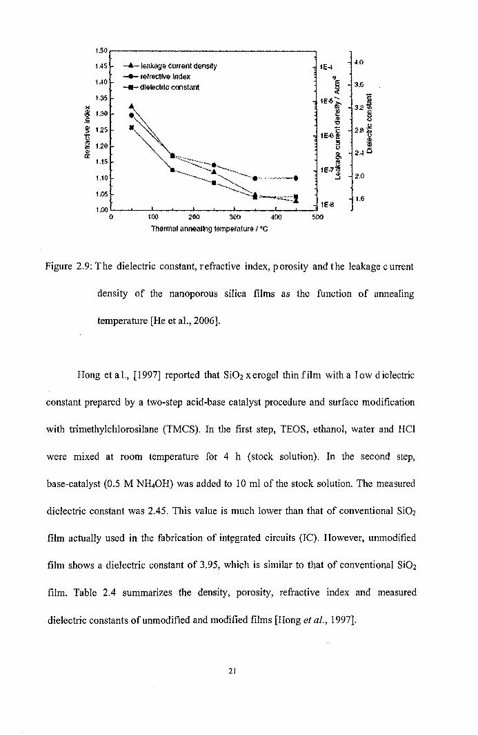
1.50
1.45 .....-Ieakage cunent density 1E44.0
1.40...- refrectlve Index '1
___ dlelec,rlc coostan, ~ 3.6
1.35 fEoo ....3.2 ix .. ~
~ 1.30
:\"~ §.s; 4>"0
~ 1.25 ~ 1E.{)i 2.8 i-<.lll:l 1.20 :s ifi.:::. l)
2.4 0~ ~1.15 ~- ....... ll:l
'.,'~. fE.7a~-. -.~L10 ~,.....__~ ·'e,,·· ._-. ~ 2.0
1.05~-.:;.
'--"~""'I 1.6-"",,,,,
1.00lE-a
0 100 200 MO 400 500
Thermal annealing temparatur& ! 9C
Figure 2.9: T he dielectric constant, refractive index, porosity and t he leakage current
density of the nanoporous silica films as the function of annealing
temperature [He et aI., 2006].
Hong et aI., [1997] reported that SiOz x erogel thin film with a low dielectric
constant prepared by a two-step acid-base catalyst procedure and surface modification
with trimethylchlorosilane (TMCS). In the first step, TEOS, ethanol, water and HCl
were mixed at room temperature for 4 h (stock solution). In the second step,
base-catalyst (0.5 M NIttOH) was added to 10 ml of the stock solution. The measured
dielectric constant was 2.45. This value is much lower than that of conventional SiOz
film actually used in the fabrication of int~grated circuits (Ie). However, unmodified
film shows a dielectric constant of 3.95, which is similar to that of conventional SiOz
film. Table 2.4 summarizes the density, porosity, refractive index and measured
dielectric constants of unmodified and modified films [Hong et al., 1997].
21

Table 2.4: Characteristic data of Si02 xerogel [Hong et ai., 1997].
Ellipsometer Modified film Unmodified film
Density (g/cm3) 1.29 1.93
Refractive index 1.26 1.39
Porosity (%) 43.2 15
Dielectric constant 2.45 3.95
2.2.5 Requirements of Low Dielectric Constant Materials
There are few general requirements for a low k material to be successfully integrated.
They are [Shamiryan et ai., 2004]:
i) Hydrophobicity
ii) Mechanical stability
iii) Thermal stability
iv) Chemical and physical stability
v) Compatibility with other materials
vi) Reliability
2.3 Interlayer Dielectric (ILD)
2.3.1 Introduction of Interlayer Dielectric
A fully processed four layer multilevel metallization (MLM) interconnect cross
22

section is shown in Fig. 2.1 O. In Fig. 2.1 0 there are five layers of dielectric shown for
the four layer metal structure. The first four are referred to as interIayer dielectric layers
(ILDs) and serve to insulate the metal layers within the layer and from each other. The
ILD separating the silicon from the first metal interconnect layer is referred to as ILD O.
The ILD separating the first layer of metal from the second is referred to as ILD 1. ILD
2 and ILD 3 then, are the dielectric layers between metal 2 and metal 3, and metal 3 and
metal 4, respectively.
The final layer of dielectric is referred to as the passivating layer. The purpose of
this layer i s to provide physical a nd chemical protection tot he underlying metal and
device structure during the final assembly processes. Generally, this layer is composed
of one or more layers of dielectric whose composition may act as mobile ion barriers or
inhibit the diffusion of moisture and corrosive ions to metal surfaces [Wilson et aI,
1993].
Figure 2. I0: Schematic cross section ofa four layer metal system [Wilson et aI, 1993].
23

2.3.2 Deposition of Interlayer Dielectric
2.3.2.1 Sol-Gel Deposition Technique
The sol-gel process is a versatile solution process for making thin films. In
general, the sol-gel process involves the transition of a system from a liquid "sol"
(mostly colloidal) into a solid "gel" phase. Applying the sol-gel process, it is possible
to fabricate materials in a wide variety of forms: ultra-fine or spherical shaped powders,
thin film coatings, ceramic fibers, microporous inorganic membranes, monolithic
ceramics and glasses, or extremely porous aerogel materials. The sol-gel process can be
described by the hydrolysis and condensation reactions of the precursors [Yu et ai.,
2004]:
Hydrolysis:
Si - OR + H20 ~ Si - OH + ROH
Water condensation:
Si - OH + HO - Si ~ Si - 0 - Si + H20
Alcohol condensation:
Si - OR + HO - Si ~ Si - 0 - Si + ROH
(2.5)
(2.6)
(2.7)
The alkoxide groups (OR) are replaced by hydroxyl groups (OH) in the
hydrolysis reaction. The sHanol groups are subsequently involved in the condensation
reactions producing siloxane bonds (Si-O-Si). In practice, it is impossible that all the
Si-OH bonds are transformed to Si-O-Si bonds. However, the remaining hydroxyl 0 r
24
silanol groups in the final product are harmful to dielectrics because they are readily
absorbing moisture from the atmosphere. The absorbed moisture may increase the
dielectric constant of the silica films and cause via hole poisoning and other integration
problems.
Thus, surface modification is necessary to reduce the silanol groups and keep the
dielectric constant of the films low. The surface hydroxyls can be removed by thermal
or chemical treatment of the samples. The sequence of surface dehydration is the initial
removal of physically adsorbed water at low temperatures followed by the progressive
removal of weakly hydrogen bonded hydroxyls, strongly hydrogen bonded hydroxyls
and finally isolated hydroxyls [Yu et ai., 2004].
2.3.2.1.1 Type of Precursor
There are many different types of precursor that can be used. All should be
soluble inorganic solvents and easily converted to the relevant oxide preferably by
hydrolysis but alternatively by chemical reaction or oxidation decomposition. Several
preparative methods are available dependant on the nature of the starting materials.
There are different types precursor can be using as long as it will soluble like:
1. Salt
11. Hydroxide
111. Oxide
IV. Alkoxide
25

Probably the best starting materials for sol gel preparation are the class of
materials known as alkoxides. All form alkoxides have the following general formula
[Lisa,1988J:
M(OR)x
where M =silicon
R = alkyl group
x =valence state of the silicon
(2.8)
For long-term applications, the sol-gel thin films need to have water repellent
like hydrophobic property. Several co-precursors can be used for this purpose. Even
though there a re some reports on the tetramethoxysilane (TMOS) based hydrophobic
aerogels but the TMOS is highly toxic and it is very expensive. Therefore, in the present
studies TEOS precursor have been used to make hydrophobic silica thin film because
TEOS is non-toxic a nd the cost is at least four times lower compared tot he TMOS
precursor [Rao & Kalesh, 2003].
2.3.2.1.2 Effect of Water: Alkoxide Ratio (R)
The ratio of water: alkoxide (R) determines the amount of co-solvent required,
but this ratio also influences the reaction rate. Fig. 2.11 showed the phase diagram for
26

TEOS / Ethanol/Water [Brinker & Scherer, 1990].
TEOS
ALCOHOL
Immiscible
WATER
Figure 2.11: The phase diagram for TEOS / Ethanol/Water [Brinker & Scherer, 1990].
If the amount of water becomes very small, however, the hydrolysis rate slows
down due to the reduced reactant concentration. Similarly, if very large amounts of
water are used the other reactant (alkoxide) is effectively diluted [Brinker & Scherer,
1990].
Figure 2.12 plots the dependence of film thickness upon the volume percent of
TEOS in the solution. The lines in the upper right with the open points represent films
prepared with the H20 / TEOS ratio equal to four. The TEOS content of each solution
was varied here by increasing the H20 / TEOS ratio. Thus, the dotted line extrapolation
would represent the situation where the additional water simply dilutes the oxides
present in the solution and the water influences the condensation of the oxide film
27

[Glaster & Pantano, 1984].
I I I14 15 16
Figure 2.12: The dependence of film thickness upon the volume percentage of TEOS
in ternary solutions ofTEOS + H20 + C2HsOH [Glaster & Pantano,
1984].
2.3.2.1.3 Sol-gel Spin On Coating
Spin coating has been used for several decades for the application of thin films.
A typical process involves depositing a few drop of precursor onto the center of a
substrate and then spinning the substrate at high speed (typically around 3000 rpm).
Final film thickness and other properties will depend on the nature of the precursor
(viscosity, drying rate, percent solids, surface tension, etc.) and the parameters chosen
for the spin process. One of the most important factors in spin coating is repeatability.
For sure repeat the spinning processes will thicker the layer (Klein, 1991). Fig. 2.13
28
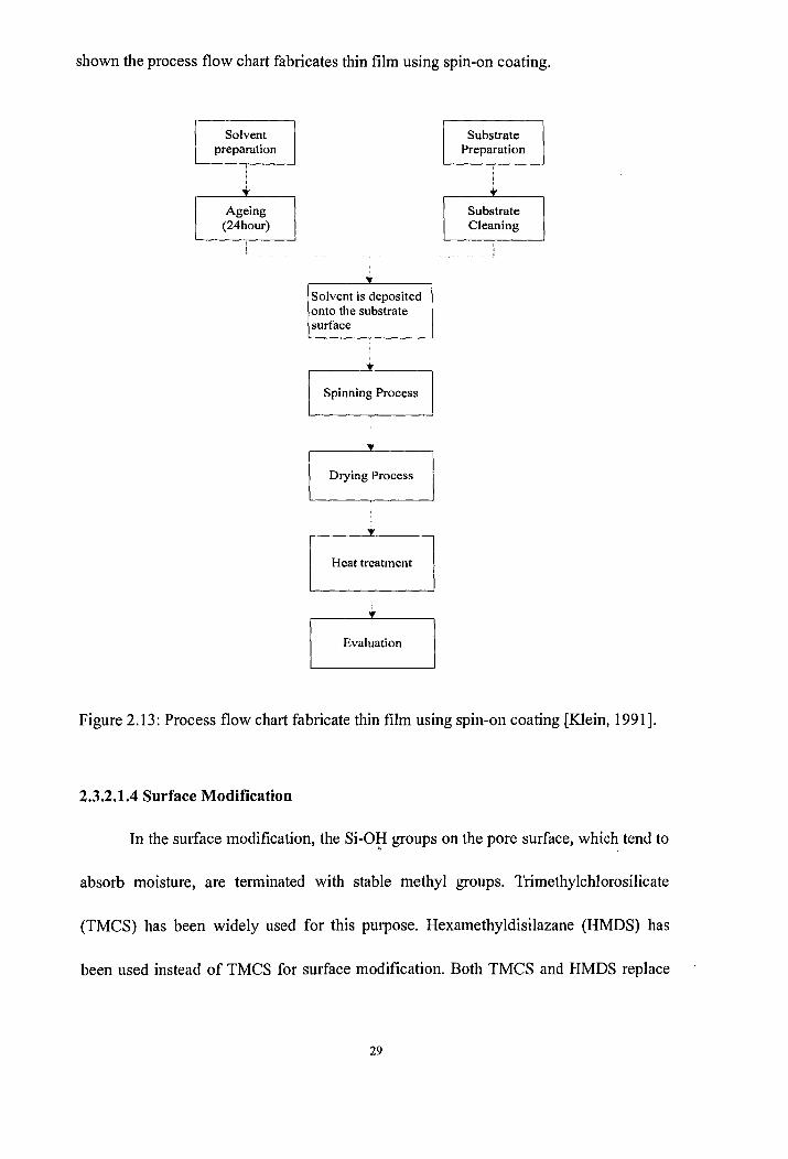
shown the process flow chart fabricates thin film using spin-on coating.
Solventpreparation
i...Ageing
(24hour)
Solvent is depositedonto the substratesurface
Spinning Process
..Drying Process
Heat treatment
..Evaluation
SubstratePreparation
SubstrateCleaning
Figure 2.13: Process flow chart fabricate thin film using spin-on coating [Klein, 1991].
2.3.2.1.4 Surface Modification
In the surface modification, the Si-OH groups on the pore surface, which tend to, .
absorb moisture, are terminated with stable methyl groups. Trimethylchlorosilicate
(TMCS) has been widely used for this purpose. Hexamethyldisilazane (HMDS) has
been used instead of TMCS for surface modification. Both TMCS and HMDS replace
29

the higher polar hydroxyl groups on the surface of the film with less polar methyl
groups [Manjari et ai., 2002].
However, TMCS contains chloride and hydrochloride acid (HCI) generated
during processing may corrode the metal lines. This is serious concern for xerogel films
to be used as interlayer dielectric in very large scale integrated technology. On the other
hand, HMDS does not contain any chlorine and is therefore better suited for this
application [Manjari et ai., 2002J.
The dielectric constant of the films underwent different surface modification is
compared in Fig. 2.14. The dielectric constant reduced from 4.33 for no HMDS treated
film to 3.07 for HMDS-treated film and further reduced to the ultralow k region of 1.89
for HMDS and air plus nitrogen dehydroxylated film. Therefore, the HMDS chemical
modification and air plus nitrogen two-step annealing are very effective in
dehydroxylation and lowering the dielectric constant of the silica films [Yu et ai.,
2004J.
30

4.5
4.01:III1ii 3.5c:o(Ju 3.0
.£:....u
.!!!. 2,5
.!!!C
2.0
HMOS soakair anneal
HMDS soak +'.(air T Nt) anneal
1.5....1...------------------'Various Dehydroxylation
Figure 2.14: Dielectric constant of the films with different surface modifications
[Yu et al., 2004].
2.3.2.1.5 Annealing Process
Annealing is a heating process in which a wafer is heated to achieve a desired
physical or chemical change with minimum material being added to or removed from
the wafer surface [Hong, 2001]. Yu et aI., [2004] report that the porosity of the films
will increased with temperature. The refractive index, porosity and dielectric constant of
the films annealed at different temperatures are tabulated in Table 2.5. The porosity of
300 ° C film was found to be much lower and the dielectric constant 0 f it was much
higher than that of other two samples; whereas the properties of both 400°C and 450 °c
samples were more close. The changes of porosity and dielectric constant of the 400°C
and 450 °c film with respect to 300°C film are shown in Fig. 2.15 (Yu et al., 2004).
31

Table 2.5: Effect of thermal treated temperature on the properties of the films [Yu et ai.,
2004].
Temperature (OC) 300 400 450
Refractive index 1.31 1.22 1.18
Porosity (%) 24.3 47.01 56.96
Dielectric constant 3.12 2.3 2.11
160
140
- 120~..- 100lIJQ)
E 80Q)c..0 60..Q.
'0 40lIJ 20Q)tnC 0co.cU -20
-40
+134.4%
Dielectric Constant
Figure 2.15: The changes of dielectric constant and porosity of the films with respect to
the 300°C film [Yu et ai., 2004].
,The porosity increased about 93.46 % and 134.4 % and the dielectric constant
decreased by 26.28 % and 32.37 % for 400°C and 450 °c films, respectively, compared
to that of 300°C film. The higher porosity with increasing temperature results in lower
dielectric constant of the films [Yu et ai., 2004]
32

2.3.2.1.6 Advantages of Sol-Gel Technique
There are several advantages of sol-gel processed oxides over thermal oxides
[Weimer et at., 1987]:
1) The composition and microstructure of the oxide may be precisely tailored imd are
independent of the composition of the substrate.
2) Sol-gel films may be deposited at room temperature on any substrate.
3) Film thickness can controlled by the deposition process
4) Multilayer films, consisting, e.g., of alternating layers of two different compositions,
are easily to obtained by multiple spinning
2.4 Morphology Characterization of Film Layer
2.4.1 Film thickness
Oxide thickness will be an important parameter in process characterization and
have many technique can use to measure the thickness. Perhaps the simplest method for
determining the thickness of an oxide is to compare the color of the wafer with a
reference color chart. Apart from that, thickness thin film also can be measure using thin
film measurement system 1ike filmetrics, elipsometrics, profilometer and etc [May &
Sze,2002].
2.4.2 Refractive Index
The definition of refractive index is:
33

Refractive index, n =Speed of light in a vacuum / Speed of light in the film (2.9)
For Si02, refractive index = 1.46. The refractive index is related to the
wavelength of the light used for the measurement. A prism separates white light into a
colorful light spectrum; this is because the refractive index of this prism material, quartz,
is a function wavelength of the light. Light with different wavelengths has different
refractive angles inward to and outward from the prism, giving the colorful spectrum of
light [Hong, 2001].
The refractive index and refractive angle illustrated in Fig. 2.16 can be described by the
equation of refraction:
(2.10)
Here nl is the refractive index of the first dielectric material, usually air with a
dielectric index very close to 1. The incident angle is 81, n2 is the refractive index of the
second dielectric material, and 82 is the refractive angle. This equation can be used to
measure the dielectric index by shining a laser beam into the dielectric material and
measuring the refractive angle. However, it is impossible to measure the refractive
index of a dielectric film by applying this equation when film thickness is too thin,
[Hong, 2001].
34

Incident light
Vacuum
. Films·•. 2.
Figure 2.16: Refractive index and refractive angle [Hong, 2001].
For the silicon compound dielectric thin film, the refractive index measurement
can give some useful information on the film's chemical composition and the physical
conditions of the film. For the silicon- or nitrogen- rich oxide, the refractive index will
be higher than the stoichiometric value of 1.46, but it will be lower than that value when
it is oxygen rich [Hong, 2001].
The dependence refractive index of the silica films on annealing temperature are
presented in Fig. 2.17. It is observed that the refractive index of the film annealed at 50
°c is 1.297. As the annealing temperature increases to 150°C the refractive index
decreases accordingly, which is from the evaporation of the physisorbed water. Because
of the pyrolytic of organic ingredients in films,' the refractive index goes on decreasing
continuously and reached the lowest value of 1.101 at 350°C [He et al., 2006].
35

150
1.45
1.40-e- refractiVe Index
1.35)(
~ 1.30
.~.f;
~ 125..,.(.)
~ 1.20(1) ''ea:
1.15 -..........._-.'-"
1.10-"--'"....... •
1.05
1.000 100 200 300 400 500
Thermal annealing temperature / °C
Figure 2.17: The refractive index of the nanoporous silica films as the function of
annealing temperature [He et al., 2006].
2.4.3 Qualitative and Quantitative Chemical Species Determination
Qualitative and quantitative chemical species determination at certain sample
can be done using Fourier Transform Infrared Spectroscopy (FTIR). FTIR is most
useful for identifying chemicals that are either organic or inorganic. It can be utilized to
quantitative some components of an unknown mixture. It can be applied to the analysis
of solids, liquids, and gasses. The term Fourier Transform Infrared Spectroscopy (FTIR)
•refers to a fairly recent development in the manner in which the data is coIIected and
converted from an interference pattern to a spectrum. Today's FTIR instruments are
computerized which makes them faster and more sensitive than the older dispersive
instruments [Runyan & Shaffner, 1997].
36

The F TIR spectra 0 f films h eat-treated at different temperatures are shown in
Fig. 2.18. The most intense absorption peak located at 1060 cm- ] is the transverse
optical (TO) vibration ofSi-O-Si linkage. The peak centered around 1100 cm-) as a
shoulder at the high frequency end of 1060 em-I peak assigns to the corresponding
longitudinal optical (LO) vibration of Si-O-Si linkage. Yu et at, [2004] explained the
appearance of the LO shoulder as scattering due to the porous nature of the samples.
The peak located in 775 cm-] is associated with symmetric stretching of Si-O-Si
linkage.
1.6
1.4 O-H
as deposited
0,2
4000 3600 3200 2800 2400 2000 1600 1200 800001
Wavenumber (em)
Figure 2.18: FTIR spectra of films annealed at different temperature [Yu et al., 2004].
The broad peak between 3300 cm-) and 3700 cm-) corresponds to a stretching of
-OR and physisorbed moisture on the surface in several modes. There was a very great
-OR peak for the as-deposited film indicating the high content of the silanol groups.
37

With increasing temperature, the peak intensity around 3300 cm-I_ 3700 cm-1 decreased
gradually, so more silanol groups were removed at higher temperature. Furthennore, the
peak area around 1100 cm- I was also increased with increasing annealing temperature,
suggesting the porosity of the films increased [Yu et al., 2004].
2.4.4 X-Ray Diffraction (XRD)
X-ray diffraction is a nondestructive technique for detennining structural crystal
defeats. It requires little sample preparation and gives structural information over entire
semiconductor wafers. The XRD image is not magnified because no lenses are used.
XRD give microscopic information through photographic enlargement of the topograph.
Consider a perfect crystal arranged to diffract monochromatic X-rays of
wavelength Afrom lattice planes spaced d. The X-rays are incident on the sample at an
angle a, as shown in Fig. 2.1 9.
Reflecling. Crystal Planes
Figure 2.19: Berg-Barrett reflection topography.
38

The primary beam is absorbed by or transmitted through sample; only the
diffracted beam is recorded on the film. The diffracted beam emerges at twice the Bragg
angle Sa defined by
Ela =sin-I (JJ2d) (2.11)
The diffracted X-ray are detected on a high-resolution, fine grained
photographic plate or film held as close as possible to the sample without intercepting
the incident beam.
2.4.5 Atomic Force Microscope (AFM)
Atomic force microscopy (AFM) operates by measuring the forces between a
probe and the sample. These forces depend on the nature of the sample, the distance
between the probe and the sample, the probe geometry, and sample surface
contamination. AFM is suitable for conducting as well as insulating samples. The AFM
principle is illustrated in Fig. 2.20.
47-~ Piezoelectricx Y Tube Scanner
Figure 2.20: Schematic Illustration of an atomic force microscope.
39

2.4.6 Scanning Electron Microscope (SEM)
The scanning electron microscope (SEM) is a microscope that uses electrons
rather than light to form an image. There are many advantages to using the SEM instead
of a light microscope. The SEM has a large depth of field, which allows a large amount
of the sample to be in focus at one time. The SEM also produces images of high
resolution, which means that closely spaced features can be examined at a high
magnification. Preparation of the samples is relatively easy since most SEM only
require the sample to be conductive. The combination of higher magnification, larger
depth of focus, greater resolution, and ease of sample observation makes the SEM one
of the most heavily used instruments in research areas today.
Figure 2.21 shown the microstructure of the silica aerogels was observed using
scanning electron microscope (SEM). The silica aerogels was prepared using TEOS as
precursor and MTES as co-precursor. Image of SEM indicate that the MTES modified
aerogels have uniform particle and pore sizes [Rao & Kalesh, 2004].
Figure 2.21: S EM microstructure of silica aerogels modified using the molar ratio 0 f
MTES / TEOS = 0.3 [Rao & Kalesh, 2004].
40

2.4.7 Electrical Properties
An electrical current flowing through a solid, and having units of charge per unit
time per unit area (measured in the direction perpendicular to the flow direction). For
electrons with number density, ne flowing through a solid with velocity, v the
resulting volume current J is given by:
J =-enev (2.12)
where - e is the charge on an electron. Experimentally, it is observed that the volume
current is proportional to the applied electric field E,
where a is conductivity
J=aE (2.13)
Yu et aI., [2004] report that the leakage current of the silica films at 1 MY / cm
was reduced with increasing temperature as shown a t Fig. 2.22. T he leakage current
density at 1 MV / cm for the 300°C film was as high as 8.4xlO-3 A / cm2, it reduced to
8.1xI0-6 A / cm2 for 400°C film and 1.6xl0-7 A / cm2 for 450°C film, respectively.
41

0.01
300"C1E-3
.a-'j;)
1Ew1cQl
Q 400"CC ....E 1[:-5~....ud $. 1E-6
4503 CQlat~ 1E-7I'llQl
...I 1E-8
1,00.2 0.4 0.6 0.8Applied Field (MV/cm)
1E-9 -t--....---r--.--,----.---,.--..----r--.....--!0.0
Figure 2.22: I-V property of different temperature treated films [Yu et al., 2004].
42

CHAPTER 3: METHODOLOGY
3.1 Introduction
Fabrication SiOz thin film with silicon wafer as substrate was studied in this
research. Silicon wafer use is n-type and (100) plane. The wafer cut to small piece using
diamond cutter, the small piece is use as sample. To remove the organic and inorganic
contamination from silicon wafers, procedure RCA (Radio Corporation of America)
cleaning was introduced. The SiOz layer had been deposited at Si wafer using spin-on
coating technique. The precursors used are (1) inorganic tetraethyl orthosilicate (TEOS)
and (2) mixture of TEOS and organic methyItriethoxysiIane (MTES). The incorporation
of organic precursor makes it easier to get crack-free films with thickness 100 nm. The
ratio of TEOS and MTES also has a great influence on the structural and dielectric
properties of the films. Various surface modifications have been conducted to remove
the silanol groups and their effects on film properties have been studied by advanced
techniques.
3.2 Experimental Design
The experimental work was designed properly to fulfill the research objectives.
The fabrication and characterization of the silicon dioxide sol-gel thin film was carried,
out in 2 phases. Phase I is about the sol-gel thin film fabrication and phase 2 is
characterization process. There are as shown in Fig. 3.1 and Fig. 3.2.
43

Wafer Preparation
...
Wafer Cleaning
..Sol-Gel preparation
..Spin Coating of the sol
gel thin film
Surface ModificationOnly for film derived
from TEOS/MTES
Annealing Process
PhysicalCharacterization
Characterization
I ... ~~ .• • Metallization Processes
Photolithography
Process
ElectricalCharacterization
Figure 3.1: Flow chart of the fabrication process - phase 1 of the experiment.
44

Thickness & Refractive
Index Measurement
FTIR Measurement
..Characterize Electric
Properties
X-Ray Diffraction(XRD)
Atomic ForceMicroscope (AFM)
Figure 3.2: Flow chart of the characterization process - phase 2 of the experiment.
45

3.3 Phase 1: Fabrication Process
3.3.1 Wafer Preparation
N-type silicon wafer with diameter 2 inch and orientation (100) was used to prepare the
sample. Generally wafer silicon using in this research have characteristic as below:
~ Diameter : 2 Inch
~ Type and dopant : N-Phosphorus
~ Resistivity : 0.75-1.25 Ocm
~ Thickness : 275 ± 25 11m
~ Processing method : Czochralski (Cl)
~ Orientation : (I 00)
The wafer is cut to dimension 1 cm x 1 cm using diamond cutter. Wafer cutting step is
as below:
Place the wafer on a cutting board. Do not touch the Si wafer with your hands.
Use tweezers to handle wafer.
Place diamond cutter on the very edge of the Si wafer and press down firmly.
The Si wafer should cleave easily.
3.3.2 Wafer Cleaning
Contaminants present on the surface of silicon wafers at the start of processing,
or accumulated during processing, have to be removed at specific processing steps in
order to obtain high performance and high reliability semiconductor devices. The RCA
46

clean is the industry standard for removing contaminants from wafers. Werner Kern
developed the basic procedure in 1965 while working for RCA (Radio Corporation of
America). Chemicals use for the RCA cleaning and their Physical and Chemical
Properties are shown in Table 3.1. The standard RCA cleaning procedure has five major
steps used sequentially:
1. Remove greasy impurities which may be residue from the photoresist.
2. Remove metallic contamination.
3. NH40H: Hz02: H20 = 1:1:5, 70-80°C for 10 min: Remove organic firms,
desorption of trace metals.
4. Dissolve alkali ions and hydroxides of Al+3, Fe+3
, Mg+2•
5. Remove oxide and trace metals in oxide.
3.3.2.1 Chemical Reagents
1. Hydrogen Peroxide
2. Sulfuric acid
3. Ammonium Hydroxide
4. Hydrochloride Acid
5. Hydro fluoride Acid
6. Deionized water
47

Table 3.1: Chemicals use for the RCA cleaning and their physical and chemical
properties.
Raw Hydrogen Sulfuric Ammonium Hydrochloride Acid Hydro
material Peroxide Acid Hydroxide Fluoride Acid
Chemical H202 H2SO4 NH40H HCl HF
Formula
Molecular 34.01 98.08 35.05 36.46 20.01
Weight (g
/ mol)
Melting -25 3 -72 -74 <-36
Point (0C)
Boiling 108 280 36 85 108
Point (0C)
Density 1.17 1.84 0.9 1.1-1.2 1.97
(g / ml)
Physical Clear, Colorless Clear, Colorless, fuming Colorless,
Property colorless to brown colorless liquid fuming liquid
liquid liquid solution
Chemical Slight Odorless Ammonia Pungent odor of Acrid odor,
Property acrid odor hydrogen chloride do not breathe
odor fumes
Solubility Infinitely Miscible in Infinitely Infinite in water with Infinitely
soluble all soluble slight evolution of soluble,proportions heat
48
3.3.2.2 Apparatus
1. Glass beaker 500 ml x 2
2. Fused silica beaker 250 ml x 2
3. Plastic beaker 250 ml x 2
4. Thermometer
5. Hot Plate
6. Retort & Clamp
7. Dryer
8. Volumetric cylinder 10 ml & 50 ml
3.3.2.3 Experimental procedure:
a) Remove greasy impurities
1. Fresh mixture of H2S04 : H202 (4:1) is prepared by measuring the following reagents
into fused silica beaker.
2. Wafer are submerged in cold solution and the beaker is placed on hot plate and heat
to 90°C.
3. The solution is maintained at 90 °c for additional 10 min.•
4. Wafers are removed from the beaker and rinsed immediately with DI water for more
than 5 min.
5. The wafer is rinsed in ultrasonic bath for 3 min.
49

b) Remove metallic contamination
1. Wafers are submerged directly in a mixture of HF : H20. The solution is prepared
by mixing 40 ml of Dr water and 10 ml HF in a plastic beaker.
2. Wafers are allowed to remain in the solution for 1 min.
3. After that, the wafers are rinsed with DI water for 5 min or more to remove the HF
solution.
4. The wafers are rinsed in ultrasonic bath for 3 min.
c) Remove organic firms, desorption oftrace metals.
1. Fresh mixture of NH40H-Hz02-HZO (0.5 :1 : 4) is prepared by measuring the
following chemical reagent into a fused silica beaker.
a) 7 ml ofNH40H
b) 14 ml of HzOz
c) 50 ml ofHzO
2. The beaker is placed on the hot plate and heated up to 70°C.
3. Still wet wafers are submerged in the hot solution.
4. The solution is maintained at 70 °c for 10 min.
5. The wafers are rinsed with DI water for more than 5 min.
6. The wafers are rinsed in ultrasonic bath for 3 min.
d) Dissolve alkali ions and hydroxides
1. Fresh mixture of HCI-HzOz-HzO (1 : 1 : 4) is prepared by measuring the following
chemical reagent into a fused silica beaker.
50

a) 10 m1 ofHC1
b) 10 ml ofH20 2
c) 40 ml of H20
2. The beaker is placed on the hot plate and heated up to 70°C.
3. Still wet wafers are submerged in the hot solution.
4. The solution is maintained at 70 °c for 10 mins.
5. The wafers are rinsed with DI water for more than 5 min.
6. The wafers are rinsed in ultrasonic bath for 3 min.
e) Remove oxide and trace metals in oxide.
1. Wafers are submerged directly in a mixture of HF : H20. The solution is prepared
by mixing 2 ml ofDI water and 98 ml HF in a plastic beaker.
2. Wafers are allowed to remain in the solution for only lOs.
3. After that, the wafers are rinsed with DI water for only 20-30 s to remove the HF
solution.
4. The wafers are rinsed in ultrasonic bath for 3 min.
3.3.3 Sol-Gel preparation
3.3.3.1 Chemical Reagent
1. Tetraethyl Orthosilane (TEaS)
2. Methyltriethoxysilane (MTES)
3. Hydrochloride Acid (HCI)
51

4. Ammonium Hydroxide (NH40H)
5. Ethanol
6. DI Water
3.3.3.2 Experimental procedure:
Experimental Procedure for TEOS derived Si02 film:
Tetraethyl orthosilicate (TEOS), deionized water (DI), ethanol, and HCl were used to
prepare a crystal clear precursor for the sol-gel derived Si02 thin films. Firstly, a
mixture of 12.4 mole ratio of DI:TEOS was prepared under stirring condition. An
appropriate amount of ethanol was added to the mixture and then followed by a few
drops of HCl to control pH of the precursor. The precursor was stirred for 90 min so
that hydrolysis could be initiated. The product was then divided into four equal amounts
and stored in four different beakers. The beakers were labeled as A, B, C, and D;
indicating the aging time for the precursor before deposition. The aging time for A, B,
C, and D were 0, 2, 4, and 6 days, respectively. After underwent an appropriate aging,
the precursor was ready to be applied on a RCA-cleaned Si (100) wafer. A spinner was
used to perform the spin-on-coating process with a speed and time of 4000 rpm and 45
s, respectively. After spinning, the sample was inserted in a chamber with UV
wavelength of 250 nm for the post deposition treatment. The samples were exposed at
the same wavelength for different durations. After the treatment the samples were sent
for characterization.
52

Experimental Procedure for TEOS/MTES derived Si02 film:
1. The solution used to prepare the SiOz sol-gel thin film consisted of two types of
sols.
2. Sol A consisted of tetraethorthosilane (TEOS), ethanol, and deionized water.
Volume of solution A in 100 ml total solution shown in Table 3.2.
3. Sol B consisted of methyltriethoxysilane (MTES), ethanol, and deionized water.
Volume of solution Bin 100 ml total solution shown in Table 3.3.
4. A small amount of 1 M HeI acid was added to sol A and a small amount of 1 M
NH40H was added to sol B.
5. Both sols were allowed to hydrolyze for about 24 hour before mixing them together
with different ratios of s 01 A and sol B. Ratio 0 f solution A and solution Bare
shown in Table 3.4..
6. Mix sol A and B according to the different ratios (l : 1, 2 : I, 4 : 1, 6 : I).
7. The solution is ready for spin coating immediately.
Table 3.2: Volume of solution A in 100 ml total solution.
Moles Ratio H20 I TEOS H20lml TEOS Iml Ethanol I ml
12 33 33.5 33.5
53

Table 3.3: Volume of solution Bin 100 ml total solution.
Moles Ratio H20 I MTES H20 / ml MTESlml Ethanollml
12 33 33.5 33.5
Table 3.4: Ratio of solution A and solution B used to prepare sol-gel solution.
Ratio 1: 1 2:1 4:1 6:1
Solution A (ml) 4 8 12 24
Solution B (ml) 4 4 4 4
3.3.4 Spin Coating of the sol-gel thin film
Spin Coating Process Description
1. Start up the spin coater and flow the Argon gas into the spin coater for few second.
2. The rotational speed and dwell time were set. Speed of rotation for the spin coater
was set to 3000 rpm and dwell time was set to 15 s.
3. Switch on the vacuum and ensure that the vacuum is function. Vacuum is important
in holding the substrate to avoid the substrate flyaway when the spinning process.
4. The cleaned Si substrate was placed on the middle of the stage. The stage is
connected to the vacuum pump hence it can hold the Si substrate.
5. The precursor was dropped on the substrate by using a dropper.
6. Start the spin coater by press the start button. The silica gel will spread uniformly
on the substrate surface.
7. After the spin coater stop spinning and the "safe to remove coated part" appear on
54

the screen only the sample was removed from the spin coater.
8. The coated substrate need to be annealed immediately after spin coating to avoid
further oxidation and contamination of the sample. If unavoidable, the coated
sample need kept in the desiccators.
9. The processing step is repeated for different substrate. Flows chart of Spin Coating
Process are shown in Fig. 3.3 and spin-on coating machine are shown in Fig.3.4.
Start up the spin coater
Flow the Argon gas
Set the rotational speed and dwelltime
Switch on the vacuum to holdingthe Si substrate
The cleaned Si substrate was placedon the middle of the stage
Dropped the precursor on thesubstrate
Start the spin coating
Removed sample from the spincoater safely.
The coated substrate need to beannealed immediately
Figure 3.3: Process flow of Spin Coating Process.
55
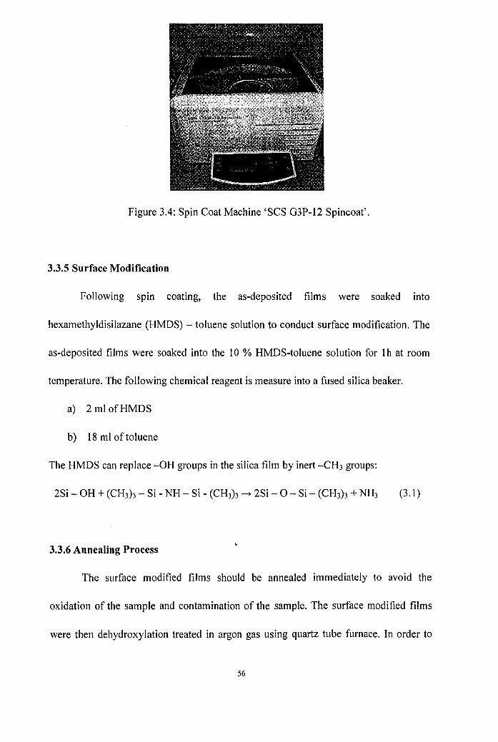
Figure 3.4: Spin Coat Machine 'SCS G3P-12 Spincoat'.
3.3.5 Surface Modification
Following spin coating, the as-deposited films were soaked into
hexamethyldisilazane (HMDS) - toluene solution to conduct surface modification. The
as-deposited films were soaked into the 10 % HMDS-toluene solution for 1h at room
temperature. The following chemical reagent is measure into a fused silica beaker.
a) 2 ml ofHMDS
b) 18 ml of toluene
The HMDS can replace -oH groups in the silica film by inert -CH3 groups:
2Si - OH + (CH3)3 - Si - NH - Si - (CH3)3 -+ 2Si - 0 - Si - (CH3h + NH3 (3.1)
3.3.6 Annealing Process
The surface modified films should be annealed immediately to avoid the
oxidation of the sample and contamination of the sample. The surface modified films
were then dehydroxylation treated in argon gas using quartz tube furnace. In order to
56

investigate the effect of processing temperature on the properties of the films, the films
were heat treated at 300 DC, 400 DC, and 500 DC for 30 min. Wait until furnace at set
point temperature. Put the sample fixed on the quartz boat and slide boat slowly and
gently into furnace using quartz rod. Make sure the boat is at middle of the quartz tube
for uniform heating. The samples need to hold at that temperature for 30 min. After
elapsed time, slide sample to edge of tube with quartz rod. Let sample cool for 10 min.
When sample is cool, remove samples from furnace. Turn off heater. It is important that
a small amount of gas flow while furnace is cooling, this is because as the furnace cools,
air inside contracts drawing in air with dust. Over a short time this dust will contaminate
the tube. Fig. 3.5 had shown the temperature profile for annealing.
300 DC
Temperature (DC)
30 min
Time/minutes
Figure 3.5: Temperature profile for annealing of the sample.
3.3.7 Metallization Process
In the metallization process, a layer of metal is deposited on the wafer surface to
provide electrical contact to the devices. Metal can be deposited using several different
methods- sputtering, evaporation or plating. Metallization process in this project is used
57

thermal evaporator system, metal using will be aluminums. The following steps make
up the metallization process:
First remove the outside cover from the evaporator. Then remove the wafer
holder. This is where the wafers will be during the evaporation process. The metal will
be placed in a tungsten boat (tungsten has a relatively high melting p oint). Carefully
load the wafers into the wafer holder. Place the cover back onto the evaporator. Installed
tungsten boat between the two electrodes. When the chamber has been pumped down
sufficiently, current is applied through the boat or filament to heat the aluminum inside
to melt, the molecule which will travel in a line-of-sight path to the sample. Allow
wafers to cool down for 15 min, and then remove the wafer holder. Use tweezers to
remover the wafers. Structure semiconductors after metallization are shown in Fig. 3.6.
Aluminium
Silicon
Figure 3.6: Schematic Illustration layer structure semiconductor after metallization.
This processes need to be done at high vacuum environment to secure fr9m dirty
particle or air particle that will effected the aluminum depositions at surface wafer.
Always make sure the sample is clean to ensure there are no dirty particles in interlayer
58

structure capacitor. Dirty particle will affect the properties electricity capacitor.
3.3.8 Photolithography Process
Photolithography is a process analogous to developing film in a darkroom. The
purpose of photolithography is to transfer images from a mask to the surface of photo
resist layer on a wafer. Photo resist is a film used in photolithography that temporarily
holds the pattern of a circuit path or microscopic element of a chip. The process flows
for photolithography are shown at Fig. 3.7.
Metallization Process
PhotoresistApplication
jt
Soft Bake
Exp~sure
Development
Hard Bake,t
Etching
Pattern TransferComplete
Figure 3.7: Process flow of Photolithography Process.
59

Using tweezers, place the wafer on the wafer chuck in the center of the photo
resist spinner. After making sure the wafer is centered 0 n the wafer chuck, press the
button to lock on the vacuum line. The vacuum will secure the wafer to the chuck.
Using an eye dropper, flood the wafer surface with primer. Wait ten seconds, letting the
primer dwell on the wafer surface so that it will allow good adhesion between the
photoresist and the wafer surface. Then, start spinning the wafer at 2700 rpm for lOs. In
a manner similar to applying the primer, an eye dropper is also used to place photoresist
on the wafer. Apply the resist so that the whole wafer surface is covered. Spin the wafer
at 2700 rpm for lOs. Then, release the vacuum, and use tweezers to carefully remove
the wafer. Pre-heat the Soft-Bake Oven to the temperature between 80-100 DC. Place the
tin plate containing the wafer into the Soft-Bake Oven for 10 min. The purpose of the
soft bake is to semi-harden the photoresist. The wafer is aligned with respect to the
mask in an optical lithographic system, and the resist is exposed to UV light for 30-35 s.
Exposure can affect the way that the resist image is finally produced and it is important
that the exposure is kept within certain limits. Mask pattern and window area are shown
in Fig. 3.8.
60

• • • Window area9.9856 x 10-4
• • • •• • • •• • • •• • • •Figure 3.8: Schematic Illustration mask pattern.
The exposed areas are subsequently removed in the development process; the
resist image will be identical to the opaque image on the mask. This is identifying as
positive resist as shown in Fig. 3.9.
!
/~("'1=.=::1/
Figure 3.9: Details of the Photolithography pattern transfer process.
61

After the resist exposed to UV light, the exposed resist is dissolved in the
developer. Make sure the development time is suitable and the wafer is then rinsed and
dried. After development, inspect the wafers under a microscope, to see if the patterns
are clear and well defined. If everything looks okay, the wafer is placed into the Hard
Bake oven which should be preheated to between 120-130 °c to increase the adhesion
of the resist to the substrate. After that, the sample is etch using aluminum etchant to
remove the aluminum at area exposed to Uv. Aluminum etchant concentrations are
shown in Table 3.5.
Table 3.5: Aluminum etchant concentrations.
Chemicals Percentage (%)
H3P04 73
RN03 4
CH3COOH 3.5
DI water 19.5
The remaining photoresist is remove using remover. The final s ample is showed I ike
figure 3.1 O.
62

Aluminum
Si02
Substrate
Figure 3.10: Schematic Illustration the final sample after photolithography process.
After that the sample is doing metallization at the sample back side to produce
back contact. Back contacts have been produce using sputtering machine. Before
metallization back contact, the sample back side need to be clean to avoid any oxide
layer using mix solution 1 ml HF and 20 ml Dr water. After that the sample clean with
Dr water to remove the acid solution.
3.4 Phase 2: Characterization
3.4.1 Thickness & Refractive Index Measurement
Perhaps the simplest method for determining the thickness 0 fan oxide is to
compare the color of the wafer with a reference color chart. When an oxide-coated
wafer is illuminated with white light perpe~dicular to the surface, the light penetrates
the oxide and is reflected by the underlying silicon wafer. Constructive interference
leads to enhancement of a certain wavelength ofreflected light, and the color of the
wafer corresponds to the wavelength. Clearly, color chart comparisons are subjective
63

Figure 3.12: Schematic Illustration Fourier Transform Infrared Spectroscopy (FTIR)
machine.
3.4.3 XRD Analysis
The purpose of this analysis is to identify the phase of material. Crystallographic
and phase analysis were perfonned on x-ray diffraction by using monochromatic CuKu
radiation. The detection angle was from 5 to 100 degree and the graph of counts as
angle 28 was recorded. Identification of crystallite phase was carried out by comparison
of XRD patterns with JCPDS standards. In addition to monitoring the evolution of the
microstructure and chemistry, XRD data was carried out to measure the crystallite size.
3.4.4 AFM Analysis
The sample topography is measured <by scanning the tip, which contacts the
surface, across the sample. The tip is brought into continuous contact with the sample
and scanned across the sample surface. When the probe touches the surface, it is pulled
toward the sample by capillary action. By scanning in either way, the local height of the
65

sample is measured. Three dimensional topographical maps of the surface are then
constructed by plotting the local sample height versus horizontal probe tip position.
Conductive - AFM (C-AFM) used to analyze I-V curve. Before analysis the
sample back side needs to clean with HF solution to remove oxide layer during
annealing process. After that, sample need to deposited metal layer at back side to allow
current flow. Machine used for AFM analysis are shown in Fig. 3.13.
Figure 3.13: Schematic Atomic Force Microscope (AFM).
3.4.5 Characterize Electric Properties
Current-voltage measurement was done on the sample which is after
photolithography process. Characterization el((.ctric current-voltage is important because
the chart is to determine basic parameters of a device and to model its behavior in an
electrical circuit.
66

Measurement capacitance-voltage was done using machine measurement model
'KEITHLEY 238 High Current Source Measurement Unit' and software using to
analysis result obtain is Metrics ICS Software. Wafer is place on a plat with 2 terminal,
input and output connect to the wafer and the plat. Output terminal connect at top
surface sample and input terminal connect at opposite side.
67

CHAPTER 4: RESULT AND DISCUSSION
This chapter discussed the results obtained from oxide thickness and refractive
index, Fourier transform infrared spectroscopy (FTIR), X-ray diffraction (XRD), atomic
force microscopy (AFM), scanning electron microscopy (SEM), energy dispersive x-ray
analysis (EDX), and current-voltage (I-V) measurements. Firstly, the results and
discussion on TEOS-derived SiOz films will be presented and then follow by
TEOS/MTES-derived SiOz films.
4.1 TEOS-derived Si02 film
Sample D that has been aged for 6 days has fully transformed into gel form. Therefore it
could not be used in the subsequent process. Figure 4. I shows the result of oxide
thickness as a function of UV exposure time for the three types of samples (A, B, and
C). As UV exposure time increases, the oxide thickness decreases but the changes is
small. This indicates that densification of the gel to solid state occurs as UV exposure
time increases. In contrast, oxide thickness significantly increases as the aging time of
the precursor increases from 0 to 4 days. This is probably due to the increase of
polymerization of the precursor as the aging time increases and attribute to a more
viscous precursor.
68

600Aging
....-,TimeE 550 I-e: -l'-'" I: ! 4 daysx
0 500-CI'JCI'J(1) 450e: !- -1~ I- i 2 days.~
..c: 400I-(1)
"'0'x 3500 ! i j I o day
3001 2 30
UV Exposure Time (h)
Figure 4.1. Oxide thickness as a function of UV exposure time for samples prepared
from precursor aged at different period.
Figure 4.2 presents the refractive index (n) of the thin film as a function of UV
exposure time. All of the samples revealed n value lower than the conventional thermal
and chemical vapor deposited SiOz films (n = 1.46). This indicates that the sol-gel
derived SiOz film in this work probably has a larger porosity or larger chemical
,structures. This may imply that the dielectric constant (k) of the thin film is also
relatively smaller than the SiOz film prepared by conventional methods. As UV
exposure time increases, n value also demonstrated an increasing trend. Contrary, the n
value decreases dramatically as the aging time of the precursor increases. Since the
69

polymerization may initiate after a period of aging, the chemical structures could
become larger than non-aged precursor. This suggests that the reduction of n value is
most probably attributed to the change of chemical structures that may induce pores in
the film.
1.44AgingTime
1.42 odayxQ)
"C 2 daysc 1.40Q)>
+='()
1.38 4 days~......Q)
0:::1.36
1.34 "------"------'---------------'o 1 2 3
UV Exposure Time (h)
Figure 4.2. Refractive index as a function ofUV exposure time for samples prepared
from precursor aged at different period.
The dynamic dielectric constant (ke) of these films has been investigated at
UV-visible range using a Filmetrics system at wavelength of 632.8 nm. The squared of
the n value obtained from this wavelength provides the ke value (Fig. 4.3) as shown in
Equation (I). The trend of ke as a function of UV exposure time and precursor aging
70

time are similar to Fig. 4.2.
(4.1)
2.05
Aging TimeQ)
2.00~
~
c:rn oday~
(j)1.95c:
0Uu
1.902 days
't::~
U(1)
(1)
0 1.854 days
1.800 1 2 3
UV Exposure Time (h)
Figure 4.3. Dynamic dielectric constant as a function of UV exposure time for
samples prepared from precursor aged at different period.
Figure 4.4 reveals the FTIR spectra for the Si02 thin film prepared from precursor aged
for 4 days and treated under UV light at different durations. These spectra are also
compared with a spectrum obtained from a conventional thermal Si02 thin film. From
the spectra, individual peaks with wave numbers have been included. Peaks
71

representing SiOz structures and the mode of the structures have also been included for
comparison. Besides having stretching mode of Si-O-Si, rocking (454 cm- I) and
bending (739 cm- I) modes of Si-O-Si were also observed in the sol-gel derived SiOz
films. A shoulder at 1200 cm- l is also being observed in all the spectra of the
investigated films. This shoulder indicates an increase of stretch in Si-O-Si of this films
if compared with the conventional SiOz film (Lau, 1999). Some reports also suggested
that the appearance ofthis shoulder may attribute to the decrease of refractive index (n)
(Lau, 1999). This c,onclusion is in agreement with the observation obtained in this work.
In general, the shape of the FTIR spectra of the remaining two samples (aged at 0 and 2
days) are almost similar to Fig. 4.4.
4l0Q.!l 3600 TIro '1800 2400 '2000 1800 1600 1400em-I
,lOO 1000 800 600 «(.lOO
Figure 4.4. A comparison of FTIR spectra for samples prepared from precursor aged
for 4 days treated at different UV exposure time and thermal SiOz sample.
72

Figure 4.5(a) and (b) compares the SEM micrographs of the sol-gel derived Si02
films prepared from precursor aged for 4 days. The non-UV treated film [Fig. 5(a)]
shows a random micro-crack on the film surface. After the UV treatment, the cracks
have been reduced significantly. The actual reason for this reduction has yet been
investigated. The most probable explanation of this observation may due to the breaking
of huge chemical structures derived from the long aging time of the precursor. After this
breaking process, UV may also be introduced to enhance the drying process of the film.
Figure 4.5. SEM micrographs of samples prepared from precursor aged for 4 days
and treated at (a) 0 and (b) 3 h ofUV light.
4.2 TEOS-derived Si02 film
Oxide Thickness and Refractive Index Measurements
Thickness of oxide layer was measured using a Filmetrics system. This system is
also able to measure refractive index (ne) of the oxide at a measured wavelength of
632.8 nm. The oxide thickness and refractive index measurements have been performed
73

for samples with TEOS/MTES ratio of 1:1,2:1,4:1 and 6:1 and heat treated at 300°C,
400 °c, and 500°C (Fig. 4.6). The 0 xide thicknesses of a 11 the samples were in the
range of 110 to 160 nm. Apart from using Filmetrics, a color chart has been using to
verify the oxide thickness. The color chart was prepared based on thermally grown Si02
on Si. It was found that the Si02 thickness of 110 nm - 160 nm was appeared as dark
violet to red violet and royal blue, light blue to metallic blue and metallic to very light
yellow green. The results obtained from the color chart are in agreement with the one
measured from Filmetrics.
160
150
140
'§'130'-/
VIVIQ)
.g 120~E-t
110
1DO
90250 300 350 400 450
---- Ratio 1: 1-0- Ratio 2: 1~ Ratio 4:1-'ii"- Ratio 6: 1
500 550
Annealing Temp erature COC)
Figure 4.6: Oxide thickness measured result for sample with different TEOS/MTES
ratios and annealing temperatures.
74

From the result of refractive index measurement (Fig. 4.7), it can be seen that the
index value is decreased with an increase of annealing temperature. This is in agreement
with the work reported by Warran et aI., (1991). At annealing temperature of 300°C, the
refractive index of the sample with a ratio of 1: 1 was 1.5994. The refractive index was
then reduced to 1.1474 when the annealing temperature was increased to 500 °C.
1.7
Hi
r;:.GJ 1.5
~"'0 1.4.flQ)
:>'-E 1.3
CISJ.::Q)
~ 1.2
1.1
1.0250 300 350 400
--- Ratio 1: 1-0- Ratio 2:1-T- Ratio 4:1---';7- Ratio 6: 1
450 500 550
Annealing Temperature COe)
Figure 4.7: Refractive index of samples prepared by different TEOS/MTES ratios and
heat treated at different temperatures.
75

According to Hong, (1997), refractive index of a film is strongly influenced by
the density and porosity of the film and subsequently the dielectric constant of the film.
From the refractive index measurement, value of density, porosity, and dielectric
constant of the investigated films have been calculated. The film density has been
calculated using Eq. (4.2) [Hong, 1997]:
n -1P =O~202
where p and Y/e are the density and refractive index of the film.
The porosity ofa film can be calculated by Eq. (4.3) [Hong, 1997]:
PPorosity =1- -P s
(4.2)
(4.3)
where Ps is the reference density of a thermally grown conventional Si02 film with a
value of 2.27 g / cm3. The dielectric constant, k, of film is then transformed using Eq.
(4.4) [Hong, 1997]:
k = 1 + 6.33 (ne-l) (4.4)
In the following sub-section, the calculation procedure of obtaining the density value
has been provided.
76

Example ofcalculation:
The '1e of sample annealed at 500°C with TEOS/MTES ratio of 1: 1 is 1.1474
From Eq. (4.2),n -1
P = 0~202
1.1474-1
0.202
= 0.7297 g I cm3
From Eq. (4.3), Porosity =1-..e..Ps
=1- 0.72972.27
= 0.678
From Eq. (4.4), k = 1 + 6.33 (ne -1)
= 1 + 6.33 (1.1474-1)
= 1.933
Figure 4.8 presents the result of porosity as a function of annealing temperature
and TEOS/MTES ratio. In general, there is an increase of percentage of porosity in the
film, for all of the TEOS/MTES ratios, as the annealing temperature is increased. Yu et
aI., (2004) has reported that the porosity of a film is increased with an increase of
annealing temperature. At 300°C, the porosity of the sample with a ratio of 1: 1 was
approximately 30.7 %. While the percentage ~f porosity of the film has been increased
to 67.8 % after the film has been annealed at 500°C. The increment of porosity was
approximately 37.1 %. The presence of high percentage of porosity does not weaken the
mechanical structure of Si02. This aspect will be indirectly proven in the electrical
77
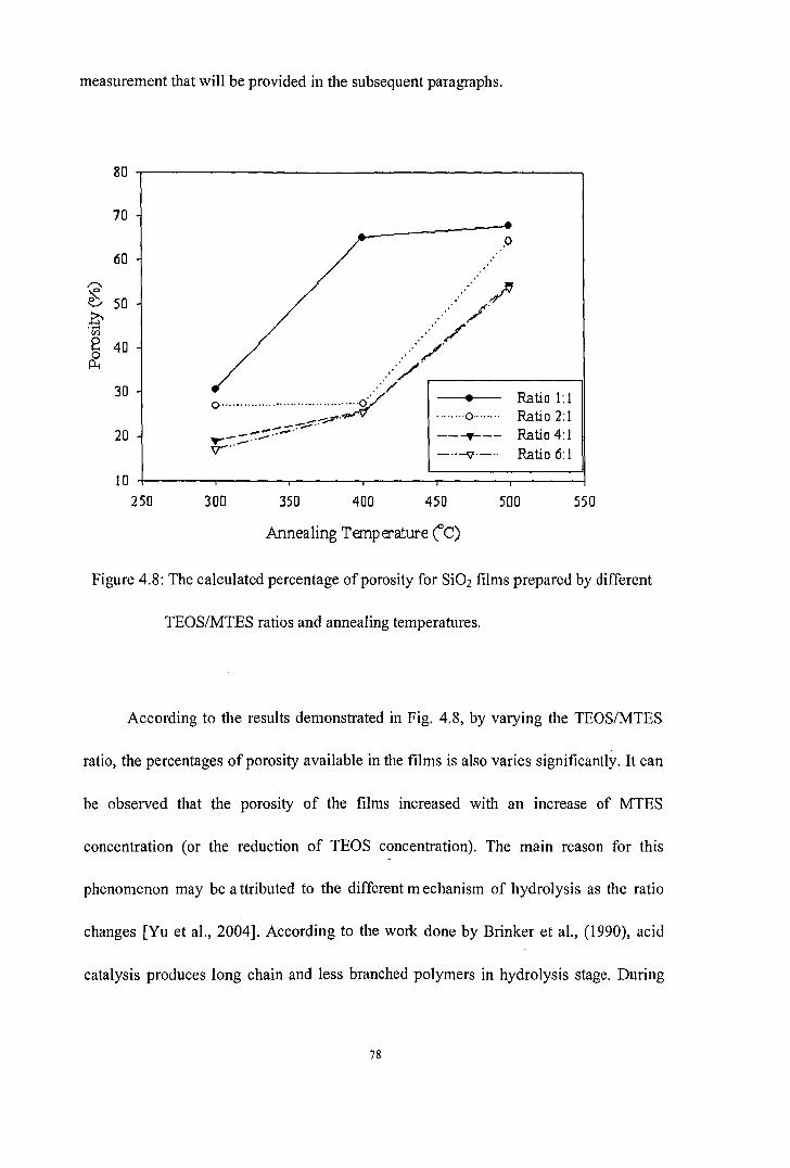
measurement that will be provided in the subsequent paragraphs.
.0
,/~.
. ,/..... /
..... /...../ .
..../ ...---------..,10 0·/ • Ratio 1:1
__.;::-.~_...A" ........ 0........ Ratio 2:1---:.-., Rati'o 4'.1~-_ .. - ---T---
'ir'" _ ......."._.. Ratio 6:1
80
70
60,,-..,~ 50e..-O'Vl8 400
Poi
30
20
10250 300 350 400 450 500 550
Annealing Temperature re)
Figure 4.8: The calculated percentage of porosity for SiOz films prepared by different
TEOS/MTES ratios and annealing temperatures.
According to the results demonstrated in Fig. 4.8, by varying the TEOS/MTES
ratio, the percentages of porosity available in the films is also varies significantly. It can
be observed that the porosity of the films increased with an increase of MTES
concentration (or the reduction of TEOS concentration). The main reason for this,
phenomenon may be a ttributed to the different mechanism of hydrolysis as the ratio
changes [Yu et al., 2004]. According to the work done by Brinker et al., (1990), acid
catalysis produces long chain and less branched polymers in hydrolysis stage. During
78

condensation stage, due to the low reaction rate, the film has sufficient time to
cross-link and form a dense gel. Therefore, pore volume and pore size in the formed
film is low. On the other hand, in a base catalysis process, it may produce highly
branched polymers during hydrolysis stage. Hence, in the condensation rate is fast, and
the growth tends to form spherically expanding clusters (particles). Therefore, the
formed film has higher porosity compared with a film produced using an acid catalyze.
In this work, the TEOS was catalyzed by an acid catalyze while the MTES was
catalyzed by base substance; thus, a composite structure with highly porous clusters
embedded into a dense matrix was formed. The MTES that was catalyzed by base can
be regarded as a pore generator in the broadest sense. Hence, as the molar fraction of
MTES increases, the amount of porous cluster is also increases and resulting in an
increase in porosity.
The calculated dielectric constant, k, as a function of annealing temperature and
TEOS/MTES ration is presented in Fig. 4.9. In general, the k value reduces as the
annealing temperature increases. The dielectric constant of sample prepared by
TEOS/MTES ratio of 1: I and heat treated at 300 DC was 4.79. A significant reduction of
the k value (1.93) is observed as the annealing temperature is increased to 500 DC. As
the annealing temperature increases, the p~rcentage of porosity in the film is also
increased. There would be a large amount of air trapped (kair = 1.0) inside the pore. This
may attribute to the lowering of k value.
79

550
o
500
Ratio 1:1Ratio 2: 1Ratio 4: 1Ratio 6: 1
•
450
---T---_ ..-v._..
· .. ··· .. 0 .. ··· .. ·
400350
~'"
X'.'~'.
~,
~,....~"
.........~,...........~
300
5.0
4.5
..... 4.0~iil8 3.50CJ.--tl 3.0lJ)
Q).~
2.5
2.0
1.5
250
Annealing TemperabJre \,C)
Figure 4.9: The calculated dielectric constant as a function of annealing temperature and
TEOS/MTES ratio.
4.3 Characterization of Fourier Transform Infrared Spectroscopy (FTIR)
Sample with TEOS/MTES ratio of 4: 1and heat treated at 300 DC, 400 DC, and 500
DC were independently investigated using a FTIR system (Fig. 4.10). FTIR is used to
determine qualitative and quantitative chemical species and bonding of a film. From the
spectra obtained in Fig. 4.5, there are 3 strong infrared transmittance peaks at around
1060 cm,l, 800 cm,l and 460 cm,l. These peak~ 1ire strongly associated with Si-O bonds
available in a silicon dioxide film. The peak around 1060 cm,l peak is the strongest and
it is attributed to a Si-O stretching bond. For thermal Si02, this peak is located at 1080
cm,l [Lau, 1999]. The shift of this peak as a function of annealing temperature is shown
80

in Fig. 4.11. The shift of the position is also accompanied by the change of full-width at
half-maximum (FWHM) of the peak (Fig. 4.12). When the annealing temperature
increases from 300 to 400 DC, the peak of Si-O-Si stretching bond is shifted to a higher
value; which is closer to 1080 em-I. However, there is a reduction in the FWHM of the
peak. Hence, we may conclude that a densification of the film is obtained as the
stretching of Si-O-Si bond is less in sample annealing at 400 DC if compared with 300
DC [Dimitrov et aI., 2000]. However, when the annealing temperature is further
increased to 500 DC, the position of the peak is shifted to a lower wave number; which is
further to 1080 em-I. At the same time, the FWHM value of the particular peak is
increased. This indicates that the stretching of Si-O-Si bond increases if compared with
the sample annealed at 4 00 Dc. During t his bond stretching process, it may generate
vacancy of oxygen atom. This vacancy may be treated as a donor like trap (st).
81
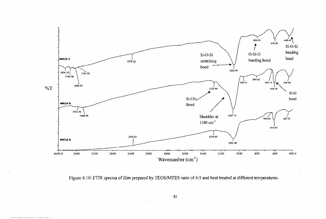
448.42'Si-O-Si
bending
bond
610.29
640.15 V, 44606
610.39 "" Si-Sibond
tO-Si-O
bending bond
Si-O-Si
stretching----~~bond
1063.00
1279.99
Shoulder at 1067.74
lIDO cm-1
Si_CH//.Bond
2378.22
3629.97
3572.50\
3468.94
400C(4.1)
%T
610.65
600C(4.1)1279.10
1064.40
4000.0 3600 3200 2800 2400 2000 1800 1600 1400
Wavenumber (em-I)1200 1000 800 600 400.0
Figure 4.10: FTIR spectra of film prepared by TEOSIMTES ratio of 4: 1 and heat treated at different temperatures.
82

1068
1067
,,-,.-I 1066Su
'--'....~
.0 1065S::l
=~;>
1064~
1063
1062250 300 350 400 450 500 550
Annealing Temperature (0C)
Figure 4.11: Location of peak due to Si-O-Si stretching bond as a function of annealing
temperature.
130,,-,.
E::l 125E.~
::E 1204.!.~::r: 115....ro..s::....'" 110~..!.."5 105~'--'
::E::r: 100~~
95250 300 350 4''00 450 500 550
Annealing Temperature (0C)
Figure 4. 12: FWHM value of the transmittance peak of Si-O-Si stretching bond as a
function ofannealing temperature.
83

From the transmittance spectra shown in Fig. 4.10, a shoulder is detected around
1100 to 1200 cm- I. This shoulder is corresponding to the longitudinal optical (LO)
vibration of Si-O-Si linkage. The appearance of this LO shoulder is due to the optical
scattering effect of porous sample [Yu et al., 2004].
Besides the transmittance peak located a round 1060 cm"I, t here are additional
two peaks associated with Si-O bonds. The peaks located at around 800 cm-1 and 460
cm"1 are attributed to bending of O-Si-O and Si-O-Si bonds [Lau, 1999]. The presence
of bending bonding O-Si-O is caused by hydrolysis process from the sample.
Meanwhile, the previous mentioned stretching bonding of Si-O-Si is attributed to the
condensation process; which involving the hydroxyls group and subsequently initial the
formation of inorganic polymer containing of Si-O-Si bond. Besides transmittance
peaks related to SiOz, peaks associated with Si substrate and incomplete or
contamination of organic substances have been detected at location a round 610 cm- I
(Si-Si bond) and >2300 cm-I (2340 cm-I, 3400 cm-I and 3600 cm"1 is related to Si-CH3,
Si-H, and stretching of O-H, respectively) [Kim, 1997 and Lau, 1999]. As the annealing
temperature increases, the later peak is reduced until it was not detected in sample
treated at 500°C.
4.3 Characterization of X-Ray Diffraction (XRD)
The x-ray diffractor graph of sample prepared by TEOS/MTES ratio of 4: 1 and
annealed at 3 00, 400 and 500°C is showed in Fig. 4.13. The result is matched with
84

phase and structure of Si02 using a JCPDS file for Si02 (file number = 5-0490). There
are two obvious peaks at 44.35° and 68.99° detected in sample annealed at 300 DC.
These peaks are associated with Si02 with (200) and (203) orientations. As the
annealing temperature increases, the later orientation of Si02 is reduced and eventually
disappeared.
SiOz (200) SiOz (203)'110 .. .._ ......_.~ ..._ ....... .. • __ ._ 500°C
.0'V)o -........ ~---.- ..- , ,. _ _-""''''- " 400°C
~
300°C
o 20 40 60
28 (Degree)
80 100 120
Figure 4.13: Pattern of XRD measured in sample prepared by TEOS/MTES ratio of
4: 1 and anneal at 300 DC, 400 DC and 500 DC.
The crystallite size of Si02, for the film, at a particular orientation can be
estimated using Scherrer equation [Eq. (4.5)].
85
(4.5)

where k is Scherrer constant, A is wavelength of x-ray radiation, Bilkl is Bragg angle,
and fJhkl is half intensity width measure in radian. In this work the crystallite size at
(2000 orientation has been estimated. The intensity of the peak at (200) is shown in Fig
4.9. It can be observed that the intensity increases from 300 to 400°C and beyond that
annealing temperature, the intensity is reduced. Figure 4.15 shows the effect of
annealing temperature on the crystallite size. The trend of crystallite size as a function
of annealing temperature is the same as the one revealed in Fig. 4.13. The crystallite
size increases as the annealing temperature increased from 300 to 400°C and further
increase of temperature he size is reduced significantly. It has been reported that when
the annealing temperature is higher t han a critical value, t he grain or crystallite size
drops down rapidly and vice versa and the annealing temperature is lower than the
critical value [He at el., 2005]. When the annealing temperature is lower than the
critical value, the density of nucleation is low. This may promote the growth of
crystallite or grain size [He et al., 2005].
86

28
26
24
,0 22'Vit::<I).....t:: 20-.
18
16
14
250 300 350 400 450
Annealing Temperature (oC)
500 550
Figure 4.14: Effect of annealing temperature on intensity for Si02 with
orientation (200).
3.2
3.0
-..2.8§
b 2.6.-'-'
<I)
.~ 2.4r:/J<I)
,";::- 2.2Ci3.....enC 2.0U
1.8
1.6
250 300 350 400 450
Annealing Temperature (OC)500 550
Figure 4.15: Effect of annealing temperature on the crystallite size.
87

When the annealing temperature of the film is higher than the critical value, there
are two possible mechanisms that may cause the decrease in crystallite size. One is the
oxygen deficiency in the Si02 thin films. When the annealing temperature is beyond the
critical value, the concentration of oxygen is super-saturated and attributed to an oxygen
deficit in the oxide layer. As a result, a high density of planar defect (grain boundaries)
appears in the film and it restricts the grain growth process [He et ai., 2005]. Hence, a
smaller crystallite size is observed. This explanation is in agreement with the wave
number shift of transmittance peak around 1060 cm- l for sampleannealedat500 °c
(Fig. 4.14). The other mechanism that may attribute to the reduction of crystallite size as
temperature is beyond a critical value is the high nucleation density. The nucleation of
complex oxide requires a sufficient energy to overcome chemical-reaction barrier. This
may be possible with higher annealing temperature. During this high annealing process,
clustering of stable crystallite is initiated and this combination of clusters acts as
nucleation sites for the growing of thin film. Since the high annealing temperature
promotes the clustering, a higher density of nuclei is obtained and this high density of
nuclei restricts the further growth of grain or crystallite size [He et ai., 2005]. The
subsequent sub-section shows the procedure of calculating the crystallite size.
Example orcalcnlation:
The sample is annealed at 500°C and prepared by TEOS/MTES ratio of 4: 1.
From Fig 4.14, k = 0.9
Ie = 1.54
88

Bilkl = 0.8400
f3i1kl = 44.34 I 2 = 22.17°
k:tFrom Eg. (4.5), L ilkl =----
f3i1kl cos Bilkl
= 0.9(1.54xlO-lO)
0.84(cos22.17)
The study of phase and orientation changes in Si02 prepared by different ratio
of TEOS I MTES heat treated at 400°C is showed in Fig. 4.16. It has been reveal that
the Si02 (200) oriented peak at 44.35° is independent of TEOS/MTES ratio. However,
the other peak related to Si02 (031) is the ratio dependence. This peak increases as the
concentration ofTEOS increases (or the MTES decreases). This is because TEOS is the
source of Si-O. If the concentration of TEOS reduces, this may affect the formation of
the Si-O-Si structure.
89

Si02 (031)
!
Sio, (200) I~~_..--J,--_J~_~u. 6:1
~f~I..w..-)~ __....~...... _ 4:1
,.~ .. ~~,_.._. . .i .~.;-;~""':tr~~~~.~~,....,~~~.;K.~'·~ .......1t•....,;~..-.fI_":"-r-t' 2: 1
~ ..._,.... l. .. .~~--- ]:1
o 20 40 60
26 (Degree)
80 100 120
Figure 4.16: Pattern of XRD for samples prepared by different TEOS/MTES ratio (1: 1,
2: 1. 4: 1, and 6: 1) and heat treated at 400°C.
4.4 Characterization ofAtomic Force Microscopy ( AFM )
AFM is used to investigate the surface topography of the thin film. Surface
topographies of sample prepared by TEOSIMTES ratio of 4: 1 and annealed at different
temperatures are presented in FigsA.17 to 4.19.
90

Figure 4.17: Surface topography of sample annealed at 300°C.
["'''1
Figure 4.18: Surface topography of sample annealed at 400°C.
91

[J.W'n]
Figure 4.19: Surface topography of sample annealed at 500°C.
The result qualitatively revealed that annealing temperature would change the
topography of the film. Quantitatively, root-mean-square roughness (RMS), n point
mean height (Rz), and surface mean height (Ra) of the investigated surfaces have been
extracted and their results are presented in Figs. 4.20, 4.21, and Fig 4.22, respectively.
5.0"""'Sc:b 4.5......'-'til
~ 4.0
'"rJl(1)
.Ebl) 3.5::l0
t:l:::(1)
!a 3.06-til
~ 2.5(1)
::E"00
t:l::: 2.0250 300 350 400 450 500 550
Annealing Temperature (oC)
Figure 4.20: Effect of annealing temperature on root-mean-square roughness (RMS) of
the film surface.
92

2.4
2.2----Ec'-' 2.0~...r...c
1.8OJ)
'v::r:c 1.6~Q)
:E.....c 1.4'00..c
1.2
1.0250 300 350 400 450
Annealing Temperature (0C)500 550
Figure 4.21: Effect of annealing temperature on n point mean height (Rz) of film
surface.
4.0
----Ec 3.50.....'-'
~ 3.0.....~...con'v::r:c 2.5~Q)
:EQ)()
~ 2.0....:l
r/)
5505004504003503001.5 -t------,----,-----.,.-----,,----,----j
250
Annealing Temperature COC)
Figure 4.22: Effect of annealing temperature on surface mean height (Ra) of the film
surface.
93

The value of RMS, Rz, and Ra are increased with the increase of annealing
temperature. The change of surface structure a nd topography a re obviously 0 bserved
when the temperature increased from 300 DC to 500DC. The surface of the film becomes
rougher as the annealing temperature increases may attribute to the grain growth
process [Tian et al., 2005].
4.5 Characterization of Scanning Electron Microscopy (SEM)
Figure 4.23 shows a SEM micrograph of a sample prepared by T EO/MTES
ratio of 4: 1 and annealed at 400 DC. The magnification of the image is 10,000 X. There
is no obvious grain, microstructure, and pore in the image. This indicates that the film is
covered well on the Si substrate. The same observations have been recorded for those
samples annealed at 300 and 500 DC.
Figure 4.23: SEM micrograph of sample prepared by TEOS/MTES ratio of 4: 1 and
annealed at 400 DC.
94

4.6 Characterization of Energy Dispersive X-Ray Analysis (EDX)
From the EDX result, elements of Si, 0, have been detected and C for samples
prepared by TEOS/MTES ratio of4: I and annealed at different temperatures (Fig. 4.24).
Since the results of FTIR and XRD revealed that the films are Si02, therefore we could
confirm that the Si and 0 elements are originated from Si02• The presence of C element
may due to the organic precursor source used in this work. Based on the EDX result, it
is clear that a slight reduction of 0 weight percent has been detected in sample annealed
at 500°C. This indicates oxygen deficiency and it is in agreement with the explanation
given in the section ofFTIR and XRD results [He et al., 2005].
0 0
0
~----- -----~-------T-------
80
70
tiD
50~.....,ib 40'v~
30
20
10
0250 300 350 400 450 500 550
Annealing"Temperature COC)
Figure 4.24: Weight percentage of various elements detected in samples with
TEOS I MTES ratio of 4: I and annealed at different temperatures.
95

4.7 Characterization of Electrical Property
I-V test has been performed on the film with TEOS/MTES ratio of 4:1 and
annealed at different temperatures. This test is to investigate the insulating property of
the film as a function of applied voltage. Stoneham et aI., (2005) stated that dielectric
film should have low leakage current in order to act as good insulator. The evolution of
the I-V characteristics with applied voltage indicates that different conduction
mechanisms occur depending on annealing temperature. The leakage current
mechanisms commonly reported in dielectric thin films include ohmic coriduction
(usually at low field), space-charge-limited conduction (SCLC), Poole-Frenkel
conduction, and Schottky conduction [Yang et aI., 2004]. Measurement of I-V curve
was done using two methods. The first one is to investigate the I-V characteristics of a
nano-region of the sample using a conductive atomic force microscope (C-AFM). While
the other method is to investigate the micro-region of the sample using a I-V meter.
The obtained I-V measurements are transformed into current density-electric field
(J-E) plots based on Eqs. (4.6) and (4.7). The equations are as follow:
Density current, J = I I A
where I is current in Ampere (A) unit and A is area in cm2 unit
Electric field, E == V I tox
96
(4.6)
(4.7)

where V is applied voltage in MV unit and tax is oxide thickness in cm unit.
A sample of calculation is provided in the following sub-section.
Example orcalcnlation:
Sample annealed at 500°C:
Density current, J = I / A
= 2.40 x 10.9 /4.908 x 10.12 cm2
= 488.99 A / cm2
Electric field, E == V / tox
== (3.52 x 1 x 10-6 MV) /120 x 10-7 cm
== 0.29MV / cm
Figure 4.25 shows the I-V plot of nano-region obtained from C-AFM. It is
obvious that leakage current reduces as the annealing temperature increases. Leakage
current at 80 V for film treated at 300°C is about 4.05 nA, it is reduced to 3.75 nA at
400°C, and 3.52 nA at 500°C. This result proven that the electrical property of the film
can be improved by increasing the annealing temperature.
97

5,.--------------------------,
4
3
o
-+- 300°C
·.. ·0···· 4000C
--T- 500°C
-1 -'------,------,------,r-------,------,r-----j
o 2 4 6 8 10
Voltage (xIOV)
Figure 4.25: Current-voltage characteristics of nano-region of sample prepared by
TEOS/MTES of 4: 1 and annealed at different temperatures.
Similar trend of the leakage current as a function of annealing temperature has
been revealed for micro-region samples (Fig. 4.26). When annealing temperature
increases, the density current is reduced. This indicates that leakage current is also
reduced. The current density at 0.41 MV/cm for sample annealed at 300°C is about
-1.119 A/cm2, it reduced to -4.469 A/cm2 at 400°C, and -4.832 A/cm2 at 500°C. The
,breakdown field of the investigated film has been extracted from the J-E plots. This
field refers to an instantaneous increase of J value at a particular electric field. It is
obvious that sample annealed at 400 and 300°C have demonstrated a sharp increase of J
at 0.58 and 0.38 MV/cm, while there is no significant increase in sample annealed at
98
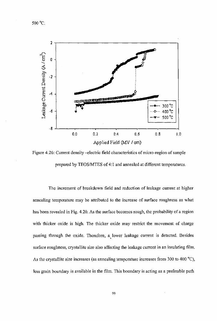
500 DC.
2
...........Ne 0u
.......
5~.til -2!D~
~
~ -4
uQ)onas~ -0asQ)
...:l
___ 300 DC
····0···· 400 DC- .....- 500 DC
-8 -1.------,------,------,------,------,-----1
0.0 0.2 0.4 0.6 0.8 1.0
Applied Field (l:vfV I em)
Figure 4.26: Current density -electric field characteristics of micro-region of sample
prepared by TEOS/MTES of 4: 1 and annealed at different temperatures.
The increment of breakdown field and reduction of leakage current at higher
annealing temperature may be attributed to the increase of surface roughness as what
has been revealed in Fig. 4.20. As the surface becomes rough, the probability of a region
with thicker oxide is high. The thicker oxide may restrict the movement of charge
passing through the oxide. Therefore, a lower leakage current is detected. Besides,
surface roughness, crystallite size also affecting the leakage current in an insulating film.
As the crystallite size increases (as annealing temperature increases from 300 to 400 DC),
less grain boundary is available in the film. This boundary is acting as a preferable path
99

for current conduction. When this boundary reduces, the probability of current passing
through this path is being reduced and its leakage current is also reduced. However, for
sample annealed at 500 DC, crystallite size does not play a main role to reduce the
leakage current. As at this annealing temperature, the produced film has demonstrated a
deficiency of oxygen as being proven by EDX and also suggested by FTIR. This may
act as a donor-like trap for the injected electron. As the electron being injected from Si
into the oxide, majority of the electron is captured and neutralized in the trap. This is not
happening in samples annealed at 300 and 400 Dc. Therefore, the leakage current is
much lower than those samples.
100

CHAPTER 5: CONCLUSION AND SUGGESTION
This chapter presents the research conclusion of the effect of temperature and
TEOS/MTES ratio of precursor for the sol-gel derived low dielectric ocnstant Si02 thin
film on Si.
5.1 Conclusion
Uniform low dielectric constant silica thin films were fabricated using'sol-gel
process. The processing temperature had great effect on the physical and electrical
properties of the films. With increasing annealing temperature, percentage of porosity
has been increased while the dielectric constant and refractive index has been decreased.
FTIR, XRD, and EDX results have shown that the deposited thin film is Si02• The high
value of RMS and Rz as well as the donor-like trap in the bulk oxide for sample
annealed at 500 DC was the main caused of the low leakage current.
5.2 Suggestions for future research
1. The annealing process can be replaced by rapid thermal processes (RTP) so that
a better control of the ambient condition.
11. The result of thickness and refractive index that has been measured by
Filmetrics should be re-confirmed by an ellipsometer.,
111. Methyltrimethoxysilane (MTMS) and dimethylchlorosilane (DMCS) could be
used to replace MTES as organic precursor.
101

\ '
REFERENCES
Brinker, C.1. & Scherer, GW. (1990). 'Sol-Gel Science' Academic Press, New York.
Dimitrov. D. B, Beshkova. M & Dafinova. R, (2000), Infuence of vacuum rapidthermal annealing on the properties of~PCVD Si02and Si02.P20 s films, Vacuum, 58,pp.485-489.
Ghandhi, (1994), VLSI Fabrication Principles (Silicon and Gallium Arsenide),Second Edition, Wiley Interscience, United State ofAmerica.
Glaser. P. M & Pantano. C. G, (1984), Effect of the H20/TEOS Ratio upon thePreparation and Nitridation of Silica Sol-gel Films, Journal of Non-Crystalline Solids,63, pp. 209-221.
He. S, Li. Y, Liu. X, Tao. B, Li. D & Lu. Q, (2005), Correlations between grain sizeand nonlinear dielectric properties of as-deposited SrTi03 thin films, Thin Solid Films,478, pp. 261-264.
He. Z. W, Liu. X. Q, Xu. D. Y & Wang. Y. Y, (2006), Effect of annealing on theproperties of low-k nanoporous Si02 films prepared by sol-gel method with catalystHF, Microelectronics Reliability, 46, pp. 2062-2066.
Hong. 1. K, Yang. H. S, Jo. M. H, Park. H. H & Choi. S. Y, (1997), Preparation andcharacterization of porous silica xerogel film for low dielectric application, Thin SolidFilms, 308-309, pp. 495-500.
Jones. S. W, IC knowledge, (2000), "History of the integrated circuit" I
http://www.icknowledge.com/history/1960s.html. 25 Feb 2007.
Kim. M. T, (1997), Deposition behavior of hexamethydisiloxane films based on theFTIR analysis of Si-O-Si and Si-CH bonds, Thin Solid Films, 311, pp.157-l63.
Klein. L. C, (1991), 'Sol-gel coatings', in 'JL Vossen & W Kern (eds), Thin Film. Processes II, pp. 501-520, United States of America: Academic Press.
Lau. W. S, (1999), Infrared Characterization for Microelectronics, World ScientificPublishing, pp.56-56.
Li. Z. J, Lew. C. M, L i. S, Medina. D. I & Yan. Y. S, (2005), Pure-Silica-ZeoliteMEL Low-k Films from Nanoparticle Suspensions, 1. Phys. Chern. B, 109, pp.
103

8652-8658.
Lisa, C.K (1988). Sol-gel technology for thin films, fibers, performs, electronics andspecialty shapes. New Jersey: Noyes Publications.
Manjari. E. A, Subrahmanyam. A, DasGupta. N, & DasGupta. A, (2002), ElecticalCharacterization of Metal-Insulator-Semiconductor Capacitors with Xerogel asDielectric, Applied Physics Letters, 80(10), pp. 1800-1802.
May. G. S & Sze. S. M, (2002), Fundamentals of Semiconductor Fabrication, 1sl
Edition, John Wiley & sons, United State of America.
Rao. A. V & Kalesh. R. R, (2004), Comparative studies of the physical andhydrophobic properties of TEaS based silica aerogels using different co-precursors,
Science and Technology of Advanced Materials.
Regnier. C, Tristant. P, Desmaiso. J, (1996), Remote microwave plasma-enhancedchemical vapour deposition of insulating coatings (Si02) on metallic substrates: film
properties, Surface and Coatings Technology, 80, pp.18-22.
Risch, (2006), Pushing CMOS beyond the roadmap, Solid-State Electronics, 50, pp.527-535.
Runyan. W. R & Shaffner. T. J, (1997), Semiconductor measurements &instrumentation, 2nd edn, United States of America: McGraw-Hill.
Ruzyllo. J, (2003), High-k dielectric? Low-k dielectric? Semiconductor N otes,Note
No 1.
Seraji. S, Wu. Y, Forbess. M, Limmer. S. J, Chou. T & Cao. C. Z, (2000),
Sol-Gel-Derived Mesoporous Silica Films with Low Dielectric Constants, AdvancedMaterials, 12, No. 22, pp. 1695-1698.
Shamiryan, D, Abell, T, Iacopi, F & Maex, K, (2004), Low-k dielectric materials,Materials Today, Volume 7, Issue 1, pp. 34-39.
Sze, S, M, (2002), Semiconductor Devices, 2nd Edition, John Wiley & sons, United
State of America.
Tian. G. L., Dong. L., Wei. C. Y, Huang. J. B., He. H. B & Shao. J. B, (2006),Investigation on microstructure and optical properties of titanium dioxide coatings
annealed at various temperature, Optical Materials, 28, pp.1058-1063.
104

Vasudev, P, K, (1996), CMOS Device and Interconnect Technology Enhancementsfor Low Power/Low Voltage Application, Solid-State Electronics Vol. 39, No.4, pp.481-488.
Warren. W. L, Lenahan. P. M, Brinker. C. J, Ashley. C. S & Reed. S. T, (1991),Sol-Gel Silicate Thin Film Electronic Properties, J. Appl. Phys., 69(8), pp.4404-4408.
Weimer. R .A, Brinker. C. J, Lenahan. P. M & Marchione. T .A, (1987), ElectronicProperties of Sol-Gel Derived Oxides on Silicon, Appl. Phys. Lett, 51 (15).
Wilson. S. R, Tracy. C. J & Freeman. 1. L, (1993), Multilevel MetallizationTerminology and Sructure, Handbook of Multilevel Metallization for IntegratedCircuits, 1st Edition, Chapter 1, Wilson. S. R, Tracy. C. J & Freeman. J. L, NoyesPublications, United State of America.
Yang. X, Huang. B, Wang. H, Shang. S, Yao. W & Wei. J, (2004), Leakage currentbehavior of La-doped BhThO? thin films by a chemical solution deposition method,Materials Letters, 58, pp-3725- 3728.
Yu. S, Wong. K.S, Hu. X, Goh. T, K, (2004), Effect of processing temperature on theproperties of sol-gel-derived mesoporous silica films, Thin Solid Films 462-463, pp.306- 310.
Yu. S, Wong. K.S, Hu. X, Pita. K, (2004), Sol-gel derived mesoporous silica filmsused as low dielectric constant materials, Thin Solid Films, 462-463, pp. 311 -315.
105