Embed Size (px)
Citation preview

LAN8710A/LAN8710Ai
Small Footprint MII/RMII 10/100 Ethernet Transceiver with HP Auto-MDIX and flexPWR® Technology
DatasheetPRODUCT FEATURES
Highlights
Single-Chip Ethernet Physical Layer Transceiver (PHY)Comprehensive flexPWR® Technology — Flexible Power Management Architecture— LVCMOS Variable I/O voltage range: +1.6V to +3.6V— Integrated 1.2V regulator with disable featureHP Auto-MDIX supportSmall footprint 32-pin QFN lead-free RoHS compliant package (5 x 5 x 0.9mm height)
Target Applications
Set-Top BoxesNetworked Printers and ServersTest InstrumentationLAN on MotherboardEmbedded Telecom ApplicationsVideo Record/Playback SystemsCable Modems/RoutersDSL Modems/RoutersDigital Video RecordersIP and Video PhonesWireless Access PointsDigital TelevisionsDigital Media Adaptors/ServersGaming ConsolesPOE Applications (Refer to SMSC Application Note 17.18)
Key Benefits
High-Performance 10/100 Ethernet Transceiver— Compliant with IEEE802.3/802.3u (Fast Ethernet)— Compliant with ISO 802-3/IEEE 802.3 (10BASE-T)— Loop-back modes— Auto-negotiation— Automatic polarity detection and correction— Link status change wake-up detection— Vendor specific register functions— Supports both MII and the reduced pin count RMII
interfacesPower and I/Os— Various low power modes— Integrated power-on reset circuit— Two status LED outputs— Latch-Up Performance Exceeds 150mA per EIA/JESD
78, Class II— May be used with a single 3.3V supplyAdditional Features— Ability to use a low cost 25Mhz crystal for reduced BOMPackaging— 32-pin QFN (5x5 mm) Lead-Free RoHS Compliant
package with MII and RMIIEnvironmental— Extended commercial temperature range
(0°C to +85°C)— Industrial temperature range version available
(-40°C to +85°C)
SMSC LAN8710A/LAN8710Ai Revision 1.4 (08-23-12)
DATASHEET

Small Footprint MII/RMII 10/100 Ethernet Transceiver with HP Auto-MDIX and flexPWR® Technology
Datasheet
Order Numbers:LAN8710Ai-EZK for 32-pin QFN lead-free RoHS compliant package (-40 to +85°C temp)
LAN8710Ai-EZK-TR for 32-pin QFN lead-free RoHS compliant package (-40 to +85°C temp)LAN8710A-EZC for 32-pin QFN lead-free RoHS compliant package (0 to +85°C temp)
LAN8710A-EZC-TR for 32-pin QFN lead-free RoHS compliant package (0 to +85°C temp)
TR indicates tape & reel option. Reel size is 4,000.
This product meets the halogen maximum concentration values per IEC61249-2-21
For RoHS compliance and environmental information, please visit www.smsc.com/rohs
Please contact your SMSC sales representative for additional documentation related to this product such as application notes, anomaly sheets, and design guidelines.
Revision 1.4 (08-23-12) 2 SMSC LAN8710A/LAN8710Ai
Copyright © 2012 SMSC or its subsidiaries. All rights reserved.Circuit diagrams and other information relating to SMSC products are included as a means of illustrating typical applications. Consequently, complete information sufficient forconstruction purposes is not necessarily given. Although the information has been checked and is believed to be accurate, no responsibility is assumed for inaccuracies. SMSCreserves the right to make changes to specifications and product descriptions at any time without notice. Contact your local SMSC sales office to obtain the latest specificationsbefore placing your product order. The provision of this information does not convey to the purchaser of the described semiconductor devices any licenses under any patentrights or other intellectual property rights of SMSC or others. All sales are expressly conditional on your agreement to the terms and conditions of the most recently datedversion of SMSC's standard Terms of Sale Agreement dated before the date of your order (the "Terms of Sale Agreement"). The product may contain design defects or errorsknown as anomalies which may cause the product's functions to deviate from published specifications. Anomaly sheets are available upon request. SMSC products are notdesigned, intended, authorized or warranted for use in any life support or other application where product failure could cause or contribute to personal injury or severe propertydamage. Any and all such uses without prior written approval of an Officer of SMSC and further testing and/or modification will be fully at the risk of the customer. Copies ofthis document or other SMSC literature, as well as the Terms of Sale Agreement, may be obtained by visiting SMSC’s website at http://www.smsc.com. SMSC is a registeredtrademark of Standard Microsystems Corporation (“SMSC”). Product names and company names are the trademarks of their respective holders.
The Microchip name and logo, and the Microchip logo are registered trademarks of Microchip Technology Incorporated in the U.S.A. and other countries.SMSC DISCLAIMS AND EXCLUDES ANY AND ALL WARRANTIES, INCLUDING WITHOUT LIMITATION ANY AND ALL IMPLIED WARRANTIES OF MERCHANTABILITY,FITNESS FOR A PARTICULAR PURPOSE, TITLE, AND AGAINST INFRINGEMENT AND THE LIKE, AND ANY AND ALL WARRANTIES ARISING FROM ANY COURSEOF DEALING OR USAGE OF TRADE. IN NO EVENT SHALL SMSC BE LIABLE FOR ANY DIRECT, INCIDENTAL, INDIRECT, SPECIAL, PUNITIVE, OR CONSEQUENTIALDAMAGES; OR FOR LOST DATA, PROFITS, SAVINGS OR REVENUES OF ANY KIND; REGARDLESS OF THE FORM OF ACTION, WHETHER BASED ON CONTRACT;TORT; NEGLIGENCE OF SMSC OR OTHERS; STRICT LIABILITY; BREACH OF WARRANTY; OR OTHERWISE; WHETHER OR NOT ANY REMEDY OF BUYER IS HELDTO HAVE FAILED OF ITS ESSENTIAL PURPOSE, AND WHETHER OR NOT SMSC HAS BEEN ADVISED OF THE POSSIBILITY OF SUCH DAMAGES.
DATASHEET
Small Footprint MII/RMII 10/100 Ethernet Transceiver with HP Auto-MDIX and flexPWR® Technology
Datasheet
Table of Contents
Chapter 1 Introduction . . . . . . . . . . . . . . . . . . . . . . . . . . . . . . . . . . . . . . . . . . . . . . . . . . . . . . . 71.1 General Terms and Conventions . . . . . . . . . . . . . . . . . . . . . . . . . . . . . . . . . . . . . . . . . . . . . . . . . . . 71.2 General Description . . . . . . . . . . . . . . . . . . . . . . . . . . . . . . . . . . . . . . . . . . . . . . . . . . . . . . . . . . . . . 7
Chapter 2 Pin Description and Configuration . . . . . . . . . . . . . . . . . . . . . . . . . . . . . . . . . . . . 92.1 Pin Assignments . . . . . . . . . . . . . . . . . . . . . . . . . . . . . . . . . . . . . . . . . . . . . . . . . . . . . . . . . . . . . . . 172.2 Buffer Types . . . . . . . . . . . . . . . . . . . . . . . . . . . . . . . . . . . . . . . . . . . . . . . . . . . . . . . . . . . . . . . . . . 18
Chapter 3 Functional Description . . . . . . . . . . . . . . . . . . . . . . . . . . . . . . . . . . . . . . . . . . . . . 193.1 Transceiver . . . . . . . . . . . . . . . . . . . . . . . . . . . . . . . . . . . . . . . . . . . . . . . . . . . . . . . . . . . . . . . . . . . 19
3.1.1 100BASE-TX Transmit . . . . . . . . . . . . . . . . . . . . . . . . . . . . . . . . . . . . . . . . . . . . . . . . . . 193.1.2 100BASE-TX Receive . . . . . . . . . . . . . . . . . . . . . . . . . . . . . . . . . . . . . . . . . . . . . . . . . . . 223.1.3 10BASE-T Transmit. . . . . . . . . . . . . . . . . . . . . . . . . . . . . . . . . . . . . . . . . . . . . . . . . . . . . 243.1.4 10BASE-T Receive . . . . . . . . . . . . . . . . . . . . . . . . . . . . . . . . . . . . . . . . . . . . . . . . . . . . . 25
3.2 Auto-negotiation . . . . . . . . . . . . . . . . . . . . . . . . . . . . . . . . . . . . . . . . . . . . . . . . . . . . . . . . . . . . . . . 263.2.1 Parallel Detection . . . . . . . . . . . . . . . . . . . . . . . . . . . . . . . . . . . . . . . . . . . . . . . . . . . . . . 273.2.2 Restarting Auto-negotiation . . . . . . . . . . . . . . . . . . . . . . . . . . . . . . . . . . . . . . . . . . . . . . . 273.2.3 Disabling Auto-negotiation. . . . . . . . . . . . . . . . . . . . . . . . . . . . . . . . . . . . . . . . . . . . . . . . 283.2.4 Half vs. Full Duplex . . . . . . . . . . . . . . . . . . . . . . . . . . . . . . . . . . . . . . . . . . . . . . . . . . . . . 28
3.3 HP Auto-MDIX Support. . . . . . . . . . . . . . . . . . . . . . . . . . . . . . . . . . . . . . . . . . . . . . . . . . . . . . . . . . 293.4 MAC Interface. . . . . . . . . . . . . . . . . . . . . . . . . . . . . . . . . . . . . . . . . . . . . . . . . . . . . . . . . . . . . . . . . 30
3.4.1 MII . . . . . . . . . . . . . . . . . . . . . . . . . . . . . . . . . . . . . . . . . . . . . . . . . . . . . . . . . . . . . . . . . . 303.4.2 RMII . . . . . . . . . . . . . . . . . . . . . . . . . . . . . . . . . . . . . . . . . . . . . . . . . . . . . . . . . . . . . . . . . 303.4.3 MII vs. RMII Configuration . . . . . . . . . . . . . . . . . . . . . . . . . . . . . . . . . . . . . . . . . . . . . . . . 31
3.5 Serial Management Interface (SMI) . . . . . . . . . . . . . . . . . . . . . . . . . . . . . . . . . . . . . . . . . . . . . . . . 333.6 Interrupt Management . . . . . . . . . . . . . . . . . . . . . . . . . . . . . . . . . . . . . . . . . . . . . . . . . . . . . . . . . . 34
3.6.1 Primary Interrupt System. . . . . . . . . . . . . . . . . . . . . . . . . . . . . . . . . . . . . . . . . . . . . . . . . 343.6.2 Alternate Interrupt System. . . . . . . . . . . . . . . . . . . . . . . . . . . . . . . . . . . . . . . . . . . . . . . . 35
3.7 Configuration Straps . . . . . . . . . . . . . . . . . . . . . . . . . . . . . . . . . . . . . . . . . . . . . . . . . . . . . . . . . . . . 363.7.1 PHYAD[2:0]: PHY Address Configuration . . . . . . . . . . . . . . . . . . . . . . . . . . . . . . . . . . . . 363.7.2 MODE[2:0]: Mode Configuration . . . . . . . . . . . . . . . . . . . . . . . . . . . . . . . . . . . . . . . . . . . 363.7.3 RMIISEL: MII/RMII Mode Configuration . . . . . . . . . . . . . . . . . . . . . . . . . . . . . . . . . . . . . 373.7.4 REGOFF: Internal +1.2V Regulator Configuration . . . . . . . . . . . . . . . . . . . . . . . . . . . . . 383.7.5 nINTSEL: nINT/TXER/TXD4 Configuration . . . . . . . . . . . . . . . . . . . . . . . . . . . . . . . . . . . 38
3.8 Miscellaneous Functions . . . . . . . . . . . . . . . . . . . . . . . . . . . . . . . . . . . . . . . . . . . . . . . . . . . . . . . . 393.8.1 LEDs . . . . . . . . . . . . . . . . . . . . . . . . . . . . . . . . . . . . . . . . . . . . . . . . . . . . . . . . . . . . . . . . 393.8.2 Variable Voltage I/O . . . . . . . . . . . . . . . . . . . . . . . . . . . . . . . . . . . . . . . . . . . . . . . . . . . . 403.8.3 Power-Down Modes . . . . . . . . . . . . . . . . . . . . . . . . . . . . . . . . . . . . . . . . . . . . . . . . . . . . 403.8.4 Isolate Mode . . . . . . . . . . . . . . . . . . . . . . . . . . . . . . . . . . . . . . . . . . . . . . . . . . . . . . . . . . 413.8.5 Resets . . . . . . . . . . . . . . . . . . . . . . . . . . . . . . . . . . . . . . . . . . . . . . . . . . . . . . . . . . . . . . . 413.8.6 Carrier Sense . . . . . . . . . . . . . . . . . . . . . . . . . . . . . . . . . . . . . . . . . . . . . . . . . . . . . . . . . 413.8.7 Collision Detect . . . . . . . . . . . . . . . . . . . . . . . . . . . . . . . . . . . . . . . . . . . . . . . . . . . . . . . . 423.8.8 Link Integrity Test . . . . . . . . . . . . . . . . . . . . . . . . . . . . . . . . . . . . . . . . . . . . . . . . . . . . . . 423.8.9 Loopback Operation . . . . . . . . . . . . . . . . . . . . . . . . . . . . . . . . . . . . . . . . . . . . . . . . . . . . 42
3.9 Application Diagrams . . . . . . . . . . . . . . . . . . . . . . . . . . . . . . . . . . . . . . . . . . . . . . . . . . . . . . . . . . . 443.9.1 Simplified System Level Application Diagram . . . . . . . . . . . . . . . . . . . . . . . . . . . . . . . . . 453.9.2 Power Supply Diagram (1.2V Supplied by Internal Regulator) . . . . . . . . . . . . . . . . . . . . 463.9.3 Power Supply Diagram (1.2V Supplied by External Source). . . . . . . . . . . . . . . . . . . . . . 473.9.4 Twisted-Pair Interface Diagram (Single Power Supply). . . . . . . . . . . . . . . . . . . . . . . . . . 483.9.5 Twisted-Pair Interface Diagram (Dual Power Supplies) . . . . . . . . . . . . . . . . . . . . . . . . . 49
SMSC LAN8710A/LAN8710Ai 3 Revision 1.4 (08-23-12)
DATASHEET

Small Footprint MII/RMII 10/100 Ethernet Transceiver with HP Auto-MDIX and flexPWR® Technology
Datasheet
Chapter 4 Register Descriptions . . . . . . . . . . . . . . . . . . . . . . . . . . . . . . . . . . . . . . . . . . . . . . . 504.1 Register Nomenclature . . . . . . . . . . . . . . . . . . . . . . . . . . . . . . . . . . . . . . . . . . . . . . . . . . . . . . . . . . 504.2 Control and Status Registers . . . . . . . . . . . . . . . . . . . . . . . . . . . . . . . . . . . . . . . . . . . . . . . . . . . . . 51
4.2.1 Basic Control Register . . . . . . . . . . . . . . . . . . . . . . . . . . . . . . . . . . . . . . . . . . . . . . . . . . . 524.2.2 Basic Status Register . . . . . . . . . . . . . . . . . . . . . . . . . . . . . . . . . . . . . . . . . . . . . . . . . . . 534.2.3 PHY Identifier 1 Register . . . . . . . . . . . . . . . . . . . . . . . . . . . . . . . . . . . . . . . . . . . . . . . . . 544.2.4 PHY Identifier 2 Register . . . . . . . . . . . . . . . . . . . . . . . . . . . . . . . . . . . . . . . . . . . . . . . . . 554.2.5 Auto Negotiation Advertisement Register . . . . . . . . . . . . . . . . . . . . . . . . . . . . . . . . . . . . 564.2.6 Auto Negotiation Link Partner Ability Register. . . . . . . . . . . . . . . . . . . . . . . . . . . . . . . . . 574.2.7 Auto Negotiation Expansion Register . . . . . . . . . . . . . . . . . . . . . . . . . . . . . . . . . . . . . . . 584.2.8 Mode Control/Status Register . . . . . . . . . . . . . . . . . . . . . . . . . . . . . . . . . . . . . . . . . . . . . 594.2.9 Special Modes Register. . . . . . . . . . . . . . . . . . . . . . . . . . . . . . . . . . . . . . . . . . . . . . . . . . 604.2.10 Symbol Error Counter Register . . . . . . . . . . . . . . . . . . . . . . . . . . . . . . . . . . . . . . . . . . . . 614.2.11 Special Control/Status Indications Register. . . . . . . . . . . . . . . . . . . . . . . . . . . . . . . . . . . 624.2.12 Interrupt Source Flag Register . . . . . . . . . . . . . . . . . . . . . . . . . . . . . . . . . . . . . . . . . . . . 634.2.13 Interrupt Mask Register . . . . . . . . . . . . . . . . . . . . . . . . . . . . . . . . . . . . . . . . . . . . . . . . . . 644.2.14 PHY Special Control/Status Register . . . . . . . . . . . . . . . . . . . . . . . . . . . . . . . . . . . . . . . 65
Chapter 5 Operational Characteristics . . . . . . . . . . . . . . . . . . . . . . . . . . . . . . . . . . . . . . . . . 665.1 Absolute Maximum Ratings*. . . . . . . . . . . . . . . . . . . . . . . . . . . . . . . . . . . . . . . . . . . . . . . . . . . . . . 665.2 Operating Conditions** . . . . . . . . . . . . . . . . . . . . . . . . . . . . . . . . . . . . . . . . . . . . . . . . . . . . . . . . . . 675.3 Power Consumption . . . . . . . . . . . . . . . . . . . . . . . . . . . . . . . . . . . . . . . . . . . . . . . . . . . . . . . . . . . . 675.4 DC Specifications . . . . . . . . . . . . . . . . . . . . . . . . . . . . . . . . . . . . . . . . . . . . . . . . . . . . . . . . . . . . . . 685.5 AC Specifications . . . . . . . . . . . . . . . . . . . . . . . . . . . . . . . . . . . . . . . . . . . . . . . . . . . . . . . . . . . . . . 70
5.5.1 Equivalent Test Load. . . . . . . . . . . . . . . . . . . . . . . . . . . . . . . . . . . . . . . . . . . . . . . . . . . . 705.5.2 Power Sequence Timing . . . . . . . . . . . . . . . . . . . . . . . . . . . . . . . . . . . . . . . . . . . . . . . . . 715.5.3 Power-On nRST & Configuration Strap Timing . . . . . . . . . . . . . . . . . . . . . . . . . . . . . . . . 725.5.4 MII Interface Timing. . . . . . . . . . . . . . . . . . . . . . . . . . . . . . . . . . . . . . . . . . . . . . . . . . . . . 735.5.5 RMII Interface Timing . . . . . . . . . . . . . . . . . . . . . . . . . . . . . . . . . . . . . . . . . . . . . . . . . . . 755.5.6 SMI Timing . . . . . . . . . . . . . . . . . . . . . . . . . . . . . . . . . . . . . . . . . . . . . . . . . . . . . . . . . . . 76
5.6 Clock Circuit . . . . . . . . . . . . . . . . . . . . . . . . . . . . . . . . . . . . . . . . . . . . . . . . . . . . . . . . . . . . . . . . . . 77
Chapter 6 Package Outline . . . . . . . . . . . . . . . . . . . . . . . . . . . . . . . . . . . . . . . . . . . . . . . . . . . 78
Chapter 7 Datasheet Revision History . . . . . . . . . . . . . . . . . . . . . . . . . . . . . . . . . . . . . . . . . . 81
Revision 1.4 (08-23-12) 4 SMSC LAN8710A/LAN8710Ai
DATASHEET
Small Footprint MII/RMII 10/100 Ethernet Transceiver with HP Auto-MDIX and flexPWR® Technology
Datasheet
SMSC LAN8710A/LAN8710Ai 5 Revision 1.4 (08-23-12)
DATASHEET
List of FiguresFigure 1.1 System Block Diagram. . . . . . . . . . . . . . . . . . . . . . . . . . . . . . . . . . . . . . . . . . . . . . . . . . . . . . . 8Figure 1.2 Architectural Overview . . . . . . . . . . . . . . . . . . . . . . . . . . . . . . . . . . . . . . . . . . . . . . . . . . . . . . . 8Figure 2.1 32-QFN Pin Assignments (TOP VIEW) . . . . . . . . . . . . . . . . . . . . . . . . . . . . . . . . . . . . . . . . . . 9Figure 3.1 100BASE-TX Transmit Data Path . . . . . . . . . . . . . . . . . . . . . . . . . . . . . . . . . . . . . . . . . . . . . 19Figure 3.2 100BASE-TX Receive Data Path. . . . . . . . . . . . . . . . . . . . . . . . . . . . . . . . . . . . . . . . . . . . . . 22Figure 3.3 Relationship Between Received Data and Specific MII Signals . . . . . . . . . . . . . . . . . . . . . . 24Figure 3.4 Direct Cable Connection vs. Cross-over Cable Connection . . . . . . . . . . . . . . . . . . . . . . . . . 29Figure 3.5 MDIO Timing and Frame Structure - READ Cycle. . . . . . . . . . . . . . . . . . . . . . . . . . . . . . . . . 33Figure 3.6 MDIO Timing and Frame Structure - WRITE Cycle . . . . . . . . . . . . . . . . . . . . . . . . . . . . . . . . 33Figure 3.7 LED1/REGOFF Polarity Configuration. . . . . . . . . . . . . . . . . . . . . . . . . . . . . . . . . . . . . . . . . . 39Figure 3.8 LED2/nINTSEL Polarity Configuration . . . . . . . . . . . . . . . . . . . . . . . . . . . . . . . . . . . . . . . . . . 40Figure 3.9 Near-end Loopback Block Diagram . . . . . . . . . . . . . . . . . . . . . . . . . . . . . . . . . . . . . . . . . . . . 43Figure 3.10 Far Loopback Block Diagram. . . . . . . . . . . . . . . . . . . . . . . . . . . . . . . . . . . . . . . . . . . . . . . . . 43Figure 3.11 Connector Loopback Block Diagram . . . . . . . . . . . . . . . . . . . . . . . . . . . . . . . . . . . . . . . . . . . 44Figure 3.12 Simplified System Level Application Diagram . . . . . . . . . . . . . . . . . . . . . . . . . . . . . . . . . . . . 45Figure 3.13 Power Supply Diagram (1.2V Supplied by Internal Regulator) . . . . . . . . . . . . . . . . . . . . . . . 46Figure 3.14 Power Supply Diagram (1.2V Supplied by External Source) . . . . . . . . . . . . . . . . . . . . . . . . . 47Figure 3.15 Twisted-Pair Interface Diagram (Single Power Supply) . . . . . . . . . . . . . . . . . . . . . . . . . . . . . 48Figure 3.16 Twisted-Pair Interface Diagram (Dual Power Supplies). . . . . . . . . . . . . . . . . . . . . . . . . . . . . 49Figure 5.1 Output Equivalent Test Load . . . . . . . . . . . . . . . . . . . . . . . . . . . . . . . . . . . . . . . . . . . . . . . . . 70Figure 5.2 Power Sequence Timing . . . . . . . . . . . . . . . . . . . . . . . . . . . . . . . . . . . . . . . . . . . . . . . . . . . . 71Figure 5.3 Power-On nRST & Configuration Strap Timing . . . . . . . . . . . . . . . . . . . . . . . . . . . . . . . . . . . 72Figure 5.4 MII Receive Timing . . . . . . . . . . . . . . . . . . . . . . . . . . . . . . . . . . . . . . . . . . . . . . . . . . . . . . . . 73Figure 5.5 MII Transmit Timing . . . . . . . . . . . . . . . . . . . . . . . . . . . . . . . . . . . . . . . . . . . . . . . . . . . . . . . . 74Figure 5.6 RMII Timing . . . . . . . . . . . . . . . . . . . . . . . . . . . . . . . . . . . . . . . . . . . . . . . . . . . . . . . . . . . . . . 75Figure 5.7 SMI Timing . . . . . . . . . . . . . . . . . . . . . . . . . . . . . . . . . . . . . . . . . . . . . . . . . . . . . . . . . . . . . . . 76Figure 6.1 32-QFN Package . . . . . . . . . . . . . . . . . . . . . . . . . . . . . . . . . . . . . . . . . . . . . . . . . . . . . . . . . . 78Figure 6.2 Recommended PCB Land Pattern. . . . . . . . . . . . . . . . . . . . . . . . . . . . . . . . . . . . . . . . . . . . . 79Figure 6.3 Taping Dimensions and Part Orientation . . . . . . . . . . . . . . . . . . . . . . . . . . . . . . . . . . . . . . . . 79Figure 6.4 Reel Dimensions . . . . . . . . . . . . . . . . . . . . . . . . . . . . . . . . . . . . . . . . . . . . . . . . . . . . . . . . . . 80Figure 6.5 Tape Length and Part Quantity . . . . . . . . . . . . . . . . . . . . . . . . . . . . . . . . . . . . . . . . . . . . . . . 80
Small Footprint MII/RMII 10/100 Ethernet Transceiver with HP Auto-MDIX and flexPWR® Technology
Datasheet
Revision 1.4 (08-23-12) 6 SMSC LAN8710A/LAN8710Ai
DATASHEET
List of TablesTable 2.1 MII/RMII Signals . . . . . . . . . . . . . . . . . . . . . . . . . . . . . . . . . . . . . . . . . . . . . . . . . . . . . . . . . . . 10Table 2.2 LED Pins . . . . . . . . . . . . . . . . . . . . . . . . . . . . . . . . . . . . . . . . . . . . . . . . . . . . . . . . . . . . . . . . . 13Table 2.3 Serial Management Interface (SMI) Pins. . . . . . . . . . . . . . . . . . . . . . . . . . . . . . . . . . . . . . . . . 14Table 2.4 Ethernet Pins . . . . . . . . . . . . . . . . . . . . . . . . . . . . . . . . . . . . . . . . . . . . . . . . . . . . . . . . . . . . . . 14Table 2.5 Miscellaneous Pins . . . . . . . . . . . . . . . . . . . . . . . . . . . . . . . . . . . . . . . . . . . . . . . . . . . . . . . . . 15Table 2.6 Analog Reference Pins . . . . . . . . . . . . . . . . . . . . . . . . . . . . . . . . . . . . . . . . . . . . . . . . . . . . . . 15Table 2.7 Power Pins. . . . . . . . . . . . . . . . . . . . . . . . . . . . . . . . . . . . . . . . . . . . . . . . . . . . . . . . . . . . . . . . 16Table 2.8 32-QFN Package Pin Assignments . . . . . . . . . . . . . . . . . . . . . . . . . . . . . . . . . . . . . . . . . . . . . 17Table 2.9 Buffer Types . . . . . . . . . . . . . . . . . . . . . . . . . . . . . . . . . . . . . . . . . . . . . . . . . . . . . . . . . . . . . . 18Table 3.1 4B/5B Code Table . . . . . . . . . . . . . . . . . . . . . . . . . . . . . . . . . . . . . . . . . . . . . . . . . . . . . . . . . . 20Table 3.2 MII/RMII Signal Mapping . . . . . . . . . . . . . . . . . . . . . . . . . . . . . . . . . . . . . . . . . . . . . . . . . . . . . 32Table 3.3 Interrupt Management Table . . . . . . . . . . . . . . . . . . . . . . . . . . . . . . . . . . . . . . . . . . . . . . . . . . 34Table 3.4 Alternative Interrupt System Management Table . . . . . . . . . . . . . . . . . . . . . . . . . . . . . . . . . . 35Table 3.5 Pin Names for Address Bits. . . . . . . . . . . . . . . . . . . . . . . . . . . . . . . . . . . . . . . . . . . . . . . . . . . 36Table 3.6 MODE[2:0] Bus . . . . . . . . . . . . . . . . . . . . . . . . . . . . . . . . . . . . . . . . . . . . . . . . . . . . . . . . . . . . 37Table 3.7 Pin Names for Mode Bits . . . . . . . . . . . . . . . . . . . . . . . . . . . . . . . . . . . . . . . . . . . . . . . . . . . . . 37Table 4.1 Register Bit Types . . . . . . . . . . . . . . . . . . . . . . . . . . . . . . . . . . . . . . . . . . . . . . . . . . . . . . . . . . 50Table 4.2 SMI Register Map . . . . . . . . . . . . . . . . . . . . . . . . . . . . . . . . . . . . . . . . . . . . . . . . . . . . . . . . . . 51Table 5.1 Device Only Current Consumption and Power Dissipation . . . . . . . . . . . . . . . . . . . . . . . . . . . 67Table 5.2 Non-Variable I/O Buffer Characteristics. . . . . . . . . . . . . . . . . . . . . . . . . . . . . . . . . . . . . . . . . . 68Table 5.3 Variable I/O Buffer Characteristics . . . . . . . . . . . . . . . . . . . . . . . . . . . . . . . . . . . . . . . . . . . . . 69Table 5.4 100BASE-TX Transceiver Characteristics. . . . . . . . . . . . . . . . . . . . . . . . . . . . . . . . . . . . . . . . 69Table 5.5 10BASE-T Transceiver Characteristics . . . . . . . . . . . . . . . . . . . . . . . . . . . . . . . . . . . . . . . . . . 70Table 5.6 Power Sequence Timing Values . . . . . . . . . . . . . . . . . . . . . . . . . . . . . . . . . . . . . . . . . . . . . . . 71Table 5.7 Power-On nRST & Configuration Strap Timing Values . . . . . . . . . . . . . . . . . . . . . . . . . . . . . . 72Table 5.8 MII Receive Timing Values . . . . . . . . . . . . . . . . . . . . . . . . . . . . . . . . . . . . . . . . . . . . . . . . . . . 73Table 5.9 MII Transmit Timing Values . . . . . . . . . . . . . . . . . . . . . . . . . . . . . . . . . . . . . . . . . . . . . . . . . . . 74Table 5.10 RMII Timing Values . . . . . . . . . . . . . . . . . . . . . . . . . . . . . . . . . . . . . . . . . . . . . . . . . . . . . . . . 75Table 5.11 RMII CLKIN (REF_CLK) Timing Values . . . . . . . . . . . . . . . . . . . . . . . . . . . . . . . . . . . . . . . . . 76Table 5.12 SMI Timing Values. . . . . . . . . . . . . . . . . . . . . . . . . . . . . . . . . . . . . . . . . . . . . . . . . . . . . . . . . . 76Table 5.13 Crystal Specifications . . . . . . . . . . . . . . . . . . . . . . . . . . . . . . . . . . . . . . . . . . . . . . . . . . . . . . . 77Table 6.1 32-QFN Dimensions . . . . . . . . . . . . . . . . . . . . . . . . . . . . . . . . . . . . . . . . . . . . . . . . . . . . . . . . 78Table 7.1 Customer Revision History . . . . . . . . . . . . . . . . . . . . . . . . . . . . . . . . . . . . . . . . . . . . . . . . . . . 81

Small Footprint MII/RMII 10/100 Ethernet Transceiver with HP Auto-MDIX and flexPWR® Technology
Datasheet
Chapter 1 Introduction
1.1 General Terms and ConventionsThe following is list of the general terms used throughout this document:
1.2 General DescriptionThe LAN8710A/LAN8710Ai is a low-power 10BASE-T/100BASE-TX physical layer (PHY) transceiverwith variable I/O voltage that is compliant with the IEEE 802.3-2005 standards.
The LAN8710A/LAN8710Ai supports communication with an Ethernet MAC via a standard MII (IEEE802.3u)/RMII interface. It contains a full-duplex 10-BASE-T/100BASE-TX transceiver and supports10Mbps (10BASE-T) and 100Mbps (100BASE-TX) operation. The LAN8710A/LAN8710Ai implementsauto-negotiation to automatically determine the best possible speed and duplex mode of operation. HPAuto-MDIX support allows the use of direct connect or cross-over LAN cables.
The LAN8710A/LAN8710Ai supports both IEEE 802.3-2005 compliant and vendor-specific registerfunctions. However, no register access is required for operation. The initial configuration may beselected via the configuration pins as described in Section 3.7, "Configuration Straps," on page 36.Register-selectable configuration options may be used to further define the functionality of thetransceiver.
Per IEEE 802.3-2005 standards, all digital interface pins are tolerant to 3.6V. The device can beconfigured to operate on a single 3.3V supply utilizing an integrated 3.3V to 1.2V linear regulator. Thelinear regulator may be optionally disabled, allowing usage of a high efficiency external regulator forlower system power dissipation.
The LAN8710A/LAN8710Ai is available in both extended commercial and industrial temperature rangeversions. A typical system application is shown in Figure 1.1.
BYTE 8-bits
FIFO First In First Out buffer; often used for elasticity buffer
MAC Media Access Controller
MII Media Independent Interface
RMIITM Reduced Media Independent InterfaceTM
N/A Not Applicable
X Indicates that a logic state is “don’t care” or undefined.
RESERVED Refers to a reserved bit field or address. Unless otherwise noted, reserved bits must always be zero for write operations. Unless otherwise noted, values are not guaranteed when reading reserved bits. Unless otherwise noted, do not read or write to reserved addresses.
SMI Serial Management Interface
SMSC LAN8710A/LAN8710Ai 7 Revision 1.4 (08-23-12)
DATASHEET

Small Footprint MII/RMII 10/100 Ethernet Transceiver with HP Auto-MDIX and flexPWR® Technology
Datasheet
Figure 1.1 System Block Diagram
Figure 1.2 Architectural Overview
LAN8710A/LAN8710Ai
10/100 Ethernet
MAC
MII/RMII
Mode LED
Transformer
Crystal or Clock
Oscillator
MDI RJ45R
MII/
MII
Logi
c
Interrupt Generator
LEDs
PLL
Receiver
DSP System:Clock
Data Recovery Equalizer
Squeltch & Filters
Analog-to-Digital
10M RX Logic
100M RX Logic
100M PLL
10M PLL
Transmitter10M
Transmitter
100M Transmitter
10M TX Logic
100M TX Logic
Central Bias
PHY Address Latches
LAN8710A/LAN8710Ai
RBIAS
LED1
nINT
XTAL2
XTAL1/CLKIN
LED2
Management Control
Mode Control
Reset Control
MDIX Control
HP Auto-MDIX
RXP/RXN
TXP/TXN
TXD[0:3]
TXEN
TXER
TXCLK
RXD[0:3]
RXDV
RXER
RXCLK
CRS
COL/CRS_DV
MDC
MDIO
Auto-Negotiation
RMIISEL
nRST
MODE[0:2]
SMI
PHYAD[0:2]
Revision 1.4 (08-23-12) 8 SMSC LAN8710A/LAN8710Ai
DATASHEET

Small Footprint MII/RMII 10/100 Ethernet Transceiver with HP Auto-MDIX and flexPWR® Technology
Datasheet
Chapter 2 Pin Description and Configuration
Note: When a lower case “n” is used at the beginning of the signal name, it indicates that the signalis active low. For example, nRST indicates that the reset signal is active low.
Note: The buffer type for each signal is indicated in the BUFFER TYPE column. A description of thebuffer types is provided in Section 2.2.
Figure 2.1 32-QFN Pin Assignments (TOP VIEW)
VSS
NOTE: Exposed pad (VSS) on bottom of package must be connected to ground
SMSCLAN8710A/LAN8710Ai
32 PIN QFN(TOP VIEW)
MDIO
1 2 3 4 5 6 7 8
9
10
11
12
13
14
15
16
24 23 22 21 20 19 18 17
32
31
30
29
28
27
26
25
RXD3
/PHY
AD2
RXCL
K/PH
YAD1
VDDC
R
XTAL
1/CLK
IN
XTAL
2
LED1
/REG
OFF
LED2
/nIN
TSEL
VDD2
ATX
D2
TXD1
TXD0
TXEN
TXCL
K
nRST
nINT
/TXE
R/TX
D4
MDC
TXD3
RXDV
VDD1A
TXN
TXP
RXN
RXP
RBIAS
COL/CRS_DV/MODE2
CRS
RXER/RXD4/PHYAD0
VDDIO
RXD0/MODE0
RXD1/MODE1
RXD2/RMIISEL
SMSC LAN8710A/LAN8710Ai 9 Revision 1.4 (08-23-12)
DATASHEET

Small Footprint MII/RMII 10/100 Ethernet Transceiver with HP Auto-MDIX and flexPWR® Technology
Datasheet
Table 2.1 MII/RMII Signals
NUM PINS NAME SYMBOLBUFFER
TYPE DESCRIPTION
1 Transmit Data 0
TXD0 VIS The MAC transmits data to the transceiver using this signal in all modes.
1 Transmit Data 1
TXD1 VIS The MAC transmits data to the transceiver using this signal in all modes.
1
Transmit Data 2
(MII Mode)
TXD2 VIS The MAC transmits data to the transceiver using this signal in MII Mode.Note: This signal must be grounded in RMII
Mode.
1
Transmit Data 3
(MII Mode)
TXD3 VIS The MAC transmits data to the transceiver using this signal in MII Mode.Note: This signal must be grounded in RMII
Mode.
1
Interrupt Output
nINT VO8 Active low interrupt output. Place an external resistor pull-up to VDDIO.Note: Refer to Section 3.6, "Interrupt
Management," on page 34 for additional details on device interrupts.
Note: Refer to Section 3.8.1.2, "nINTSEL and LED2 Polarity Selection," on page 39 for details on how the nINTSEL configuration strap is used to determine the function of this pin.
Transmit Error
(MII Mode)
TXER VIS(PU)
When driven high, the 4B/5B encode process substitutes the Transmit Error code-group (/H/) for the encoded data word. This input is ignored in the 10BASE-T mode of operation.
Transmit Data 4
(MII Mode)
TXD4 VIS(PU)
In Symbol Interface (5B Decoding) mode, this signal becomes the MII Transmit Data 4 line (the MSB of the 5-bit symbol code-group).Note: This signal is not used in RMII Mode.
1Transmit Enable
TXEN VIS(PD)
Indicates that valid transmission data is present on TXD[3:0]. In RMII Mode, only TXD[1:0] provide valid data.
1
Transmit Clock
(MII Mode)
TXCLK VO8 Used to latch data from the MAC into the transceiver.
MII (100BASE-TX): 25MHzMII (10BASE-T): 2.5MHz
Note: This signal is not used in RMII Mode.
Revision 1.4 (08-23-12) 10 SMSC LAN8710A/LAN8710Ai
DATASHEET

Small Footprint MII/RMII 10/100 Ethernet Transceiver with HP Auto-MDIX and flexPWR® Technology
Datasheet
1
Receive Data 0
RXD0 VO8 Bit 0 of the 4 (2 in RMII Mode) data bits that are sent by the transceiver on the receive path.
PHY Operating Mode 0
Configuration Strap
MODE0 VIS(PU)
Combined with MODE1 and MODE2, this configuration strap sets the default PHY mode.
See Note 2.1 for more information on configuration straps. Note: Refer to Section 3.7.2, "MODE[2:0]:
Mode Configuration," on page 36 for additional details.
1
Receive Data 1
RXD1 VO8 Bit 1 of the 4 (2 in RMII Mode) data bits that are sent by the transceiver on the receive path.
PHY Operating Mode 1
Configuration Strap
MODE1 VIS(PU)
Combined with MODE0 and MODE2, this configuration strap sets the default PHY mode.
See Note 2.1 for more information on configuration straps. Note: Refer to Section 3.7.2, "MODE[2:0]:
Mode Configuration," on page 36 for additional details.
1
Receive Data 2
(MII Mode)
RXD2 VO8 Bit 2 of the 4 (in MII Mode) data bits that are sent by the transceiver on the receive path.Note: This signal is not used in RMII Mode.
MII/RMII Mode Select Configuration
Strap
RMIISEL VIS(PD)
This configuration strap selects the MII or RMII mode of operation. When strapped low to VSS, MII Mode is selected. When strapped high to VDDIO RMII Mode is selected.
See Note 2.1 for more information on configuration straps. Note: Refer to Section 3.7.3, "RMIISEL:
MII/RMII Mode Configuration," on page 37 for additional details.
1
Receive Data 3
(MII Mode)
RXD3 VO8 Bit 3 of the 4 (in MII Mode) data bits that are sent by the transceiver on the receive path.Note: This signal is not used in RMII Mode.
PHY Address 2
Configuration Strap
PHYAD2 VIS(PD)
Combined with PHYAD0 and PHYAD1, this configuration strap sets the transceiver’s SMI address.
See Note 2.1 for more information on configuration straps. Note: Refer to Section 3.7.1, "PHYAD[2:0]:
PHY Address Configuration," on page 36 for additional information.
Table 2.1 MII/RMII Signals (continued)
NUM PINS NAME SYMBOLBUFFER
TYPE DESCRIPTION
SMSC LAN8710A/LAN8710Ai 11 Revision 1.4 (08-23-12)
DATASHEET
Small Footprint MII/RMII 10/100 Ethernet Transceiver with HP Auto-MDIX and flexPWR® Technology
Datasheet
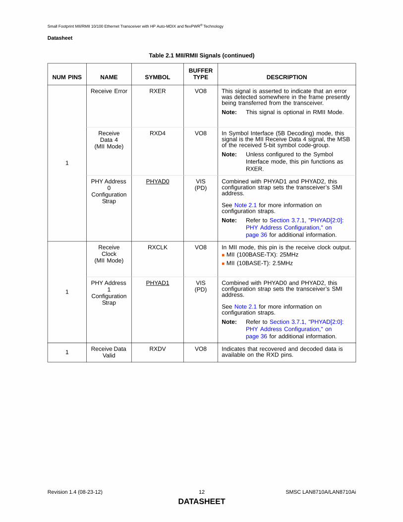
1
Receive Error RXER VO8 This signal is asserted to indicate that an error was detected somewhere in the frame presently being transferred from the transceiver. Note: This signal is optional in RMII Mode.
Receive Data 4
(MII Mode)
RXD4 VO8 In Symbol Interface (5B Decoding) mode, this signal is the MII Receive Data 4 signal, the MSB of the received 5-bit symbol code-group. Note: Unless configured to the Symbol
Interface mode, this pin functions as RXER.
PHY Address 0
Configuration Strap
PHYAD0 VIS(PD)
Combined with PHYAD1 and PHYAD2, this configuration strap sets the transceiver’s SMI address.
See Note 2.1 for more information on configuration straps. Note: Refer to Section 3.7.1, "PHYAD[2:0]:
PHY Address Configuration," on page 36 for additional information.
1
Receive Clock
(MII Mode)
RXCLK VO8 In MII mode, this pin is the receive clock output.MII (100BASE-TX): 25MHzMII (10BASE-T): 2.5MHz
PHY Address 1
Configuration Strap
PHYAD1 VIS(PD)
Combined with PHYAD0 and PHYAD2, this configuration strap sets the transceiver’s SMI address.
See Note 2.1 for more information on configuration straps. Note: Refer to Section 3.7.1, "PHYAD[2:0]:
PHY Address Configuration," on page 36 for additional information.
1 Receive Data Valid
RXDV VO8 Indicates that recovered and decoded data is available on the RXD pins.
Table 2.1 MII/RMII Signals (continued)
NUM PINS NAME SYMBOLBUFFER
TYPE DESCRIPTION
Revision 1.4 (08-23-12) 12 SMSC LAN8710A/LAN8710Ai
DATASHEET

Small Footprint MII/RMII 10/100 Ethernet Transceiver with HP Auto-MDIX and flexPWR® Technology
Datasheet
Note 2.1 Configuration strap values are latched on power-on reset and system reset. Configurationstraps are identified by an underlined symbol name. Signals that function as configurationstraps must be augmented with an external resistor when connected to a load. Refer toSection 3.7, "Configuration Straps," on page 36 for additional information.
1
Carrier Sense / Receive Data Valid
(RMII Mode)
CRS_DV VO8 This signal is asserted to indicate the receive medium is non-idle in RMII Mode. When a 10BASE-T packet is received, CRS_DV is asserted, but RXD[1:0] is held low until the SFD byte (10101011) is received. Note: Per the RMII standard, transmitted data
is not looped back onto the receive data pins in 10BASE-T half-duplex mode.
Collision Detect
(MII Mode)
COL VO8 This signal is asserted to indicate detection of a collision condition in MII Mode.
PHY Operating Mode 2
Configuration Strap
MODE2 VIS(PU)
Combined with MODE0 and MODE1, this configuration strap sets the default PHY mode.
See Note 2.1 for more information on configuration straps. Note: Refer to Section 3.7.2, "MODE[2:0]:
Mode Configuration," on page 36 for additional details.
1 Carrier Sense(MII Mode)
CRS VO8(PD)
This signal indicates detection of a carrier in MII Mode.
Table 2.2 LED Pins
NUM PINS NAME SYMBOLBUFFER
TYPE DESCRIPTION
1
LED 1 LED1 O12 Link activity LED Indication. This pin is driven active when a valid link is detected and blinks when activity is detected.Note: Refer to Section 3.8.1, "LEDs," on
page 39 for additional LED information.
Regulator Off Configuration
Strap
REGOFF IS(PD)
This configuration strap is used to disable the internal 1.2V regulator. When the regulator is disabled, external 1.2V must be supplied to VDDCR.
When REGOFF is pulled high to VDD2A with an external resistor, the internal regulator is disabled. When REGOFF is floating or pulled low, the internal regulator is enabled (default).
See Note 2.2 for more information on configuration straps. Note: Refer to Section 3.7.4, "REGOFF:
Internal +1.2V Regulator Configuration," on page 38 for additional details.
Table 2.1 MII/RMII Signals (continued)
NUM PINS NAME SYMBOLBUFFER
TYPE DESCRIPTION
SMSC LAN8710A/LAN8710Ai 13 Revision 1.4 (08-23-12)
DATASHEET
Small Footprint MII/RMII 10/100 Ethernet Transceiver with HP Auto-MDIX and flexPWR® Technology
Datasheet
Note 2.2 Configuration strap values are latched on power-on reset and system reset. Configurationstraps are identified by an underlined symbol name. Signals that function as configurationstraps must be augmented with an external resistor when connected to a load. Refer toSection 3.7, "Configuration Straps," on page 36 for additional information.
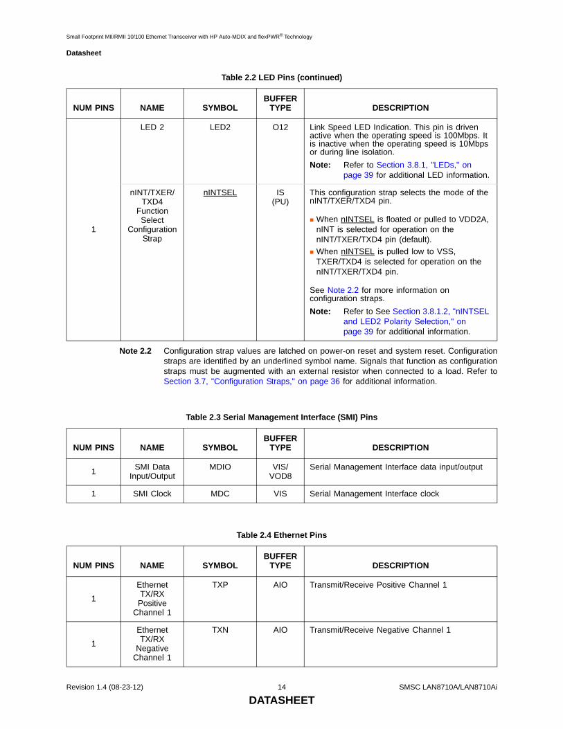
1
LED 2 LED2 O12 Link Speed LED Indication. This pin is driven active when the operating speed is 100Mbps. It is inactive when the operating speed is 10Mbps or during line isolation.Note: Refer to Section 3.8.1, "LEDs," on
page 39 for additional LED information.
nINT/TXER/TXD4
Function Select
Configuration Strap
nINTSEL IS(PU)
This configuration strap selects the mode of the nINT/TXER/TXD4 pin.
When nINTSEL is floated or pulled to VDD2A, nINT is selected for operation on the nINT/TXER/TXD4 pin (default).When nINTSEL is pulled low to VSS, TXER/TXD4 is selected for operation on the nINT/TXER/TXD4 pin.
See Note 2.2 for more information on configuration straps. Note: Refer to See Section 3.8.1.2, "nINTSEL
and LED2 Polarity Selection," on page 39 for additional information.
Table 2.3 Serial Management Interface (SMI) Pins
NUM PINS NAME SYMBOLBUFFER
TYPE DESCRIPTION
1 SMI Data Input/Output
MDIO VIS/VOD8
Serial Management Interface data input/output
1 SMI Clock MDC VIS Serial Management Interface clock
Table 2.4 Ethernet Pins
NUM PINS NAME SYMBOLBUFFER
TYPE DESCRIPTION
1
Ethernet TX/RX Positive
Channel 1
TXP AIO Transmit/Receive Positive Channel 1
1
Ethernet TX/RX
Negative Channel 1
TXN AIO Transmit/Receive Negative Channel 1
Table 2.2 LED Pins (continued)
NUM PINS NAME SYMBOLBUFFER
TYPE DESCRIPTION
Revision 1.4 (08-23-12) 14 SMSC LAN8710A/LAN8710Ai
DATASHEET
Small Footprint MII/RMII 10/100 Ethernet Transceiver with HP Auto-MDIX and flexPWR® Technology
Datasheet
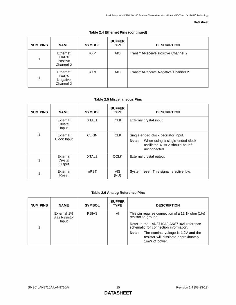
1
Ethernet TX/RX Positive
Channel 2
RXP AIO Transmit/Receive Positive Channel 2
1
Ethernet TX/RX
Negative Channel 2
RXN AIO Transmit/Receive Negative Channel 2
Table 2.5 Miscellaneous Pins
NUM PINS NAME SYMBOLBUFFER
TYPE DESCRIPTION
1
External Crystal Input
XTAL1 ICLK External crystal input
External Clock Input
CLKIN ICLK Single-ended clock oscillator input.Note: When using a single ended clock
oscillator, XTAL2 should be left unconnected.
1External Crystal Output
XTAL2 OCLK External crystal output
1 External Reset
nRST VIS(PU)
System reset. This signal is active low.
Table 2.6 Analog Reference Pins
NUM PINS NAME SYMBOLBUFFER
TYPE DESCRIPTION
1
External 1% Bias Resistor
Input
RBIAS AI This pin requires connection of a 12.1k ohm (1%) resistor to ground.
Refer to the LAN8710A/LAN8710Ai reference schematic for connection information.Note: The nominal voltage is 1.2V and the
resistor will dissipate approximately 1mW of power.
Table 2.4 Ethernet Pins (continued)
NUM PINS NAME SYMBOLBUFFER
TYPE DESCRIPTION
SMSC LAN8710A/LAN8710Ai 15 Revision 1.4 (08-23-12)
DATASHEET
Small Footprint MII/RMII 10/100 Ethernet Transceiver with HP Auto-MDIX and flexPWR® Technology
Datasheet
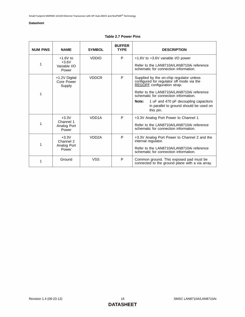
Table 2.7 Power Pins
NUM PINS NAME SYMBOLBUFFER
TYPE DESCRIPTION
1
+1.6V to +3.6V
Variable I/O Power
VDDIO P +1.6V to +3.6V variable I/O power
Refer to the LAN8710A/LAN8710Ai reference schematic for connection information.
1
+1.2V Digital Core Power
Supply
VDDCR P Supplied by the on-chip regulator unless configured for regulator off mode via the REGOFF configuration strap.
Refer to the LAN8710A/LAN8710Ai reference schematic for connection information.Note: 1 uF and 470 pF decoupling capacitors
in parallel to ground should be used on this pin.
1
+3.3V Channel 1
Analog Port Power
VDD1A P +3.3V Analog Port Power to Channel 1
Refer to the LAN8710A/LAN8710Ai reference schematic for connection information.
1
+3.3V Channel 2
Analog Port Power
VDD2A P +3.3V Analog Port Power to Channel 2 and the internal regulator.
Refer to the LAN8710A/LAN8710Ai reference schematic for connection information.
1 Ground VSS P Common ground. This exposed pad must be connected to the ground plane with a via array.
Revision 1.4 (08-23-12) 16 SMSC LAN8710A/LAN8710Ai
DATASHEET
Small Footprint MII/RMII 10/100 Ethernet Transceiver with HP Auto-MDIX and flexPWR® Technology
Datasheet
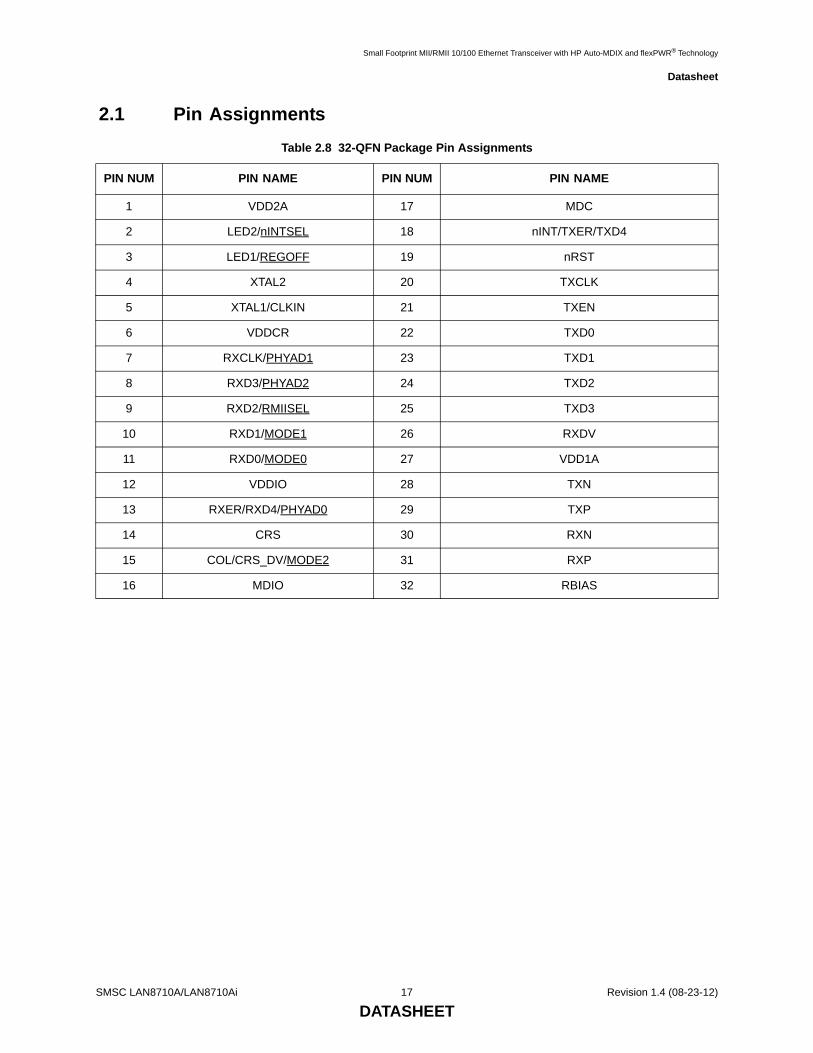
2.1 Pin AssignmentsTable 2.8 32-QFN Package Pin Assignments
PIN NUM PIN NAME PIN NUM PIN NAME
1 VDD2A 17 MDC
2 LED2/nINTSEL 18 nINT/TXER/TXD4
3 LED1/REGOFF 19 nRST
4 XTAL2 20 TXCLK
5 XTAL1/CLKIN 21 TXEN
6 VDDCR 22 TXD0
7 RXCLK/PHYAD1 23 TXD1
8 RXD3/PHYAD2 24 TXD2
9 RXD2/RMIISEL 25 TXD3
10 RXD1/MODE1 26 RXDV
11 RXD0/MODE0 27 VDD1A
12 VDDIO 28 TXN
13 RXER/RXD4/PHYAD0 29 TXP
14 CRS 30 RXN
15 COL/CRS_DV/MODE2 31 RXP
16 MDIO 32 RBIAS
SMSC LAN8710A/LAN8710Ai 17 Revision 1.4 (08-23-12)
DATASHEET
Small Footprint MII/RMII 10/100 Ethernet Transceiver with HP Auto-MDIX and flexPWR® Technology
Datasheet
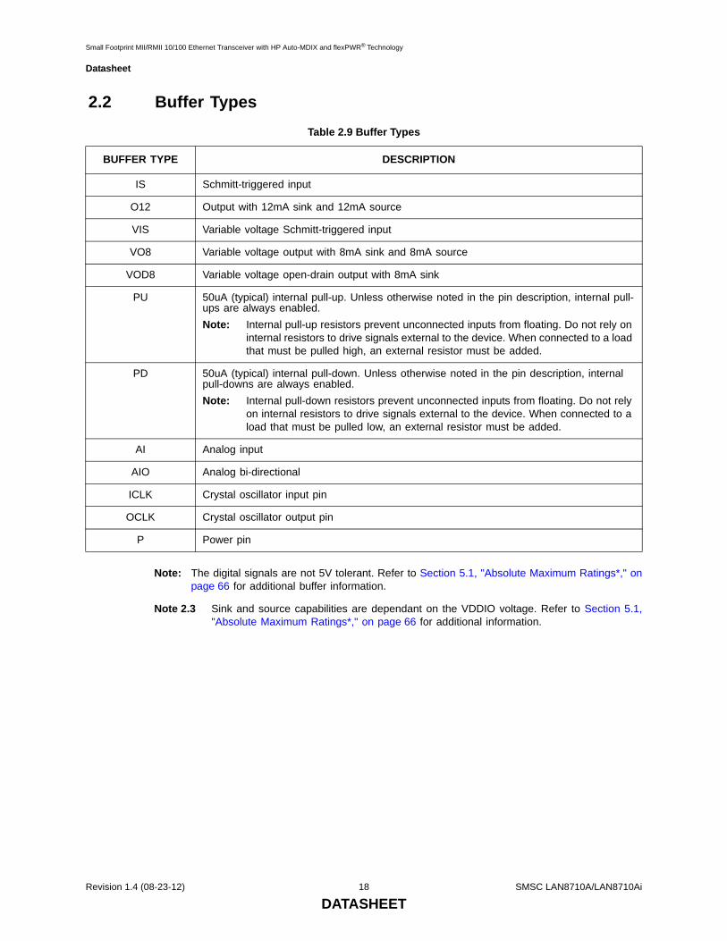
2.2 Buffer Types
Note: The digital signals are not 5V tolerant. Refer to Section 5.1, "Absolute Maximum Ratings*," onpage 66 for additional buffer information.
Note 2.3 Sink and source capabilities are dependant on the VDDIO voltage. Refer to Section 5.1,"Absolute Maximum Ratings*," on page 66 for additional information.
Table 2.9 Buffer Types
BUFFER TYPE DESCRIPTION
IS Schmitt-triggered input
O12 Output with 12mA sink and 12mA source
VIS Variable voltage Schmitt-triggered input
VO8 Variable voltage output with 8mA sink and 8mA source
VOD8 Variable voltage open-drain output with 8mA sink
PU 50uA (typical) internal pull-up. Unless otherwise noted in the pin description, internal pull-ups are always enabled. Note: Internal pull-up resistors prevent unconnected inputs from floating. Do not rely on
internal resistors to drive signals external to the device. When connected to a load that must be pulled high, an external resistor must be added.
PD 50uA (typical) internal pull-down. Unless otherwise noted in the pin description, internal pull-downs are always enabled.Note: Internal pull-down resistors prevent unconnected inputs from floating. Do not rely
on internal resistors to drive signals external to the device. When connected to a load that must be pulled low, an external resistor must be added.
AI Analog input
AIO Analog bi-directional
ICLK Crystal oscillator input pin
OCLK Crystal oscillator output pin
P Power pin
Revision 1.4 (08-23-12) 18 SMSC LAN8710A/LAN8710Ai
DATASHEET

Small Footprint MII/RMII 10/100 Ethernet Transceiver with HP Auto-MDIX and flexPWR® Technology
Datasheet
Chapter 3 Functional Description
This chapter provides functional descriptions of the various device features. These features have beencategorized into the following sections:
Transceiver
Auto-negotiation
HP Auto-MDIX Support
MAC Interface
Serial Management Interface (SMI)
Interrupt Management
Configuration Straps
Miscellaneous Functions
Application Diagrams
3.1 Transceiver
3.1.1 100BASE-TX Transmit
The 100BASE-TX transmit data path is shown in Figure 3.1. Each major block is explained in thefollowing subsections.
3.1.1.1 100BASE-TX Transmit Data Across the MII/RMII Interface
For MII, the MAC controller drives the transmit data onto the TXD bus and asserts TXEN to indicatevalid data. The data is latched by the transceiver’s MII block on the rising edge of TXCLK. The datais in the form of 4-bit wide 25MHz data.
Figure 3.1 100BASE-TX Transmit Data Path
MAC
Tx Driver
MLT-3 Converter
NRZI Converter
4B/5B Encoder
CAT-5RJ45
25MHz by5 bits
NRZI
MLT-3MLT-3
MLT-3
Scrambler and PISOMII/RMII 25MHz
by 4 bits
Ext Ref_CLK (for RMII only)
PLL
MII 25 Mhz by 4 bitsor
RMII 50Mhz by 2 bits
MLT-3Magnetics
125 Mbps Serial
TX_CLK(for MII only)
SMSC LAN8710A/LAN8710Ai 19 Revision 1.4 (08-23-12)
DATASHEET
Small Footprint MII/RMII 10/100 Ethernet Transceiver with HP Auto-MDIX and flexPWR® Technology
Datasheet
For RMII, the MAC controller drives the transmit data onto the TXD bus and asserts TXEN to indicatevalid data. The data is latched by the transceiver’s RMII block on the rising edge of REF_CLK. Thedata is in the form of 2-bit wide 50MHz data.
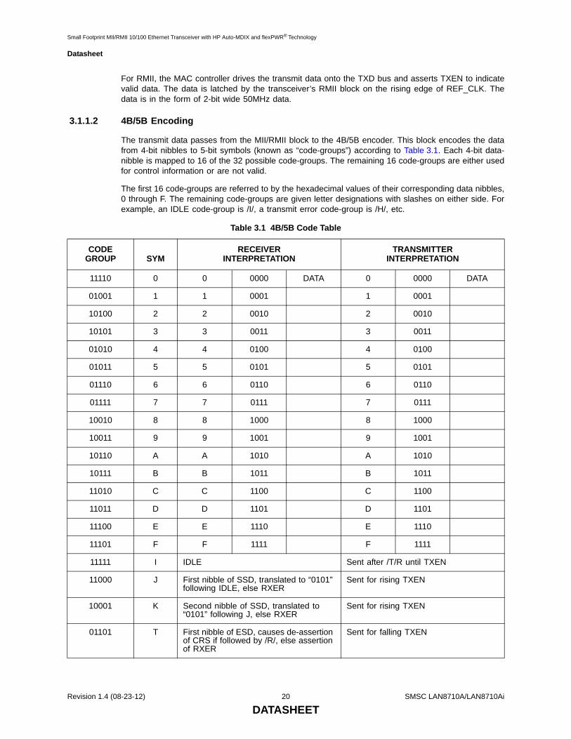
3.1.1.2 4B/5B Encoding
The transmit data passes from the MII/RMII block to the 4B/5B encoder. This block encodes the datafrom 4-bit nibbles to 5-bit symbols (known as “code-groups”) according to Table 3.1. Each 4-bit data-nibble is mapped to 16 of the 32 possible code-groups. The remaining 16 code-groups are either usedfor control information or are not valid.
The first 16 code-groups are referred to by the hexadecimal values of their corresponding data nibbles,0 through F. The remaining code-groups are given letter designations with slashes on either side. Forexample, an IDLE code-group is /I/, a transmit error code-group is /H/, etc.
Table 3.1 4B/5B Code Table
CODEGROUP SYM
RECEIVERINTERPRETATION
TRANSMITTERINTERPRETATION
11110 0 0 0000 DATA 0 0000 DATA
01001 1 1 0001 1 0001
10100 2 2 0010 2 0010
10101 3 3 0011 3 0011
01010 4 4 0100 4 0100
01011 5 5 0101 5 0101
01110 6 6 0110 6 0110
01111 7 7 0111 7 0111
10010 8 8 1000 8 1000
10011 9 9 1001 9 1001
10110 A A 1010 A 1010
10111 B B 1011 B 1011
11010 C C 1100 C 1100
11011 D D 1101 D 1101
11100 E E 1110 E 1110
11101 F F 1111 F 1111
11111 I IDLE Sent after /T/R until TXEN
11000 J First nibble of SSD, translated to “0101” following IDLE, else RXER
Sent for rising TXEN
10001 K Second nibble of SSD, translated to “0101” following J, else RXER
Sent for rising TXEN
01101 T First nibble of ESD, causes de-assertion of CRS if followed by /R/, else assertion of RXER
Sent for falling TXEN
Revision 1.4 (08-23-12) 20 SMSC LAN8710A/LAN8710Ai
DATASHEET
Small Footprint MII/RMII 10/100 Ethernet Transceiver with HP Auto-MDIX and flexPWR® Technology
Datasheet
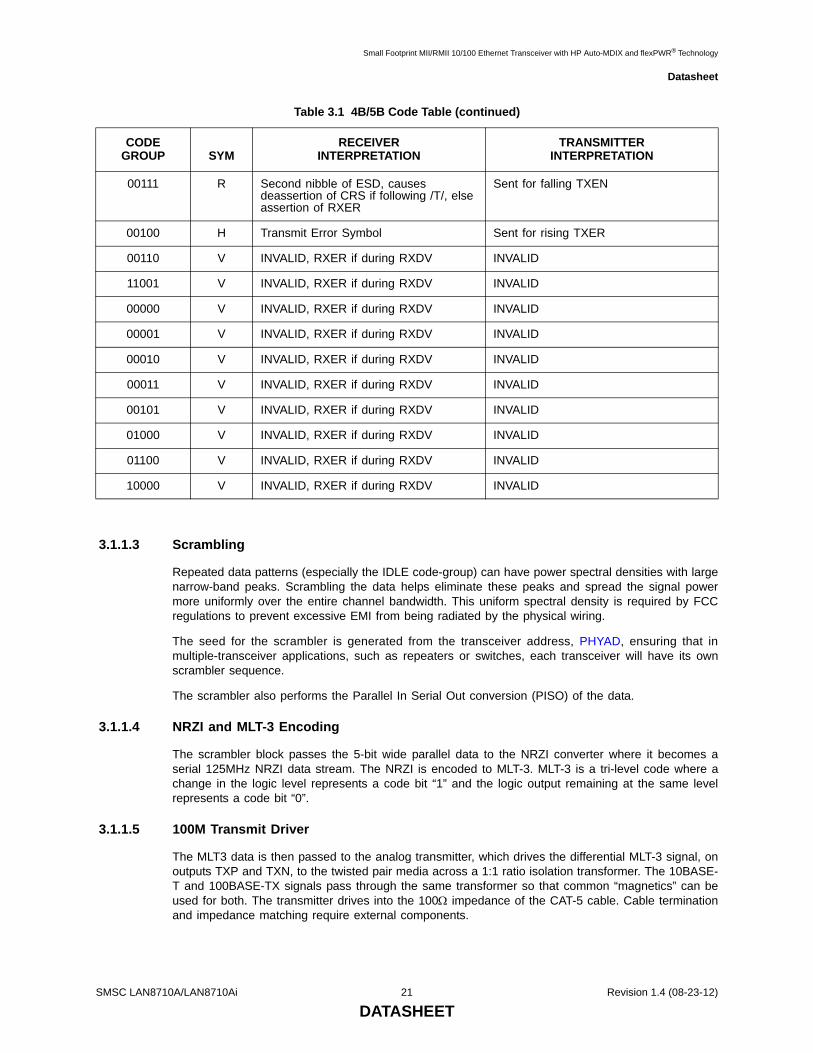
3.1.1.3 Scrambling
Repeated data patterns (especially the IDLE code-group) can have power spectral densities with largenarrow-band peaks. Scrambling the data helps eliminate these peaks and spread the signal powermore uniformly over the entire channel bandwidth. This uniform spectral density is required by FCCregulations to prevent excessive EMI from being radiated by the physical wiring.
The seed for the scrambler is generated from the transceiver address, PHYAD, ensuring that inmultiple-transceiver applications, such as repeaters or switches, each transceiver will have its ownscrambler sequence.
The scrambler also performs the Parallel In Serial Out conversion (PISO) of the data.
3.1.1.4 NRZI and MLT-3 Encoding
The scrambler block passes the 5-bit wide parallel data to the NRZI converter where it becomes aserial 125MHz NRZI data stream. The NRZI is encoded to MLT-3. MLT-3 is a tri-level code where achange in the logic level represents a code bit “1” and the logic output remaining at the same levelrepresents a code bit “0”.
3.1.1.5 100M Transmit Driver
The MLT3 data is then passed to the analog transmitter, which drives the differential MLT-3 signal, onoutputs TXP and TXN, to the twisted pair media across a 1:1 ratio isolation transformer. The 10BASE-T and 100BASE-TX signals pass through the same transformer so that common “magnetics” can beused for both. The transmitter drives into the 100Ω impedance of the CAT-5 cable. Cable terminationand impedance matching require external components.
00111 R Second nibble of ESD, causes deassertion of CRS if following /T/, else assertion of RXER
Sent for falling TXEN
00100 H Transmit Error Symbol Sent for rising TXER
00110 V INVALID, RXER if during RXDV INVALID
11001 V INVALID, RXER if during RXDV INVALID
00000 V INVALID, RXER if during RXDV INVALID
00001 V INVALID, RXER if during RXDV INVALID
00010 V INVALID, RXER if during RXDV INVALID
00011 V INVALID, RXER if during RXDV INVALID
00101 V INVALID, RXER if during RXDV INVALID
01000 V INVALID, RXER if during RXDV INVALID
01100 V INVALID, RXER if during RXDV INVALID
10000 V INVALID, RXER if during RXDV INVALID
Table 3.1 4B/5B Code Table (continued)
CODEGROUP SYM
RECEIVERINTERPRETATION
TRANSMITTERINTERPRETATION
SMSC LAN8710A/LAN8710Ai 21 Revision 1.4 (08-23-12)
DATASHEET

Small Footprint MII/RMII 10/100 Ethernet Transceiver with HP Auto-MDIX and flexPWR® Technology
Datasheet
3.1.1.6 100M Phase Lock Loop (PLL)
The 100M PLL locks onto reference clock and generates the 125MHz clock used to drive the 125 MHzlogic and the 100BASE-TX transmitter.
3.1.2 100BASE-TX Receive
The 100BASE-TX receive data path is shown in Figure 3.2. Each major block is explained in thefollowing subsections.
3.1.2.1 100M Receive Input
The MLT-3 from the cable is fed into the transceiver (on inputs RXP and RXN) via a 1:1 ratiotransformer. The ADC samples the incoming differential signal at a rate of 125M samples per second.Using a 64-level quanitizer, it generates 6 digital bits to represent each sample. The DSP adjusts thegain of the ADC according to the observed signal levels such that the full dynamic range of the ADCcan be used.
3.1.2.2 Equalizer, Baseline Wander Correction and Clock and Data Recovery
The 6 bits from the ADC are fed into the DSP block. The equalizer in the DSP section compensatesfor phase and amplitude distortion caused by the physical channel consisting of magnetics, connectors,and CAT- 5 cable. The equalizer can restore the signal for any good-quality CAT-5 cable between 1mand 150m.
If the DC content of the signal is such that the low-frequency components fall below the low frequencypole of the isolation transformer, then the droop characteristics of the transformer will becomesignificant and Baseline Wander (BLW) on the received signal will result. To prevent corruption of thereceived data, the transceiver corrects for BLW and can receive the ANSI X3.263-1995 FDDI TP-PMDdefined “killer packet” with no bit errors.
Figure 3.2 100BASE-TX Receive Data Path
MAC
A/D Converter
MLT-3 Converter
NRZI Converter
4B/5B Decoder
Magnetics CAT-5RJ45
PLL
MII 25Mhz by 4 bitsor
RMII 50Mhz by 2 bits
RX_CLK(for MII only)
25MHz by5 bits
NRZI
MLT-3MLT-3 MLT-3
6 bit Data
Descrambler and SIPO
125 Mbps Serial
DSP: Timing recovery, Equalizer and BLW Correction
MLT-3
MII/RMII25MHz
by 4 bits
Ext Ref_CLK (for RMII only)
Revision 1.4 (08-23-12) 22 SMSC LAN8710A/LAN8710Ai
DATASHEET

Small Footprint MII/RMII 10/100 Ethernet Transceiver with HP Auto-MDIX and flexPWR® Technology
Datasheet
The 100M PLL generates multiple phases of the 125MHz clock. A multiplexer, controlled by the timingunit of the DSP, selects the optimum phase for sampling the data. This is used as the receivedrecovered clock. This clock is used to extract the serial data from the received signal.
3.1.2.3 NRZI and MLT-3 Decoding
The DSP generates the MLT-3 recovered levels that are fed to the MLT-3 converter. The MLT-3 is thenconverted to an NRZI data stream.
3.1.2.4 Descrambling
The descrambler performs an inverse function to the scrambler in the transmitter and also performsthe Serial In Parallel Out (SIPO) conversion of the data.
During reception of IDLE (/I/) symbols. the descrambler synchronizes its descrambler key to theincoming stream. Once synchronization is achieved, the descrambler locks on this key and is able todescramble incoming data.
Special logic in the descrambler ensures synchronization with the remote transceiver by searching forIDLE symbols within a window of 4000 bytes (40us). This window ensures that a maximum packet sizeof 1514 bytes, allowed by the IEEE 802.3 standard, can be received with no interference. If no IDLE-symbols are detected within this time-period, receive operation is aborted and the descrambler re-startsthe synchronization process.
3.1.2.5 Alignment
The de-scrambled signal is then aligned into 5-bit code-groups by recognizing the /J/K/ Start-of-StreamDelimiter (SSD) pair at the start of a packet. Once the code-word alignment is determined, it is storedand utilized until the next start of frame.
3.1.2.6 5B/4B Decoding
The 5-bit code-groups are translated into 4-bit data nibbles according to the 4B/5B table. Thetranslated data is presented on the RXD[3:0] signal lines. The SSD, /J/K/, is translated to “0101 0101”as the first 2 nibbles of the MAC preamble. Reception of the SSD causes the transceiver to assert thereceive data valid signal, indicating that valid data is available on the RXD bus. Successive valid code-groups are translated to data nibbles. Reception of either the End of Stream Delimiter (ESD) consistingof the /T/R/ symbols, or at least two /I/ symbols causes the transceiver to de-assert the carrier senseand receive data valid signals.
Note: These symbols are not translated into data.
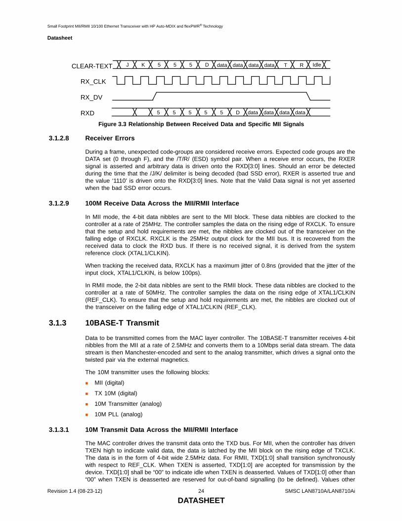
3.1.2.7 Receive Data Valid Signal
The Receive Data Valid signal (RXDV) indicates that recovered and decoded nibbles are beingpresented on the RXD[3:0] outputs synchronous to RXCLK. RXDV becomes active after the /J/K/delimiter has been recognized and RXD is aligned to nibble boundaries. It remains active until eitherthe /T/R/ delimiter is recognized or link test indicates failure or SIGDET becomes false.
RXDV is asserted when the first nibble of translated /J/K/ is ready for transfer over the MediaIndependent Interface (MII mode).
SMSC LAN8710A/LAN8710Ai 23 Revision 1.4 (08-23-12)
DATASHEET
Small Footprint MII/RMII 10/100 Ethernet Transceiver with HP Auto-MDIX and flexPWR® Technology
Datasheet
Figure 3.3 Relationship Between Received Data and Specific MII Signals
3.1.2.8 Receiver Errors
During a frame, unexpected code-groups are considered receive errors. Expected code groups are theDATA set (0 through F), and the /T/R/ (ESD) symbol pair. When a receive error occurs, the RXERsignal is asserted and arbitrary data is driven onto the RXD[3:0] lines. Should an error be detectedduring the time that the /J/K/ delimiter is being decoded (bad SSD error), RXER is asserted true andthe value ‘1110’ is driven onto the RXD[3:0] lines. Note that the Valid Data signal is not yet assertedwhen the bad SSD error occurs.
3.1.2.9 100M Receive Data Across the MII/RMII Interface
In MII mode, the 4-bit data nibbles are sent to the MII block. These data nibbles are clocked to thecontroller at a rate of 25MHz. The controller samples the data on the rising edge of RXCLK. To ensurethat the setup and hold requirements are met, the nibbles are clocked out of the transceiver on thefalling edge of RXCLK. RXCLK is the 25MHz output clock for the MII bus. It is recovered from thereceived data to clock the RXD bus. If there is no received signal, it is derived from the systemreference clock (XTAL1/CLKIN).
When tracking the received data, RXCLK has a maximum jitter of 0.8ns (provided that the jitter of theinput clock, XTAL1/CLKIN, is below 100ps).
In RMII mode, the 2-bit data nibbles are sent to the RMII block. These data nibbles are clocked to thecontroller at a rate of 50MHz. The controller samples the data on the rising edge of XTAL1/CLKIN(REF_CLK). To ensure that the setup and hold requirements are met, the nibbles are clocked out ofthe transceiver on the falling edge of XTAL1/CLKIN (REF_CLK).
3.1.3 10BASE-T Transmit
Data to be transmitted comes from the MAC layer controller. The 10BASE-T transmitter receives 4-bitnibbles from the MII at a rate of 2.5MHz and converts them to a 10Mbps serial data stream. The datastream is then Manchester-encoded and sent to the analog transmitter, which drives a signal onto thetwisted pair via the external magnetics.
The 10M transmitter uses the following blocks:
MII (digital)
TX 10M (digital)
10M Transmitter (analog)
10M PLL (analog)
3.1.3.1 10M Transmit Data Across the MII/RMII Interface
The MAC controller drives the transmit data onto the TXD bus. For MII, when the controller has drivenTXEN high to indicate valid data, the data is latched by the MII block on the rising edge of TXCLK.The data is in the form of 4-bit wide 2.5MHz data. For RMII, TXD[1:0] shall transition synchronouslywith respect to REF_CLK. When TXEN is asserted, TXD[1:0] are accepted for transmission by thedevice. TXD[1:0] shall be “00” to indicate idle when TXEN is deasserted. Values of TXD[1:0] other than“00” when TXEN is deasserted are reserved for out-of-band signalling (to be defined). Values other
5 D5 data data data dataRXD
RX_DV
RX_CLK
5 D5 data data data dataCLEAR-TEXT 5J K
5 5 5
T R Idle
Revision 1.4 (08-23-12) 24 SMSC LAN8710A/LAN8710Ai
DATASHEET

Small Footprint MII/RMII 10/100 Ethernet Transceiver with HP Auto-MDIX and flexPWR® Technology
Datasheet
than “00” on TXD[1:0] while TXEN is deasserted shall be ignored by the device.TXD[1:0] shall providevalid data for each REF_CLK period while TXEN is asserted.
In order to comply with legacy 10BASE-T MAC/Controllers, in half-duplex mode the transceiver loopsback the transmitted data, on the receive path. This does not confuse the MAC/Controller since theCOL signal is not asserted during this time. The transceiver also supports the SQE (Heartbeat) signal.See Section 3.8.7, "Collision Detect," on page 42, for more details.
3.1.3.2 Manchester Encoding
The 4-bit wide data is sent to the 10M TX block. The nibbles are converted to a 10Mbps serial NRZIdata stream. The 10M PLL locks onto the external clock or internal oscillator and produces a 20MHzclock. This is used to Manchester encode the NRZ data stream. When no data is being transmitted(TXEN is low), the 10M TX block outputs Normal Link Pulses (NLPs) to maintain communications withthe remote link partner.
3.1.3.3 10M Transmit Drivers
The Manchester encoded data is sent to the analog transmitter where it is shaped and filtered beforebeing driven out as a differential signal across the TXP and TXN outputs.
3.1.4 10BASE-T Receive
The 10BASE-T receiver gets the Manchester- encoded analog signal from the cable via the magnetics.It recovers the receive clock from the signal and uses this clock to recover the NRZI data stream. This10M serial data is converted to 4-bit data nibbles which are passed to the controller via MII at a rateof 2.5MHz.
This 10M receiver uses the following blocks:
Filter and SQUELCH (analog)
10M PLL (analog)
RX 10M (digital)
MII (digital)
3.1.4.1 10M Receive Input and Squelch
The Manchester signal from the cable is fed into the transceiver (on inputs RXP and RXN) via 1:1 ratiomagnetics. It is first filtered to reduce any out-of-band noise. It then passes through a SQUELCHcircuit. The SQUELCH is a set of amplitude and timing comparators that normally reject differentialvoltage levels below 300mV and detect and recognize differential voltages above 585mV.
3.1.4.2 Manchester Decoding
The output of the SQUELCH goes to the 10M RX block where it is validated as Manchester encodeddata. The polarity of the signal is also checked. If the polarity is reversed (local RXP is connected toRXN of the remote partner and vice versa), the condition is identified and corrected. The reversedcondition is indicated by the XPOL bit of the Special Control/Status Indications Register. The 10M PLLis locked onto the received Manchester signal, from which the 20MHz cock is generated. Using thisclock, the Manchester encoded data is extracted and converted to a 10MHz NRZI data stream. It isthen converted from serial to 4-bit wide parallel data.
The 10M RX block also detects valid 10Base-T IDLE signals - Normal Link Pulses (NLPs) - to maintainthe link.
SMSC LAN8710A/LAN8710Ai 25 Revision 1.4 (08-23-12)
DATASHEET

Small Footprint MII/RMII 10/100 Ethernet Transceiver with HP Auto-MDIX and flexPWR® Technology
Datasheet
3.1.4.3 10M Receive Data Across the MII/RMII Interface
For MII, the 4-bit data nibbles are sent to the MII block. In MII mode, these data nibbles are valid onthe rising edge of the 2.5 MHz RXCLK.
For RMII, the 2-bit data nibbles are sent to the RMII block. In RMII mode, these data nibbles are validon the rising edge of the RMII REF_CLK.
3.1.4.4 Jabber Detection
Jabber is a condition in which a station transmits for a period of time longer than the maximumpermissible packet length, usually due to a fault condition, which results in holding the TXEN input fora long period. Special logic is used to detect the jabber state and abort the transmission to the linewithin 45ms. Once TXEN is deasserted, the logic resets the jabber condition.
As shown in Section 4.2.2, "Basic Status Register," on page 53, the Jabber Detect bit indicates that ajabber condition was detected.
3.2 Auto-negotiationThe purpose of the auto-negotiation function is to automatically configure the transceiver to theoptimum link parameters based on the capabilities of its link partner. Auto-negotiation is a mechanismfor exchanging configuration information between two link-partners and automatically selecting thehighest performance mode of operation supported by both sides. Auto-negotiation is fully defined inclause 28 of the IEEE 802.3 specification.
Once auto-negotiation has completed, information about the resolved link can be passed back to thecontroller via the Serial Management Interface (SMI). The results of the negotiation process arereflected in the Speed Indication bits of the PHY Special Control/Status Register, as well as in the AutoNegotiation Link Partner Ability Register. The auto-negotiation protocol is a purely physical layeractivity and proceeds independently of the MAC controller.
The advertised capabilities of the transceiver are stored in the Auto Negotiation AdvertisementRegister. The default advertised by the transceiver is determined by user-defined on-chip signaloptions.
The following blocks are activated during an Auto-negotiation session:
Auto-negotiation (digital)
100M ADC (analog)
100M PLL (analog)
100M equalizer/BLW/clock recovery (DSP)
10M SQUELCH (analog)
10M PLL (analog)
10M Transmitter (analog)
When enabled, auto-negotiation is started by the occurrence of one of the following events:
Hardware reset
Software reset
Power-down reset
Link status down
Setting the Restart Auto-Negotiate bit of the Basic Control Register
On detection of one of these events, the transceiver begins auto-negotiation by transmitting bursts ofFast Link Pulses (FLP), which are bursts of link pulses from the 10M transmitter. They are shaped asNormal Link Pulses and can pass uncorrupted down CAT-3 or CAT-5 cable. A Fast Link Pulse Burst
Revision 1.4 (08-23-12) 26 SMSC LAN8710A/LAN8710Ai
DATASHEET

Small Footprint MII/RMII 10/100 Ethernet Transceiver with HP Auto-MDIX and flexPWR® Technology
Datasheet
consists of up to 33 pulses. The 17 odd-numbered pulses, which are always present, frame the FLPburst. The 16 even-numbered pulses, which may be present or absent, contain the data word beingtransmitted. Presence of a data pulse represents a “1”, while absence represents a “0”.
The data transmitted by an FLP burst is known as a “Link Code Word.” These are defined fully in IEEE802.3 clause 28. In summary, the transceiver advertises 802.3 compliance in its selector field (the first5 bits of the Link Code Word). It advertises its technology ability according to the bits set in the AutoNegotiation Advertisement Register.
There are 4 possible matches of the technology abilities. In the order of priority these are:
100M Full Duplex (Highest Priority)
100M Half Duplex
10M Full Duplex
10M Half Duplex (Lowest Priority)
If the full capabilities of the transceiver are advertised (100M, Full Duplex), and if the link partner iscapable of 10M and 100M, then auto-negotiation selects 100M as the highest performance mode. Ifthe link partner is capable of half and full duplex modes, then auto-negotiation selects full duplex asthe highest performance operation.
Once a capability match has been determined, the link code words are repeated with the acknowledgebit set. Any difference in the main content of the link code words at this time will cause auto-negotiationto re-start. Auto-negotiation will also re-start if not all of the required FLP bursts are received.
The capabilities advertised during auto-negotiation by the transceiver are initially determined by thelogic levels latched on the MODE[2:0] configuration straps after reset completes. These configurationstraps can also be used to disable auto-negotiation on power-up. Refer to Section 3.7.2, "MODE[2:0]:Mode Configuration," on page 36 for additional information.
Writing the bits 8 through 5 of the Auto Negotiation Advertisement Register allows software control ofthe capabilities advertised by the transceiver. Writing the Auto Negotiation Advertisement Registerdoes not automatically re-start auto-negotiation. The Restart Auto-Negotiate bit of the Basic ControlRegister must be set before the new abilities will be advertised. Auto-negotiation can also be disabledvia software by clearing the Auto-Negotiation Enable bit of the Basic Control Register.
Note: The device does not support “Next Page” capability.
3.2.1 Parallel Detection
If the LAN8710A/LAN8710Ai is connected to a device lacking the ability to auto-negotiate (i.e. no FLPsare detected), it is able to determine the speed of the link based on either 100M MLT-3 symbols or10M Normal Link Pulses. In this case the link is presumed to be half duplex per the IEEE standard.This ability is known as “Parallel Detection.” This feature ensures interoperability with legacy linkpartners. If a link is formed via parallel detection, then the Link Partner Auto-Negotiation Able bit of theAuto Negotiation Expansion Register is cleared to indicate that the Link Partner is not capable of auto-negotiation. The controller has access to this information via the management interface. If a faultoccurs during parallel detection, the Parallel Detection Fault bit of Link Partner Auto-Negotiation Ableis set.
Auto Negotiation Link Partner Ability Register is used to store the link partner ability information, whichis coded in the received FLPs. If the link partner is not auto-negotiation capable, then the AutoNegotiation Link Partner Ability Register is updated after completion of parallel detection to reflect thespeed capability of the link partner.
3.2.2 Restarting Auto-negotiation
Auto-negotiation can be restarted at any time by setting the Restart Auto-Negotiate bit of the BasicControl Register. Auto-negotiation will also restart if the link is broken at any time. A broken link iscaused by signal loss. This may occur because of a cable break, or because of an interruption in the
SMSC LAN8710A/LAN8710Ai 27 Revision 1.4 (08-23-12)
DATASHEET

Small Footprint MII/RMII 10/100 Ethernet Transceiver with HP Auto-MDIX and flexPWR® Technology
Datasheet
signal transmitted by the link partner. Auto-negotiation resumes in an attempt to determine the newlink configuration.
If the management entity re-starts auto-negotiation by setting the Restart Auto-Negotiate bit of theBasic Control Register, the LAN8710A/LAN8710Ai will respond by stopping all transmission/receivingoperations. Once the break_link_timer is completed in the Auto-negotiation state-machine(approximately 1200ms), auto-negotiation will re-start. In this case, the link partner will have alsodropped the link due to lack of a received signal, so it too will resume auto-negotiation.
3.2.3 Disabling Auto-negotiation
Auto-negotiation can be disabled by setting the Auto-Negotiation Enable bit of the Basic ControlRegister to zero. The device will then force its speed of operation to reflect the information in the BasicControl Register (Speed Select bit and Duplex Mode bit). These bits should be ignored when auto-negotiation is enabled.
3.2.4 Half vs. Full Duplex
Half duplex operation relies on the CSMA/CD (Carrier Sense Multiple Access / Collision Detect)protocol to handle network traffic and collisions. In this mode, the carrier sense signal, CRS, respondsto both transmit and receive activity. If data is received while the transceiver is transmitting, a collisionresults.
In full duplex mode, the transceiver is able to transmit and receive data simultaneously. In this mode,CRS responds only to receive activity. The CSMA/CD protocol does not apply and collision detectionis disabled.
Revision 1.4 (08-23-12) 28 SMSC LAN8710A/LAN8710Ai
DATASHEET

Small Footprint MII/RMII 10/100 Ethernet Transceiver with HP Auto-MDIX and flexPWR® Technology
Datasheet
3.3 HP Auto-MDIX SupportHP Auto-MDIX facilitates the use of CAT-3 (10BASE-T) or CAT-5 (100BASE-T) media UTPinterconnect cable without consideration of interface wiring scheme. If a user plugs in either a directconnect LAN cable, or a cross-over patch cable, as shown in Figure 3.4, the device’s Auto-MDIXtransceiver is capable of configuring the TXP/TXN and RXP/RXN pins for correct transceiver operation.
The internal logic of the device detects the TX and RX pins of the connecting device. Since the RXand TX line pairs are interchangeable, special PCB design considerations are needed to accommodatethe symmetrical magnetics and termination of an Auto-MDIX design.
The Auto-MDIX function can be disabled via the AMDIXCTRL bit in the Special Control/StatusIndications Register.
Figure 3.4 Direct Cable Connection vs. Cross-over Cable Connection
1
2
3
4
5
6
7
8
TXP
TXN
RXP
Not Used
Not Used
RXN
Not Used
Not Used
1
2
3
4
5
6
7
8
TXP
TXN
RXP
Not Used
Not Used
RXN
Not Used
Not Used
Direct Connect Cable
RJ-45 8-pin straight-through for 10BASE-T/100BASE-TX
signaling
1
2
3
4
5
6
7
8
TXP
TXN
RXP
Not Used
Not Used
RXN
Not Used
Not Used
1
2
3
4
5
6
7
8
TXP
TXN
RXP
Not Used
Not Used
RXN
Not Used
Not Used
Cross-Over Cable
RJ-45 8-pin cross-over for 10BASE-T/100BASE-TX
signaling
SMSC LAN8710A/LAN8710Ai 29 Revision 1.4 (08-23-12)
DATASHEET

Small Footprint MII/RMII 10/100 Ethernet Transceiver with HP Auto-MDIX and flexPWR® Technology
Datasheet
3.4 MAC InterfaceThe MII/RMII block is responsible for communication with the MAC controller. Special sets of hand-shake signals are used to indicate that valid received/transmitted data is present on the 4 bitreceive/transmit bus.
The device must be configured in MII or RMII mode. This is done by specific pin strappingconfigurations. Refer to Section 3.4.3, "MII vs. RMII Configuration," on page 31 for information on pinstrapping and how the pins are mapped differently.
3.4.1 MII
The MII includes 16 interface signals:
transmit data - TXD[3:0]
transmit strobe - TXEN
transmit clock - TXCLK
transmit error - TXER/TXD4
receive data - RXD[3:0]
receive strobe - RXDV
receive clock - RXCLK
receive error - RXER/RXD4/PHYAD0
collision indication - COL
carrier sense - CRS
In MII mode, on the transmit path, the transceiver drives the transmit clock, TXCLK, to the controller.The controller synchronizes the transmit data to the rising edge of TXCLK. The controller drives TXENhigh to indicate valid transmit data. The controller drives TXER high when a transmit error is detected.
On the receive path, the transceiver drives both the receive data, RXD[3:0], and the RXCLK signal.The controller clocks in the receive data on the rising edge of RXCLK when the transceiver drivesRXDV high. The transceiver drives RXER high when a receive error is detected.
3.4.2 RMII
The device supports the low pin count Reduced Media Independent Interface (RMII) intended for usebetween Ethernet transceivers and switch ASICs. Under IEEE 802.3, an MII comprised of 16 pins fordata and control is defined. In devices incorporating many MACs or transceiver interfaces such asswitches, the number of pins can add significant cost as the port counts increase. RMII reduces thispin count while retaining a management interface (MDIO/MDC) that is identical to MII.
The RMII interface has the following characteristics:
It is capable of supporting 10Mbps and 100Mbps data rates
A single clock reference is used for both transmit and receive
It provides independent 2-bit (di-bit) wide transmit and receive data paths
It uses LVCMOS signal levels, compatible with common digital CMOS ASIC processes
The RMII includes the following interface signals (1 optional):
transmit data - TXD[1:0]
transmit strobe - TXEN
receive data - RXD[1:0]
receive error - RXER (Optional)
Revision 1.4 (08-23-12) 30 SMSC LAN8710A/LAN8710Ai
DATASHEET
Small Footprint MII/RMII 10/100 Ethernet Transceiver with HP Auto-MDIX and flexPWR® Technology
Datasheet
carrier sense - CRS_DV
Reference Clock - (RMII references usually define this signal as REF_CLK)
3.4.2.1 CRS_DV - Carrier Sense/Receive Data Valid
The CRS_DV is asserted by the device when the receive medium is non-idle. CRS_DV is assertedasynchronously on detection of carrier due to the criteria relevant to the operating mode. In 10BASE-T mode when squelch is passed, or in 100BASE-X mode when 2 non-contiguous zeroes in 10 bits aredetected, the carrier is said to be detected.
Loss of carrier shall result in the deassertion of CRS_DV synchronous to the cycle of REF_CLK whichpresents the first di-bit of a nibble onto RXD[1:0] (i.e. CRS_DV is deasserted only on nibbleboundaries). If the device has additional bits to be presented on RXD[1:0] following the initialdeassertion of CRS_DV, then the device shall assert CRS_DV on cycles of REF_CLK which presentthe second di-bit of each nibble and de-assert CRS_DV on cycles of REF_CLK which present the firstdi-bit of a nibble. The result is, starting on nibble boundaries, CRS_DV toggles at 25 MHz in 100Mbpsmode and 2.5 MHz in 10Mbps mode when CRS ends before RXDV (i.e. the FIFO still has bits totransfer when the carrier event ends). Therefore, the MAC can accurately recover RXDV and CRS.
During a false carrier event, CRS_DV shall remain asserted for the duration of carrier activity. The dataon RXD[1:0] is considered valid once CRS_DV is asserted. However, since the assertion of CRS_DVis asynchronous relative to REF_CLK, the data on RXD[1:0] shall be “00” until proper receive signaldecoding takes place.
3.4.2.2 Reference Clock (REF_CLK)
The RMII REF_CLK is a continuous clock that provides the timing reference for CRS_DV, RXD[1:0],TXEN, TXD[1:0] and RXER. The device uses REF_CLK as the network clock such that no bufferingis required on the transmit data path. However, on the receive data path, the receiver recovers theclock from the incoming data stream, and the device uses elasticity buffering to accommodate fordifferences between the recovered clock and the local REF_CLK.
3.4.3 MII vs. RMII Configuration
The device must be configured to support the MII or RMII bus for connectivity to the MAC. Thisconfiguration is done via the RMIISEL configuration strap. MII or RMII mode selection is configuredbased on the strapping of the RMIISEL configuration strap as described in Section 3.7.3, "RMIISEL:MII/RMII Mode Configuration," on page 37.
Most of the MII and RMII pins are multiplexed. Table 3.2, "MII/RMII Signal Mapping" describes therelationship of the related device pins to the MII and RMII mode signal names.
SMSC LAN8710A/LAN8710Ai 31 Revision 1.4 (08-23-12)
DATASHEET

Small Footprint MII/RMII 10/100 Ethernet Transceiver with HP Auto-MDIX and flexPWR® Technology
Datasheet
Note 3.1 In RMII mode, this pin needs to tied to VSS.
Note 3.2 The RXER signal is optional on the RMII bus. This signal is required by the transceiver,but it is optional for the MAC. The MAC can choose to ignore or not use this signal.
Table 3.2 MII/RMII Signal Mapping
PIN NAME MII MODE RMII MODE
TXD0 TXD0 TXD0
TXD1 TXD1 TXD1
TXEN TXEN TXEN
RXER/RXD4/PHYAD0
RXER RXERNote 3.2
COL/CRS_DV/MODE2 COL CRS_DV
RXD0/MODE0 RXD0 RXD0
RXD1/MODE1 RXD1 RXD1
TXD2 TXD2 Note 3.1
TXD3 TXD3 Note 3.1
nINT/TXER/TXD4 TXER/TXD4
CRS CRS
RXDV RXDV
RXD2/RMIISEL RXD2
RXD3/PHYAD2 RXD3
TXCLK TXCLK
RXCLK/PHYAD1 RXCLK
XTAL1/CLKIN XTAL1/CLKIN REF_CLK
Revision 1.4 (08-23-12) 32 SMSC LAN8710A/LAN8710Ai
DATASHEET

Small Footprint MII/RMII 10/100 Ethernet Transceiver with HP Auto-MDIX and flexPWR® Technology
Datasheet
3.5 Serial Management Interface (SMI)The Serial Management Interface is used to control the device and obtain its status. This interfacesupports registers 0 through 6 as required by Clause 22 of the 802.3 standard, as well as “vendor-specific” registers 16 to 31 allowed by the specification. Non-supported registers (such as 7 to 15) willbe read as hexadecimal “FFFF”. Device registers are detailed in Chapter 4, "Register Descriptions,"on page 50.
At the system level, SMI provides 2 signals: MDIO and MDC. The MDC signal is an aperiodic clockprovided by the station management controller (SMC). MDIO is a bi-directional data SMI input/outputsignal that receives serial data (commands) from the controller SMC and sends serial data (status) tothe SMC. The minimum time between edges of the MDC is 160 ns. There is no maximum timebetween edges. The minimum cycle time (time between two consecutive rising or two consecutivefalling edges) is 400 ns. These modest timing requirements allow this interface to be easily driven bythe I/O port of a microcontroller.
The data on the MDIO line is latched on the rising edge of the MDC. The frame structure and timingof the data is shown in Figure 3.5 and Figure 3.6. The timing relationships of the MDIO signals arefurther described in Section 5.5.6, "SMI Timing," on page 76.
Figure 3.5 MDIO Timing and Frame Structure - READ Cycle
Figure 3.6 MDIO Timing and Frame Structure - WRITE Cycle
MDC
MDIO
Read Cycle...
32 1's 0 1 1 0 A4 A3 A2 A1 A0 R4 R3 R2 R1 R0 D1...D15 D14 D0
Preamble Start ofFrame
OP Code PHY Address Register Address Turn
AroundData
Data From PhyData To Phy
MDC
MDIO ...32 1's 0 1 10 A4 A3 A2 A1 A0 R4 R3 R2 R1 R0
Write Cycle
D15 D14 D1 D0
...
DataPreamble Start ofFrame
OP Code PHY Address Register Address Turn
Around
Data To Phy
SMSC LAN8710A/LAN8710Ai 33 Revision 1.4 (08-23-12)
DATASHEET
Small Footprint MII/RMII 10/100 Ethernet Transceiver with HP Auto-MDIX and flexPWR® Technology
Datasheet
3.6 Interrupt ManagementThe device management interface supports an interrupt capability that is not a part of the IEEE 802.3specification. This interrupt capability generates an active low asynchronous interrupt signal on thenINT output whenever certain events are detected as setup by the Interrupt Mask Register.
The device’s interrupt system provides two modes, a Primary Interrupt mode and an Alternativeinterrupt mode. Both systems will assert the nINT pin low when the corresponding mask bit is set.These modes differ only in how they de-assert the nINT interrupt output. These modes are detailed inthe following subsections.
Note: The Primary interrupt mode is the default interrupt mode after a power-up or hard reset. TheAlternative interrupt mode requires setup after a power-up or hard reset.
3.6.1 Primary Interrupt System
The Primary interrupt system is the default interrupt mode (ALTINT bit of the Mode Control/StatusRegister is “0”). The Primary interrupt system is always selected after power-up or hard reset. In thismode, to set an interrupt, set the corresponding mask bit in the Interrupt Mask Register (see Table 3.3).Then when the event to assert nINT is true, the nINT output will be asserted. When the correspondingevent to deassert nINT is true, then the nINT will be de-asserted.
Note 3.3 If the mask bit is enabled and nINT has been de-asserted while ENERGYON is still high,nINT will assert for 256 ms, approximately one second after ENERGYON goes low whenthe Cable is unplugged. To prevent an unexpected assertion of nINT, the ENERGYONinterrupt mask should always be cleared as part of the ENERGYON interrupt serviceroutine.
Table 3.3 Interrupt Management Table
MASKINTERRUPT SOURCE
FLAG INTERRUPT SOURCEEVENT TO
ASSERT nINTEVENT TO
DE-ASSERT nINT
30.7 29.7 ENERGYON 17.1 ENERGYON Rising 17.1 (Note 3.3)
Falling 17.1 orReading register 29
30.6 29.6 Auto-Negotiation complete
1.5 Auto-Negotiate Complete
Rising 1.5 Falling 1.5 orReading register 29
30.5 29.5 Remote Fault Detected
1.4 Remote Fault Rising 1.4 Falling 1.4, or Reading register 1 or Reading register 29
30.4 29.4 Link Down 1.2 Link Status Falling 1.2 Reading register 1 orReading register 29
30.3 29.3 Auto-Negotiation LP Acknowledge
5.14 Acknowledge Rising 5.14 Falling 5.14 orRead register 29
30.2 29.2 Parallel Detection Fault
6.4 Parallel Detection Fault
Rising 6.4 Falling 6.4 or Reading register 6, orReading register 29 orRe-Auto Negotiate orLink down
30.1 29.1 Auto-Negotiation Page Received
6.1 Page Received Rising 6.1 Falling of 6.1 orReading register 6, orReading register 29Re-Auto Negotiate, orLink Down.
Revision 1.4 (08-23-12) 34 SMSC LAN8710A/LAN8710Ai
DATASHEET

Small Footprint MII/RMII 10/100 Ethernet Transceiver with HP Auto-MDIX and flexPWR® Technology
Datasheet
Note: The ENERGYON bit in the Mode Control/Status Register is defaulted to a ‘1’ at the start of thesignal acquisition process, therefore the INT7 bit in the Interrupt Mask Register will also readas a ‘1’ at power-up. If no signal is present, then both ENERGYON and INT7 will clear withina few milliseconds.
3.6.2 Alternate Interrupt System
The Alternate interrupt system is enabled by setting the ALTINT bit of the Mode Control/Status Registerto “1”. In this mode, to set an interrupt, set the corresponding bit of the in the Mask Register 30, (seeTable 3.4). To Clear an interrupt, either clear the corresponding bit in the Interrupt Mask Register todeassert the nINT output, or clear the interrupt source, and write a ‘1’ to the corresponding InterruptSource Flag. Writing a ‘1’ to the Interrupt Source Flag will cause the state machine to check theInterrupt Source to determine if the Interrupt Source Flag should clear or stay as a ‘1’. If the Conditionto deassert is true, then the Interrupt Source Flag is cleared and nINT is also deasserted. If theCondition to deassert is false, then the Interrupt Source Flag remains set, and the nINT remainsasserted.
For example, setting the INT7 bit in the Interrupt Mask Register will enable the ENERGYON interrupt.After a cable is plugged in, the ENERGYON bit in the Mode Control/Status Register goes active andnINT will be asserted low. To de-assert the nINT interrupt output, either clear the ENERGYON bit inthe Mode Control/Status Register by removing the cable and then writing a ‘1’ to the INT7 bit in theInterrupt Mask Register, OR clear the INT7 mask (bit 7 of the Interrupt Mask Register).
Note: The ENERGYON bit in the Mode Control/Status Register is defaulted to a ‘1’ at the start of thesignal acquisition process, therefore the INT7 bit in the Interrupt Mask Register will also readas a ‘1’ at power-up. If no signal is present, then both ENERGYON and INT7 will clear withina few milliseconds.
Table 3.4 Alternative Interrupt System Management Table
MASKINTERRUPT SOURCE
FLAG INTERRUPT SOURCEEVENT TO
ASSERT nINT
CONDITION TO
DE-ASSERT
BIT TO CLEAR
nINT
30.7 29.7 ENERGYON 17.1 ENERGYON Rising 17.1 17.1 low 29.7
30.6 29.6 Auto-Negotiation complete
1.5 Auto-Negotiate Complete
Rising 1.5 1.5 low 29.6
30.5 29.5 Remote Fault Detected
1.4 Remote Fault Rising 1.4 1.4 low 29.5
30.4 29.4 Link Down 1.2 Link Status Falling 1.2 1.2 high 29.4
30.3 29.3 Auto-Negotiation LP Acknowledge
5.14 Acknowledge Rising 5.14 5.14 low 29.3
30.2 29.2 Parallel Detection Fault
6.4 Parallel Detection Fault
Rising 6.4 6.4 low 29.2
30.1 29.1 Auto-Negotiation Page Received
6.1 Page Received Rising 6.1 6.1 low 29.1
SMSC LAN8710A/LAN8710Ai 35 Revision 1.4 (08-23-12)
DATASHEET

Small Footprint MII/RMII 10/100 Ethernet Transceiver with HP Auto-MDIX and flexPWR® Technology
Datasheet
3.7 Configuration StrapsConfiguration straps allow various features of the device to be automatically configured to user definedvalues. Configuration straps are latched upon Power-On Reset (POR) and pin reset (nRST).Configuration straps include internal resistors in order to prevent the signal from floating whenunconnected. If a particular configuration strap is connected to a load, an external pull-up or pull-downresistor should be used to augment the internal resistor to ensure that it reaches the required voltagelevel prior to latching. The internal resistor can also be overridden by the addition of an externalresistor.
Note: The system designer must guarantee that configuration strap pins meet the timingrequirements specified in Section 5.5.3, "Power-On nRST & Configuration Strap Timing," onpage 72. If configuration strap pins are not at the correct voltage level prior to being latched,the device may capture incorrect strap values.
Note: When externally pulling configuration straps high, the strap should be tied to VDDIO, exceptfor REGOFF and nINTSEL which should be tied to VDD2A.
3.7.1 PHYAD[2:0]: PHY Address Configuration
The PHYAD[2:0] configuration straps are driven high or low to give each PHY a unique address. Thisaddress is latched into an internal register at the end of a hardware reset (default = 000b). In a multi-transceiver application (such as a repeater), the controller is able to manage each transceiver via theunique address. Each transceiver checks each management data frame for a matching address in therelevant bits. When a match is recognized, the transceiver responds to that particular frame. The PHYaddress is also used to seed the scrambler. In a multi-transceiver application, this ensures that thescramblers are out of synchronization and disperses the electromagnetic radiation across thefrequency spectrum.
The device’s SMI address may be configured using hardware configuration to any value between 0and 7. The user can configure the PHY address using Software Configuration if an address greaterthan 7 is required. The PHY address can be written (after SMI communication at some address isestablished) using the PHYAD bits of the Special Modes Register. The PHYAD[2:0] configuration strapsare multiplexed with other signals as shown in Table 3.5.
3.7.2 MODE[2:0]: Mode Configuration
The MODE[2:0] configuration straps control the configuration of the 10/100 digital block. When thenRST pin is deasserted, the register bit values are loaded according to the MODE[2:0] configurationstraps. The 10/100 digital block is then configured by the register bit values. When a soft reset occursvia the Soft Reset bit of the Basic Control Register, the configuration of the 10/100 digital block iscontrolled by the register bit values and the MODE[2:0] configuration straps have no affect.
The device’s mode may be configured using the hardware configuration straps as summarized inTable 3.6. The user may configure the transceiver mode by writing the SMI registers.
Table 3.5 Pin Names for Address Bits
ADDRESS BIT PIN NAME
PHYAD[0] RXER/RXD4/PHYAD0
PHYAD[1] RXCLK/PHYAD1
PHYAD[2] RXD3/PHYAD2
Revision 1.4 (08-23-12) 36 SMSC LAN8710A/LAN8710Ai
DATASHEET

Small Footprint MII/RMII 10/100 Ethernet Transceiver with HP Auto-MDIX and flexPWR® Technology
Datasheet
The MODE[2:0] hardware configuration pins are multiplexed with other signals as shown in Table 3.7.
3.7.3 RMIISEL: MII/RMII Mode Configuration
MII or RMII mode selection is latched on the rising edge of the internal reset (nRST) based on thestrapping of the RMIISEL configuration strap. The default mode is MII (via the internal pull-downresistor). To select RMII mode, pull the RMIISEL configuration strap high with an external resistor toVDDIO.
When the nRST pin is deasserted, the MIIMODE bit of the Special Modes Register is loaded accordingto the RMIISEL configuration strap. The mode is reflected in the MIIMODE bit of the Special ModesRegister.
Refer to Section 3.4, "MAC Interface," on page 30 for additional information on MII and RMII modes.
Table 3.6 MODE[2:0] Bus
MODE[2:0] MODE DEFINITIONS
DEFAULT REGISTER BIT VALUES
REGISTER 0 REGISTER 4
[13,12,10,8] [8,7,6,5]
000 10Base-T Half Duplex. Auto-negotiation disabled. 0000 N/A
001 10Base-T Full Duplex. Auto-negotiation disabled. 0001 N/A
010 100Base-TX Half Duplex. Auto-negotiation disabled.CRS is active during Transmit & Receive.
1000 N/A
011 100Base-TX Full Duplex. Auto-negotiation disabled.CRS is active during Receive.
1001 N/A
100 100Base-TX Half Duplex is advertised. Auto-negotiation enabled.CRS is active during Transmit & Receive.
1100 0100
101 Repeater mode. Auto-negotiation enabled. 100Base-TX Half Duplex is advertised. CRS is active during Receive.
1100 0100
110 Power Down mode. In this mode the transceiver will wake-up in Power-Down mode. The transceiver cannot be used when the MODE[2:0] bits are set to this mode. To exit this mode, the MODE bits in Register 18.7:5(see Section 4.2.9, "Special Modes Register," on page 60) must be configured to some other value and a soft reset must be issued.
N/A N/A
111 All capable. Auto-negotiation enabled. X10X 1111
Table 3.7 Pin Names for Mode Bits
MODE BIT PIN NAME
MODE[0] RXD0/MODE0
MODE[1] RXD1/MODE1
MODE[2] COL/CRS_DV/MODE2
SMSC LAN8710A/LAN8710Ai 37 Revision 1.4 (08-23-12)
DATASHEET
Small Footprint MII/RMII 10/100 Ethernet Transceiver with HP Auto-MDIX and flexPWR® Technology
Datasheet
3.7.4 REGOFF: Internal +1.2V Regulator Configuration
The incorporation of flexPWR technology provides the ability to disable the internal +1.2V regulator.When the regulator is disabled, an external +1.2V must be supplied to the VDDCR pin. Disabling theinternal +1.2V regulator makes it possible to reduce total system power, since an external switchingregulator with greater efficiency (versus the internal linear regulator) can be used to provide +1.2V tothe transceiver circuitry.
Note: Because the REGOFF configuration strap shares functionality with the LED1 pin, properconsideration must also be given to the LED polarity. Refer to Section 3.8.1.1, "REGOFF andLED1 Polarity Selection," on page 39 for additional information on the relation betweenREGOFF and the LED1 polarity.
3.7.4.1 Disabling the Internal +1.2V Regulator
To disable the +1.2V internal regulator, a pull-up strapping resistor should be connected from theREGOFF configuration strap to VDD2A. At power-on, after both VDDIO and VDD2A are withinspecification, the transceiver will sample REGOFF to determine whether the internal regulator shouldturn on. If the pin is sampled at a voltage greater than VIH, then the internal regulator is disabled andthe system must supply +1.2V to the VDDCR pin. The VDDIO voltage must be at least 80% of theoperating voltage level (1.44V when operating at 1.8V, 2.0V when operating at 2.5V, 2.64V whenoperating at 3.3V) before voltage is applied to VDDCR. As described in Section 3.7.4.2, whenREGOFF is left floating or connected to VSS, the internal regulator is enabled and the system is notrequired to supply +1.2V to the VDDCR pin.
3.7.4.2 Enabling the Internal +1.2V Regulator
The +1.2V for VDDCR is supplied by the on-chip regulator unless the transceiver is configured for theregulator off mode using the REGOFF configuration strap as described in Section 3.7.4.1. By default,the internal +1.2V regulator is enabled when REGOFF is floating (due to the internal pull-downresistor). During power-on, if REGOFF is sampled below VIL, then the internal +1.2V regulator will turnon and operate with power from the VDD2A pin.
3.7.5 nINTSEL: nINT/TXER/TXD4 Configuration
The nINT, TXER, and TXD4 functions share a common pin. There are two functional modes for thispin, the TXER/TXD4 mode and nINT (interrupt) mode. The nINTSEL configuration strap is latched atPOR and on the rising edge of the nRST. By default, nINTSEL is configured for nINT mode via theinternal pull-up resistor.
Note: Because the nINTSEL configuration strap shares functionality with the LED2 pin, properconsideration must also be given to the LED polarity. Refer to Section 3.8.1.2, "nINTSEL andLED2 Polarity Selection," on page 39 for additional information on the relation betweennINTSEL and the LED2 polarity.
Revision 1.4 (08-23-12) 38 SMSC LAN8710A/LAN8710Ai
DATASHEET
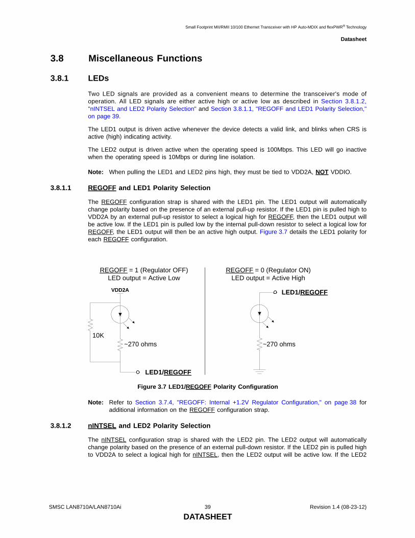
Small Footprint MII/RMII 10/100 Ethernet Transceiver with HP Auto-MDIX and flexPWR® Technology
Datasheet
3.8 Miscellaneous Functions
3.8.1 LEDs
Two LED signals are provided as a convenient means to determine the transceiver's mode ofoperation. All LED signals are either active high or active low as described in Section 3.8.1.2,"nINTSEL and LED2 Polarity Selection" and Section 3.8.1.1, "REGOFF and LED1 Polarity Selection,"on page 39.
The LED1 output is driven active whenever the device detects a valid link, and blinks when CRS isactive (high) indicating activity.
The LED2 output is driven active when the operating speed is 100Mbps. This LED will go inactivewhen the operating speed is 10Mbps or during line isolation.
Note: When pulling the LED1 and LED2 pins high, they must be tied to VDD2A, NOT VDDIO.
3.8.1.1 REGOFF and LED1 Polarity Selection
The REGOFF configuration strap is shared with the LED1 pin. The LED1 output will automaticallychange polarity based on the presence of an external pull-up resistor. If the LED1 pin is pulled high toVDD2A by an external pull-up resistor to select a logical high for REGOFF, then the LED1 output willbe active low. If the LED1 pin is pulled low by the internal pull-down resistor to select a logical low forREGOFF, the LED1 output will then be an active high output. Figure 3.7 details the LED1 polarity foreach REGOFF configuration.
Note: Refer to Section 3.7.4, "REGOFF: Internal +1.2V Regulator Configuration," on page 38 foradditional information on the REGOFF configuration strap.
3.8.1.2 nINTSEL and LED2 Polarity Selection
The nINTSEL configuration strap is shared with the LED2 pin. The LED2 output will automaticallychange polarity based on the presence of an external pull-down resistor. If the LED2 pin is pulled highto VDD2A to select a logical high for nINTSEL, then the LED2 output will be active low. If the LED2
Figure 3.7 LED1/REGOFF Polarity Configuration
LED1/REGOFF
~270 ohms
REGOFF = 0 (Regulator ON)LED output = Active High
~270 ohms
VDD2A
REGOFF = 1 (Regulator OFF)LED output = Active Low
LED1/REGOFF
10K
SMSC LAN8710A/LAN8710Ai 39 Revision 1.4 (08-23-12)
DATASHEET

Small Footprint MII/RMII 10/100 Ethernet Transceiver with HP Auto-MDIX and flexPWR® Technology
Datasheet
pin is pulled low by an external pull-down resistor to select a logical low for nINTSEL, the LED2 outputwill then be an active high output. Figure 3.8 details the LED2 polarity for each nINTSEL configuration.
Note: Refer to Section 3.7.5, "nINTSEL: nINT/TXER/TXD4 Configuration," on page 38 for additionalinformation on the nINTSEL configuration strap.
3.8.2 Variable Voltage I/O
The device’s digital I/O pins are variable voltage, allowing them to take advantage of low power savingsfrom shrinking technologies. These pins can operate from a low I/O voltage of +1.62V up to +3.6V.The applied I/O voltage must maintain its value with a tolerance of ± 10%. Varying the voltage up ordown after the transceiver has completed power-on reset can cause errors in the transceiver operation.Refer to Chapter 5, "Operational Characteristics," on page 66 for additional information.
Note: Input signals must not be driven high before power is applied to the device.
3.8.3 Power-Down Modes
There are two device power-down modes: General Power-Down Mode and Energy Detect Power-Down Mode. These modes are described in the following subsections.
3.8.3.1 General Power-Down
This power-down mode is controlled via the Power Down bit of the Basic Control Register. In thismode, the entire transceiver (except the management interface) is powered-down and remains in thismode as long as the Power Down bit is “1”. When the Power Down bit is cleared, the transceiverpowers up and is automatically reset.
3.8.3.2 Energy Detect Power-Down
This power-down mode is activated by setting the EDPWRDOWN bit of the Mode Control/StatusRegister. In this mode, when no energy is present on the line the transceiver is powered down (exceptfor the management interface, the SQUELCH circuit, and the ENERGYON logic). The ENERGYONlogic is used to detect the presence of valid energy from 100BASE-TX, 10BASE-T, or Auto-negotiationsignals.
In this mode, when the ENERGYON bit of the Mode Control/Status Register is low, the transceiver ispowered-down and nothing is transmitted. When energy is received via link pulses or packets, theENERGYON bit goes high and the transceiver powers-up. The device automatically resets into the
Figure 3.8 LED2/nINTSEL Polarity Configuration
~270 ohms
nINTSEL = 0LED output = Active High
10K
~270 ohms
VDD2A
nINTSEL = 1LED output = Active Low
LED2/nINTSEL
LED2/nINTSEL
Revision 1.4 (08-23-12) 40 SMSC LAN8710A/LAN8710Ai
DATASHEET

Small Footprint MII/RMII 10/100 Ethernet Transceiver with HP Auto-MDIX and flexPWR® Technology
Datasheet
state prior to power-down and asserts the nINT interrupt if the ENERGYON interrupt is enabled in theInterrupt Mask Register. The first and possibly the second packet to activate ENERGYON may be lost.
When the EDPWRDOWN bit of the Mode Control/Status Register is low, energy detect power-down isdisabled.
3.8.4 Isolate Mode
The device data paths may be electrically isolated from the MII/RMII interface by setting the Isolate bitof the Basic Control Register to “1”. In isolation mode, the transceiver does not respond to the TXD,TXEN and TXER inputs, but does respond to management transactions.
Isolation provides a means for multiple transceivers to be connected to the same MII/RMII interfacewithout contention. By default, the transceiver is not isolated (on power-up (Isolate=0).
3.8.5 Resets
The device provides two forms of reset: Hardware and Software. The device registers are reset byboth Hardware and Software resets. Select register bits, indicated as “NASR” in the register definitions,are not cleared by a Software reset. The registers are not reset by the power-down modes describedin Section 3.8.3.
Note: For the first 16us after coming out of reset, the MII/RMII interface will run at 2.5 MHz. After thistime, it will switch to 25 MHz if auto-negotiation is enabled.
3.8.5.1 Hardware Reset
A Hardware reset is asserted by driving the nRST input pin low. When driven, nRST should be heldlow for the minimum time detailed in Section 5.5.3, "Power-On nRST & Configuration Strap Timing,"on page 72 to ensure a proper transceiver reset. During a Hardware reset, an external clock must besupplied to the XTAL1/CLKIN signal.
Note: A hardware reset (nRST assertion) is required following power-up. Refer to Section 5.5.3,"Power-On nRST & Configuration Strap Timing," on page 72 for additional information.
3.8.5.2 Software Reset
A Software reset is activated by setting the Soft Reset bit of the Basic Control Register to “1”. Allregisters bits, except those indicated as “NASR” in the register definitions, are cleared by a Softwarereset. The Soft Reset bit is self-clearing. Per the IEEE 802.3u standard, clause 22 (22.2.4.1.1) the resetprocess will be completed within 0.5s from the setting of this bit.
3.8.6 Carrier Sense
The carrier sense (CRS) is output on the CRS pin in MII mode, and the CRS_DV pin in RMII mode.CRS is a signal defined by the MII specification in the IEEE 802.3u standard. The device asserts CRSbased only on receive activity whenever the transceiver is either in repeater mode or full-duplex mode.Otherwise the transceiver asserts CRS based on either transmit or receive activity.
The carrier sense logic uses the encoded, unscrambled data to determine carrier activity status. Itactivates carrier sense with the detection of 2 non-contiguous zeros within any 10 bit span. Carriersense terminates if a span of 10 consecutive ones is detected before a /J/K/ Start-of Stream Delimiterpair. If an SSD pair is detected, carrier sense is asserted until either /T/R/ End–of-Stream Delimiterpair or a pair of IDLE symbols is detected. Carrier is negated after the /T/ symbol or the first IDLE. If/T/ is not followed by /R/, then carrier is maintained. Carrier is treated similarly for IDLE followed bysome non-IDLE symbol.
SMSC LAN8710A/LAN8710Ai 41 Revision 1.4 (08-23-12)
DATASHEET
Small Footprint MII/RMII 10/100 Ethernet Transceiver with HP Auto-MDIX and flexPWR® Technology
Datasheet
3.8.7 Collision Detect
A collision is the occurrence of simultaneous transmit and receive operations. The COL output isasserted to indicate that a collision has been detected. COL remains active for the duration of thecollision. COL is changed asynchronously to both RXCLK and TXCLK. The COL output becomesinactive during full duplex mode.
The COL may be tested by setting the Collision Test bit of the Basic Control Register to “1”. Thisenables the collision test. COL will be asserted within 512 bit times of TXEN rising and will be de-asserted within 4 bit times of TXEN falling.
3.8.8 Link Integrity Test
The device performs the link integrity test as outlined in the IEEE 802.3u (Clause 24-15) Link Monitorstate diagram. The link status is multiplexed with the 10Mbps link status to form the Link Status bit inthe Basic Status Register and to drive the LINK LED (LED1).
The DSP indicates a valid MLT-3 waveform present on the RXP and RXN signals as defined by theANSI X3.263 TP-PMD standard, to the Link Monitor state-machine, using the internal DATA_VALIDsignal. When DATA_VALID is asserted, the control logic moves into a Link-Ready state and waits foran enable from the auto-negotiation block. When received, the Link-Up state is entered, and theTransmit and Receive logic blocks become active. Should auto-negotiation be disabled, the linkintegrity logic moves immediately to the Link-Up state when the DATA_VALID is asserted.
To allow the line to stabilize, the link integrity logic will wait a minimum of 330 μsec from the timeDATA_VALID is asserted until the Link-Ready state is entered. Should the DATA_VALID input benegated at any time, this logic will immediately negate the Link signal and enter the Link-Down state.
When the 10/100 digital block is in 10BASE-T mode, the link status is derived from the 10BASE-Treceiver logic.
3.8.9 Loopback Operation
The device may be configured for near-end loopback and far loopback. These loopback modes aredetailed in the following subsections.
3.8.9.1 Near-end Loopback
Near-end loopback mode sends the digital transmit data back out the receive data signals for testingpurposes, as indicated by the blue arrows in Figure 3.9. The near-end loopback mode is enabled bysetting the Loopback bit of the Basic Control Register to “1”. A large percentage of the digital circuitryis operational in near-end loopback mode because data is routed through the PCS and PMA layersinto the PMD sublayer before it is looped back. The COL signal will be inactive in this mode, unless
Revision 1.4 (08-23-12) 42 SMSC LAN8710A/LAN8710Ai
DATASHEET

Small Footprint MII/RMII 10/100 Ethernet Transceiver with HP Auto-MDIX and flexPWR® Technology
Datasheet
Collision Test is enabled in the Basic Control Register. The transmitters are powered down regardlessof the state of TXEN.
3.8.9.2 Far Loopback
Far loopback is a special test mode for MDI (analog) loopback as indicated by the blue arrows inFigure 3.11. The far loopback mode is enabled by setting the FARLOOPBACK bit of the ModeControl/Status Register to “1”. In this mode, data that is received from the link partner on the MDI islooped back out to the link partner. The digital interface signals on the local MAC interface are isolated.
Note: This special test mode is only available when operating in RMII mode.
3.8.9.3 Connector Loopback
The device maintains reliable transmission over very short cables, and can be tested in a connectorloopback as shown in Figure 3.11. An RJ45 loopback cable can be used to route the transmit signals
Figure 3.9 Near-end Loopback Block Diagram
Figure 3.10 Far Loopback Block Diagram
SMSCEthernet Transceiver
10/100Ethernet
MAC
CAT-5XFMR
DigitalRXD
TXD
AnalogRX
TXX
X
Far-end system
SMSCEthernet Transceiver
10/100Ethernet
MAC
CAT-5XFMR
DigitalRXD
TXD
AnalogRX
TXLink
PartnerX
X
SMSC LAN8710A/LAN8710Ai 43 Revision 1.4 (08-23-12)
DATASHEET
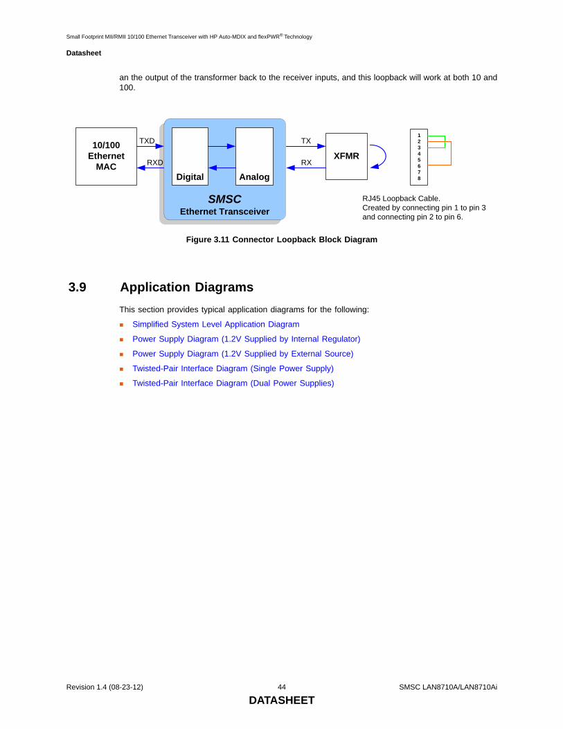
Small Footprint MII/RMII 10/100 Ethernet Transceiver with HP Auto-MDIX and flexPWR® Technology
Datasheet
an the output of the transformer back to the receiver inputs, and this loopback will work at both 10 and100.
3.9 Application DiagramsThis section provides typical application diagrams for the following:
Simplified System Level Application Diagram
Power Supply Diagram (1.2V Supplied by Internal Regulator)
Power Supply Diagram (1.2V Supplied by External Source)
Twisted-Pair Interface Diagram (Single Power Supply)
Twisted-Pair Interface Diagram (Dual Power Supplies)
Figure 3.11 Connector Loopback Block Diagram
SMSCEthernet Transceiver
10/100Ethernet
MACXFMR
DigitalRXD
TXD
AnalogRX
TX12345678
RJ45 Loopback Cable.Created by connecting pin 1 to pin 3 and connecting pin 2 to pin 6.
Revision 1.4 (08-23-12) 44 SMSC LAN8710A/LAN8710Ai
DATASHEET

Small Footprint MII/RMII 10/100 Ethernet Transceiver with HP Auto-MDIX and flexPWR® Technology
Datasheet
3.9.1 Simplified System Level Application Diagram
Figure 3.12 Simplified System Level Application Diagram
LAN8710A/LAN8710Ai10/100 PHY
32-QFNMII
TXP
TXN
Mag RJ45
RXP
RXN
25MHz
XTAL1/CLKIN
XTAL2
TXD[3:0]
4
RXD[3:0]
RXCLKRXDV
4
MII
LED[2:1]
2
Interface
MDIOMDCnINT
nRST
TXCLKTXERTXEN
SMSC LAN8710A/LAN8710Ai 45 Revision 1.4 (08-23-12)
DATASHEET
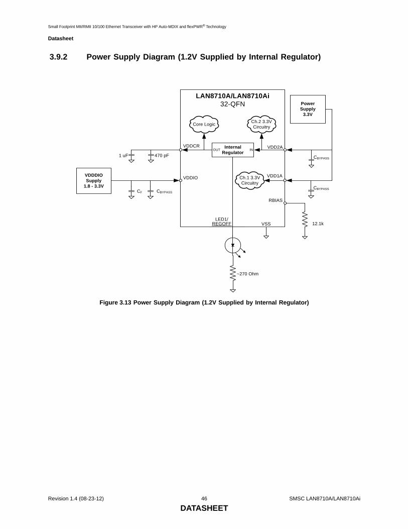
Small Footprint MII/RMII 10/100 Ethernet Transceiver with HP Auto-MDIX and flexPWR® Technology
Datasheet
3.9.2 Power Supply Diagram (1.2V Supplied by Internal Regulator)
Figure 3.13 Power Supply Diagram (1.2V Supplied by Internal Regulator)
LAN8710A/LAN8710Ai32-QFN
RBIAS
VSS 12.1k
VDD2A
CBYPASS
CBYPASS
VDD1AVDDIO
CBYPASSCF
VDDDIOSupply
1.8 - 3.3V
PowerSupply
3.3V
VDDCR
LED1/REGOFF
~270 Ohm
Core Logic
Internal Regulator
Ch.2 3.3V Circuitry
INOUT
Ch.1 3.3V Circuitry
470 pF1 uF
Revision 1.4 (08-23-12) 46 SMSC LAN8710A/LAN8710Ai
DATASHEET

Small Footprint MII/RMII 10/100 Ethernet Transceiver with HP Auto-MDIX and flexPWR® Technology
Datasheet
3.9.3 Power Supply Diagram (1.2V Supplied by External Source)
Figure 3.14 Power Supply Diagram (1.2V Supplied by External Source)
LAN8710A/LAN8710Ai32-QFN
RBIAS
VSS 12.1k
VDD2A
CBYPASS
CBYPASS
VDD1AVDDIO
CBYPASSCF
VDDDIOSupply
1.8 - 3.3V
PowerSupply
3.3V
VDDCR
LED1/REGOFF
Core Logic
Internal Regulator
(Disabled)
Ch.2 3.3V Circuitry
INOUT
Ch.1 3.3V Circuitry
VDDCRSupply
1.2V
~270 Ohm
10k
470 pF1 uF
SMSC LAN8710A/LAN8710Ai 47 Revision 1.4 (08-23-12)
DATASHEET
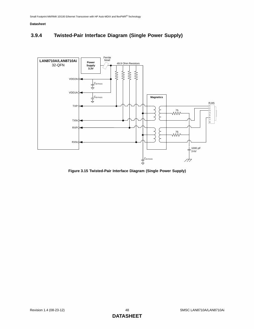
Small Footprint MII/RMII 10/100 Ethernet Transceiver with HP Auto-MDIX and flexPWR® Technology
Datasheet
3.9.4 Twisted-Pair Interface Diagram (Single Power Supply)
Figure 3.15 Twisted-Pair Interface Diagram (Single Power Supply)
Magnetics
LAN8710A/LAN8710Ai32-QFN
VDD2ACBYPASS
TXP
TXN
PowerSupply
3.3V
12345678
1000 pF3 kV
RJ45
75
75RXP
RXN
CBYPASS
VDD1ACBYPASS
49.9 Ohm Resistors
Ferrite bead
Revision 1.4 (08-23-12) 48 SMSC LAN8710A/LAN8710Ai
DATASHEET
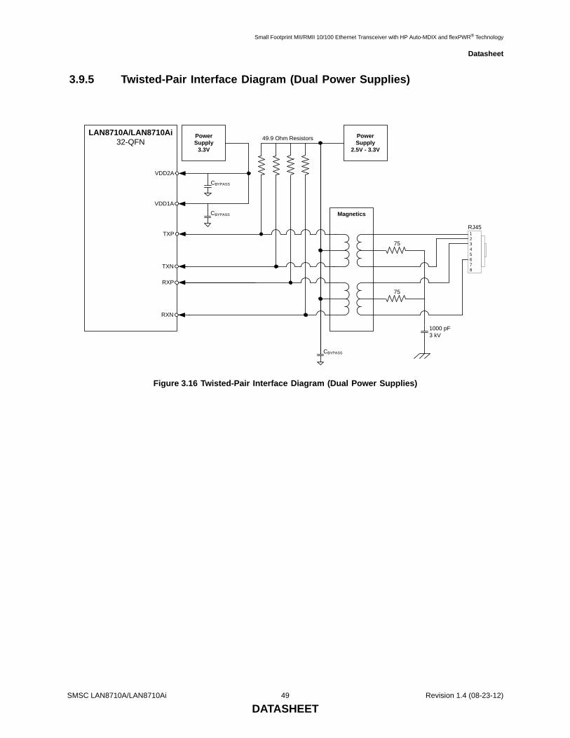
Small Footprint MII/RMII 10/100 Ethernet Transceiver with HP Auto-MDIX and flexPWR® Technology
Datasheet
3.9.5 Twisted-Pair Interface Diagram (Dual Power Supplies)
Figure 3.16 Twisted-Pair Interface Diagram (Dual Power Supplies)
Magnetics
LAN8710A/LAN8710Ai32-QFN
VDD2ACBYPASS
TXP
TXN
PowerSupply
3.3V
12345678
1000 pF3 kV
RJ45
75
75RXP
RXN
CBYPASS
VDD1ACBYPASS
49.9 Ohm Resistors PowerSupply
2.5V - 3.3V
SMSC LAN8710A/LAN8710Ai 49 Revision 1.4 (08-23-12)
DATASHEET

Small Footprint MII/RMII 10/100 Ethernet Transceiver with HP Auto-MDIX and flexPWR® Technology
Datasheet
Chapter 4 Register Descriptions
This chapter describes the various control and status registers (CSR’s). All registers follow the IEEE802.3 (clause 22.2.4) management register set. All functionality and bit definitions comply with thesestandards. The IEEE 802.3 specified register index (in decimal) is included with each register definition,allowing for addressing of these registers via the Serial Management Interface (SMI) protocol.
4.1 Register NomenclatureTable 4.1 describes the register bit attribute notation used throughout this document.
Many of these register bit notations can be combined. Some examples of this are shown below:
R/W: Can be written. Will return current setting on a read.
R/WAC: Will return current setting on a read. Writing anything clears the bit.
Table 4.1 Register Bit Types
REGISTER BIT TYPE NOTATION REGISTER BIT DESCRIPTION
R Read: A register or bit with this attribute can be read.
W Read: A register or bit with this attribute can be written.
RO Read only: Read only. Writes have no effect.
WO Write only: If a register or bit is write-only, reads will return unspecified data.
WC Write One to Clear: writing a one clears the value. Writing a zero has no effect
WAC Write Anything to Clear: writing anything clears the value.
RC Read to Clear: Contents is cleared after the read. Writes have no effect.
LL Latch Low: Clear on read of register.
LH Latch High: Clear on read of register.
SC Self-Clearing: Contents are self-cleared after the being set. Writes of zero have no effect. Contents can be read.
SS Self-Setting: Contents are self-setting after being cleared. Writes of one have no effect. Contents can be read.
RO/LH Read Only, Latch High: Bits with this attribute will stay high until the bit is read. After it is read, the bit will either remain high if the high condition remains, or will go low if the high condition has been removed. If the bit has not been read, the bit will remain high regardless of a change to the high condition. This mode is used in some Ethernet PHY registers.
NASR Not Affected by Software Reset. The state of NASR bits do not change on assertion of a software reset.
RESERVED Reserved Field: Reserved fields must be written with zeros to ensure future compatibility. The value of reserved bits is not guaranteed on a read.
Revision 1.4 (08-23-12) 50 SMSC LAN8710A/LAN8710Ai
DATASHEET

Small Footprint MII/RMII 10/100 Ethernet Transceiver with HP Auto-MDIX and flexPWR® Technology
Datasheet
4.2 Control and Status RegistersTable 4.2 provides a list of supported registers. Register details, including bit definitions, are providedin the proceeding subsections.
Table 4.2 SMI Register Map
REGISTER INDEX(DECIMAL) REGISTER NAME GROUP
0 Basic Control Register Basic
1 Basic Status Register Basic
2 PHY Identifier 1 Extended
3 PHY Identifier 2 Extended
4 Auto-Negotiation Advertisement Register Extended
5 Auto-Negotiation Link Partner Ability Register Extended
6 Auto-Negotiation Expansion Register Extended
17 Mode Control/Status Register Vendor-specific
18 Special Modes Vendor-specific
26 Symbol Error Counter Register Vendor-specific
27 Control / Status Indication Register Vendor-specific
29 Interrupt Source Register Vendor-specific
30 Interrupt Mask Register Vendor-specific
31 PHY Special Control/Status Register Vendor-specific
SMSC LAN8710A/LAN8710Ai 51 Revision 1.4 (08-23-12)
DATASHEET
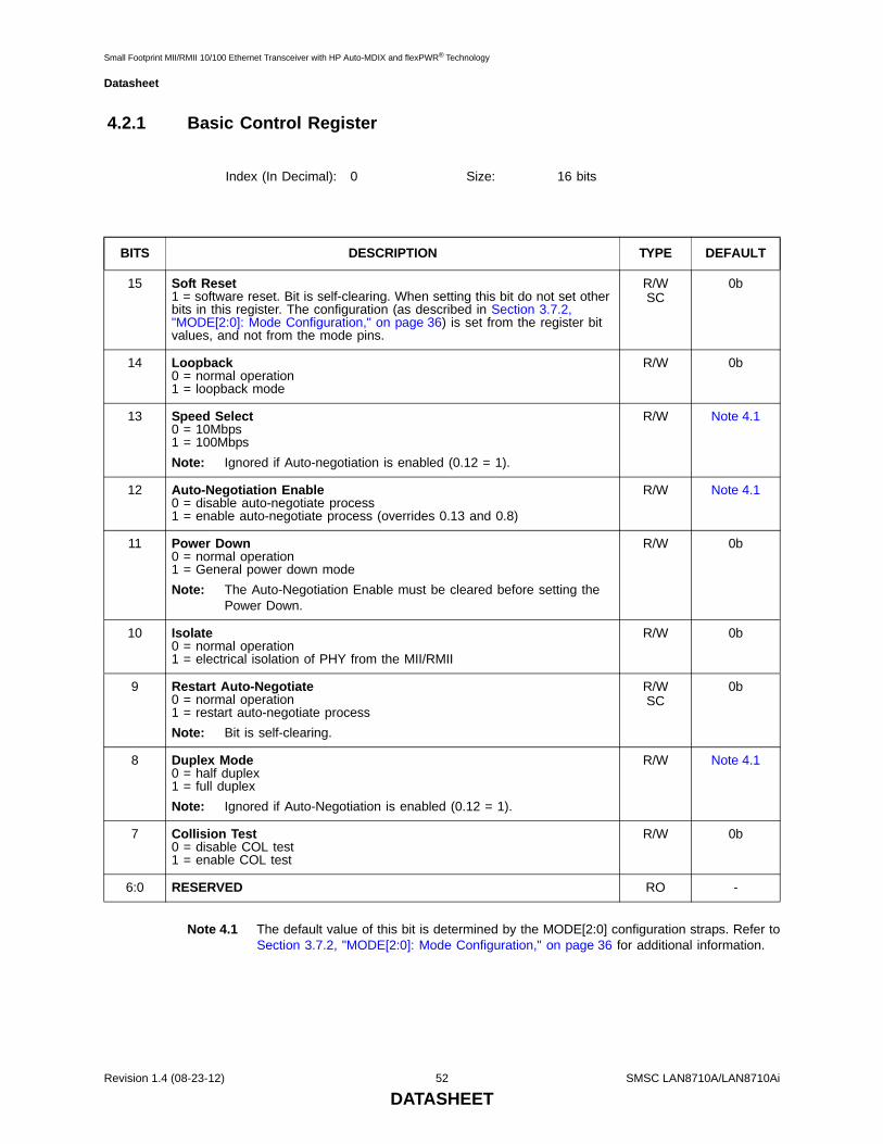
Small Footprint MII/RMII 10/100 Ethernet Transceiver with HP Auto-MDIX and flexPWR® Technology
Datasheet
4.2.1 Basic Control Register
Note 4.1 The default value of this bit is determined by the MODE[2:0] configuration straps. Refer toSection 3.7.2, "MODE[2:0]: Mode Configuration," on page 36 for additional information.
Index (In Decimal): 0 Size: 16 bits
BITS DESCRIPTION TYPE DEFAULT
15 Soft Reset1 = software reset. Bit is self-clearing. When setting this bit do not set other bits in this register. The configuration (as described in Section 3.7.2, "MODE[2:0]: Mode Configuration," on page 36) is set from the register bit values, and not from the mode pins.
R/WSC
0b
14 Loopback0 = normal operation1 = loopback mode
R/W 0b
13 Speed Select0 = 10Mbps1 = 100MbpsNote: Ignored if Auto-negotiation is enabled (0.12 = 1).
R/W Note 4.1
12 Auto-Negotiation Enable0 = disable auto-negotiate process1 = enable auto-negotiate process (overrides 0.13 and 0.8)
R/W Note 4.1
11 Power Down0 = normal operation 1 = General power down modeNote: The Auto-Negotiation Enable must be cleared before setting the
Power Down.
R/W 0b
10 Isolate0 = normal operation1 = electrical isolation of PHY from the MII/RMII
R/W 0b
9 Restart Auto-Negotiate0 = normal operation1 = restart auto-negotiate processNote: Bit is self-clearing.
R/WSC
0b
8 Duplex Mode0 = half duplex1 = full duplexNote: Ignored if Auto-Negotiation is enabled (0.12 = 1).
R/W Note 4.1
7 Collision Test0 = disable COL test1 = enable COL test
R/W 0b
6:0 RESERVED RO -
Revision 1.4 (08-23-12) 52 SMSC LAN8710A/LAN8710Ai
DATASHEET
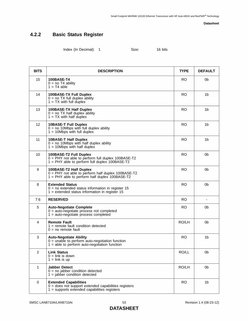
Small Footprint MII/RMII 10/100 Ethernet Transceiver with HP Auto-MDIX and flexPWR® Technology
Datasheet
4.2.2 Basic Status Register
Index (In Decimal): 1 Size: 16 bits
BITS DESCRIPTION TYPE DEFAULT
15 100BASE-T40 = no T4 ability1 = T4 able
RO 0b
14 100BASE-TX Full Duplex0 = no TX full duplex ability1 = TX with full duplex
RO 1b
13 100BASE-TX Half Duplex0 = no TX half duplex ability1 = TX with half duplex
RO 1b
12 10BASE-T Full Duplex0 = no 10Mbps with full duplex ability1 = 10Mbps with full duplex
RO 1b
11 10BASE-T Half Duplex0 = no 10Mbps with half duplex ability1 = 10Mbps with half duplex
RO 1b
10 100BASE-T2 Full Duplex0 = PHY not able to perform full duplex 100BASE-T21 = PHY able to perform full duplex 100BASE-T2
RO 0b
9 100BASE-T2 Half Duplex0 = PHY not able to perform half duplex 100BASE-T21 = PHY able to perform half duplex 100BASE-T2
RO 0b
8 Extended Status0 = no extended status information in register 151 = extended status information in register 15
RO 0b
7:6 RESERVED RO -
5 Auto-Negotiate Complete0 = auto-negotiate process not completed1 = auto-negotiate process completed
RO 0b
4 Remote Fault1 = remote fault condition detected0 = no remote fault
RO/LH 0b
3 Auto-Negotiate Ability0 = unable to perform auto-negotiation function1 = able to perform auto-negotiation function
RO 1b
2 Link Status0 = link is down1 = link is up
RO/LL 0b
1 Jabber Detect0 = no jabber condition detected1 = jabber condition detected
RO/LH 0b
0 Extended Capabilities0 = does not support extended capabilities registers1 = supports extended capabilities registers
RO 1b
SMSC LAN8710A/LAN8710Ai 53 Revision 1.4 (08-23-12)
DATASHEET
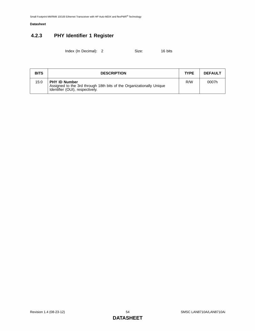
Small Footprint MII/RMII 10/100 Ethernet Transceiver with HP Auto-MDIX and flexPWR® Technology
Datasheet
4.2.3 PHY Identifier 1 Register
Index (In Decimal): 2 Size: 16 bits
BITS DESCRIPTION TYPE DEFAULT
15:0 PHY ID NumberAssigned to the 3rd through 18th bits of the Organizationally Unique Identifier (OUI), respectively.
R/W 0007h
Revision 1.4 (08-23-12) 54 SMSC LAN8710A/LAN8710Ai
DATASHEET
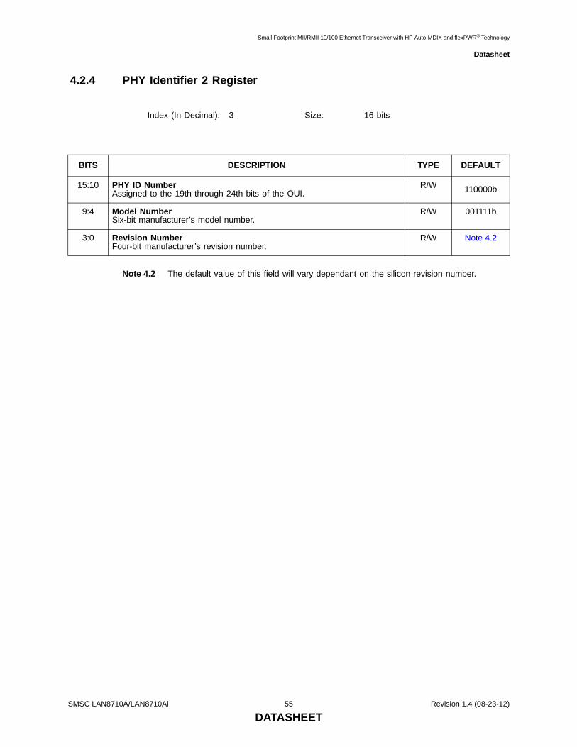
Small Footprint MII/RMII 10/100 Ethernet Transceiver with HP Auto-MDIX and flexPWR® Technology
Datasheet
4.2.4 PHY Identifier 2 Register
Note 4.2 The default value of this field will vary dependant on the silicon revision number.
Index (In Decimal): 3 Size: 16 bits
BITS DESCRIPTION TYPE DEFAULT
15:10 PHY ID NumberAssigned to the 19th through 24th bits of the OUI.
R/W 110000b
9:4 Model NumberSix-bit manufacturer’s model number.
R/W 001111b
3:0 Revision NumberFour-bit manufacturer’s revision number.
R/W Note 4.2
SMSC LAN8710A/LAN8710Ai 55 Revision 1.4 (08-23-12)
DATASHEET
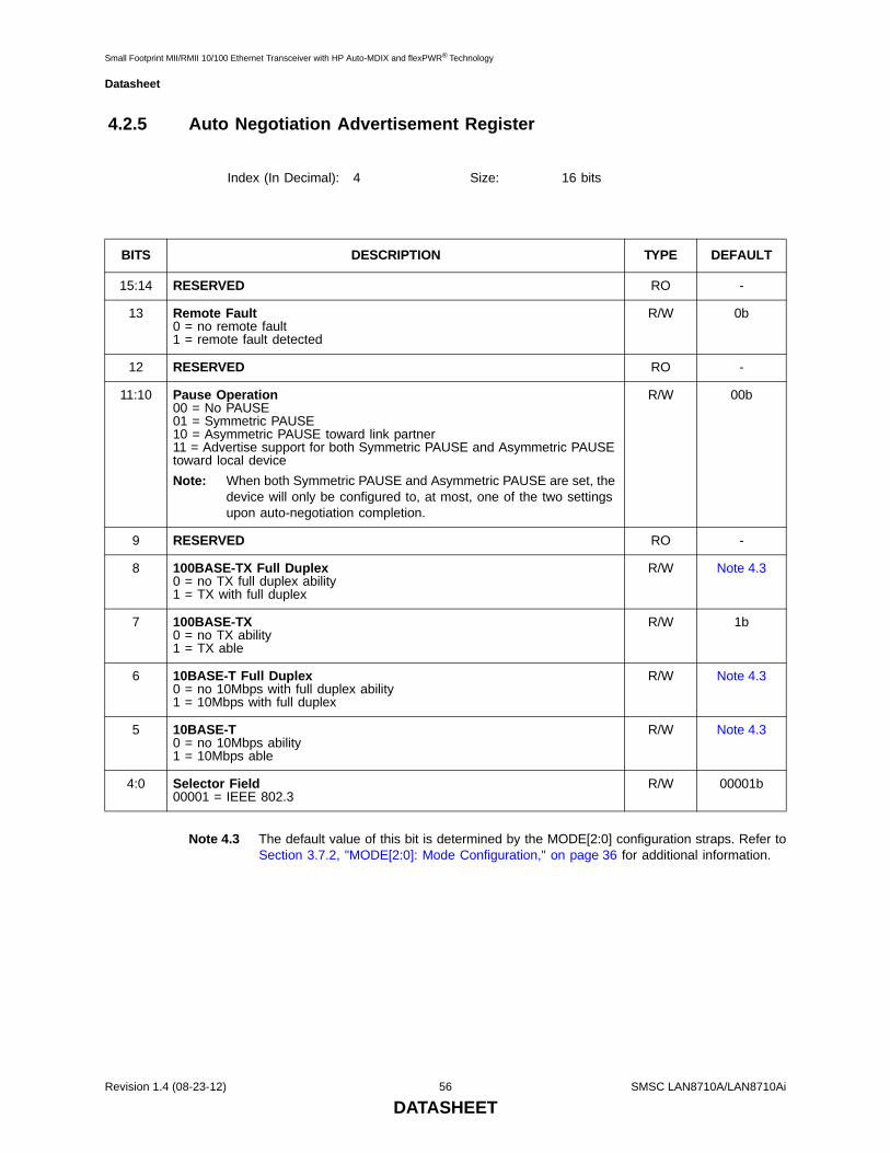
Small Footprint MII/RMII 10/100 Ethernet Transceiver with HP Auto-MDIX and flexPWR® Technology
Datasheet
4.2.5 Auto Negotiation Advertisement Register
Note 4.3 The default value of this bit is determined by the MODE[2:0] configuration straps. Refer toSection 3.7.2, "MODE[2:0]: Mode Configuration," on page 36 for additional information.
Index (In Decimal): 4 Size: 16 bits
BITS DESCRIPTION TYPE DEFAULT
15:14 RESERVED RO -
13 Remote Fault0 = no remote fault1 = remote fault detected
R/W 0b
12 RESERVED RO -
11:10 Pause Operation00 = No PAUSE 01 = Symmetric PAUSE10 = Asymmetric PAUSE toward link partner11 = Advertise support for both Symmetric PAUSE and Asymmetric PAUSE toward local deviceNote: When both Symmetric PAUSE and Asymmetric PAUSE are set, the
device will only be configured to, at most, one of the two settings upon auto-negotiation completion.
R/W 00b
9 RESERVED RO -
8 100BASE-TX Full Duplex0 = no TX full duplex ability1 = TX with full duplex
R/W Note 4.3
7 100BASE-TX0 = no TX ability1 = TX able
R/W 1b
6 10BASE-T Full Duplex0 = no 10Mbps with full duplex ability1 = 10Mbps with full duplex
R/W Note 4.3
5 10BASE-T0 = no 10Mbps ability1 = 10Mbps able
R/W Note 4.3
4:0 Selector Field00001 = IEEE 802.3
R/W 00001b
Revision 1.4 (08-23-12) 56 SMSC LAN8710A/LAN8710Ai
DATASHEET
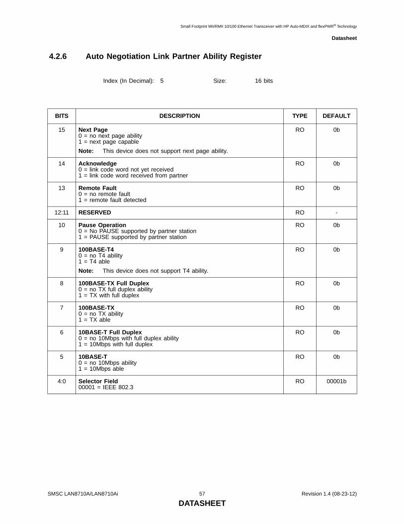
Small Footprint MII/RMII 10/100 Ethernet Transceiver with HP Auto-MDIX and flexPWR® Technology
Datasheet
4.2.6 Auto Negotiation Link Partner Ability Register
Index (In Decimal): 5 Size: 16 bits
BITS DESCRIPTION TYPE DEFAULT
15 Next Page0 = no next page ability1 = next page capableNote: This device does not support next page ability.
RO 0b
14 Acknowledge0 = link code word not yet received1 = link code word received from partner
RO 0b
13 Remote Fault0 = no remote fault1 = remote fault detected
RO 0b
12:11 RESERVED RO -
10 Pause Operation0 = No PAUSE supported by partner station1 = PAUSE supported by partner station
RO 0b
9 100BASE-T40 = no T4 ability1 = T4 ableNote: This device does not support T4 ability.
RO 0b
8 100BASE-TX Full Duplex0 = no TX full duplex ability1 = TX with full duplex
RO 0b
7 100BASE-TX0 = no TX ability1 = TX able
RO 0b
6 10BASE-T Full Duplex0 = no 10Mbps with full duplex ability1 = 10Mbps with full duplex
RO 0b
5 10BASE-T0 = no 10Mbps ability1 = 10Mbps able
RO 0b
4:0 Selector Field00001 = IEEE 802.3
RO 00001b
SMSC LAN8710A/LAN8710Ai 57 Revision 1.4 (08-23-12)
DATASHEET

Small Footprint MII/RMII 10/100 Ethernet Transceiver with HP Auto-MDIX and flexPWR® Technology
Datasheet
4.2.7 Auto Negotiation Expansion Register
Index (In Decimal): 6 Size: 16 bits
BITS DESCRIPTION TYPE DEFAULT
15:5 RESERVED RO -
4 Parallel Detection Fault0 = no fault detected by parallel detection logic1 = fault detected by parallel detection logic
RO/LH 0b
3 Link Partner Next Page Able0 = link partner does not have next page ability1 = link partner has next page ability
RO 0b
2 Next Page Able0 = local device does not have next page ability1 = local device has next page ability
RO 0b
1 Page Received0 = new page not yet received1 = new page received
RO/LH 0b
0 Link Partner Auto-Negotiation Able0 = link partner does not have auto-negotiation ability1 = link partner has auto-negotiation ability
RO 0b
Revision 1.4 (08-23-12) 58 SMSC LAN8710A/LAN8710Ai
DATASHEET
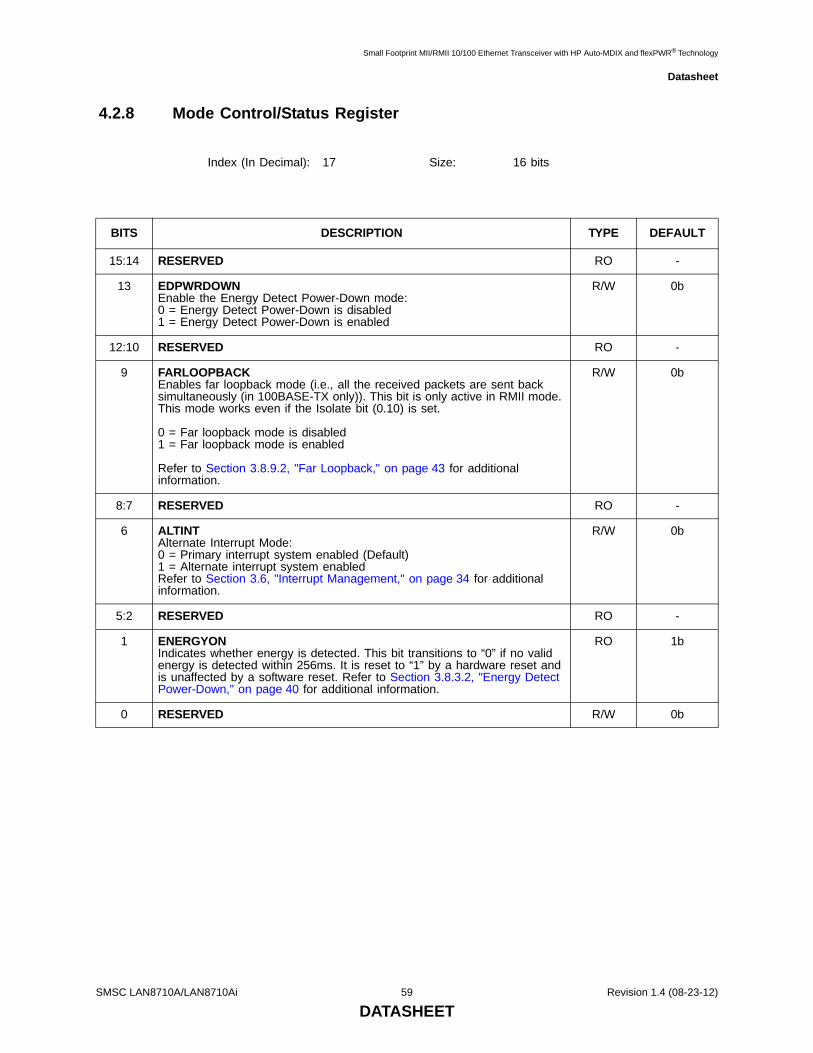
Small Footprint MII/RMII 10/100 Ethernet Transceiver with HP Auto-MDIX and flexPWR® Technology
Datasheet
4.2.8 Mode Control/Status Register
Index (In Decimal): 17 Size: 16 bits
BITS DESCRIPTION TYPE DEFAULT
15:14 RESERVED RO -
13 EDPWRDOWNEnable the Energy Detect Power-Down mode:0 = Energy Detect Power-Down is disabled1 = Energy Detect Power-Down is enabled
R/W 0b
12:10 RESERVED RO -
9 FARLOOPBACKEnables far loopback mode (i.e., all the received packets are sent back simultaneously (in 100BASE-TX only)). This bit is only active in RMII mode. This mode works even if the Isolate bit (0.10) is set.
0 = Far loopback mode is disabled1 = Far loopback mode is enabled
Refer to Section 3.8.9.2, "Far Loopback," on page 43 for additional information.
R/W 0b
8:7 RESERVED RO -
6 ALTINTAlternate Interrupt Mode:0 = Primary interrupt system enabled (Default)1 = Alternate interrupt system enabledRefer to Section 3.6, "Interrupt Management," on page 34 for additional information.
R/W 0b
5:2 RESERVED RO -
1 ENERGYONIndicates whether energy is detected. This bit transitions to “0” if no valid energy is detected within 256ms. It is reset to “1” by a hardware reset and is unaffected by a software reset. Refer to Section 3.8.3.2, "Energy Detect Power-Down," on page 40 for additional information.
RO 1b
0 RESERVED R/W 0b
SMSC LAN8710A/LAN8710Ai 59 Revision 1.4 (08-23-12)
DATASHEET

Small Footprint MII/RMII 10/100 Ethernet Transceiver with HP Auto-MDIX and flexPWR® Technology
Datasheet
4.2.9 Special Modes Register
Note 4.4 The default value of this field is determined by the RMIISEL configuration strap. Refer toSection 3.7.3, "RMIISEL: MII/RMII Mode Configuration," on page 37 for additionalinformation.
Note 4.5 The default value of this field is determined by the MODE[2:0] configuration straps. Referto Section 3.7.2, "MODE[2:0]: Mode Configuration," on page 36 for additional information.
Note 4.6 The default value of this field is determined by the PHYAD[2:0] configuration straps. Referto Section 3.7.1, "PHYAD[2:0]: PHY Address Configuration," on page 36 for additionalinformation.
Index (In Decimal): 18 Size: 16 bits
BITS DESCRIPTION TYPE DEFAULT
15 RESERVED RO -
14 MIIMODEReflects the mode of the digital interface:0 = MII Mode1 = RMII ModeNote: When writing to this register, the default value of this bit must
always be written back.
R/WNASR
Note 4.4
13:8 RESERVED RO -
7:5 MODETransceiver mode of operation. Refer to Section 3.7.2, "MODE[2:0]: Mode Configuration," on page 36 for additional details.
R/WNASR
Note 4.5
4:0 PHYADPHY Address. The PHY Address is used for the SMI address and for initialization of the Cipher (Scrambler) key. Refer to Section 3.7.1, "PHYAD[2:0]: PHY Address Configuration," on page 36 for additional details.
R/WNASR
Note 4.6
Revision 1.4 (08-23-12) 60 SMSC LAN8710A/LAN8710Ai
DATASHEET
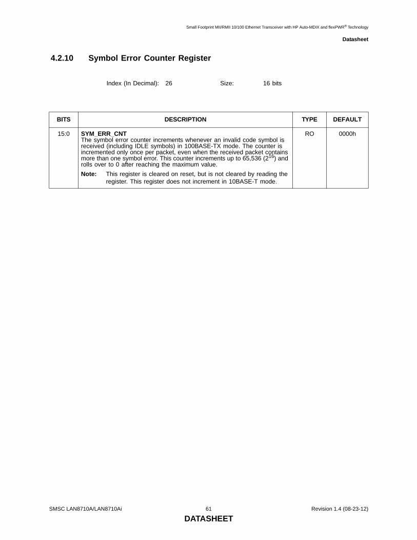
Small Footprint MII/RMII 10/100 Ethernet Transceiver with HP Auto-MDIX and flexPWR® Technology
Datasheet
4.2.10 Symbol Error Counter Register
Index (In Decimal): 26 Size: 16 bits
BITS DESCRIPTION TYPE DEFAULT
15:0 SYM_ERR_CNTThe symbol error counter increments whenever an invalid code symbol is received (including IDLE symbols) in 100BASE-TX mode. The counter is incremented only once per packet, even when the received packet contains more than one symbol error. This counter increments up to 65,536 (216) and rolls over to 0 after reaching the maximum value. Note: This register is cleared on reset, but is not cleared by reading the
register. This register does not increment in 10BASE-T mode.
RO 0000h
SMSC LAN8710A/LAN8710Ai 61 Revision 1.4 (08-23-12)
DATASHEET
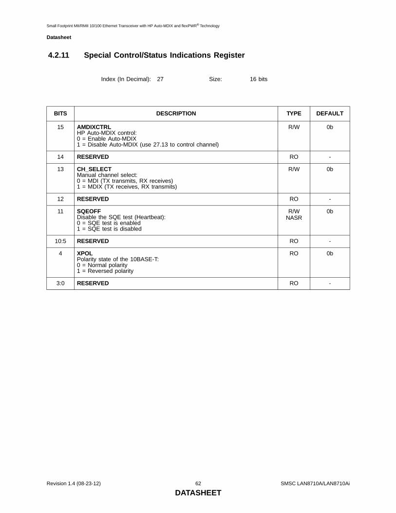
Small Footprint MII/RMII 10/100 Ethernet Transceiver with HP Auto-MDIX and flexPWR® Technology
Datasheet
4.2.11 Special Control/Status Indications Register
Index (In Decimal): 27 Size: 16 bits
BITS DESCRIPTION TYPE DEFAULT
15 AMDIXCTRLHP Auto-MDIX control:0 = Enable Auto-MDIX1 = Disable Auto-MDIX (use 27.13 to control channel)
R/W 0b
14 RESERVED RO -
13 CH_SELECTManual channel select:0 = MDI (TX transmits, RX receives)1 = MDIX (TX receives, RX transmits)
R/W 0b
12 RESERVED RO -
11 SQEOFFDisable the SQE test (Heartbeat):0 = SQE test is enabled1 = SQE test is disabled
R/WNASR
0b
10:5 RESERVED RO -
4 XPOLPolarity state of the 10BASE-T:0 = Normal polarity1 = Reversed polarity
RO 0b
3:0 RESERVED RO -
Revision 1.4 (08-23-12) 62 SMSC LAN8710A/LAN8710Ai
DATASHEET
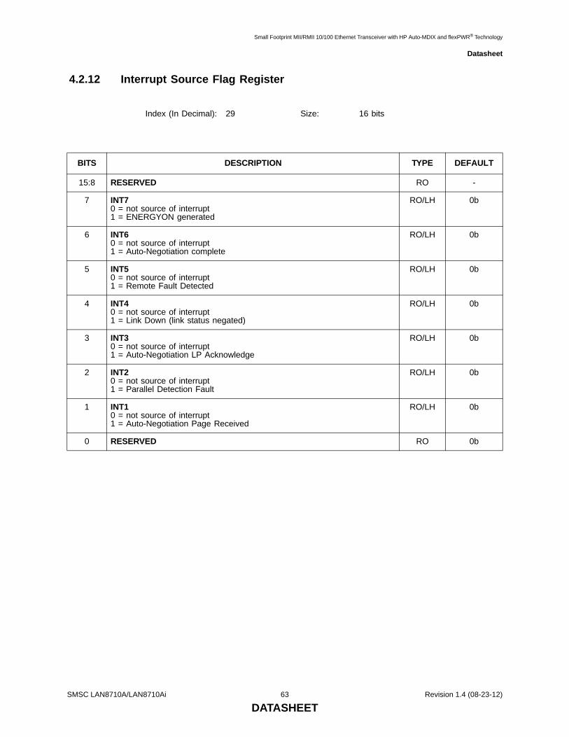
Small Footprint MII/RMII 10/100 Ethernet Transceiver with HP Auto-MDIX and flexPWR® Technology
Datasheet
4.2.12 Interrupt Source Flag Register
Index (In Decimal): 29 Size: 16 bits
BITS DESCRIPTION TYPE DEFAULT
15:8 RESERVED RO -
7 INT70 = not source of interrupt1 = ENERGYON generated
RO/LH 0b
6 INT60 = not source of interrupt1 = Auto-Negotiation complete
RO/LH 0b
5 INT50 = not source of interrupt1 = Remote Fault Detected
RO/LH 0b
4 INT40 = not source of interrupt1 = Link Down (link status negated)
RO/LH 0b
3 INT30 = not source of interrupt1 = Auto-Negotiation LP Acknowledge
RO/LH 0b
2 INT20 = not source of interrupt1 = Parallel Detection Fault
RO/LH 0b
1 INT10 = not source of interrupt1 = Auto-Negotiation Page Received
RO/LH 0b
0 RESERVED RO 0b
SMSC LAN8710A/LAN8710Ai 63 Revision 1.4 (08-23-12)
DATASHEET

Small Footprint MII/RMII 10/100 Ethernet Transceiver with HP Auto-MDIX and flexPWR® Technology
Datasheet
4.2.13 Interrupt Mask Register
Index (In Decimal): 30 Size: 16 bits
BITS DESCRIPTION TYPE DEFAULT
15:8 RESERVED RO -
7:1 Mask Bits0 = interrupt source is masked1 = interrupt source is enabledNote: Refer to Section 4.2.12, "Interrupt Source Flag Register," on
page 63 for details on the corresponding interrupt definitions.
R/W 0000000b
0 RESERVED RO -
Revision 1.4 (08-23-12) 64 SMSC LAN8710A/LAN8710Ai
DATASHEET

Small Footprint MII/RMII 10/100 Ethernet Transceiver with HP Auto-MDIX and flexPWR® Technology
Datasheet
4.2.14 PHY Special Control/Status Register
Index (In Decimal): 31 Size: 16 bits
BITS DESCRIPTION TYPE DEFAULT
15:13 RESERVED RO -
12 AutodoneAuto-negotiation done indication:0 = Auto-negotiation is not done or disabled (or not active)1 = Auto-negotiation is done
RO 0b
11:7 RESERVED R/W -
6 Enable 4B5B0 = bypass encoder/decoder1 = enable 4B5B encoding/decoding. MAC Interface must be configured in MII mode.
R/W 1b
5 RESERVED RO -
4:2 Speed IndicationHCDSPEED value:001 = 10BASE-T half-duplex101 = 10BASE-T full-duplex010 = 100BASE-TX half-duplex110 = 100BASE-TX full-duplex
RO XXX
1:0 RESERVED RO -
SMSC LAN8710A/LAN8710Ai 65 Revision 1.4 (08-23-12)
DATASHEET
Small Footprint MII/RMII 10/100 Ethernet Transceiver with HP Auto-MDIX and flexPWR® Technology
Datasheet
Chapter 5 Operational Characteristics
5.1 Absolute Maximum Ratings*Supply Voltage (VDDIO, VDD1A, VDD2A) (Note 5.1) . . . . . . . . . . . . . . . . . . . . . . . . . . . -0.5V to +3.6V
Digital Core Supply Voltage (VDDCR) (Note 5.1) . . . . . . . . . . . . . . . . . . . . . . . . . . . . . . -0.5V to +1.5V
Ethernet Magnetics Supply Voltage . . . . . . . . . . . . . . . . . . . . . . . . . . . . . . . . . . . . . . . . . -0.5V to +3.6V
Positive voltage on signal pins, with respect to ground (Note 5.2) . . . . . . . . . . . . . . . . . . . . . . . . . . +6V
Negative voltage on signal pins, with respect to ground (Note 5.3) . . . . . . . . . . . . . . . . . . . . . . . . -0.5V
Positive voltage on XTAL1/CLKIN, with respect to ground . . . . . . . . . . . . . . . . . . . . . . . . . . . . . . +4.6V
Positive voltage on XTAL2, with respect to ground . . . . . . . . . . . . . . . . . . . . . . . . . . . . . . . . . . . . +2.5V
Ambient Operating Temperature in Still Air (TA). . . . . . . . . . . . . . . . . . . . . . . . . . . . . . . . . . . . Note 5.40
Storage Temperature. . . . . . . . . . . . . . . . . . . . . . . . . . . . . . . . . . . . . . . . . . . . . . . . . . . .-55oC to +150oC
Junction to Ambient (θJA) . . . . . . . . . . . . . . . . . . . . . . . . . . . . . . . . . . . . . . . . . . . . . . . . . . . . . ..48.3C/W
Junction to Case (θJC) . . . . . . . . . . . . . . . . . . . . . . . . . . . . . . . . . . . . . . . . . . . . . . . . . . . . . . . .10.6oC/W
Lead Temperature Range . . . . . . . . . . . . . . . . . . . . . . . . . . . . . . . . . Refer to JEDEC Spec. J-STD-020
HBM ESD Performance per JEDEC JESD22-A114. . . . . . . . . . . . . . . . . . . . . . . . . . . . . . . . . .Class 3A
IEC61000-4-2 Contact Discharge ESD Performance (Note 5.5) . . . . . . . . . . . . . . . . . . . . . . . . . .+/-8kV
IEC61000-4-2 Air-Gap Discharge ESD Performance (Note 5.5) . . . . . . . . . . . . . . . . . . . . . . . . .+/-15kV
Latch-up Performance per EIA/JESD 78 . . . . . . . . . . . . . . . . . . . . . . . . . . . . . . . . . . . . . . . . . .+/-150mA
Note 5.1 When powering this device from laboratory or system power supplies, it is important thatthe absolute maximum ratings not be exceeded or device failure can result. Some powersupplies exhibit voltage spikes on their outputs when AC power is switched on or off. Inaddition, voltage transients on the AC power line may appear on the DC output. If thispossibility exists, it is suggested that a clamp circuit be used.
Note 5.2 This rating does not apply to the following pins: XTAL1/CLKIN, XTAL2, RBIAS.
Note 5.3 This rating does not apply to the following pins: RBIAS.
Note 5.4 0oC to +85oC for extended commercial version, -40oC to +85oC for industrial version.
Note 5.5 Performed by independent 3rd party test facility.
*Stresses exceeding those listed in this section could cause permanent damage to the device. This isa stress rating only. Exposure to absolute maximum rating conditions for extended periods may affectdevice reliability. Functional operation of the device at any condition exceeding those indicated inSection 5.2, "Operating Conditions**", Section 5.1, "Absolute Maximum Ratings*", or any otherapplicable section of this specification is not implied. Note, device signals are NOT 5 volt tolerantunless specified otherwise.
Revision 1.4 (08-23-12) 66 SMSC LAN8710A/LAN8710Ai
DATASHEET
Small Footprint MII/RMII 10/100 Ethernet Transceiver with HP Auto-MDIX and flexPWR® Technology
Datasheet
5.2 Operating Conditions**Supply Voltage (VDDIO) . . . . . . . . . . . . . . . . . . . . . . . . . . . . . . . . . . . . . . . . . . . . . . . . . +1.62V to +3.6V
Analog Port Supply Voltage (VDD1A, VDD2A) . . . . . . . . . . . . . . . . . . . . . . . . . . . . . . . . +3.0V to +3.6V
Digital Core Supply Voltage (VDDCR) . . . . . . . . . . . . . . . . . . . . . . . . . . . . . . . . . . . . . +1.14V to +1.26V
Ethernet Magnetics Supply Voltage . . . . . . . . . . . . . . . . . . . . . . . . . . . . . . . . . . . . . . . . +2.25V to +3.6V
Ambient Operating Temperature in Still Air (TA). . . . . . . . . . . . . . . . . . . . . . . . . . . . . . . . . . . . . Note 5.4
**Proper operation of the device is guaranteed only within the ranges specified in this section. Afterthe device has completed power-up, VDDIO and the magnetics power supply must maintain theirvoltage level with +/-10%. Varying the voltage greater than +/-10% after the device has completedpower-up can cause errors in device operation.
Note: Do not drive input signals without power supplied to the device.
5.3 Power ConsumptionThis section details the device power measurements taken over various operating conditions. Unlessotherwise noted, all measurements were taken with power supplies at nominal values (VDDIO, VDD1A,VDD2A = 3.3V, VDDCR = 1.2V). See Section 3.8.3, "Power-Down Modes," on page 40 for adescription of the power down modes.
Note: The current at VDDCR is either supplied by the internal regulator from current entering atVDD2A, or from an external 1.2V supply when the internal regulator is disabled.
Table 5.1 Device Only Current Consumption and Power Dissipation
POWER PIN GROUP
VDDA3.3 POWER
PINS(mA)
VDDCRPOWERPIN(mA)
VDDIO POWER PIN(mA)
TOTAL CURRENT
(mA)
TOTAL POWER
(mW)
100BASE-TX /W TRAFFIC
Max 28 21 5.2 54 176
Typical 26 18 4.3 48 158
Min 23 18 2.4 43 101Note 5.6
10BASE-T /W TRAFFIC
Max 10.2 12.9 0.98 24.1 79.5
Typical 9.4 11.4 0.4 21.2 70
Min 9.2 10.9 0.3 20.4 44Note 5.6
ENERGY DETECT POWER DOWN
Max 4.5 3 0.3 7.8 25
Typical 4.3 1.4 0.2 5.9 19.5
Min 3.9 1.3 0 5.2 15.9Note 5.6
GENERAL POWER DOWN
Max 0.4 2.6 0.3 3.3 10.9
Typical 0.3 1.2 0.2 1.7 5.6
Min 0.3 1.1 0 1.4 2.4Note 5.6
SMSC LAN8710A/LAN8710Ai 67 Revision 1.4 (08-23-12)
DATASHEET
Small Footprint MII/RMII 10/100 Ethernet Transceiver with HP Auto-MDIX and flexPWR® Technology
Datasheet
Note: Current measurements do not include power applied to the magnetics or the optional externalLEDs. The Ethernet component current is typically 41mA in 100BASE-TX mode and 100mA in10BASE-T mode, independent of the 2.5V or 3.3V supply rail of the transformer.
Note 5.6 Calculated with full flexPWR features activated: VDDIO=1.8V & internal regulator disabled.
5.4 DC SpecificationsTable 5.2 details the non-variable I/O buffer characteristics. These buffer types do not support variablevoltage operation. Table 5.3 details the variable voltage I/O buffer characteristics. Typical values areprovided for 1.8V, 2.5V, and 3.3V VDDIO cases.
Note 5.7 This specification applies to all inputs and tri-stated bi-directional pins. Internal pull-downand pull-up resistors add +/- 50uA per-pin (typical).
Note 5.8 XTAL1/CLKIN can optionally be driven from a 25MHz single-ended clock oscillator.
Table 5.2 Non-Variable I/O Buffer Characteristics
PARAMETER SYMBOL MIN TYP MAX UNITS NOTES
IS Type Input Buffer
Low Input Level
High Input Level
Negative-Going Threshold
Positive-Going Threshold
Schmitt Trigger Hysteresis (VIHT - VILT)
Input Leakage(VIN = VSS or VDDIO)
Input Capacitance
VILI
VIHI
VILT
VIHT
VHYS
IIH
CIN
-0.3
1.01
1.39
336
-10
1.19
1.59
399
3.6
1.39
1.79
459
10
2
V
V
V
V
mV
uA
pF
Schmitt trigger
Schmitt trigger
Note 5.7
O12 Type Buffers
Low Output Level
High Output Level
VOL
VOH VDD2A - 0.4
0.4 V
V
IOL = 12mA
IOH = -12mAICLK Type Buffer (XTAL1 Input)
Low Input Level
High Input Level
VILI
VIHI
-0.3
1.4
0.35
VDD2A + 0.4
V
V
Note 5.8
Revision 1.4 (08-23-12) 68 SMSC LAN8710A/LAN8710Ai
DATASHEET

Small Footprint MII/RMII 10/100 Ethernet Transceiver with HP Auto-MDIX and flexPWR® Technology
Datasheet
Note 5.9 This specification applies to all inputs and tri-stated bi-directional pins. Internal pull-downand pull-up resistors add +/- 50uA per-pin (typical).
Note 5.10 Measured at line side of transformer, line replaced by 100Ω (+/- 1%) resistor.
Note 5.11 Offset from 16nS pulse width at 50% of pulse peak.
Note 5.12 Measured differentially.
Table 5.3 Variable I/O Buffer Characteristics
PARAMETER SYMBOL MIN1.8V TYP
2.5V TYP
3.3VTYP MAX UNITS NOTES
VIS Type Input Buffer
Low Input Level
High Input Level
Neg-Going Threshold
Pos-Going Threshold
Schmitt Trigger Hysteresis (VIHT - VILT)
Input Leakage(VIN = VSS or VDDIO)
Input Capacitance
VILI
VIHI
VILT
VIHT
VHYS
IIH
CIN
-0.3
0.64
0.81
102
-10
0.83
0.99
158
1.15
1.29
136
1.41
1.65
138
3.6
1.76
1.90
288
10
2
V
V
V
V
mV
uA
pF
Schmitt trigger
Schmitt trigger
Note 5.9
VO8 Type Buffers
Low Output Level
High Output Level
VOL
VOH VDDIO - 0.4
0.4 V
V
IOL = 8mA
IOH = -8mAVOD8 Type Buffer
Low Output Level VOL 0.4 V IOL = 8mA
Table 5.4 100BASE-TX Transceiver Characteristics
PARAMETER SYMBOL MIN TYP MAX UNITS NOTES
Peak Differential Output Voltage High VPPH 950 - 1050 mVpk Note 5.10
Peak Differential Output Voltage Low VPPL -950 - -1050 mVpk Note 5.10
Signal Amplitude Symmetry VSS 98 - 102 % Note 5.10
Signal Rise and Fall Time TRF 3.0 - 5.0 nS Note 5.10
Rise and Fall Symmetry TRFS - - 0.5 nS Note 5.10
Duty Cycle Distortion DCD 35 50 65 % Note 5.11
Overshoot and Undershoot VOS - - 5 %
Jitter 1.4 nS Note 5.12
SMSC LAN8710A/LAN8710Ai 69 Revision 1.4 (08-23-12)
DATASHEET
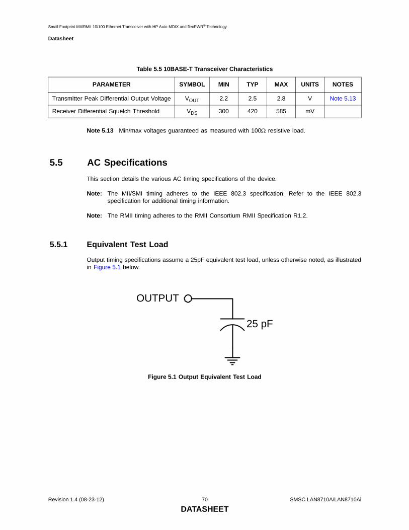
Small Footprint MII/RMII 10/100 Ethernet Transceiver with HP Auto-MDIX and flexPWR® Technology
Datasheet
Note 5.13 Min/max voltages guaranteed as measured with 100Ω resistive load.
5.5 AC SpecificationsThis section details the various AC timing specifications of the device.
Note: The MII/SMI timing adheres to the IEEE 802.3 specification. Refer to the IEEE 802.3specification for additional timing information.
Note: The RMII timing adheres to the RMII Consortium RMII Specification R1.2.
5.5.1 Equivalent Test Load
Output timing specifications assume a 25pF equivalent test load, unless otherwise noted, as illustratedin Figure 5.1 below.
Table 5.5 10BASE-T Transceiver Characteristics
PARAMETER SYMBOL MIN TYP MAX UNITS NOTES
Transmitter Peak Differential Output Voltage VOUT 2.2 2.5 2.8 V Note 5.13
Receiver Differential Squelch Threshold VDS 300 420 585 mV
Figure 5.1 Output Equivalent Test Load
25 pF
OUTPUT
Revision 1.4 (08-23-12) 70 SMSC LAN8710A/LAN8710Ai
DATASHEET

Small Footprint MII/RMII 10/100 Ethernet Transceiver with HP Auto-MDIX and flexPWR® Technology
Datasheet
5.5.2 Power Sequence Timing
This diagram illustrates the device power sequencing requirements. The VDDIO, VDD1A, VDD2A andmagnetics power supplies can turn on in any order provided they all reach operational levels withinthe specified time period tpon. Device power supplies can turn off in any order provided they all reach0 volts within the specified time period poff.
Note: When the internal regulator is disabled, a power-up sequencing relationship exists betweenVDDCR and the 3.3V power supply. For additional information refer to Section 3.7.4,"REGOFF: Internal +1.2V Regulator Configuration," on page 38.
Figure 5.2 Power Sequence Timing
Table 5.6 Power Sequence Timing Values
SYMBOL DESCRIPTION MIN TYP MAX UNITS
tpon Power supply turn on time 50 mS
tpoff Power supply turn off time 500 mS
VDDIO
Magnetics Power
tpon tpoff
VDD1A, VDD2A
SMSC LAN8710A/LAN8710Ai 71 Revision 1.4 (08-23-12)
DATASHEET

Small Footprint MII/RMII 10/100 Ethernet Transceiver with HP Auto-MDIX and flexPWR® Technology
Datasheet
5.5.3 Power-On nRST & Configuration Strap Timing
This diagram illustrates the nRST reset and configuration strap timing requirements in relation topower-on. A hardware reset (nRST assertion) is required following power-up. For proper operation,nRST must be asserted for no less than trstia. The nRST pin can be asserted at any time, but mustnot be deasserted before tpurstd after all external power supplies have reached 80% of their nominaloperating levels. In order for valid configuration strap values to be read at power-up, the tcss and tcshtiming constraints must be followed. Refer to Section 3.8.5, "Resets," on page 41 for additionalinformation.
Note: nRST deassertion must be monotonic.
Note: Device configuration straps are latched as a result of nRST assertion. Refer to Section 3.7,"Configuration Straps," on page 36 for details. Configuration straps must only be pulled high orlow and must not be driven as inputs.
Note 5.14 20 clock cycles for 25MHz, or 40 clock cycles for 50MHz.
Figure 5.3 Power-On nRST & Configuration Strap Timing
Table 5.7 Power-On nRST & Configuration Strap Timing Values
SYMBOL DESCRIPTION MIN TYP MAX UNITS
tpurstd External power supplies at 80% to nRST deassertion 25 mS
tpurstv External power supplies at 80% to nRST valid 0 nS
trstia nRST input assertion time 100 μS
tcss Configuration strap pins setup to nRST deassertion 200 nS
tcsh Configuration strap pins hold after nRST deassertion 1 nS
totaa Output tri-state after nRST assertion 50 nS
todad Output drive after nRST deassertion 2 800(Note 5.14)
nS
tcss
nRST
Configuration Strap Pins Input
trstia
tcsh
Configuration Strap Pins Output Drive
todad
All External Power Supplies tpurstd
80%
tpurstv
totaa
Revision 1.4 (08-23-12) 72 SMSC LAN8710A/LAN8710Ai
DATASHEET

Small Footprint MII/RMII 10/100 Ethernet Transceiver with HP Auto-MDIX and flexPWR® Technology
Datasheet
5.5.4 MII Interface Timing
This section specifies the MII interface transmit and receive timing. Please refer to Section 3.4.1, "MII,"on page 30 for additional details.
Note 5.15 40ns for 100BASE-TX operation, 400ns for 10BASE-T operation.
Note 5.16 Timing was designed for system load between 10 pf and 25 pf.
Figure 5.4 MII Receive Timing
Table 5.8 MII Receive Timing Values
SYMBOL DESCRIPTION MIN MAX UNITS NOTES
tclkp RXCLK period Note 5.15 ns
tclkh RXCLK high time tclkp*0.4 tclkp*0.6 ns
tclkl RXCLK low time tclkp*0.4 tclkp*0.6 ns
tval RXD[3:0], RXDV output valid from rising edge of RXCLK
28.0 ns Note 5.16
thold RXD[3:0], RXDV output hold from rising edge of RXCLK
10.0 ns Note 5.16
RXCLK
RXD[3:0]
RXDV
tclkh tclkl
tclkp
tval tholdtval
tval
thold
SMSC LAN8710A/LAN8710Ai 73 Revision 1.4 (08-23-12)
DATASHEET

Small Footprint MII/RMII 10/100 Ethernet Transceiver with HP Auto-MDIX and flexPWR® Technology
Datasheet
Note 5.17 40ns for 100BASE-TX operation, 400ns for 10BASE-T operation.
Note 5.18 Timing was designed for system load between 10 pf and 25 pf.
Figure 5.5 MII Transmit Timing
Table 5.9 MII Transmit Timing Values
SYMBOL DESCRIPTION MIN MAX UNITS NOTES
tclkp TXCLK period Note 5.17 ns
tclkh TXCLK high time tclkp*0.4 tclkp*0.6 ns
tclkl TXCLK low time tclkp*0.4 tclkp*0.6 ns
tsu TXD[3:0], TXEN setup time to rising edge of TXCLK
12.0 ns Note 5.18
thold TXD[3:0], TXEN hold time after rising edge of TXCLK
0 ns Note 5.18
TXCLKtsu
TXD[3:0]
TXEN
tclkh tclkl
tclkp
thold tsu thold thold
tsuthold
Revision 1.4 (08-23-12) 74 SMSC LAN8710A/LAN8710Ai
DATASHEET

Small Footprint MII/RMII 10/100 Ethernet Transceiver with HP Auto-MDIX and flexPWR® Technology
Datasheet
SMSC LAN8710A/LAN8710Ai 75 Revision 1.4 (08-23-12)
5.5.5 RMII Interface Timing
Note 5.19 Timing was designed for system load between 10 pf and 25 pf.
Figure 5.6 RMII Timing
Table 5.10 RMII Timing Values
SYMBOL DESCRIPTION MIN MAX UNITS NOTES
tclkp CLKIN period 20 ns
tclkh CLKIN high time tclkp*0.35 tclkp*0.65 ns
tclkl CLKIN low time tclkp*0.35 tclkp*0.65 ns
toval RXD[1:0], RXER, CRS_DV output valid from rising edge of CLKIN
14.0 ns Note 5.19
tohold RXD[1:0], RXER, CRS_DV output hold from rising edge of CLKIN
3.0 ns Note 5.19
tsu TXD[1:0], TXEN setup time to rising edge of CLKIN
4.0 ns Note 5.19
tihold TXD[1:0], TXEN input hold time after rising edge of CLKIN
1.5 ns Note 5.19
CLKIN(REF_CLK)
RXD[1:0], RXER
CRS_DV
tclkh tclkl
tclkp
toval toholdtoval
tovaltohold
tsu
TXD[1:0]
TXEN
tihold tsu tihold tihold
tsutihold
DATASHEET

Small Footprint MII/RMII 10/100 Ethernet Transceiver with HP Auto-MDIX and flexPWR® Technology
Datasheet
5.5.5.1 RMII CLKIN Requirements
5.5.6 SMI TimingThis section specifies the SMI timing of the device. Please refer to Section 3.5, "Serial ManagementInterface (SMI)," on page 33 for additional details.
Table 5.11 RMII CLKIN (REF_CLK) Timing Values
PARAMETER MIN TYP MAX UNITS NOTES
CLKIN frequency 50 MHz
CLKIN Frequency Drift ± 50 ppm
CLKIN Duty Cycle 40 60 %
CLKIN Jitter 150 psec p-p – not RMS
Figure 5.7 SMI Timing
Table 5.12 SMI Timing Values
SYMBOL DESCRIPTION MIN MAX UNITS NOTES
tclkp MDC period 400 ns
tclkh MDC high time 160 (80%) ns
tclkl MDC low time 160 (80%) ns
tvalMDIO (read from PHY) output valid from rising edge of MDC
300 ns
toholdMDIO (read from PHY) output hold from rising edge of MDC
0 ns
tsuMDIO (write to PHY) setup time to rising edge of MDC
10 ns
tiholdMDIO (write to PHY) input hold time after rising edge of MDC
10 ns
MDC
MDIO
tclkh tclkl
tclkp
tohold
MDIO
tsu tihold(Data-Out)
(Data-In)
tohold
tval
Revision 1.4 (08-23-12) 76 SMSC LAN8710A/LAN8710Ai
DATASHEET
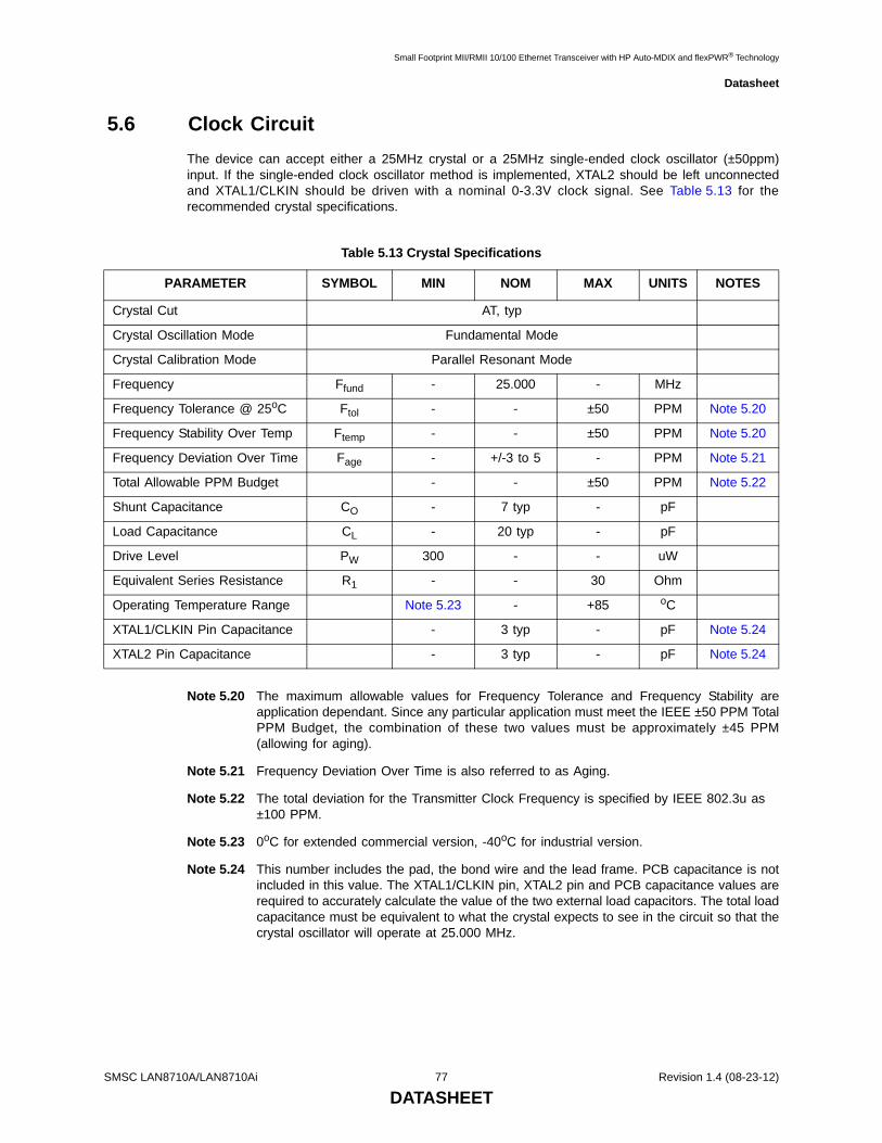
Small Footprint MII/RMII 10/100 Ethernet Transceiver with HP Auto-MDIX and flexPWR® Technology
Datasheet
5.6 Clock CircuitThe device can accept either a 25MHz crystal or a 25MHz single-ended clock oscillator (±50ppm)input. If the single-ended clock oscillator method is implemented, XTAL2 should be left unconnectedand XTAL1/CLKIN should be driven with a nominal 0-3.3V clock signal. See Table 5.13 for therecommended crystal specifications.
Note 5.20 The maximum allowable values for Frequency Tolerance and Frequency Stability areapplication dependant. Since any particular application must meet the IEEE ±50 PPM TotalPPM Budget, the combination of these two values must be approximately ±45 PPM(allowing for aging).
Note 5.21 Frequency Deviation Over Time is also referred to as Aging.
Note 5.22 The total deviation for the Transmitter Clock Frequency is specified by IEEE 802.3u as ±100 PPM.
Note 5.23 0oC for extended commercial version, -40oC for industrial version.
Note 5.24 This number includes the pad, the bond wire and the lead frame. PCB capacitance is notincluded in this value. The XTAL1/CLKIN pin, XTAL2 pin and PCB capacitance values arerequired to accurately calculate the value of the two external load capacitors. The total loadcapacitance must be equivalent to what the crystal expects to see in the circuit so that thecrystal oscillator will operate at 25.000 MHz.
Table 5.13 Crystal Specifications
PARAMETER SYMBOL MIN NOM MAX UNITS NOTES
Crystal Cut AT, typ
Crystal Oscillation Mode Fundamental Mode
Crystal Calibration Mode Parallel Resonant Mode
Frequency Ffund - 25.000 - MHz
Frequency Tolerance @ 25oC Ftol - - ±50 PPM Note 5.20
Frequency Stability Over Temp Ftemp - - ±50 PPM Note 5.20
Frequency Deviation Over Time Fage - +/-3 to 5 - PPM Note 5.21
Total Allowable PPM Budget - - ±50 PPM Note 5.22
Shunt Capacitance CO - 7 typ - pF
Load Capacitance CL - 20 typ - pF
Drive Level PW 300 - - uW
Equivalent Series Resistance R1 - - 30 Ohm
Operating Temperature Range Note 5.23 - +85 oC
XTAL1/CLKIN Pin Capacitance - 3 typ - pF Note 5.24
XTAL2 Pin Capacitance - 3 typ - pF Note 5.24
SMSC LAN8710A/LAN8710Ai 77 Revision 1.4 (08-23-12)
DATASHEET
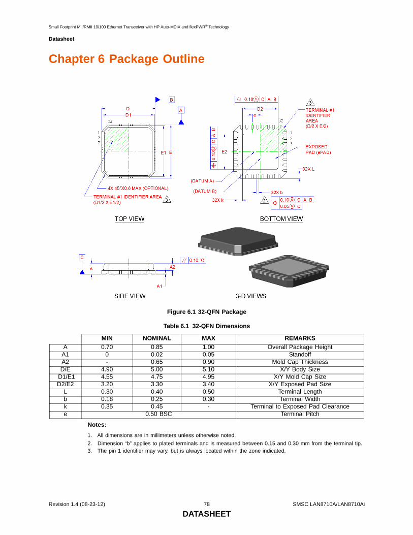
Small Footprint MII/RMII 10/100 Ethernet Transceiver with HP Auto-MDIX and flexPWR® Technology
Datasheet
Chapter 6 Package Outline
Notes:1. All dimensions are in millimeters unless otherwise noted.2. Dimension “b” applies to plated terminals and is measured between 0.15 and 0.30 mm from the terminal tip.3. The pin 1 identifier may vary, but is always located within the zone indicated.
Figure 6.1 32-QFN Package
Table 6.1 32-QFN Dimensions
MIN NOMINAL MAX REMARKSA 0.70 0.85 1.00 Overall Package Height
A1 0 0.02 0.05 StandoffA2 - 0.65 0.90 Mold Cap ThicknessD/E 4.90 5.00 5.10 X/Y Body Size
D1/E1 4.55 4.75 4.95 X/Y Mold Cap SizeD2/E2 3.20 3.30 3.40 X/Y Exposed Pad Size
L 0.30 0.40 0.50 Terminal Lengthb 0.18 0.25 0.30 Terminal Widthk 0.35 0.45 - Terminal to Exposed Pad Clearancee 0.50 BSC Terminal Pitch
Revision 1.4 (08-23-12) 78 SMSC LAN8710A/LAN8710Ai
DATASHEET

Small Footprint MII/RMII 10/100 Ethernet Transceiver with HP Auto-MDIX and flexPWR® Technology
Datasheet
Figure 6.2 Recommended PCB Land Pattern
Figure 6.3 Taping Dimensions and Part Orientation
SMSC LAN8710A/LAN8710Ai 79 Revision 1.4 (08-23-12)
DATASHEET
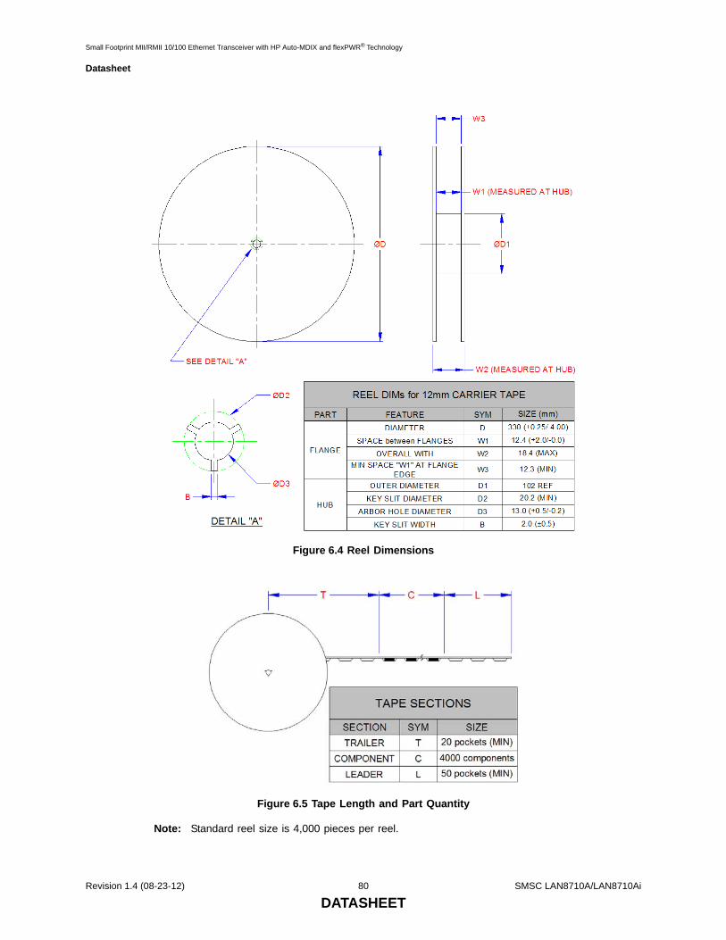
Small Footprint MII/RMII 10/100 Ethernet Transceiver with HP Auto-MDIX and flexPWR® Technology
Datasheet
Note: Standard reel size is 4,000 pieces per reel.
Figure 6.4 Reel Dimensions
Figure 6.5 Tape Length and Part Quantity
Revision 1.4 (08-23-12) 80 SMSC LAN8710A/LAN8710Ai
DATASHEET
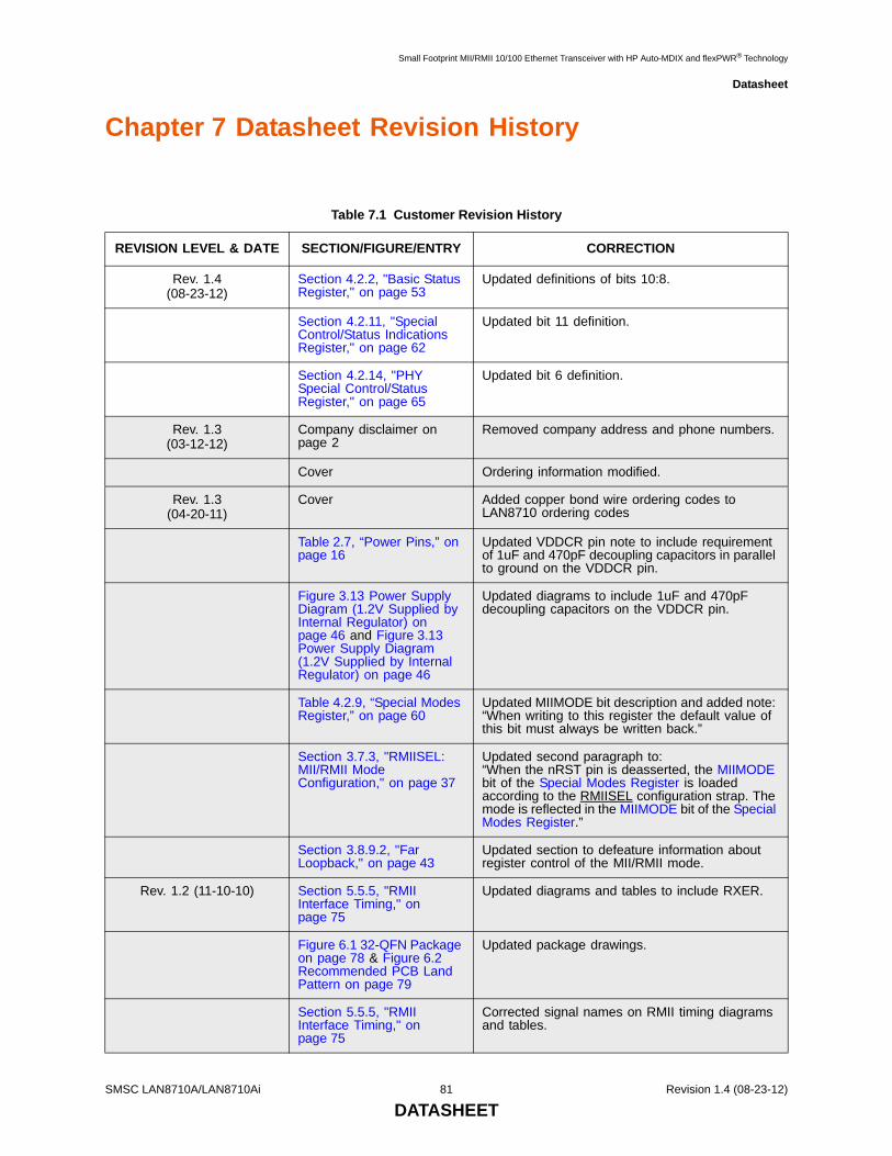
Small Footprint MII/RMII 10/100 Ethernet Transceiver with HP Auto-MDIX and flexPWR® Technology
Datasheet
Chapter 7 Datasheet Revision History
Table 7.1 Customer Revision History
REVISION LEVEL & DATE SECTION/FIGURE/ENTRY CORRECTION
Rev. 1.4(08-23-12)
Section 4.2.2, "Basic Status Register," on page 53
Updated definitions of bits 10:8.
Section 4.2.11, "Special Control/Status Indications Register," on page 62
Updated bit 11 definition.
Section 4.2.14, "PHY Special Control/Status Register," on page 65
Updated bit 6 definition.
Rev. 1.3(03-12-12)
Company disclaimer on page 2
Removed company address and phone numbers.
Cover Ordering information modified.
Rev. 1.3(04-20-11)
Cover Added copper bond wire ordering codes to LAN8710 ordering codes
Table 2.7, “Power Pins,” on page 16
Updated VDDCR pin note to include requirement of 1uF and 470pF decoupling capacitors in parallel to ground on the VDDCR pin.
Figure 3.13 Power Supply Diagram (1.2V Supplied by Internal Regulator) on page 46 and Figure 3.13 Power Supply Diagram (1.2V Supplied by Internal Regulator) on page 46
Updated diagrams to include 1uF and 470pF decoupling capacitors on the VDDCR pin.
Table 4.2.9, “Special Modes Register,” on page 60
Updated MIIMODE bit description and added note: “When writing to this register the default value of this bit must always be written back.”
Section 3.7.3, "RMIISEL: MII/RMII Mode Configuration," on page 37
Updated second paragraph to:“When the nRST pin is deasserted, the MIIMODE bit of the Special Modes Register is loaded according to the RMIISEL configuration strap. The mode is reflected in the MIIMODE bit of the Special Modes Register.”
Section 3.8.9.2, "Far Loopback," on page 43
Updated section to defeature information about register control of the MII/RMII mode.
Rev. 1.2 (11-10-10) Section 5.5.5, "RMII Interface Timing," on page 75
Updated diagrams and tables to include RXER.
Figure 6.1 32-QFN Package on page 78 & Figure 6.2 Recommended PCB Land Pattern on page 79
Updated package drawings.
Section 5.5.5, "RMII Interface Timing," on page 75
Corrected signal names on RMII timing diagrams and tables.
SMSC LAN8710A/LAN8710Ai 81 Revision 1.4 (08-23-12)
DATASHEET

Small Footprint MII/RMII 10/100 Ethernet Transceiver with HP Auto-MDIX and flexPWR® Technology
Datasheet
Section 5.5.4, "MII Interface Timing," on page 73
Corrected signal names on MII timing diagrams and tables. Updated Table 5.8 tval max to 28.0 ns. Updated Table 5.9 tsu and thold values to 12.0 ns and 0 ns, respectively.
Table 5.7, “Power-On nRST & Configuration Strap Timing Values,” on page 72
Updated todad description: “Output drive after nRST deassertion”
Rev. 1.1 (04-09-10) Section 5.1, "Absolute Maximum Ratings*"
Modified “HBM ESD Performance by adding “per JEDEC JESD22-A114” and changed “+/-5kV” to “Class 3A”
Section 5.3, "Power Consumption," on page 67
Corrected typo in the current consumption table row title: “100BASE-TX /W TRAFFIC”
Section 5.3, "Power Consumption," on page 67
Corrected typo in note regarding Ethernet component current: “The Ethernet component current is typically 41mA in 100BASE-TX mode and 100mA in 10BASE-T mode, independent of the 2.5V or 3.3V supply rail of the transformer.”
Table 5.2, “Non-Variable I/O Buffer Characteristics,” on page 68
Corrected O12 VOH minimum value to “VDD2A - 0.4”Corrected ICLK VILI maximum value to “0.35”Corrected ICLK VIHI maximum value to “VDD2A + 0.4”
Section 5.2, "Operating Conditions**," on page 67
Added note: “Do not drive input signals without power supplied to the device.”
Section 5.1, "Absolute Maximum Ratings*," on page 66
Corrected IEC61000-4-2 Contact Discharge ESD Performance to +/-8kV.
Section 4.2.4, "PHY Identifier 2 Register," on page 55
Corrected Model Number default value to “001111b”.
Section 3.8.9.2, "Far Loopback," on page 43
Added far loopback description.
Section 4.2.8, "Mode Control/Status Register," on page 59
Added FARLOOPBACK (bit 9) description.
Table 5.9, “MII Transmit Timing Values,” on page 74
Corrected tsu and thold minimum values to 10 ns.
Rev. 1.0 (12-09-09) Document reworked for clarity and consistency with other SMSC documentation.
Rev. 1.0 (04-15-09) Initial Release
Table 7.1 Customer Revision History (continued)
REVISION LEVEL & DATE SECTION/FIGURE/ENTRY CORRECTION
Revision 1.4 (08-23-12) 82 SMSC LAN8710A/LAN8710Ai
DATASHEET