Embed Size (px)
Citation preview

1
LABORATORY MANUAL ELECTRICAL MEASUREMENTS
and Circuits EE 2049
Khosrow Rad 2016
DEPARTMENT OF ELECTRICAL & COMPUTER ENGINEERING
CALIFORNIA STATE UNIVERSITY, LOS ANGELES Published July 13, 2016

2
CONTENTS Experiment Title Page
1 Digital Multimeter Resistance Measurement 3
2 Digital Multimeter: DC Voltage and DC Current Measurement 5
3 Voltage Regulation and AC Power Supply 7
4 Function Generator and Oscilloscope 9
5 Oscilloscope Operation 12
6 PSpice Analysis of DC Circuits 15
7 Basic Circuit and Divider Rules 18
8 Kirchhof's Voltage Law and Kirchhof's Current Law 20
9 Divider rules for voltage (VDR) and current (CDR). 23
10 Mesh & Nodal Analysis 26
11 Thévenin’s Theorem 29
12 PSpice: Time Domain Analysis 33
13 The Response of an RC Circuit 39
14 The Response of an RL Circuit 42
15 Series Resonant Circuit 46
16 The Complete Response of 2nd Order RLC Circuits 49

3
Digital Multimeter Resistance Measurement EXPERIMENT 1
Here is the resistor color code:
Color First Stripe Second Stripe Third Stripe Fourth Stripe Black 0 0 x1 Brown 1 1 x10 Red 2 2 x100 Orange 3 3 x1,000 Yellow 4 4 x10,000 Green 5 5 x100,000 Blue 6 6 x1,000,000 Purple 7 7 Gray 8 8 White 9 9 Gold 5% Silver
10% None 20%
If the following color comes in third stripe it will act as Gold = * decimal multiplier =10-1 = 0.1 tolerance Silver = * decimal multiplier =10-2 = 0.01 tolerance No color = * decimal multiplier = * tolerance 1. Obtain about 15 resistors of the 15 KΩ value. Measure the resistance of each resistor using the DMM range that will give the maximum number of significant figures. Draw a distribution graph with the vertical axis being the number of resistors within each 1 % range and the horizontal axis being the percent deviation from the nominal resistance value. Make you table for all 15 resister same as table 1.

4
2. Obtain a Resistance Substitution Box and use a DMM to measure the resistance values for all of the resistance settings to the maximum number of significant figures. Compare the actual resistance values to the nominal values in terms of the percent difference.
3. Connect short lead or jumper wire using your red and black wire between the DMM input terminals and read the resistance, using the lowest resistance range to obtain the maximum number of significant figures. Now connect long lead wire to the DMM and repeat the measurement. Calculate the approximate values of resistance per foot of the lead wire. Use the DMM NULL for an easier measurement of this.
4. Variable Resistors: Obtain a 5000 Ω variable resistor (potentiometer or rheostat). a) Measure the total (i.e. end-to-end) resistance. b) Measure the resistance between the "wiper arm” and one end with the knob in the fully clockwise position, and then with the knob in the fully counter-clockwise position. Then repeat this for the resistance between the wiper arm and the other end of the resistor.
5. In some cases, especially when using the DMM to measure resistance values associated with various electronic devices, it is important to know the voltage produced by the DMM when measuring resistance. Connect the DMM to a resistance substitution box and for every DMM resistance range adjust the resistance to give a reading as close to the full-scale resistance reading as possible. Connect a second DMM set to read voltage across (in parallel with) the first DMM and reading the test voltage of the first DMM.
6. OUESTIONS: a) Give the color codes for the following resistors:
i) 2 Ω, 5% ii) 0. Ω, 5% iii) 1 k Ω, 20%
b) The highest resistance range on a DMM is 20 MΩ. To measure a very large unknown resistor Rx, the unknown resistor is placed in parallel with a resistor that has previously been measured and has an actual value of 19.95 M Ω. The resulting DMM reading is 18.16 MΩ. Find the value of Rx

5
DIGITAL MULTIMETER: D-C VOLTAGE and D-C Current MEASUREMENT EXPERIMENT 2 1. Connect the Digital Multimeter (DMM) to a DC Power Supply as show in Figure below . Set the DMM to read DC VOLTS.
2. Connect a Resistance Substitution Box in series between the DC Power Supply and the DMM. Set the resistance value to a low setting of 1 KΩ. Carefully adjust the DC Power Supply to give a reading of 10V on the DMM. Now read the DMM for the following values of series resistance: 10 MΩ, 4.7 MΩ, 1 MΩ, and 100 KΩ.
From these readings, use voltage division to calculate R Vi, the equivalent internal resistance of the voltmeter.
3. QUESTIONS: a) Define "resolution", "accuracy", and "precision" and explain the differences (if any) among these three terms. b) What is the difference between the "nominal" and the "actual" value of an electronic component?
Measure DC resistance of the DMM Ammeter: Ammeters also have an internal electrical resistance. Ideally an ammeter would have no resistance (0 Ω) so that it would not alter the current flow it is trying to measure. In this exercise you will measure the DC resistance of the real DMM ammeter. Set up the circuit as shown in Figure 2. Using the DMM for the ammeter

6
Figure 2
Set the resistor R to 1 MΩ resistance. And record the resistance R and the current indicated by the ammeter. f. Adjust R to 100kΩ. In your table, record the resistance R and the current indicated by the ammeter. g. Continue to decrease the resistance R until the ammeter reading drops by a significant fraction (up to about one half) of the original value. Record the final resistance R and measured current. Use the DMM ohmmeter to measure the actual final resistance R, rather than relying on the indicated settings of the substitution box. (You will need to connect the DMM cables to “VΩ” and “COM” for this measurement.) i. From these readings, use current division to calculate RAi, the equivalent internal resistance of the ammeter. 5. Questions
a) What is the input resistance of an ideal current-measuring DMM? b) What is the input resistance of an ideal voltage-measuring DMM? c) How must a DMM be connected in a circuit to measure current: In series or in parallel? d) How must a DMM be connected in a circuit to measure voltage: In series or in parallel? e) Under what conditions will the voltage burden or the input resistance of the DMM produce a significant
error in current measurement?

7
Voltage Regulation and AC Power Supply EXPERIMENT 3
A. VOLTAGE REGULATION
1. Connect the DC Power Supply to the Digital Multimeter (DMM) and set the DC Power Supply to give an output voltage of 10V as read on the DMM. Read and record the DC voltage to the maximum number of significant figures.
2. Connect a 50 Ω, 10 watt resistor across the DC Power Supply. Record the new value of the voltage. (Use the NULL for an easier measurement.)
3. Calculate the voltage regulation of the DC Power Supply as defined by
voltage regulation = (no-load voltage) - (full-load voltage/ (no-load voltage) x 100%
The no-load voltage is the output voltage of the DC Power Supply when the output current is zero. The full-load voltage in this case is the output voltage when the output current is 10V/50 Ω = 200 mA.
4. Calculate the output resistance R0 of the DC Power Supply from the relationship
R0 = (no-load voltage) - (full-load voltage) / (full-load current) - (no-load current) AC
RIPPLE FACTOR
5. Set the DMM to read AC voltage. Read and record the AC voltage (in millivolts). Do this for both the full-load (50 Ω) and the no-load conditions. Calculate the DC Power Supply ripple factor as given by
Ripple factor = AC Ripple Voltage / DC Output Voltage x 100%
6. QUESTIONS:
a) What does a DC Power Supply do? b) Why is there an AC ripple present, and will a battery have an AC ripple? c) If a DC Power Supply has an output resistance of 10 mΩ (milli-ohms) and a no-load output voltage of 10V, find the change in the output voltage and the load regulation for a full-load output current of 1 A. d) A DC Power Supply is adjusted to give a no-load output voltage 10V. The AC line voltage is 115V RMS. When a full-load current of 1 A is drawn, the output voltage drops to 9.98V. Find the no-load to full-load load regulation expressed in percent. e) When the AC line voltage drops from 11 5V to 110V, the DC output voltage decreases from 10V to 9.95V. Find the line regulation expressed in terms of %/V.
f) If the DC output voltage is 10V and RMS AC ripple voltage on the output is 10 mV, find the percentage ripple factor.

8
g) As the temperature varies from 25 °C to 35 °C, the output voltage increases from 10V to 10.05V. Find the temperature coefficient of the output voltage expressed. B. AC Power Supply
Connect a Digital Multimeter (DMM) to a FUNCTION GENERATOR. Set the DMM function control to read AC voltage. Adjust the frequency control of the FUNCTION GENERATOR to 1 kHz. Adjust the amplitude control to give an output voltage of 1V RMS as read on the DMM. Compare the volts peak-to-peak (VPP) reading on the FUNCTION GENERATOR to the DMM reading. Are they consistent? 1. Increase the frequency up to the point where the DMM reading has changed by about 10%.
2. Now reduce the frequency of the Function Generator to below 1 kHz, and decrease the frequency to the point
where the DMM reading has changed by about 10%. 3. DMM Input Impedance
Set the FUNCTION GENERATOR frequency to 100 Hz and adjust the output voltage to 1V RMS. Connect a 1 MΩ resistor in series between the FUNCTION GENERATOR and the DMM. Now increase the frequency 100 kHz. Read the DMM, and from the reading calculate the DMM input capacitance.

9
FUNCTION GENERATOR and OSCILLLOSCOPE EXPERIMENT 4 1. a) Connect a Digital Multimeter to the Function Generator. Connect a fixed resistor across (i.e. in parallel with) the output of the Function Generator. Set the frequency to 1 kHz and the output voltage to 1.0 V. Change the resistance until the output voltage is down to about one-half of its original value. Record the voltage and resistance values.
2. Calculate the output resistance of the Function Generator. Compare with the specifications.
3. What value of output resistance would the "ideal" Function Generator have? Explain.
4. QUESTIONS
a) A Function Generator is adjusted to give a no-load (open-circuit) voltage of 1.0V. When a 1 K Ω
load is placed across the output terminals of the Function Generator the output voltage drops to 0.8 V. Find the output resistance of the Function Generator.
Voltage Ratio in decibels (dB) = 20 log10 (V1/V2)
b) Express the following ratios in decibels (dB): i) V1/V2 =100 ii) V1/V2 = 0.1
c) Change these dB values to voltage ratios i) -10dB
ii) 3dB d) A Function Generator has a specification that the variation in the output voltage with frequency will remain
flat to within ± 1 dB over the frequency range of 10 Hz to 100 kHz. Find the corresponding maximum percentage variation in the output voltage over this frequency range.
B. OSCILLLOSCOPE
Connect the Function Generator main output to the Channel 1 input of the oscilloscope and to a DMM (all in parallel). Connect the Function Generator sync (synchronization) output to the Channel 2 input of the oscilloscope.
1. Set the Function Generator to give a sine wave output at a frequency = 1 kHz. Adjust the amplitude to give a peak-to-peak voltage of 2V as observed on the oscilloscope. Press the Autoscale button on oscilloscope for the initial settings. Import oscilloscope display to computer. Then display only the sine wave on Channel 1.
a) Import oscilloscope display to computer
b) Compare the peak-to-peak voltage as measured by counting divisions and using the voltage/DIV scale
to that obtained from the oscilloscope direct voltage measurement.
10
c) Record the RMS voltage as observed on the DMM. Compare that to the RMS voltage as measured by the oscilloscope.
d) Compare the RMS voltage with the expected value based on the peak-to-peak voltage.
e) Measure the period of the waveform by counting divisions and using the time/DIV scale. Find the
frequency and compare to the expected value.
f) Obtain the period of the waveform using the oscilloscope direct measurement. Compare to the value obtained by counting divisions and using the time/DIV scale.
g) Obtain the frequency of the waveform using the oscilloscope direct measurement. Compare with the
value set on the Function Generator.
2. Set the Function Generator to give a square wave output at a frequency = 1 kHz with an amplitude of 2V peak-to-peak voltage as observed on the oscilloscope.
h) Import oscilloscope display to computer
i) Compare the peak-to-peak voltage as measured by counting divisions and using the voltage/DIV scale
to that obtained from the oscilloscope direct voltage measurement.
j) Record the RMS voltage as observed on the DMM. Compare that to the RMS voltage as measured by the oscilloscope.
k) Compare the RMS voltage with the expected value based on the peak-to-peak voltage.
l) Measure the period of the waveform by counting divisions and using the time/DIV scale. Find the frequency and compare to the expected value.
m) Obtain the period of the waveform using the oscilloscope direct measurement. Compare to the value
obtained by counting divisions and using the time/DIV scale.
n) Obtain the frequency of the waveform using the oscilloscope direct measurement. Compare with the value set on the Function Generator.
3. Set the Function Generator to give a square wave output at a frequency = 1 kHz with an amplitude of 2V peak-to-peak voltage as observed on the oscilloscope.
a) Import oscilloscope display to computer
b) Compare the peak-to-peak voltage as measured by counting divisions and using the voltage/DIV scale
to that obtained from the oscilloscope direct voltage measurement.
c) Record the RMS voltage as observed on the DMM. Compare that to the RMS voltage as measured by the oscilloscope.

11
d) Compare the RMS voltage with the expected value based on the peak-to-peak voltage.
e) Measure the period of the waveform by counting divisions and using the time/DIV scale. Find the
frequency and compare to the expected value.
f) Obtain the period of the waveform using the oscilloscope direct measurement. Compare to the value obtained by counting divisions and using the time/DIV scale.
g) Obtain the frequency of the waveform using the oscilloscope direct measurement. Compare with the
value set on the Function Generator.
4.Set the DMM to read DC volts. Turn on the DC OFFSET control on the Function Generator and rotate it to give a DC offset of +1V. Measure the shift in the DC level on the oscilloscope and compare with the value of DC voltage indicated by the DMM. Set the DMM to read AC volts. What is the change in the DMM AC voltage reading as the DC offset is changed from zero to +1V?
5.Repeat the previous procedure with a DC offset of -1V.
6..Change the input coupling switch to AC and now observe what happens 7.Set the Function Generator back to a SINE WAVE output. Change the Trigger slope to NEGATIVE SLOPE and observe what happens. Now change the TRIGGER SLOPE to POSITIVE SLOPE and observe the result.
7.Change the sweep speed control (TlME/DlV) to 0.5ms/DIV. Measure the period and compare with the previous result.
8.Repeat the previous procedure for sweep speeds (TIME/DIV) of 1.0 ms/DIV, 2.0 ms/DIV, and 0.1 ms/DIV.
9.Set sweep speed to 1 ms/DIV. Measure the period for the following frequencies and compare with the expected values: 2 kHz, 4 kHz, and 10 kHz.

12
OSCILLOSCOPE OPERATION EXPERIMENT 5 A. X-Y DISPLAY 1. Set up the oscilloscope for an X-Y display. Connect one Function Generator to the CH 1 input to be displayed on the Y- axis, and a second Function Generator to the CH 2 input to be displayed on the X-axis. Set the frequency of the second Function Generator to 100 Hz. Set the output voltage level of the second Function Generator to give a peak-to-peak voltage of 6V.
2. Adjust both Function Generators to produce a circle on the screen with a diameter of 6V. Sketch and dimension the display and record the Function Generator settings.
3. Adjust both Function Generators to produce an ellipse on the screen with a major axis (X-axis) of 6V and a minor axis (Y-axis) of 2V. Sketch and dimension the display and record the Function Generator settings.
4. Adjust both Function Generators to produce a diamond-shaped figure on the screen with a major axis (X-axis) of 6V and a minor axis (Y-axis) of 6V. Sketch and dimension the display and record the Function Generator settings.
5. Adjust both Function Generators to produce a diamond-shaped figure on the screen with a major axis (X-axis) of 6V and a minor axis (Y-axis) of 2V. Sketch and dimension the display and record the Function Generator settings.
6. Adjust both Function Generators to produce a diamond-shaped figure on the screen with a major axis (X-axis) of 2V and a minor axis (Y-axis) of 6V. Sketch and dimension the display and record the Function Generator settings.
7. Adjust both Function Generators to produce a pattern of dots on the screen with a spacing of 4V between dots in both directions. Sketch and dimension the display and record the Function Generator settings.
8. Adjust both Function Generators to produce a "figure 8" pattern on the screen with the "figure 8" being 6V high and 4V wide. Sketch and dimension the display and record the function Generator settings.
9. Adjust both Function Generators to produce a horizontal (i.e. sideways) "figure 8" pattern on the screen with the "figure 8" being 4V high and 8V wide. Sketch and dimension the display and record the Function Generator settings.
B. OSCILLOSCOPE DUAL CHANNEL DISPLAY 1. Connect a Function Generator to both the CH 1 and CH 2 Input terminals of the oscilloscope. Set input coupling switches to DC for both channels. Set the Function Generator to give a SQUARE WAVE output voltage waveform with a peak-to-peak amplitude of 5V and a frequency of 10 kHz. The oscilloscope sweep speed should be set to 10 µs/DIV. Adjust the vertical controls of both channels such that the two displays overlap exactly.
Oscilloscope Dual Channel Operation 2. Now insert an R-C low-pass network between the Function Generator and the CH 2 input of the oscilloscope.

13
The RC network consists of a Resistance Substitution Box (R1) and a Decade Capacitor Box, Type CDA (C1) as shown in the diagram below. Start off with the resistance set to 10 KΩ and the capacitance set to zero. The input -voltage of the R-C network is displayed on CH 1 and the output voltage will be displayed by CH2.
Measurement of the Time Domain Response Characteristics
3. Increase the capacitance and observe the results on the oscilloscope. Find the time it takes the output voltage to go from zero to 63.2% of the input voltage for four different values of capacitance. Decrease the frequency as necessary to display the full transient response curve. Compare the zero to 63.2% rise time with the R-C time constant (i.e. the R-C product). Repeat this procedure for the 100% to 36.8% faIl time.
4. Set the resistance to zero and the capacitance to 1 nF (0.001 µF). Now increase the resistance and observe the results on the oscilloscope. Decrease the frequency as necessary to display the full transient response curve. Find the time it takes the output voltage to go from zero to 63.2% of the input voltage for four different values of resistance. Compare the zero to 63.2% rise time with the R-C time constant. Repeat this procedure for the 100% to 36.8% fall time.
5. Set the resistance to 10 KΩ and the capacitance to 0.001 µF. vary the frequency of the Function Generator from about 100 Hz to about 1 MHz and observe the results. Find the frequency at which the output voltage reaches only 10% of the input voltage. Under these conditions the pulse width should be approximately equal to 1/10 of the R-C time constant. Compare the time constant to the pulse width.
6. Set the Function Generator to produce a SINE WAVE output. Set R1 to 10 KΩ and C1 to 0.001 µF. vary the frequency of the Function Generator from about 100 Hz up to about 2 MHz and compare the input and output waveforms.
7. Find the frequency at which the output voltage has decreased to 70.71 % of the input voltage. Find the phase angle between the output and input waveforms at this frequency. Compare the frequency and phase angle with the expected values. Repeat this procedure for the frequency at which the output voltage has decreased to 50% of the input voltage, and then for the frequency at which the output voltage is only 10% of the input voltage.
8. QUESTIONS
For most electronic systems the relationship between the 3 dB bandwidth (BW) and the rise time (10% to 90%) is given approximately by RISE TIME x BW = 0.35.
Note: If a signal passes through several systems in series, (i.e. cascaded) the rise time at the output is given approximately as the square root of the sum of the squares of the rise times of the individual systems.
a) An oscilloscope has a 35 MHz BW. Find the apparent rise time of the oscilloscope display if the signal input to the oscilloscope is an ideal pulse waveform. b) An oscilloscope has a 35 MHz BW. The oscilloscope is connected directly to a Pulse Generator and the oscilloscope display shows a rise time of 15 ns. Find the rise time of the Pulse Generator

14
output. c) A Pulse Generator produces a pulse waveform output with a 10 ns rise time. After the pulse signal has passed through some electronic system it is displayed on the screen of a 35 MHz oscilloscope. The oscilloscope display shows a rise time of 25 ns. Find the rise time and the 3 dB BW of the electronic system. d) The input voltage of a system is displayed on CH 1 of an oscilloscope and the output voltage is displayed on CH 2. Both waveforms are sinusoidal with a period of 1 ms. The CH 2 waveform lags behind the CH 1 waveform by 0.1 ms. Find the phase shift produced by the system under study. Express the answer in degrees and in radians
PSpice Analysis of DC Circuits EXPERIMENT 6

15
OBJECTIVES Use PSpice Circuit Simulator to check laboratory circuits and homework problems
EQUIPMENT PSpice Program
THEORY A dc circuit is a circuit in which the voltages of all independent voltage sources and the currents of all independent current sources have constant values. All of the currents and voltages of a dc circuit, including mesh currents and node voltages, have constant values. PSpice can analyze a dc circuit to determine the values of the node voltages and also the values of the currents in voltage sources. PSpice uses the name “Bias Point” to describe this type of analysis. The name “Bias Point” refers to the role of dc analysis in the analysis of a transistor amplifier.)
In this lab we consider four examples. The first example illustrates analysis of circuits containing independent sources while the second is dependent sources. The third illustrates the use of PSpice to check the node or mesh equations of a circuit to verify that these equations are correct. The final example uses PSpice to compare two dc circuits.
There is a six-step procedure to organize circuit analysis using PSpice. This procedure is stated as follows: Step 1. Formulate a circuit analysis problem. Step 2. Describe the circuit using Schematics. This description requires three activities.
a. Place the circuit elements in the Schematics workspace. b. Adjust the values of the circuit element parameters. c. Wire the circuit to connect the circuit elements and add a ground.
Step 3. Simulate the circuit using PSpice. Step 4. Display the results of the simulation, for example, using probe. Step 5. Verify that the simulation results are correct. Step 6. Report the answer to the circuit analysis problem.
Part 1: DC Circuits Containing Independent Sources Part 1A: Capturing and Simulating the DC Circuit Apply the six-step procedure to analyze the circuit shown to determine the value of v6, the voltage across the 6Ω resistor.
PSpice Circuit
Part 1B: Verify that the simulation results are correct
0
20.00V
I12A
R26
0V
V124V
V6
-
+
R1 3
24.00V

16
Use simple circuit methods to verify the results. Is the original circuit equivalent to the PSpice circuits? Use short concise sentences to explain your reasoning.
Part 2: DC Circuits Containing Dependent Sources PSpice can be used to analyze circuits that contain dependent sources. The PSpice symbols used to represent dependent sources are labeled as E, F, G and H (see table to the right) and are located in the analogy library.
Part 2A: Capturing and Simulate a CCCS Circuit This example illustrates analysis of a circuit that contains a dependent source. Particular attention is paid to preparing the circuit for analysis using PSpice. Suppose that a circuit containing a dependent source is
An equivalent PSpice circuit would look like
Part 2B: Verify that the simulation results are correct Use simple circuit methods (hint: KCL at each node) to verify the results of v and i. Are the two circuits’ equivalent?
Part 3: Mesh and Node Equations In this example, PSpice is used to check node and mesh equations of a circuit. Consider the circuit shown. A set of mesh currents has been labeled and the nodes of this circuit have been numbered. The circuit can be represented by the following node and mesh equations:
b c
b c d
c d
23v 12v 36
55v 21v 6v 0
6v 26v 180
− =
− + − =
− + =
1 2 3 4
1 2 3
1 2 3 4
2 3 4
17i 8i 2i 5i 0
8i 11i 3i 12
7i 3i 5i 11i 0
4i 3i i 0
− − − =
− + − =
− − + + =
− + + =
Node equations Mesh equations
The objective of this example is to use PSpice to determine if these equations are correct.

17
Part 3A: Formulating a circuit with PSpice
We have seen that PSpice will calculate the node voltages of a circuit such as the one shown above. The node equations can be checked by determining the values of the node voltages using PSpice and substituting those values into the node equations. PSpice does not calculate mesh currents, but it does calculate the currents in voltage sources. The mesh current i2 is the current through the 12 V voltage source. PSpice uses the passive convention for all elements, including voltage sources. The voltage source current that PSpice will report is the current direction from + to −. In this case, PSpice will report the value of –i2 rather than i2. Similarly, 0V-voltage sources can be added to the circuit to measure the other mesh currents such as mesh currents i1, i3 and i4.
Part 3B: Verify that the simulation results are correct One can verify the results by one of the following ways. (i) Substitute the node voltages (mesh currents) from PSpice into the node equations (loop equations) and verify that they satisfy these equations. (ii) Solve the system of equations (for both Node and Mesh) using the matrix operations on your calculator and compare them to the PSpice results.
Part 4: Challenge PSpice Circuit A dc circuit with dependent sources is shown. Use PSpice to find the values of ix, iy and vz.
What to turn in: turn in all PSpice circuits for each of the parts listed below.
Part 1: Determine the voltage v across the 6Ω-resistor using simple circuit techniques and compare it to PSpice calculated value. How do they compare? Part 2: Determine the voltage v across the 5Ω-resistor and the current i through the 6Ω-resistor using simple circuit techniques and compare it to PSpice calculated values. How do they compare? Part 3: Use PSpice to determine the node voltages (vb, vc, vd) and the mesh (or loop) currents (i1, i2, i3, i4). Substitute these values into the node equations and the mesh equations. Do the PSpice values satisfy these node and mesh equations? Part 4: Use PSpice to determine that the controlling variables (ix, iy, vz) and verify that the dependent source values are correct.

18
Basic Circuit and Divider Rules EXPERIMENT 7 Part 1 Basic Circuit OBJECTIVES
1. Become familiar and organized Circuit Kit for the semester. 2. Become familiar with a breadboard with the lab power supply and review the measurement of voltage, current,
and resistance using a Digital Multimeter (DMM).
EQUIPMENT Power supply
Part 1: Connection Pattern of the Breadboard a. Set the DMM to OHMS and the range to lowest resistance. Use jumper wires to make connections to the
meter. Measure the continuity between different sets of pins to determine which groups of pins are connected and which are not. Lack of continuity will be read as an open circuit by the DMM.
b. Set the power supply to 10V and connect it to the breadboard posts. Use jumper cables to transfer the power from the posts to the breadboard pins labeled “+” and “−” at the top of the board. Measure the open-circuit voltages to confirm that the power was transferred.
Part 2: Basic Series Measurements Construct the circuit
a. Calculate the theoretical equivalent series resistance RS,thy using the measured resistor values. b. Measure the experimental equivalent series resistance RS,expt using a DMM. Use a percent difference to compare
the theoretical and experimental values. How do they compare? c. Energize the circuit and measure the current using an ammeter. d. Using the supply voltage and the ammeter reading, calculate the equivalent series resistance RS,Ohm using Ohm’s
law. Use a percent difference to compare the RS,Ohm with RS,expt from part (2b). How do they compare? e. Repeat parts (2a-2d) where the voltage has been increased to 30V.

19
Part 3: Basic Parallel Measurements Construct the circuit
a. Calculate the theoretical equivalent parallel resistance RP,thy using the measured resistor values. b. Measure the experimental equivalent parallel resistance RP,expt using a DMM. Use a percent difference to
compare the theoretical and experimental values. How do they compare? c. Energize the circuit and measure the current using an ammeter. d. Using the supply voltage and the ammeter reading, calculate the equivalent parallel resistance RP,Ohm using
Ohm’s law. Use a percent difference to compare the RP,Ohm with RP,expt from part (3b). How do they compare?

20
Kirchhof's Voltage Law and Kirchhof's Current Law EXPERIMENT 8 1. Obtain 6 randomly selected resistors with values between 1.0 Kohm and 10 Kohms. Measure the actual resistance values with a Digital Multimeter (DMM). The resistance range on the DMM should be chosen so as to obtain the maximum accuracy (i.e. maximum number of digits for the DMM reading). Compare the actual resistance values as determined by the DMM with the nominal resistance value as obtained from the color bands on the resistor. Determine If the actual resistance values are within the tolerance limits for each resistor. 2. Construct the circuit shown in Figure 8.1.1. Adjust the supply voltages Vs to +10 Volts.
Figure 8.1.1
3. Measure all branch voltages with a DMM. The measurements should be made with the DMM range chosen so as to obtain maximum accuracy (i.e. maximum number of digits) for each branch voltage measurement. Remember to keep proper track of the algebraic signs. 4. Verify that Kirchhof's Voltage Law is satisfied for all of the loops in the circuit. Measure all branch voltages in the circuit with a DMM, Do they add (algebraically) to zero ? Calculate the percentage error based on the following equation:
percentage error = ∑ V / [ (1/2) ∑ |V| ] x 100 % Does the percentage error obtained seem reasonable in view of the accuracy of the DMM ? 5. From the branch voltages calculate the branch currents. Remember to use the actual, and not the nominal resistance values for this calculation, Verify that Kirchhof's Current Law is satisfied at every node in the circuit. Calculate the percentage error using the relationship:
percentage error = ∑ I / [ (1/2) ∑| I | ] •100 % Does the percentage error obtained seem reasonable In view of the accuracy of the DMM ? 6. Using network reduction calculate the expected values of all of the branch currents. Compare the branch current values so obtained with the values obtained by the DMM measurements (in step 5). 7.The input resistance of the DMM is 10 Mohms. How much error will this input resistance result in? Will the

21
loading effect of the DMM input resistance account for some of the experimental error in steps 4 and 8.2 SUPERPOSITION THEOREM 1. Using the same circuit as for experiment 1, insert an additional power supply into the last loop as shown in Figure 8.2.1.
Figure 8.2.1
Set V1 to +10 V and V2 to +15 V. Double check the values of V1 and V2. 2. Measure all branch voltages with a DMM (maximum place accuracy), Remember to keep track of algebraic signs. 3. Replace V2 by a short-circuit. Measure all branch voltages. Then put V2 back into the circuit. 4. Replace V1 by a short-circuit. Measure all branch voltages. 5. From the above measurements verify that the superposition theorem is satisfied. 6. Using network reduction and the superposition theorem calculate the expected values of all of the branch voltages in the circuit. Compare the calculated values with the measured values.

22
8.3 THEVENIN’S THEOREM 1. Set up the circuit shown in Figure 8.3.1 using the same resistor network as used in experiment 1. Adjust VS to +10V. For RL use a resistance substitution box.
Figure 8.3.1
2. Measure the output voltage VO for the following values of load resistance RL (ohms): 1K, 10K, 33K, and 100K. Measure VO with the maximum number of significant digits on the DMM. 3. Replace RL by a short-circuit. Measure the voltage drop across R6 and calculate the short-circuit current from ISC=VR6/R6. 4. Disconnect RL from the circuit and measure the open-circuit output voltage VO=VOC. 5. With RL still out of the circuit, replace VS by a short-circuit. Measure the resistance RO that is seen looking back into the circuit using a DMM. Verify that RO=VOC/ISC. 6. Construct the Thevenin equivalent circuit using a resistance decade box for RO. Use a DMM for the adjustment of the resistance value of the resistance decade box so that it will be equal to RO. 7. Connect the load resistance RL to the Thevenin equivalent circuit. Measure the output voltage VO for the following values of load resistance RL (ohms): 1K, 10K, 33K, 100K, 330K. Compare the values of VO obtained here with the Thevenin equivalent circuit with the corresponding values obtained from the actual circuit.

23
Divider rules for voltage and current . EXPERIMENT 9
OBJECTIVES 1. Practice measuring voltages and current in series and parallel circuits. 2. Verify the divider rules for voltage and current .
THEORY The Voltage Divider Rule (VDR) states that the voltage across an element or across a series combination of elements in a series circuit is equal to the resistance of the element or series combination of elements divided by the total resistance of the series circuit and multiplied by the total impressed voltage:
nn s
total
Rv vR
=
The Current Divider Rule (CDR) states that the current through one of two parallel branches is equal to the resistance of the other branch divided by the sum of the resistances of the two parallel branches and multiplied by the total current entering the two parallel branches. That is,
paralleln source
n
Ri i
R=
PROCEDURE
Part 2-1: Voltage Divider Rule (VDR) Construct the circuit
a. Without making any calculations, what value would you expect for the voltage across each resistor? Explain
your reasoning. b. Calculate v1 using the VDR with the measured resistor values. Measure v1 and determine the percent difference
between the theoretical and experimental results. How do they compare? c. If R2 = R3, then the VDR states the v2 = v3 and v1 = v2 + v3. Measure voltages v2 and v3, and comment on the
validity of these statements.
24
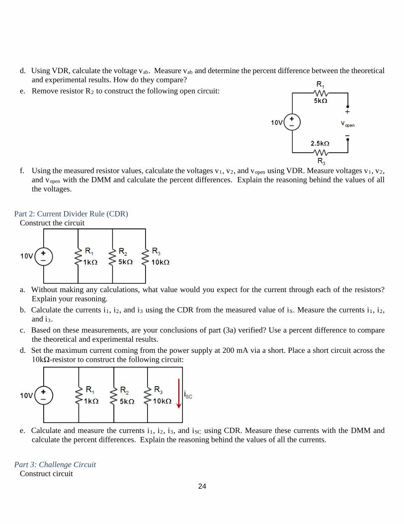
d. Using VDR, calculate the voltage vab. Measure vab and determine the percent difference between the theoretical and experimental results. How do they compare?
e. Remove resistor R2 to construct the following open circuit:
f. Using the measured resistor values, calculate the voltages v1, v2, and vopen using VDR. Measure voltages v1, v2,
and vopen with the DMM and calculate the percent differences. Explain the reasoning behind the values of all the voltages.
Part 2: Current Divider Rule (CDR) Construct the circuit
a. Without making any calculations, what value would you expect for the current through each of the resistors?
Explain your reasoning. b. Calculate the currents i1, i2, and i3 using the CDR from the measured value of iS. Measure the currents i1, i2,
and i3. c. Based on these measurements, are your conclusions of part (3a) verified? Use a percent difference to compare
the theoretical and experimental results. d. Set the maximum current coming from the power supply at 200 mA via a short. Place a short circuit across the
10kΩ-resistor to construct the following circuit:
e. Calculate and measure the currents i1, i2, i3, and iSC using CDR. Measure these currents with the DMM and
calculate the percent differences. Explain the reasoning behind the values of all the currents.
Part 3: Challenge Circuit Construct circuit

25
a. Calculate the voltages v1, v2, v3 and v4 using the VDR with measured resistor values. Measure the voltages v1,
v2, v3 and v4 and use a percent difference to compare the calculated and measured results. How do they compare?
b. Using the results of part (3a), calculate the voltage vab using KVL. c. Measure the voltage vab and use a percent difference to compare the calculated and measured results. How do
they compare? Is the voltage vab equal to v1 – v3? Equal to v2 – v4? Explain your reasoning? d. Challenge: suppose now that a short is placed across the terminal points ab. Calculate the current iab through
the short. Measure the current iab and use a percent difference to compare the theoretical and experimental results. How do they compare?

26
Mesh & Nodal Analysis EXPERIMENT 10
OBJECTIVES 1. Practice wiring several voltage sources on a bread board using one power supply. 2. Demonstrate the validity of Mesh and Nodal analysis through experimental measurements. 3. Use Loop currents to predict voltages across resistors and Node voltages to determine current through resistors.
EQUIPMENT Lab Kit and Power Supply
THEORY The mesh analysis determines the mesh or loop currents of the circuit, while the nodal analysis will provide the
potential levels of the nodes with respect to some reference. The application of each technique follows a sequence
of steps, each of which will result in a set of equations with the desired unknowns. It is then only a matter of solving
these equations for the various variables, whether they are current or voltage.
Part 1: Mesh Analysis
Construct the circuit
a. Use PSpice to simulate the loop currents. (Hint: use 0-V sources to indicate the current direction.) b. Use mesh analysis to predict the loop currents (i1, i2, i3) of the circuit. Make sure to label the loop currents and
indicate their directions. Include all your calculations and organize your work. c. Energize the circuit and measure all the loop currents. d. Compare the following two sets of data:
• Compare the PSpice and theoretical loop currents using a percent difference. How do they compare? • Compare the theoretical and experimental loop currents using a percent difference. How do they compare? Organized all your data values into a table!
e. Using your loop currents (i1, i2, i3), predict and measure the voltages across R2 and R3, and compare them with measured values using a percent difference. How do they compare?

27
Part 2: Nodal Analyses Construct the circuit
a. Use PSpice to simulate the node voltages. b. Use node analysis to predict the node voltages of the circuit. Make sure to label all the nodes. Include all your
calculations and organize your work. c. Energize the circuit and measure the node voltages. d. Compare the following two sets of data:
• Compare the PSpice and theoretical node voltages using a percent difference. How do they compare? • Compare the theoretical and experimental node voltages using a percent difference. How do they compare? Organized all your data values into a table!
e. Using your node voltages (v2, v3), predict and measure the currents through resistors R1, R2 and R3, and compare them with measured values using a percent difference. How do they compare?
Part 3: Bridge Network Construct the circuit
a. Use PSpice to simulate the voltage drop (v5) and the current through (i5) resistor-R5. b. Use Node analysis to predict the voltage v5 and Mesh analysis to predict the current i5. c. Energize the circuit and measure the voltage v5 and current i5.

28
d. Compare the predicted and measured results using a percent difference? How do they compare? e. Many times one is faced with the question of which method to use in a particular problem. This laboratory
activity does not prepare one to make such choices but only shows that the methods work and are solid. From your experience in this activity, summarize in your own words which method you prefer and why for this circuit.
Thévenin’s Theorem EXPERIMENT 11

29
OBJECTIVES 1. Become aware of an experimental procedure to determine vTh and RTh 2. Validate Thévenin’s theorem through experimental measurements using two methods. 3. Validate the maximum power transfer relation for a Thévenin circuit.
EQUIPMENT Lab kit, Decade Resistor Box, Power supply
THEORY Through the use of Thévenin’s theorem, a complex two-terminal, linear, multisource dc circuit can be replaced by one having a single source and resistor. The Thévenin equivalent circuit consists of a single dc source referred to as the Thévenin voltage and a single fixed resistor called the Thévenin resistance. The Thévenin voltage is the open-circuit voltage across the terminal points of the load. The Thévenin resistance can be calculated using two methods: Method-1: Determine the Thévenin resistance when all sources deactivated. Method-2: Determine the Thévenin resistance using the ratio of the Thévenin voltage to the short circuit current of
the load resistance – vOC/iSC.
PROCEDURE Construct the circuit
Part 1: The Theoretical Thévenin Equivalent Circuit Part 1A – Method-1: Thévenin Resistance with Deactivated Sources a. Remove the load resistor at the terminal points a-b and predict the theoretical Thévenin resistance (RTh)thy-1
with all sources deactivated. b. Deactivate all the sources in the circuit and measure the experimental Thévenin resistance (RTh)expt using a
DMM. Compare the predicted and experimental Thévenin resistances using a percent difference. How do they compare?
Part 1B – Method-2: Thévenin Resistance using vOC/iSC Short-Circuit Current iSC

30
a. Remove the load resistor at the terminal points a-b and insert a short. Predict the short circuit current (isc)thy-2 with all sources activated. Show all work!
b. Energize the circuit and measure the short circuit current (isc)expt-2. Compare the predicted and experimental short circuit current using a percent difference. How do they compare?
Open-Circuit Voltage vOC c. Remove the short between the terminals points a-b and predict the open circuit voltage vOC = (vTh)thy. d. Energize the circuit and measure the open circuit voltage (vTh)expt. Compare the predicted and experimental
short circuit current using a percent difference. How do they compare? Thévenin Resistance e. Predict the Thévenin resistance using Method-2: (RTh)thy-2 = (vTh)thy /(isc)thy-2. Compare the predicted and
measured Thévenin resistance using the measured Thévenin resistance obtained from Part (1Ab). How do they compare?
f. Compare the Thévenin resistances for both methods ((RTh)thy-1 and (RTh)thy-2) – how do they compare? Use sentence concise sentences to explain whether both methods are equivalent?
Part 2: The Experimental Thévenin Equivalent Circuit
a. Do not break down your circuit. Construct a second circuit on the breadboard – the Thévenin equivalent circuit
where the Thévenin resistance is the measured value obtained in part (1Ab) and the Thévenin voltage is the measured value obtained in part (2Bd).
b. Measure the current through the load resistor iload in both the original and the Thévenin equivalent circuits. c. Compare load resistor currents for both the original and the Thévenin equivalent circuits using a percent
difference. How do they compare? d. Use short concise sentences to explain whether Thévenin’s theorem has been verified?
Part 3: Maximum Power Transfer (Validating the condition RL = RTh) a. In the original circuit, replace the load resistance with a Decade Resistor box. Note that the Thévenin resistance
is the resistance already on your circuit board. b. Measure the voltage across the Decade box as the resistance is changed in increments of 100
and ending at 2k . A c. Set up a data table of Rload, vload, and Pload and plot Pload verse Rload.

31
d. Referring to your plot, what value of Rload resulted in maximum power transfer to the load resistance? How do the theoretical and measured values compare?
Part 4: The PSpice Thévenin Circuit
a. Use PSpice to find the Thévenin voltage vTh and resistance RTh. b. To simulate the Thévenin voltage vTh, “Capture” a circuit when the load resistance is replaced with a 5G
resistor. The voltage across the load will be the open circuit voltage vOC = vTh. Hint: place the ground at one of the nodes of the load resistance.
To simulate the Thévenin resistance RTh, use the relationship RTh = vOC/iSC. Make a second copy of the above circuit, renumber the parts in the duplicate circuit, and
c. replace the load resistance with a short circuit wire. The current through the 5V source will be the short circuit current iSC.
d. Simulate both two circuits simultaneously on the same page. Calculate RTh using RTh = vOC/iSC. e. **To Simulate the Power for the Thévenin’s circuit do the following:
• Define the resistor value as RL and call the resistor Rload. • Choose the element PARAM, define a new parameter by creating a new column and define the RL
with any resistor value like 1k • Perform a dc sweep, global parameter RL, set up the rest of the input values. Careful: do set the initial
to zero but 1
Method-1 thy expt %diff RTh
Method-2 thy expt %diff RTh
thy expt %diff
3k
-31.25V
Open Circuit5G
0
0V
a
2.2k
b15V
4.7k
20V
1k
1k
1k
-3.931V
a4.7k Rload
4.7k
5.092mA
20V20.00V
3k
1k
2.2k
0
15Vb
2.2k
20V
b
1k
1k
Short-Circuit0V
21.74mA
0
a3k4.7k
15V

32
PSpice: Time Domain Analysis EXPERIMENT 12
vTh

33
OBJECTIVES 1. Use PSpice Circuit Simulator to simulate circuits containing capacitors and inductors in the time domain. 2. Practice using a switch, and a Pulse & Sinusoidal voltage source in RL and RC circuits.
EQUIPMENT PSpice Program
THEORY The inputs to an electric circuit have generally been independent voltage and current sources. PSpice provides a set of voltage and current sources that represent time varying inputs. “Time Domain (Transient)” analysis using PSpice simulates the response of a circuit to a time varying input. Time domain analysis is most interesting for circuits that contain capacitors or inductors. For the capacitor, the part properties of interest are the capacitance and the initial voltage of the capacitor (the “Initial Condition”). For the inductor on the other hand, the part properties of interest are the inductance and the initial current of the inductor (the “Initial Condition”).
In this lab we consider three examples. The first example illustrates transient analysis of a RL circuit with s single switch; the second and third circuits analyzed are the response of an RC circuit to a Pulse voltage source and a sinusoidal voltage source.
We will again use a five-step procedure to organize circuit analysis using PSpice.
Part 1: Transient Analysis of an RL Circuit with a Switch Time varying voltages and currents can be caused by opening or closing a switch. PSpice provides parts to represent single-pole, single-throw (SPST) switches in the parts library. These parts are summarized below: Description: Open switch will close at t = TCLOSE;
Open switch will close at t = TCLOSE;
Pspice Name: Sw_tCLOSE Sw_tOPEN
Library: Eval
PSpice Problem The circuit shown is at steady state before the switch closes at time t = 0.
The current in the inductor before the switch is closed is iL(t = 0) = 40 mA. Find the current of the inductor as a function of time after the switch closes. That is, use PSpice to simulate the circuit after the switch closes.
Analytical Solution: set iL(0−) = 40 mA and ISC = 60 mA.
I I t / 40000tL SC L SCi (t) (i (0 ) ) e (60 20e ) mA− − −τ= + − ⋅ = −
U1
TCLOSE = 01 2
U2
TOPEN = 01 2

34
where τ = L/RTh = 25µs.
Step 1: Formulate a circuit analysis problem After the switch closes the circuit’s time constant is 25 µs. Plot the inductor current, iL(t), for the first 150 µs (6 time constants) after the switch closes.
Step 2: Describe the circuit using Capture Place the parts (an inductor has terminal points 1 & 2 that indicate a positive and negative polarity, respectively) and set the initial condition iL(0−) = 40 mA. That is, double click on the inductor and set the property named “IC” ≡ initial condition = 40mA.
Step 3: Simulate the circuit using PSpice. Edit the Simulation to be “Time Domain (Transient)”.The simulation starts at time zero and ends at the "Run to time". Specify the "Run to time" as 6τRL = 150 µs and run it.
Step 4: Display the results of the simulation using Probe After a successful simulation, a Probe window will automatically open. Add trace I(L1:1) (the current through inductor L1 through node 1) and the resulting plot is
Hints i. To remove grid lines from the plot, right-click on the plot and select settings. Under the X & Y Grid tabs, select
none two times. One can set this as the default by clicking “Save As Default.” ii. To change the color or thickness of a line, edit Trace Properties. iii. To copy this plot go to the “Window” tab on the tool bar and select “copy to clipboard” and paste into your
document. iv. To search for specific values, click the “Toggle Cursor” followed by the “Search Cursor”. Type in the
commands SFXV (xvalue) for x-values or SFLE (yvalue) for y-values.
Step 5: Verify that the simulation results are correct. The initial response of the inductor current is iL(0−) = 40 mA and its final state current is ISC = iL(∞) = 60 mA. Verify that the plot agrees with the mathematical prediction.
To ask a more detail questions such as what is the value of iL(t) at a time of 30.405 µs, there are several tools that are at our disposal: the Probe cursor button and Mark Data points & adjust value buttons allow one to select a particular data value on the curve. To find the current at t = 30.405 µs, one can find that the plot indicates that iL(t) = 53.592 mA when t = 30.405 µs. Substituting t = 30.405 µs into the complete natural response gives iL(t) = 54.073 mA, a difference of 0.5%. The simulation results are correct.
Part 2: The Response of an RC Circuit to a Pulse Input PSpice Problem

35
The source voltage and RC circuit are
Use PSpice to simulate the voltage source and the capacitor’s voltage vC,PS(t) and compare it to theoretical prediction
1000t
C,thy 1000(t 0.002)
4 (1 e ) 0 t 2 msv (t)
1 4.46 e 2 ms t 10 ms
−
− −
⋅ − < <= − + ⋅ < <
Step 1: Formulate a circuit analysis problem Plot three voltages simultaneously: VS (t), vR(t) and vC(t) vs t.
Step 2: Describe the circuit using Capture. Place the parts, adjust parameter values and wire the parts together. The voltage and current sources that represent time varying inputs are provided in the “SOURCE” parts library. In our circuit, the voltage source is a VPULSE part.
The plot of vin(t) shows making the transition from -1 V to 4 V instantaneously. Zero is not an acceptable value for the parameters tr or tf. Choosing very small value for tr and tf will make the transitions appear to be instantaneous when using a time scale that shows a period of the source waveform. In this example, the period of the source waveform is 10 ms so 1 ns is a reasonable choice for the values of tr and tf.
Set td, the delay before the periodic part of the waveform, to zero. Then the values of v1 and v2 are -1 and 4, respectively. The value of pw is the length of time that v2 = 4V, so pw = 2 ms in this example. The value of per is the period of the pulse function, 10 ms.
Nodes can be given more convenient names using an “off-page connector:” OFFPAGELEFT-R or OFFPAGELEFT-L. Edit the properties naming each connector with “SOURCE” and “CAP.”
Step 3: Simulate the circuit using PSpice. Specify the run time for two periods (20 ms).

36
Step 4: Display the results of the simulation, for example, using Probe. Add traces V(SOURCE), V(CAP), and V(SOURCE)−V(CAP).
Go back and change the pulse width to 5ms. How do the resulting plots look like?
Step 5: Verify that the simulation results are correct. To verify the results, label four points (two from each RC curve) and check with the predictions of the complete natural response. I’ve done two of them, now you check the other two listed in the table below.
Part 3: The Response of an RC Circuit to a Sinusoidal Input PSpice Problem Use PSpice to plot the capacitor’s voltage vC,PS(t) and power PC(t) delivered to the capacitor
where
C
C C C
v (t) 1.55sin(2 10t 76.6 ) VP (t) v (t) i (t) 3.77sin(40 t 153 ) W
= π − °
= ⋅ = π − °
Step 1: Formulate a circuit analysis problem. Simulate the circuit to determine the capacitor voltage, vC(t). Plot the vC(t) versus t. Also, plot the power delivered to the capacitor as a function of time.
Step 2: Describe the circuit using Capture. Use capacitor C/ANALOG_P such that node-1 is the positive polarity
t(ms) vC,PS(V) vC,thy(V) % 1.9912 3.4638 3.4539 0.3 2.7876 1.0551 1.0551 2.4 12.000 3.3385 12.757 1.0506

37
Step 3: Simulate the circuit using PSpice. Specify the run to time as 0.8s to run the simulation for eight full periods.
Step 4: Display the results of the simulation. In the Probe window, add the trace V(CAP). One observes that the plot is disappointing for a couple of reasons. First, it's a very rough representation of a sine function. Second, it takes a while for the capacitor voltage to settle down. In other words, the capacitor voltage includes a transient part as well as the steady state response. In this example, we only want the steady state response and so would like to eliminate the transient part of the response.
• To obtain a smoother plot, edit the Simulation Settings and set the "Maximum step size" to smaller step size: 0.001s.
• The transient part of the capacitor’s voltage can be eliminated by adjusting the initial capacitor’s voltage to
Cv (t 0) 1.55sin(20 t - 76.6 ) V 1.55sin(76.6 ) 1.506 V= = π ° = − ° = − Set the initial condition (IC) of the capacitor to be this value.
With these two adjustments, the resulting plots are
What to turn in. 1. The circuit is at steady state before the switch is thrown at t = 0.
a. Determine and plot the voltage across the capacitor vC(t) and the current i2kΩ(t) through the 2kΩ resistor for t > 0. PSpice does not let you plot current and voltage simultaneous since they have different units.

38
b. Simulate the circuit, print out the plots and explain (using short concise sentences) the behavior of the capacitor and 2kΩ resistor using your plots.
2. Turn in parts 1, 2 and 3 of the PSpice lab. Make sure that you show your work for verifying the simulation results!

39
The Response of an RC Circuit EXPERIMENT 13
OBJECTIVES 1. Validate the RC response for a partially and fully charging/discharging capacitor. 2. Check the validity of Kirchhoff’s Voltage Law for an RC circuit.
EQUIPMENT Lab kit, Oscilloscope, Function Generator, Power Supply
THEORY Consider the Thévenin RC circuit with the square wave voltage input. The time dependent voltage across the capacitor is
t / t /
C OC C OC final initial finalv (t) V (v (0 ) V )e V (V V )e− − τ − τ+ − + −= ≡ What determines whether a capacitor is partially or completely charged is the pulse width (pw) of the square wave input. Two cases will be considered: (1) pw = 5τ and (2) pw = 2. For a pulse width of 5τ or greater, the capacitor will have enough time to completely charge up and completely discharge. For a pulse width of 2τ, the capacitor will not have had enough time to completely charge up or completely discharge. It will require 5 cycles of the constant square wave input to reach its final steady state value. The repeated application of the complete response for a constant input for these 5 cycles will ultimately achieve the final steady-state value that is observed experimentally on the oscilloscope.
PROCEDURE
Part 1: Setting up the Function Generator a. Set the function generator to the square-wave mode and set the frequency to 10 kHz. b. Adjust the amplitude until a 10V (p-p) signal is obtained. Adjust the function generator’s OFFSET to 5-volts to
offset the negative pulse. Then adjust the zero reference line at the bottom of the screen to increase the accuracy for measuring voltages
c. Now adjust the sweep control until two full periods appear on the screen. Using the scope display, adjust the frequency of the function generator to ensure that the output frequency is exactly 10 kHz. (Hint: determine how many horizontal divisions should encompass a 10-kHz signal, and make the necessary adjustments.)
d. How is the pulse width pw and period T of the square wave voltage related to the frequency f for the cycle?
Part 2: RC Response for a pulse width of 5
Construct the following circuit.

40
Part 2A: Measurements for a pulse width of 5τ a. Determine the time constant τ of the circuit using the actual resistor and capacitor values that will be used in
the experiment. b. From the time constant , determine the period T = 10τ required for a capacitor to fully charge and discharge.
Using the period, determine the frequency for the voltage source. c. Adjust the function generator in order to see the charging and discharging of the capacitor (that is, at least 10 ). d. Predict the capacitor’s and resistor’s voltage (vC-thy(t) & vR-thy(t)) for the charging phase for time constants
(τ, 3τ, 5τ) and for the discharging phase for time constants (6τ, 8τ, 10τ) Hint: an excel spread sheet calculations will reduce the redundancy; however, a sample calculation is still required.
e. Measure the capacitor’s voltage vC-expt(t) for the charging and discharging phases. Make sure that the capacitor is connected to the ground and make the necessary adjustments to ensure that the total waveform is on the screen.
f. Switch the positions of the resistor and capacitor. Measure the resistor’s voltage
vR-expt(t) for the charging and discharging phases. Accurately plot vC-expt(t) and vR-expt(t) on the same graph paper.
g. Compare the predicted and measured values for the capacitor’s and resistor’s voltages during the charging and discharging phases. How do they compare?
h. Use KVL to make sure that the voltage source value equals the sum of the resistor and capacitor voltages (vS =
vR + vC) at time t = 3τ. Make this comparison graphically as well as numerically. Does KVL hold for RC circuits? Explain.
Part 2B: PSpice Simulation
Simulate the RC circuit using the determined time constant.
Part 3: RC Response for a pulse width of 2τ Part 3A: Measurements for a pulse width of 2τ a. From the time constant, determine the period T, the pulse width T/2, and the frequency f of the applied square
wave. c. Adjust the function generator in order to see the charging and discharging of the capacitor. Is the capacitor full
charging and discharging? Explain your reasoning.
0
R
1k
10V(p-p) C 0.01uFVpulse

41
d. Predict and measure the capacitor’s and resistor’s voltages (in steady-state) using the same process as in part (2A). For the charging phase use the times (τ and 2τ) and for the discharging phase (3τ and 4τ).
e. Compare the predicted and measured values for the capacitor’s and resistor’s voltage during the charging and discharging phases. How do they compare?
f. Use KVL to make sure that the voltage source value equals the sum of the resistor and capacitor voltages (vS =
vR + vC) at time t = τ. Make this comparison graphically as well as numerically. Does KVL hold for RC circuits? Explain.
Part 3B: PSpice Simulation for a pulse width of 2τ
Simulate the RC circuit using the determined time constant.
The Response of an RL Circuit EXPERIMENT 14

42
OBJECTIVES
1. Observe the effect of frequency on the impedance of a series RL circuit. 2. Plot the voltages and current of a series RL circuit versus frequency & interpret them. 3. Predict and plot the phase angle of the total impedance versus frequency for a series RL circuit and relate them
to the Phasor voltages.
EQUIPMENT Lab Kit, oscilloscope, and Function Generator
THEORY Series RL According to the voltage divider rule (VDR), in a series RL circuit, the voltage vL (vR) is directly related to the inductive reactance XL (resistive reactance R):
LL source R source
X Rv v and v vZ Z
= =
where the internal resistance of the inductor is ignored and the total impedance is
( )π 22 2 2LZ R X R 2 fL= + = +
Since the inductive reactance XL increases with increasing frequency changes (XL = 2 fL), the voltage drop across the inductor will also increase with frequency. However, the resistive reactance is independent of frequency changes. The phase angle associated with the impedance Z is also sensitive to the applied frequency
1 LXθ tanR
−=
At very low frequencies the inductive reactance will be small compared to the series resistive element (R >> XL) and the network will be primarily resistive in nature. The result is a phase angle associated with the impedance Z that approaches 0O (V and I in phase). At increasing frequencies, inductive reactance will drown out the resistive element (XL >> R) and the circuit will be primarily inductive, resulting in a phase angle approaching 90O (V leads I by 90O).
PROCEDURE Part 1: Plotting VL, VR, and I versus Frequency
Construct the following circuit.
All voltage measurements are peak-to-peak voltages.

43
a. Maintaining the voltage source at a VS = 4V (p-p), measure the voltage VL for 1kHz increments for the frequency range of 1kHz to 10 kHz. For each frequency change, reduce the amplitude of the voltage source to maintain a 4V!
b. Turn off the voltage source and interchange the positions of R and L in the circuit. Measure vR for the same range of frequencies with VS maintained at 4V. This is a very important step. Failure to relocate the resistor R can result in a grounding situation where the inductive reactance is shorted out!
c. Calculate I = vR/R for each of the frequencies and organize a data table that includes vL, vR, I and KVL. d. Plot the voltages vL and vR versus frequency on a single graph and I versus frequency separately. Label the
curves and clearly indicate each plot point. e. Answer the following questions about the plots using short concise sentences:
• As the frequency increases, describe what happens to the voltage across the inductor and resistor using short concise sentences.
• At f = 0 Hz, does vR = Vsource? Explain why or why not. • At the point where vL = vR, does XL = R? Should they be equal? Why? Is so, identify this point on the
voltage plots. • Is KVL satisfied (vL + vR = VS)? Explain why or why not. • At low frequencies the inductor approaches a low-impedance short-circuit equivalent and at high frequencies
a high-impedance open-circuit equivalent. Does the data from your table (as well as the plots) verify this? Explain your reasoning.
f. Plot current I versus frequency, labeling the curve and clearly indicate each plot point. How do the curves of I vs. f compare to vR vs. frequency? Is the sensing resistor then a good measure of the current? Explain your reasoning.
Part 2: Z versus Frequency
a. Using the data from Part 1(VS = 4V and I), calculate the experimental and theoretical total impedance (Zexpt and Zthy) for each frequency using the following equations:
IS
exptV
=Z L2 2
thy L)(R R X= + +Z
Compare them using a percent difference. Organize your data into a table. b. Plot Z, R and XL versus frequency on the same plot. Label the curve and clearly indicate each plot point. c. Answer the following questions about the voltage plots using short concise sentences:
• As the frequency increases, describe what happens to the resistive & inductive reactance and the total impedance.
• At low frequencies is vR > vL? If f = 0 Hz, would Z = R? Explain why or why not. • Predict and compare (from your plot) at which frequency does XL = R? For frequencies less than this
frequency is the circuit primarily resistive or inductive? How about for higher frequencies? Part 3: ɵ versus Frequency
a. Using the inductive reactance XL data from Part 2, calculate and plot the phase angle ( = tan1(XL/R)) as shown in the table below.

44
b. Answer the following questions about the voltage plots using short concise sentences: • At low frequency, does the phase angle suggest resistive or inductive behavior? Explain why. Draw a Phasor
voltage diagram showing this. • At high frequencies, does the phase angle suggest a resistive or inductive behavior? Explain why? Draw a
Phasor voltage diagram showing this.
f (Hz) vL(p-p) vR(p-p) i(p-p) KVL % 0 200 500 1k 2k 3k 4k 5k 6k 7k 8k 9k 10k 100k
f (Hz) R(Ω) XL(Ω) ( ) I−
−
Ω =expt
S(p p)T
p p( )
VZ ( ) Ω = +2 2
T Lthy( ) R XZ % Difference
0 200 500Hz 1 kHz 2 kHz 3 kHz 4 kHz 5 kHz 6 kHz 7 kHz 8 kHz 9 kHz

45
f (Hz) XL Tan-1(XL/R) 100 500 1k 2k 3k 5k 10k 100k

46
Series Resonant Circuit EXPERIMENT 15 OBJECTIVES
4. Validate the basic equations for the resonant frequency of a resonant circuit. 5. Plot the various voltages and current for a resonant circuit versus frequency. 6. Verify that the input impedance is a minimum at the resonant frequency.
EQUIPMENT Lab Kit, oscilloscope, and Function Generator
THEORY Inductive reactance increases as the frequency is increased, but capacitive reactance decreases with higher frequencies. Because of these opposite characteristics, for any LC combination, there must be a frequency at which the XL equals the XC because one increases while the other decreases. This case of equal and opposite reactances is called resonance, and the ac circuit is then a resonant circuit. In a series RLC circuit, the one frequency at which XL = XC is called the resonant frequency define as
πL C R1X X f
2 LC= ⇒ =
At this frequency the circuit is in resonance, and the input voltage and current are in phase. At resonance, the circuit is resistive in nature and has a minimum value of impedance and a maximum value of current. This can be seen by solving for current in a series RLC circuit:
I S S2 2
L CT
V VR +(X X )Z −
==
As for the voltages, the voltage across the resistor, VR, has exactly the same shape as the current, since it differs by the constant R. VR is a maximum at the resonance. VC and VL are equal at resonance (fR) since XL = XC, but note that they are not maximum at the resonant frequency. At frequencies below fR, VC > VL; at frequencies above fR, VL > VC.
PROCEDURE
Part 1: Low-Q Circuit Construct the following circuit.
Vs8Vac
C
0.1uF
R
200L25mH
0
47
a. Predict the resonant frequency (fR)thy, the current at resonance (Ip-p)thy and the total impedance (ZT)thy at resonance.
b. Use PSpice to plot the current Ip-p and VR, VL, VC verses frequency using a linear AC sweep from 500 Hz to 5500 Hz.
c. Maintaining 8 V (p-p) at the input to the circuit, record the voltage VL (p-p) for the frequencies appearing in Table 1. Make sure to check constantly that VS = 8 V (p-p) with each frequency change. Do not measure the voltage VR at this point in the experiment. The common ground of the supply and scope will short out the effect of the inductive element, which may result in damage to the equipment
Table 1: Low Q Measurements
Frequency VL(p-p) VC(p-p) VR(p-p) I R(p p)p p R
V −− = I
p pT
p p
V −
−
=Z
500 Hz 1000 Hz 1500 Hz 2000 Hz 2500 Hz 3000 Hz 3500 Hz 4000 Hz 4500 Hz 5000 Hz 5500 Hz
d. Turn off the supply and interchange the positions of C and L in the circuit. Measure VC(p-p) for the same range
of frequencies. Again, turn off the supply and interchange the positions of R and C in the circuit and measure VR(p-p) for the same range of frequencies. Take additional readings near the resonance frequency. Insert the measurements in Table 1.
e. Complete Table 1 by computing the current Ip-p(low Q) and the total impedance ZT. f. Plot the total impedance ZT (low Q) versus frequency. Label the curve and clearly indicate each plot point. g. Compare the predicted (ZT)thy and measured (ZT)expt at resonance using a percent difference. How do they
compare? h. Describe in a few sentences how the total impedance of a series resonant circuit varies with frequency. Which
element has the most influence on the input impedance at the low and high ends of the frequency spectrum?
i. Plot the current Ip-p(low Q) versus frequency. Label the curve and clearly indicate each plot point. j. Compare the predicted (Ip-p)thy and measured (Ip-p)expt at resonance using a percent difference. How do they
compare?

48
k. Describe in a few sentences how the current of a series resonant circuit varies with frequency. Voltages VL, VC, and VR versus Frequency l. Plot the voltages VL(p-p) (low Q) and VC(p-p) (low Q) versus frequency on the same graph. Now plot voltage
VR(p-p) (low Q) versus frequency on a different graph. Label the curve and clearly indicate each plot point? m. At what frequency are VR, VL, and VC a maximum? Record your data in a table.
• Did VL peak before fR and VC below fR as noted in the theory? • Does the maximum value of VR occur at the same frequency noted for the current I?
Part 2: Higher-Q Circuit
We will now repeat the preceding analysis for a higher-Q (more selective) series resonant circuit by replacing the 200 Ω resistor with a 30Ω resistor and note the effect on the various plots. a. Use PSpice to plot the higher-Q current Ip-p and VR, VL, VC verses frequency using a linear AC sweep from 500
Hz to 5500 Hz. b. Repeats parts (1c) – (1m) and answer the following questions:
• How has the shape of the ZT curve changed? Is the resonant frequency the same even though the resistance was changed? Is the minimum value still equal to RT = R + RL?
• Is the maximum current the same, or has it changed? Calculate the new maximum and compare to the measured graph value. How do they compare?
• At what frequency are VR, VL, and VC a maximum? Record your data in a table • Does the maximum value of VR continue to occur at the same frequency noted for the current I? • Are the frequencies at which VL and VC reached their maximums closer to the resonant frequency than they
were for the low-Q circuit? In theory, the higher the Q, the closer the maximums of VL and VC are to the resonant frequency.
VL(p-p) VC(p-p) VR(p-p) low Q high Q

49
The Complete Response of 2nd Order RLC Circuits EXPERIMENT 16
OBJECTIVES 1. Group lab report, which requires about 5 hours outside of lab time to properly prepare for. 2. Observe Underdamped and Overdamped Responses of a capacitor’s voltage to a constant source. 3. Predict and experimentally verify particular details of the complete response of an RLC circuit.
EQUIPMENT Lab Kit, Oscilloscope, Decade Resistor Box, and Function Generator
THEORY Natural responses of RLC circuits are generated by the release of energy by the inductor or capacitor (or both) as a consequence of an abrupt change in the voltage or current in the circuit. Similarly, the force response of RLC circuits is generated when the inductor or capacitor (or both) acquire energy after a sudden application of a voltage or current to the circuit. The description of the voltages and currents in this type of circuits is done in terms of 2nd ordered equations. Applying Kirchhoff’s laws, one can derive the 2nd order equation where the source is a constant source as
2
2
20
d d
dt dt2 constant
x x x+ + =α ω
where x is the storage element variable (vC, iL). The characteristic equation and roots 2 2 2 2
0 01,2s 2 s 0 s+ α + ω = → = −α ± α − ω
determine the natural response of the storage element. There are three types: • Overdamped ( 2 2
0α > ω ): 1 2
1 2overs t s tx (t) A e A e= +
• Underdamped ( 2 20α < ω ): 2 2
1 2 0t
under d d dx (t) (A cos t A sin t)e , −α= ω + ω ω = ω − α
• Critically damped ( 2 20α = ω ): 1 2
tcriticalx (t) (A t A )e−α= +
The complete response of the storage element is given by 1 2
1 2n fs t s tx(t) x (t) x (t) A e A e B+ == + +
where B is the final steady state voltage of the storage element. PROCEDURE Part 1: The Underdamped Response Theoretical Underdamped Analysis of a 4-V Pulse
Construct the circuit

50
a. Simulate the RLC circuit for a pulse width of 1ms. b. Determine the
• 2nd order equation for the voltage of the capacitor and determine the forced response B to check that your 2nd order equation is correct
• Characteristic roots and the type of natural response. • Initial conditions vC(0-), iL(0-), and dvC(0+)/dt. Hint: dvC(0+)/dt ≠ 0. • Constants A1 and A2. • Complete response of the capacitor’s voltage for the 4-V pulse width. Assume that the storage elements
are in steady state for time 0 and 0+ c. Predict and measure the (and compare using a percent difference)
• Period (Td)thy = 2π/ωd of the underdamped oscillation of the capacitor’s voltage. • maximum capacitor voltage (vmax)thy. (Use PSpice to help with the time location of the maximum
voltage.) • Final steady state of the capacitor’s voltage (B)thy for the underdamped oscillation.
d. Describe in a few sentences if the 2nd order response of capacitor has been verified. e. Repeat parts (1a-b) for a zero-volt pulse (when the square voltage pulse turns off).
Part 2: The Overdamped Response Theoretical Overdamped Analysis of a 4-V Pulse Width a. Replace the 1kΩ with a 100Ω resistor in the RLC circuit and simulate the RLC circuit for a pulse width of 1ms. b. Determine the complete Overdamped response of the capacitor’s voltage using the same procedure as in part
(1b). c. Predict and measure the
• Maximum capacitor voltage (vmax)thy for the overdamped oscillation. (Use PSpice to help with the time location of the maximum voltage).
• Final steady state of the capacitor’s voltage (B)thy for the overdamped oscillation? d. Repeat parts (2b-d) for a zero-volt pulse (when the square voltage pulse turns off).