Embed Size (px)
Citation preview
Nanoscience on the Tip
1
UNIVERSITY OF WASHINGTON | NANOSCIENCE INSTRUMENTS
LAB UNIT 1: Introduction Scanning
Force Microscopy Specific Assignment: Setup of scanning force microscopy experiment and first
contact measurements Equipment requirements: easyScan 2 standard AFM
The student will become familiar with contact mode Scanning Force Microscopy (SFM) as an imaging technique.

LAB UNIT 1 Scanning Force Microscopy
Nanoscience on the Tip 2
LAB UNIT 1: Introduction Scanning Force Microscopy Specific Assignment: Setup of scanning force microscopy experiment and
first contact measurements
Objective The student will become familiar with contact mode
Scanning Force Microscopy (SFM) as an imaging technique.
Outcome At the end of this lab, you will be familiar with the basic
principle and technique of contact mode SFM. You will be able to mount a cantilever tip, approach the tip to a surface, image the surface and conduct force displacement measurements.
Synopsis This lab unit serves as an introduction to SFM. Materials Smooth surfaces, such as graphite, mica, uncoated compact
disc (CD), microfabricated calibration test grids Techniques Contact mode SFM
1 m
150 nm
Nanolithographically Patterned
Alkanethiols on a Gold Surface
LAB UNIT 1 Scanning Force Microscopy
Nanoscience on the Tip 3
Table of Contents
1. Assignment .............................................................................................. 1-4
2. Quiz ........................................................................................................... 1-5
2.1 Background Questions ....................................................................................... 1-5
3. Experimental Assignment ....................................................................... 1-7
3.1 Goal .................................................................................................................... 1-7
3.2 Safety ................................................................................................................. 1-7
3.3 Instrumental Setup ............................................................................................. 1-7
3.4 Materials ............................................................................................................ 1-7
3.5 Experimental Procedure ..................................................................................... 1-7
4. Introduction to Scanning Force Microscopy (SFM) ....................... 1-10
4.1 Historic Perspectives ........................................................................................ 1-10
4.2 Scanning Force Microscopy (SFM) ................................................................. 1-11
4.2.1. Contact Mode ............................................................................................... 1-11
4.2.2. AC Mode Imaging ....................................................................................... 1-12
4.2.3. Applied Force: Cantilever Deflection and Hooke’s Law............................. 1-12
4.2.4. SFM Tips ..................................................................................................... 1-13
4.3 Dip-Pen Nanolithography (DPN) .................................................................... 1-16
References ................................................................................................. 1-17
LAB UNIT 1 Scanning Force Microscopy
Nanoscience on the Tip 4
1. Assignment
In this lab, you will use the Scanning Force Microscope (SFM), also known as Atomic
Force Microscope (AFM), as both an imaging tool, and a force measuring tool. As an
imaging tool, you will use the most basic SFM imaging method: contact mode imaging.
Employing force-displacement curves you will be measuring probe-sample forces and
determine “true” normal loads.
1. (pre-lab) Read background information of Scanning Probe Microscopy in
section 4
2. Take the quiz on your theoretical understanding in section 2
3. Learn on how to mount SFM tips
4. Image the samples provided
5. Conduct force displacement curves as function of the approach/retraction speed
on three different samples. Compare the adhesion forces.
LAB UNIT 1 Scanning Force Microscopy
Nanoscience on the Tip 5
2. Quiz
2.1 Background Questions
(1) How many hydrogen atoms would you have to line up to make one nanometer?
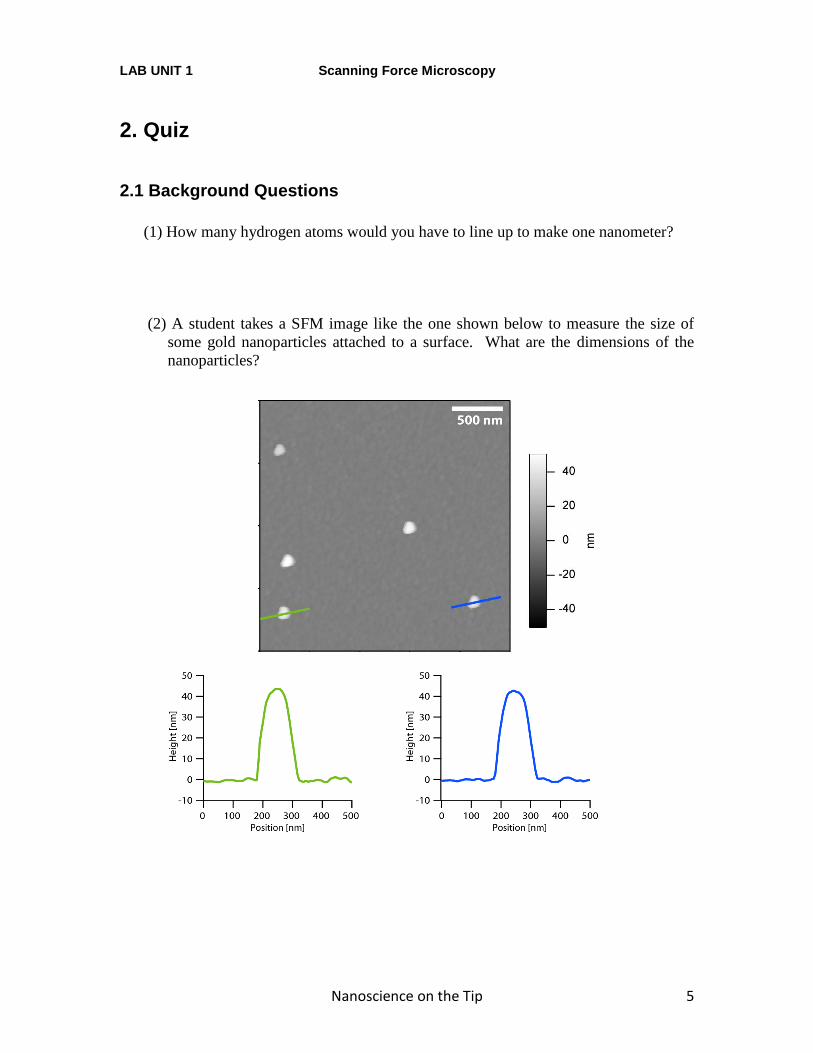
(2) A student takes a SFM image like the one shown below to measure the size of
some gold nanoparticles attached to a surface. What are the dimensions of the
nanoparticles?
LAB UNIT 1 Scanning Force Microscopy
Nanoscience on the Tip 6
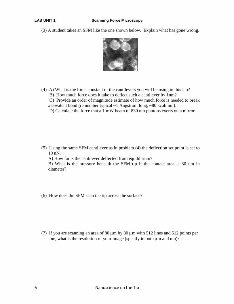
(3) A student takes an SFM like the one shown below. Explain what has gone wrong.
(4) A) What is the force constant of the cantilevers you will be using in this lab?
B) How much force does it take to deflect such a cantilever by 1nm?
C) Provide an order of magnitude estimate of how much force is needed to break
a covalent bond (remember typical ~1 Angstrom long, ~80 kcal/mol).
D) Calculate the force that a 1 mW beam of 830 nm photons exerts on a mirror.
(5) Using the same SFM cantilever as in problem (4) the deflection set point is set to
10 nN.
A) How far is the cantilever deflected from equilibrium?
B) What is the pressure beneath the SFM tip if the contact area is 30 nm in
diameter?
(6) How does the SFM scan the tip across the surface?
(7) If you are scanning an area of 80 m by 80 m with 512 lines and 512 points per
line, what is the resolution of your image (specify in both m and nm)?
LAB UNIT 1 Scanning Force Microscopy
Nanoscience on the Tip 7
3. Experimental Assignment
3.1 Goal
At the end of this lab, you should understand the concept and operation of SFM contact
mode.
Specifically perform the following:
(1) Image the materials provided on various scales by SFM.
(2) Analyze your data by processing images and performing cross-section analysis.
(3) Control the “normal load” via the force displacement curves.
3.2 Safety
- Refer to the General rules in the SFM lab
Warning: The AFM contains a Class 2M laser (650 nm wavelength). Although class
2M lasers are deemed safe for brief exposure, you should NOT look directly into the laser
beam behind the cantilever alignment chip.
3.3 Instrumental Setup
- Easy Scan 2 AFM system with contact mode AFM tip (Vista probes; CLR-25)
with 0.2 N/m spring constant, resonant frequency of 12 kHz, and the tip radius of
~10 nm
3.4 Materials
- Smooth surfaces: Graphite, Mica, microfabricated silicon calibration grids
3.5 Experimental Procedure
Read the instructions below carefully and follow them closely. If you are uncertain
about anything, please consult your TA first.
(i) Preparation – Coarse Approach
(1) System set-up: follow the start up procedure in Easy Scan 2 AFM System SOP
(Standard Operational Procedure).
a. Use a contact-mode cantilever (CLR-25)
b. Operating mode: static force (contact mode)
c. Lower the stage by clicking Advance in the Approach panel until you see
the shadow of your cantilever.

LAB UNIT 1 Scanning Force Microscopy
Nanoscience on the Tip 8
(ii) Coming to Contact
(1) Once the cantilever is approximately 1mm from its shadow,
automatic approach is used to bring the cantilever into contact.
(2) Open the Z-Controller Panel by clicking the icon right in the
Navigator bar.
(3) Set the set point to be 5 nA. Use the default values for the P-Gain, I-Gain, and D-
Gain.
(4) Click the Positioning icon (right) and under Approach options
uncheck ‘Auto start imaging’ (below left).
(5) In the Approach panel in the Positioning window (see below
right) click ‘Approach’.
(6) The software lowers the SFM tip till it comes in contact with the sample surface.
(7) Once the approach is complete a message ‘Approach done’ appears and the
imaging panel automatically appears in the active window.
(8) Look at the Probe Status Light on the Controller. If it is NOT green, it is not
operating correctly. Immediately come out of contact by clicking Withdraw in the
Approach Panel. Consult a lab assistant.
(iii) SFM Imaging
(1) Scan the selected area by going to the Imaging Panel by clicking on the Imaging
icon (right). Select the desired scan size (image width), speed (Time/Line) and
resolution in the ‘Imaging Area’ panel (below).
(2) When you have an acceptable image you wish to save, ensure
that you click the ‘photo’ icon (right) before the image is
Automatic
Approach
Click off the
Auto start
imaging
LAB UNIT 1 Scanning Force Microscopy
Nanoscience on the Tip 9
complete. This will bring up a separate box with the completed image. To save
the image go to FileSave As, create your own file on the desktop and save the
image there.
(3) Process image and perform cross-section analysis using the options under the
Tools. Keep in mind that you want to obtain the following information,
Cross-section profile of surface structures
Dimensions of your structures (report average diameter and height with
standard deviation)
Determine the surface roughness
(iv) Procedure for force spectroscopy measurement
(1) Follow the procedure described in Easy Scan 2 force distance measurement SOP.
(2) Record for the each reading;
a. Adhesion force in units of nm,
b. The temperature and the humidity
c. Any other observations that might be relevant in interpreting the results
(v) AFM shut down
(1) Follow the Easy Scan 2 AFM System SOP Shutdown Procedure

LAB UNIT 1 Scanning Force Microscopy
Nanoscience on the Tip 10
4. Introduction to Scanning Force Microscopy (SFM)
Table of Contents:
4.1 Historic Perspectives ......................................................................................................................19
4.2 Scanning Force Microscopy (SFM) ...............................................................................................20
4.2.1. Contact Mode ..........................................................................................................................20
4.2.2. AC Mode Imaging...................................................................................................................21
4.2.3. Applied Force: Cantilever Deflection and Hooke’s Law ........................................................21
4.2.4. SFM Tips ................................................................................................................................22
4.3 Dip-Pen Nanolithography (DPN) ...................................................................................................25
References ............................................................................................................................................26
4.1 Historic Perspectives
In 1982, Gerd Binnig and Heinrich Rohrer of IBM in Rüschlikon (Switzerland)
invented scanning tunneling microscopy (STM). Although STM is not the focus of this
lab, it is the ancestor of all the variations of scanning probe microscopy (SPM) that
followed: although the mechanism of image contrast may vary, the idea of building up
an image by scanning a very sharp probe across a surface has endured. As the name
suggests, STM scans a sharp tip across a surface while recording the quantum mechanical
tunneling current to generate the image. STM is capable of making extremely high
resolution (atomic resolution) images of surfaces and has been extremely useful in many
branches of science and engineering. For their invention, Binnig and Rohrer were
awarded the Nobel Prize in Physics in 19861.
Although STM is able to obtain images with better than
atomic resolution (some scientists even use it to image the
electron orbitals around atoms in molecules), one limitation
is that STM can only be used to image conductive surfaces.
In an effort to overcome this restriction, Gerd Binnig,
Christoph Gerber, and Calvin Quate at IBM and Stanford
Univeristy developed scanning force microscopy (SFM),
also known as atomic force microscopy (AFM), in 1986.
SFM is a surface imaging technique that images both
conductive and nonconductive surfaces by literally “feeling
the surface”, i.e. measuring the force between a surface and
an ultra sharp tip (typically 10 nm in radius). Fig. 4.1 shows
a SFM image of a lipid bilayer.
Figure 4.1. SFM Image of
Lipid Bilayer
(scan size: 10 nm)
LAB UNIT 1 Scanning Force Microscopy
Nanoscience on the Tip 11
4.2 Scanning Force Microscopy (SFM)
4.2.1. Contact Mode
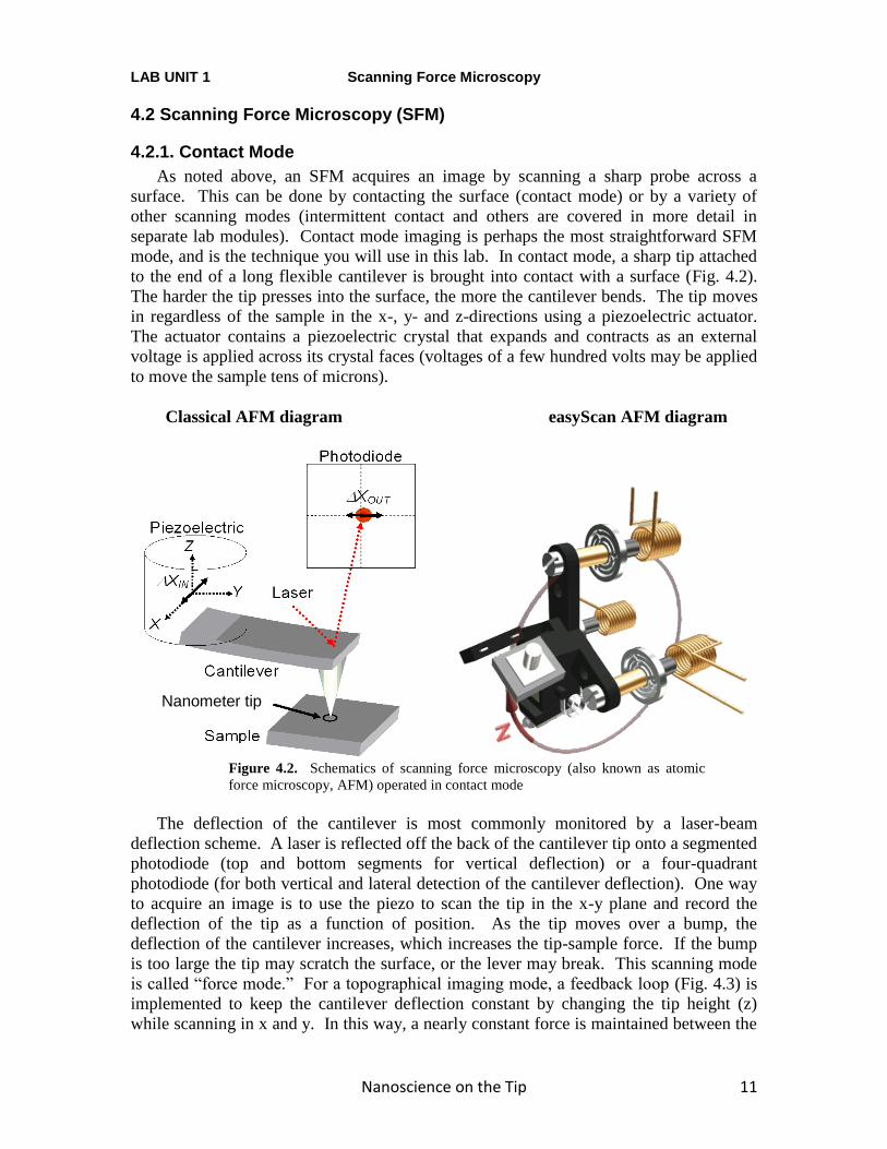
As noted above, an SFM acquires an image by scanning a sharp probe across a
surface. This can be done by contacting the surface (contact mode) or by a variety of
other scanning modes (intermittent contact and others are covered in more detail in
separate lab modules). Contact mode imaging is perhaps the most straightforward SFM
mode, and is the technique you will use in this lab. In contact mode, a sharp tip attached
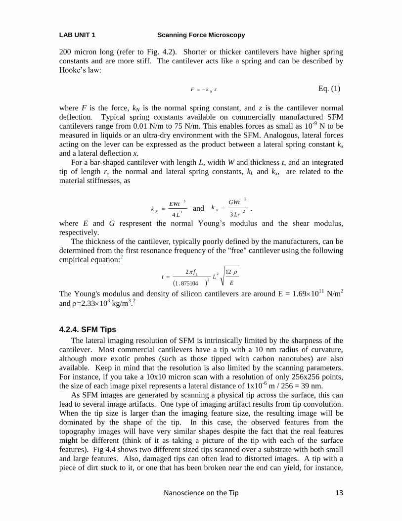
to the end of a long flexible cantilever is brought into contact with a surface (Fig. 4.2).
The harder the tip presses into the surface, the more the cantilever bends. The tip moves
in regardless of the sample in the x-, y- and z-directions using a piezoelectric actuator.
The actuator contains a piezoelectric crystal that expands and contracts as an external
voltage is applied across its crystal faces (voltages of a few hundred volts may be applied
to move the sample tens of microns).
Classical AFM diagram easyScan AFM diagram
Figure 4.2. Schematics of scanning force microscopy (also known as atomic
force microscopy, AFM) operated in contact mode
The deflection of the cantilever is most commonly monitored by a laser-beam
deflection scheme. A laser is reflected off the back of the cantilever tip onto a segmented
photodiode (top and bottom segments for vertical deflection) or a four-quadrant
photodiode (for both vertical and lateral detection of the cantilever deflection). One way
to acquire an image is to use the piezo to scan the tip in the x-y plane and record the
deflection of the tip as a function of position. As the tip moves over a bump, the
deflection of the cantilever increases, which increases the tip-sample force. If the bump
is too large the tip may scratch the surface, or the lever may break. This scanning mode
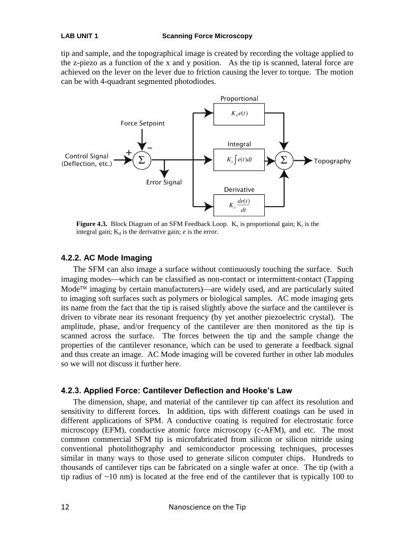
is called “force mode.” For a topographical imaging mode, a feedback loop (Fig. 4.3) is
implemented to keep the cantilever deflection constant by changing the tip height (z)
while scanning in x and y. In this way, a nearly constant force is maintained between the
Nanometer tip
LAB UNIT 1 Scanning Force Microscopy
Nanoscience on the Tip 12
tip and sample, and the topographical image is created by recording the voltage applied to
the z-piezo as a function of the x and y position. As the tip is scanned, lateral force are
achieved on the lever on the lever due to friction causing the lever to torque. The motion
can be with 4-quadrant segmented photodiodes.
Figure 4.3. Block Diagram of an SFM Feedback Loop. Kc is proportional gain; Ki is the
integral gain; Kd is the derivative gain; e is the error.
4.2.2. AC Mode Imaging
The SFM can also image a surface without continuously touching the surface. Such
imaging modeswhich can be classified as non-contact or intermittent-contact (Tapping
Mode imaging by certain manufacturers)are widely used, and are particularly suited
to imaging soft surfaces such as polymers or biological samples. AC mode imaging gets
its name from the fact that the tip is raised slightly above the surface and the cantilever is
driven to vibrate near its resonant frequency (by yet another piezoelectric crystal). The
amplitude, phase, and/or frequency of the cantilever are then monitored as the tip is
scanned across the surface. The forces between the tip and the sample change the
properties of the cantilever resonance, which can be used to generate a feedback signal
and thus create an image. AC Mode imaging will be covered further in other lab modules
so we will not discuss it further here.
4.2.3. Applied Force: Cantilever Deflection and Hooke’s Law
The dimension, shape, and material of the cantilever tip can affect its resolution and
sensitivity to different forces. In addition, tips with different coatings can be used in
different applications of SPM. A conductive coating is required for electrostatic force
microscopy (EFM), conductive atomic force microscopy (c-AFM), and etc. The most
common commercial SFM tip is microfabricated from silicon or silicon nitride using
conventional photolithography and semiconductor processing techniques, processes
similar in many ways to those used to generate silicon computer chips. Hundreds to
thousands of cantilever tips can be fabricated on a single wafer at once. The tip (with a
tip radius of ~10 nm) is located at the free end of the cantilever that is typically 100 to
LAB UNIT 1 Scanning Force Microscopy
Nanoscience on the Tip 13
200 micron long (refer to Fig. 4.2). Shorter or thicker cantilevers have higher spring
constants and are more stiff. The cantilever acts like a spring and can be described by
Hooke’s law:
zkFN
Eq. (1)
where F is the force, kN is the normal spring constant, and z is the cantilever normal
deflection. Typical spring constants available on commercially manufactured SFM
cantilevers range from 0.01 N/m to 75 N/m. This enables forces as small as 10-9
N to be
measured in liquids or an ultra-dry environment with the SFM. Analogous, lateral forces
acting on the lever can be expressed as the product between a lateral spring constant kx
and a lateral deflection x.
For a bar-shaped cantilever with length L, width W and thickness t, and an integrated
tip of length r, the normal and lateral spring constants, kL and kx, are related to the
material stiffnesses, as
3
3
4 L
EWtk
N and
2
3
3 Lr
GWtk
x .
where E and G respresent the normal Young’s modulus and the shear modulus,
respectively.
The thickness of the cantilever, typically poorly defined by the manufacturers, can be
determined from the first resonance frequency of the "free" cantilever using the following
empirical equation:2
EL
.
ft
12
8751041
2 2
2
1
The Young's modulus and density of silicon cantilevers are around E = 1.691011
N/m2
and =2.33103 kg/m
3.2
4.2.4. SFM Tips
The lateral imaging resolution of SFM is intrinsically limited by the sharpness of the
cantilever. Most commercial cantilevers have a tip with a 10 nm radius of curvature,
although more exotic probes (such as those tipped with carbon nanotubes) are also
available. Keep in mind that the resolution is also limited by the scanning parameters.
For instance, if you take a 10x10 micron scan with a resolution of only 256x256 points,
the size of each image pixel represents a lateral distance of 1x10⁻⁶
m / 256 = 39 nm.
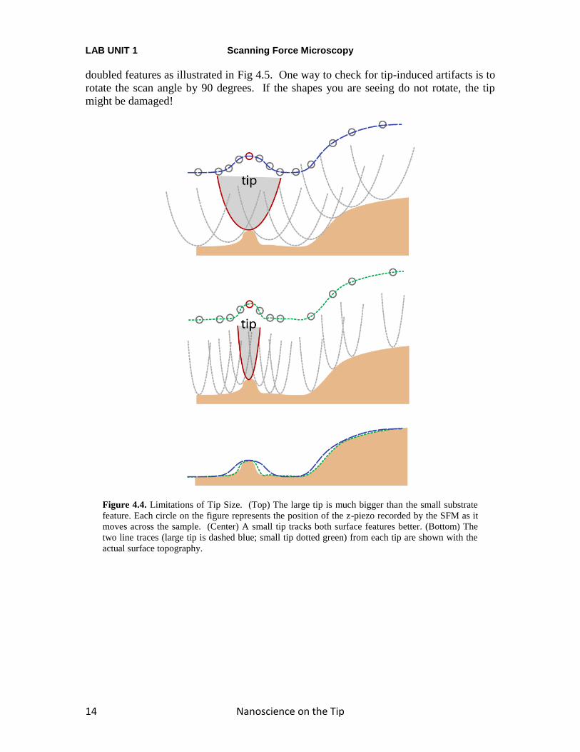
As SFM images are generated by scanning a physical tip across the surface, this can
lead to several image artifacts. One type of imaging artifact results from tip convolution.
When the tip size is larger than the imaging feature size, the resulting image will be
dominated by the shape of the tip. In this case, the observed features from the
topography images will have very similar shapes despite the fact that the real features
might be different (think of it as taking a picture of the tip with each of the surface
features). Fig 4.4 shows two different sized tips scanned over a substrate with both small
and large features. Also, damaged tips can often lead to distorted images. A tip with a
piece of dirt stuck to it, or one that has been broken near the end can yield, for instance,
LAB UNIT 1 Scanning Force Microscopy
Nanoscience on the Tip 14
doubled features as illustrated in Fig 4.5. One way to check for tip-induced artifacts is to
rotate the scan angle by 90 degrees. If the shapes you are seeing do not rotate, the tip
might be damaged!
Figure 4.4. Limitations of Tip Size. (Top) The large tip is much bigger than the small substrate
feature. Each circle on the figure represents the position of the z-piezo recorded by the SFM as it
moves across the sample. (Center) A small tip tracks both surface features better. (Bottom) The
two line traces (large tip is dashed blue; small tip dotted green) from each tip are shown with the
actual surface topography.
LAB UNIT 1 Scanning Force Microscopy
Nanoscience on the Tip 15
Figure 4.5 A minor case of doubled features caused by a damage tip. The image shows salt
crystals embedded in polymer matrix.
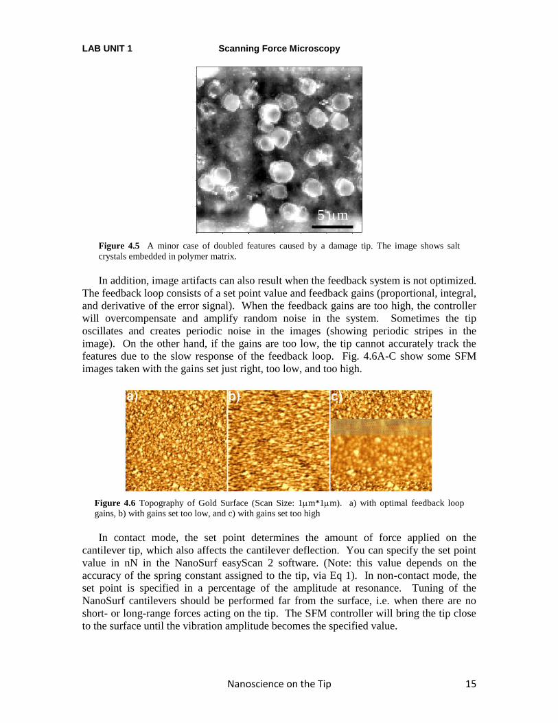
In addition, image artifacts can also result when the feedback system is not optimized.
The feedback loop consists of a set point value and feedback gains (proportional, integral,
and derivative of the error signal). When the feedback gains are too high, the controller
will overcompensate and amplify random noise in the system. Sometimes the tip
oscillates and creates periodic noise in the images (showing periodic stripes in the
image). On the other hand, if the gains are too low, the tip cannot accurately track the
features due to the slow response of the feedback loop. Fig. 4.6A-C show some SFM
images taken with the gains set just right, too low, and too high.
Figure 4.6 Topography of Gold Surface (Scan Size: 1m*1m). a) with optimal feedback loop
gains, b) with gains set too low, and c) with gains set too high
In contact mode, the set point determines the amount of force applied on the
cantilever tip, which also affects the cantilever deflection. You can specify the set point
value in nN in the NanoSurf easyScan 2 software. (Note: this value depends on the
accuracy of the spring constant assigned to the tip, via Eq 1). In non-contact mode, the
set point is specified in a percentage of the amplitude at resonance. Tuning of the
NanoSurf cantilevers should be performed far from the surface, i.e. when there are no
short- or long-range forces acting on the tip. The SFM controller will bring the tip close
to the surface until the vibration amplitude becomes the specified value.
5 m

LAB UNIT 1 Scanning Force Microscopy
Nanoscience on the Tip 16
4.3 Dip-Pen Nanolithography (DPN)
In addition to imaging with the SFM, there have been numerous methods developed
to use STM and SFM techniques as lithographic tools. STM is capable of actually
moving individual atoms, and many interesting examples of STM images can be found
online3.
Figure 4.7. Schematics of Dip-Pen Nanolithography
Dip-pen nanolithography (DPN) is a scanning probe-based lithography tool that uses
an SFM tip to “write” chemicals onto surfaces. It is a direct-write additive process. It is
analogous to a conventional fountain pen, with the SFM tip as the pen and the substrate
being the paper (Fig. 4.7). Although there are now more sophisticated systems for
delivering chemical “inks” to the tip using microfluidics, etc. (such as built-in ink
reservoir or ink wells), the basic DPN approach is still the easiest to implement. To coat
the tip with the chemical ink it is simply dipped (using tweezers and a steady hand) into
an ink solution. Alkanethiols, DNA, proteins, polymers, etc., have all been used as inks in
DPN4,5
. After the tip is inked, excess solvent is blown off the tip and it is loaded into the
SFM. When the tip contacts the substrate the chemical ink flows to the surface and is
deposited onto the surface of the substrate. For many inks, such as depositing
alkanethiols on gold, the tip can be approximated as a small source delivering a constant
flux of molecules to the surface per unit time. Thus, the area of the features increases
linearly with the dwell time (the time of contact between the tip and the surface). The
diameter of a DPN patterned feature scales approximately to the square root of the
contact time:
d t1 / 2
Eq. (2)
where d is the diameter of the patterned dots and t is the dwell time.
DPN is a direct-write technique that does not require a design mask, and it can
generate various complex structures on demand using any atomic force microscope.
However, like other scanning-probe based lithography tools, DPN is a serial process (one
feature is created at a time). Nevertheless, it is inexpensive and suitable for rapid
prototyping applications. Attempts to improve the serial natural of the DPN technique
have resulted in commercially available multiple arrays of DPN probes for mass DPN-
patterning6.

LAB UNIT 1 Scanning Force Microscopy
Nanoscience on the Tip 17
Writing patterns of a thiol (16-mercaptohexadecanoic acid, “MHA”) on a gold
surface is the most common ink-surface chemistry in DPN. Thiols chemically bond to
gold surfaces through their sulfur atom to form a gold-sulfur bond. The chemical
reaction is generally accepted to be7:
R SH A u R S A u 1
2H
2
Long-chain alkanethiols tend to form well-ordered monolayers on gold surfaces,
known as self-assembled monolayers, or SAMs. Typically, DPN-generated patterns are
characterized with LFM, allowing images of patterned SAMs to be made based on
friction contrast (i.e. the lateral defleciton of the lever if moved over the surface), e.g Fig.
4.8 (though with care it is possible to image the SAM pattern based on topography alone;
it will be very challenging to image height differences of less than a few nanometers).
Figure 4.8. Lateral Force Image of DPN-Patterned 16-Mercaptohexadecanoic Acid on Gold
Alternatively, the features can be more easily scanned in the topography mode by
using the DPN patterns as etch resists to generate topography on the gold layer after gold
etching. A common gold etching solution is a solution of thiourea and ferric nitrate8.
The amount of etched gold is proportional to the etching time. The bare, unmodified
gold (unwritten) regions will etch faster than the regions protected by the alkanethiol
SAM, as the SAM prevents the etchant molecules from reaching the gold surface.
References 1
http://nobelprize.org/nobel_prizes/physics/laureates/1986/index.html 2
Nanoscience - Friction and Rheology on the Nanometer Scale, E. Meyer, R. M. Overney et
al., World Scientific, NJ (1998). 3
http://www.almaden.ibm.com/vis/stm/gallery.html 4
D. S. Ginger, H. Zhang, and C. A. Mirkin, Angew. Chem.-Int. Edit. 43, 30 (2004). 5
K. Salaita, Y. Wang, and C. A. Mirkin, Nature Nanotechnology, 2, 145 (2007). 6
K. Salaita, Y. Wang, J. Fragala, R. A. Vega, C. Liu and C. A. Mirkin, Angew. Chem.-Int.
Edit. 118, 7378 (2006). 7
J. B. Schlenoff, M. Li, and H. Ly, J. Am. Chem. Soc. 117, 12528 (1995). 8
M. Geissler, H. Wolf, R. Stutz, E Delamarche, U.-W. Grummt, B. Michel, and A. Bietsch,
Langmuir 19, 6301 (2003).
1 m
150 nm