Embed Size (px)
Citation preview

3-1
LAB III. CONDUCTIVITY AND THE HALL EFFECT
1. OBJECTIVE
The conductivity, σ, of a silicon sample at room temperature will be determined using the van der
Pauw method. The Hall Effect voltage, VH, and Hall coefficient, RH, for the same sample will be
measured using a magnetic field. These measurements will enable the student to determine: the
type (n or p) and doping density of the sample as well as the majority carrier’s “Hall mobility.”
2. OVERVIEW
You will use the van der Pauw method to determine the conductivity of your silicon sample in
the first section of this lab. You will find the Hall voltage and coefficient in the second section.
These measurements will be used to find the semiconductor type (n or p), the doping density,
and the majority carrier mobility (Hall mobility) of the silicon sample.
Information essential to your understanding of this lab:
1. An understanding of material types (e.g,, n-type, p-type).
2. The relationship between current density and (carrier density/mobility/conductivity).
Materials necessary for this Experiment
1. Standard testing station
2. One mounted Silicon chip
3. Two magnets ~ 0.0125 Weber / m2 (1 Weber = 1 V-s) (Use them to sandwich the
sample.)
3. BACKROUND INFORMATION 3.1. CHART OF SYMBOLS
Table 1. Symbols used in this lab.
Symbol Symbol Name Units
h+ Hole Positive charge particle
e- electron Negative charge particle
q magnitude of electronic charge 1.6 x 10⁻¹⁹
C
p hole concentration (number h+ / cm
3)
n electron concentration (number e- / cm
3)
ni intrinsic carrier concentration
ND Donor concentration (number donors / cm3)
NA Acceptor concentration (number acceptors / cm3)
kb Boltzmann's constant 1.38 x 10⁻²³
joules / K
T temperature K
Eg Energy gap of semiconductor eV
J Current density A / cm2
E Electric field V / cm
conductivity ( - cm)-1
resistivity - cm
mobilities cm2 / V-sec
vd drift velocity cm / sec
B magnetic field Weber / m2
Nv valence band effective density of states cm-3
Nc conduction band effective density of states cm-3

3-2
3.2. CHART OF EQUATIONS
Table 2. Equations used in this lab.
Equation Name Formula
1
Intrinsic carrier equation )2/(2 kTE
vcigeNNn
2 Charge Neutrality p + ND = n + NA
3 Law of Mass Action pn = ni2(T)
4 Current density EEJJJ pnpn
5 Conductivity due to n nq nn
6 Conductivity due to p pq pp
7 Conductivity of a material pqnq pn
1
8 Resistivity formula for the van der Pauw
F
RRt
22ln
41,2334,12
9 Resistivity formula in terms of sheet resistance tRs
1
10 Current density xpx EJ
11 Drift velocity
xpx Ev
12 Lorentz force (y-direction) FB = qvx x Bz 13 Induced Hall Field ( yE ) zxy BqvqE
14 E-field equation for the semiconductor sample zxy BJ
qpE
1
15 Hall coefficient
qpRH
1
16 Induced E-feild zxHy BJRE
17 Hall voltage wEV yH
18 Current density twIJ xx /
19 Derivation of the carrier density in a p-type material
H
zx
V
B
t
I
qp
1
20 Derivation of Hall coefficient
zx
HH
BI
tVR
21 Derivation of the mobility
pH
p
p Rqp

3-3
3.3. CONDUCTIVITY OF A SEMICONDUCTOR
One of the most basic questions asked in semiconductor devices is “what current will flow for
a given applied voltage”, or equivalently “what is the current density for a given electric field” for
a uniform bar of semiconductor. The answer to this question is a form of Ohm's law, namely:
J = Jn + Jp = σn*E + σp*E (4)
Here, J is the current density (A/cm2) E is the applied electric field (V/cm) and σ is the conductivity
(1/(Ohm-cm)). The n and p subscripts refer to electrons and holes. This equation tells us that the
total current density J is equal to the sum of the electron and hole current densities. Those
are given by the electron conductivity * E plus the hole conductivity * E. Note that the
conductivity increases as the numbers of electrons and holes increases.
σn = q*n* μn (5)
σp = q*p* μp (6)
σ = σn + σp = q*n* μn + q*p* μp (7)
Remember q = 1.6 x 10⁻¹⁹
Coulombs and n and p are electron and hole densities (number per cm3).
The quantities μn and μp are called the “electron and hole mobilities” respectively (cm2/V-sec).
Mobilities describe the average velocity (m/s) per unit electric field that electrons or holes
experience as they propagate through the lattice of the semiconductor. In fact, we write that the
electron and hole average velocities are defined as vn = μn*E and vp = μp*E.
Note that the conductivity of a semiconductor depends upon both the carrier densities and their
mobilities. Consequently, a simple measurement of the conductivity alone can only be used to find
n and p if μn and μp are already known. (Note: The values of n and p are related by the law of mass
action (n*p = ni2) and so we only need to know either n or p to know them both.) It would be nice
if the mobilities were simple constants, but they are not. μn and μp are functions of temperature as
well as the doping concentrations (NA and ND) and therefore functions of n and p! Fortunately, we
know these functions from many prior calibration measurements done by scientists worldwide. So
a simple measurement of conductivity still can be used to give us an estimate of n and p provided
we at least know the semiconductor type (n-type or p-type). We use the Irwin curves to make the
connection between the semiconductor conductivity and its’ doping density (NA or ND). Note that
for p-type material NA ~ p and n ~ ni2/NA; for n-type material ND ~ n and p ~ ni
2/ND. Figure 1 shows
the Irwin curves. It is a plot of the silicon conductivity as a function of either NA or ND assuming
that the other is equal to zero. You should familiarize yourself with it.
There are many measurement methods to find the conductivity of a sample. One of the most
common methods is called the “four-point probe method.” We will be doing a variant of the four-
point probe method called the van der Pauw method in this lab. It is a measurement method for
arbitrarily-shaped samples. You will compare these results with measurements of the Hall
Effect. The van der Pauw method is commonly used to measure the conductivity of
semiconductors, particularly for thin epitaxial layers grown on semi-insulating substrates. You will
do this too. Using this method, you will measure the conductivity of your sample. Once you find
the resistivity of the sample, you can use the Irwin curves to estimate the values of n or p. For
example if you had a conductivity of 0.1 mho/cm (resistivity is 10 ohm-cm), NA would be
approximately 1.3 x 10¹⁵
cm-3
. Since the van der Pauw method cannot allow you to determine the
type of your semiconductor sample, you’ll have to use the Hall Effect to find that first.

3-4
Figure 1. Irwin curves for singly doped silicon at 300 K.
3.4. THE VAN DER PAUW METHOD
L. J. van der Pauw proved that the resistivity of an arbitrarily shaped sample could be estimated
from measurements of its resistance provided the sample satisfied the following conditions: 1)
contacts are at the boundary; 2) contacts are small; 3) the sample is uniformly doped and uniformly
thick; 4) there are no holes in the sample. He derived a correction factor, f, to use in that
estimation.
In the van der Pauw method, and in all 4-point probe methods, a current is forced between two
contacts (call them contacts A & B) while the voltage is measured between two different contacts
(C & D). It is often the case that UG students wonder why the voltage is NOT measured between
contacts A & B. The thought is: “Wouldn’t you get the resistance by simply dividing VAB by IAB?”
The answer is: You would get a resistance, but it would be the WRONG resistance. The resistance
that is correct is VCD/IAB. VAB/IAB gives too large a resistance because it always includes something
called the “contact resistance” too. The contact resistance is a resistance that sits exactly at the
contact between the metal probe (the contact) and the semiconductor. This resistance has a voltage
drop across it whenever there is current flowing through it (Vcontact=IAB*Rcontact.) The problem is
Resistivity
1.E-03
1.E-02
1.E-01
1.E+00
1.E+01
1.E+02
1.E+03
1.E+04
1.E+12 1.E+13 1.E+14 1.E+15 1.E+16 1.E+17 1.E+18 1.E+19 1.E+20
Dopant Concentration (cm-3
)
Res
isti
vit
y (
Oh
m-c
m)
N-type Resistivity P-type Resistivity
n-type
p-type

3-5
that this contact resistance has nothing to do with the semiconductor conductivity! Therefore, we
do not want to have Vcontact be part of our measured voltage. We want only the voltage caused by
the conductivity of our sample to be divided by IAB. Figure 2 shows a schematic diagram of this
problem. By measuring VCD on contacts with zero current flowing through them, we get no voltage
drop across Rcontact and as a result we measure only the voltage due to the resistivity.
Fig. 2. Contact resistances and the resistivity of the silicon sample. The current flowing
between contacts A&B causes a voltage drop due to the contact resistances there, but the fact that
no current flows through contacts C&D allows them to measure just the voltage due to the
resistivity.
Figure 3 shows a top view and a “3D view” of the semiconductor sample for this lab.
Fig. 3. a) a top view of the sample used in the lab; b) a 3-D view of the doped silicon material to be
tested in the lab.
Consider a doped flat semiconductor sample with an arbitrary shape, with contacts 1, 2, 3, and 4
along the periphery as shown in Fig. 4. The resistance is R12, 34 = V34/I12, where the current I12 enters
the sample through contact 1 and leaves through the contact 2 and V34 = V3 – V4 is the voltage
difference between contacts 3 and 4. The van der Pauw method then tells us that the resistivity of
the arbitrarily shaped sample is given by:
A C D B
ρ ρ ρρρ
RcontactRcontactRcontactRcontact
IAB
VCD
A B
D C
Voltmeter
a.) b.)
Contacts
A B
No Mag. Field
w
l Thickness t of
sample
3-6
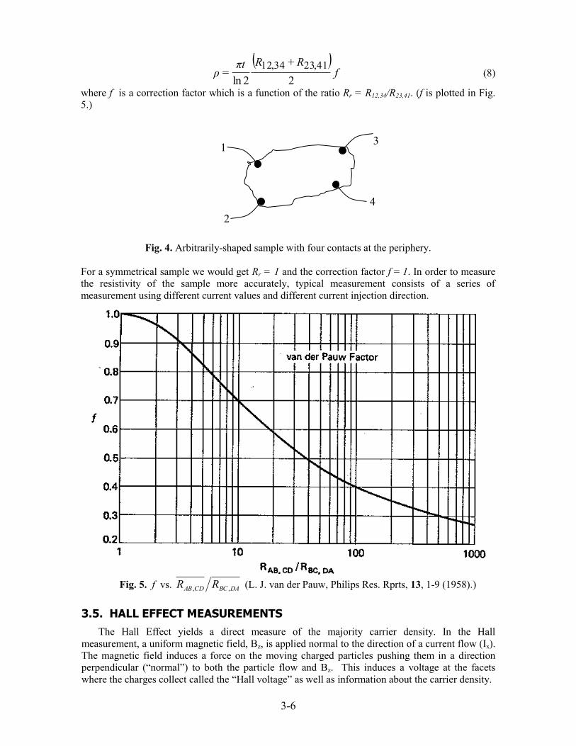
( )f
RRtπρ
2
+
2ln=
41,2334,12 (8)
where f is a correction factor which is a function of the ratio Rr = R12,34/R23,41. (f is plotted in Fig.
5.)
Fig. 4. Arbitrarily-shaped sample with four contacts at the periphery.
For a symmetrical sample we would get Rr = 1 and the correction factor f = 1. In order to measure
the resistivity of the sample more accurately, typical measurement consists of a series of
measurement using different current values and different current injection direction.
Fig. 5. f vs. DABCCDAB RR ,, (L. J. van der Pauw, Philips Res. Rprts, 13, 1-9 (1958).)
3.5. HALL EFFECT MEASUREMENTS
The Hall Effect yields a direct measure of the majority carrier density. In the Hall
measurement, a uniform magnetic field, Bz, is applied normal to the direction of a current flow (Ix).
The magnetic field induces a force on the moving charged particles pushing them in a direction
perpendicular (“normal”) to both the particle flow and Bz. This induces a voltage at the facets
where the charges collect called the “Hall voltage” as well as information about the carrier density.
1
2
3
4

3-7
In order to explain how the Hall Effect arises, we shall assume a p-type semiconductor having
the geometry shown in Fig. 6. A voltage Vx is applied to the ohmic contacts on the front and back
(B & D) which causes holes to flow in the positive x direction under the field Ex = Vx/l. The
current is given by
Jx = Ix / (w t) = σ Ex ~ σp Ex = qpμpEx = qpvx (10)
Where σ ~ σp because p >> n in p-type materials. The average hole drift velocity is:
xpx Ev (11)
Fig. 6. The fields and voltage polarities in p-type silicon for the Hall effect measurement.
In the absence of a magnetic field, the holes flow in the positive x direction. In a magnetic field,
Bz, shown in Fig. 6 to be in the +z direction, the holes experience an additional force.
FB = qvx x Bz (12)
that pushes the holes in the negative y direction. The holes thus collect at the left side of the
structure, on surface A and leave behind negatively charged acceptors at the right contact C. These
charges induce an electric field directed in the +y direction that creates an electric field induced
force opposite to the magnetic force. No current can flow in the y direction, because nothing is
connected to contacts A and C. No current flow, means that the semiconductor must have no net
force in that direction. Therefore, the two opposite forces (Bz and Ey induced) must have equal
magnitudes and
zxy BqvqE or (13)
zxy BJqp
E1
because vx = Jx/qp (14)
The Hall coefficient is defined as:
qpRH
1 (15)
So equation (14) may be re-written as:
zxHy BJRE (16)
The induced voltage between A & C is called the Hall voltage, VH:
wEV yH (17)
By using equations (15), (16) and (17) we can solve for the carrier density p:
z
y
x
A C
B
D
+ -Ey
Ix
Ex
Bz
t
w
l
Ix

3-8
H
zx
V
B
t
I
qp
1 (19)
and
zx
HH
BI
tVR (20)
Thus, p can be found from a measurement of the Hall voltage, VH, at a current Ix in a magnetic field
Bz, as shown in Fig. 6. The Hall mobility may be calculated using equation (6) and the definition of
the Hall coefficient, equation (15):
pH
p
p Rqp
(21)
Next we examine the effects obtained when an n-type sample is measured. For the applied
current Ix shown in Fig. 6, the electrons will move in the -x direction. The force due to Bz will push
the electrons in the -y direction to contact A leaving positively charged acceptors on the right side
(contact C). In this case the electric field will point in the -y direction, and the +y contact C will be
positive relative to the -y terminal A. Thus the polarity of the Hall voltage for p and n
materials is opposite. From Eq. (19), the sign of the Hall coefficient is also negative for n-type
material in this geometry.
By understanding these concepts you should be able to identify any uniformly doped
semiconductor’s carrier density and type based on the sign of the Hall voltage. You will need
this knowledge to successfully complete the Lab. If the sample was ideal, Hall voltage should be linearly increased with the applied current (Fig.
7). The Hall voltage should be linearly increased with the applied magnetic field as well.
Moreover, if the sample was ideal (i.e., there is no asymmetry in the sample), there should be no
“ohmic drop” and the measured voltage is “true” Hall voltages. However, if the sample was non-
ideal, depending on the asymmetry of the sample, the measured voltages may be shifted due to
“ohmic drop”. In this case, the measured voltage is NOT “true” Hall voltages. You must calculate
the differences between the voltages measured with and without the magnetic fields to calculate
“true” Hall voltages.
Fig. 7. Measured voltages as a function of the applied currents for ideal (no “ohmic drop”) and
non-ideal sample.
No mag. field
+ve mag. field if p-type; -ve mag. field if n-type
-ve mag. field if p-type; +ve mag. field if n-type
Ideal Condition, when sample is
symmetric and has low ohmic
drop along X direction
Practical condition, when
sample is asymmetric
Ix
Vy
Hall Voltages
SHIFT DUE TO NON-IDEAL SAMPLE

3-9
4. PREPARATION
Make sure you understand the van der Pauw and Hall theories. Before coming to the lab, solve the
following problems. Assume room temperature (300K).
1. Calculate the conductivity of an n-type Si sample with ND = 3x10¹⁵
cm-3
and n =1350
cm2/(V-sec.) using the equations found in this manual. Compare your answer with the
Irwin curve in Fig. 1. Write a two sentence statement of your findings.
2. An extrinsic p-type Si sample has a measured conductivity of = 0.1 (Ohm-cm)-1
and a
Hall voltage of 11.16 mV for Ix = 10 mA and Bz = 1,500 Gauss. The sample thickness
is 0.06 cm and the width is 1 cm. Find the doping density, NA, and the hole Hall
mobility, μp, by using both the conductivity and the Hall measurements. Hint: The
above equations are in CGS units. Convert to MKS units and note the conversion Bz =
1,000 Gauss =0.1 Weber/m2 = 0.1 Tesla. (Alternatively 10
8 Gauss = Wb/cm
2 = V-
sec/cm2).
3. Refer to the geometry of your sample shown in Fig. 9 a) and assume that it is doped n-
type with an applied magnetic field pointing out of the page. If current was flowing
from terminal A to C and you connected the negative lead of the Keithley (voltmeter)
to contact B and the positive lead to contact D what would the voltage polarity on the
voltmeter be? Assume that there is no asymmetry in the sample. Explain your answer.
5. PROCEDURE
5.1. CONDUCTIVITY MEASUREMENT USING THE VAN DER PAUW METHOD
We are going to use a doped silicon sample which has four contacts (labeled A, B, C and
D) at the corners in this Lab. The silicon sample is mounted on a board. The sample thickness (t)
is 600 μm. You will use a LabView program to measure the voltage and compute the resistivity of
the sample. The sample will yield slightly different voltages in the two orthogonal directions due
to asymmetries in the sample. The top Keithley SMU is used to measure the voltages and the
bottom Keithley SMU is used to supply the current.
You will use conductivity.vi to execute the conductivity measurement using the van der
Pauw method. If executed correctly the program will yield three columns of information with ten
entries in each column. Column 1 gives the Source Current, Column 2 gives the Source Voltage,
and Column 3 gives the Measured Voltage. You will use the Source Current and the Measured
Voltage for your calculations. Basically, you are forcing the current with the bottom Keithley and
measuring the voltage with the top Keithley.
For the first configuration in Figure 8 a), the current is passed from contact A to contact D
in discrete bursts at the incremental values set in the program by using 1 mA for the initial current,
10 mA for the final current, and 1 mA for the step current. The voltage is measured from contact B
to contact C at these different current levels giving you voltage VBC. If needed, make sure to set
the compliance voltage to a suitably high voltage. Next, you will have to configure the program to
drive the current between contact A to contact D in the opposite direction by setting the initial
current to – 1 mA, the final current to -10 mA, and the step current to – 1 mA. If needed, set the
compliance voltage to a suitably negative voltage. This will generate a voltage with the opposite
sign to VBC called VCB. Swap the leads between A to B and D and C and repeat this procedure.
For the third phase a positive current is now passed through the B and C contacts and the voltage is
measured through the A and D contacts. This should give a positive voltage VAD. Finally, the
current is reversed and the voltage again measured between A to D giving a negative voltage VDA.

3-10
Ideally the magnitude of the four voltage measurements should be exactly the same; however the
asymmetries in the geometry of the device cause some deviation in the measured voltage values.
Fig. 8. Wiring configuration for the Van der Pauw method. Bottom Keithley acts as a current
source and top source as a Voltmeter.
1. Assemble your circuit as shown in Figure 8 a). Turn on both Keithley SMUs. Open the
LabView program called Conductivity.vi located in the 3110 folder.
2. Check “yes” for the “Save Data” option. Run the program with the following settings:
Initial current: 1 mA.
Final current: 10 mA.
Step current: 1 mA.
3. This will give you a file with positive current IAD and positive voltage VBC.
4. Reverse the current to give you a negative current IDA and negative voltage VCB.
5. Convert these values to positive values for convenience.
6. Swap the leads and measure the current and voltages as above.
7. Again convert the negative values to positive values.
8. This will give you:
First: IAD = IDA = IBC = ICB
Second: VBC
Third: VCB
Fourth: VAD
Fifth: VDA
9. Save collected measurement data and compute the following in the spread sheet:
AD
BC
BCADI
VR ,
DA
CB
CBDAI
VR ,
)(2
1,,, CBDABCADBCAD RRR
A B
D C
a)
B C
KEITHLEY
(TOP)
KEITHLEY
(BOTTOM)
KEITHLEY
(TOP)
KEITHLEY
(BOTTOM)
A D
b)

3-11
BC
ADADBC
I
VR ,
CB
DADACB
I
VR ,
)(2
1,,, DACBADBCADBC RRR
)(2
1,,, ADBCBCADDABC RRR
10. Now change the leads so that they are connected as shown in Figure 8 b).
11. Repeat the above procedure.
12. This will give you:
First: IAB = IBA = IDC = ICD
Second: VDC
Third: VCD
Fourth: VAB
Fifth: VBA
13. Compute the following using your spread sheet:
AB
DC
DCABI
VR ,
BA
CD
CDBAI
VR ,
)(2
1,,, CDBADCABDCAB RRR
DC
ABABDC
I
VR ,
CD
BABACD
I
VR ,
)(2
1,,, BACDABDCABDC RRR
)(2
1,,, ABDCDCABCDAB RRR
14. Now you can find the bulk conductivity of your Si sample using the equation below and
the results from your two previous sets of calculations. Put it in your spread sheet.
FRRt CDABDABC
22ln
1 ,,
Examine Figure 5 to find the value of F, van der Pauw correction factor. Since the
semiconductor is approximately symmetric you should expect the two average resistance
measurements from your Si sample to be approximately equal to one another yielding “1”
for the ratio of DABCCDAB RR ,, .
3-12
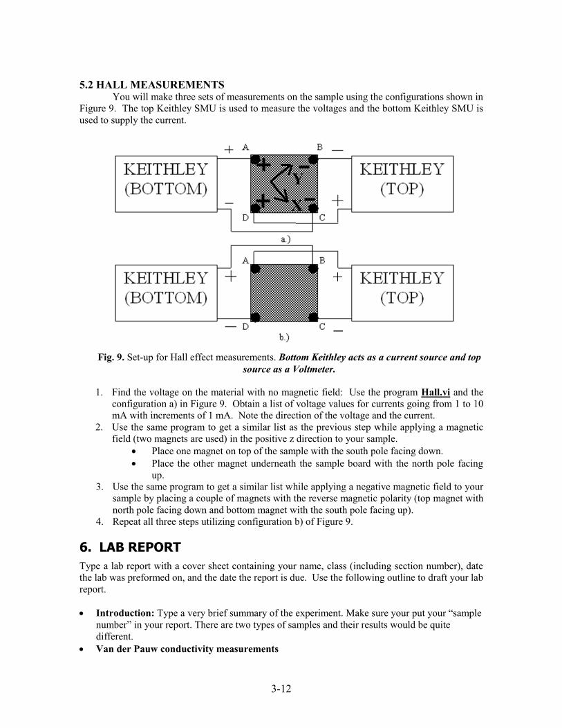
5.2 HALL MEASUREMENTS You will make three sets of measurements on the sample using the configurations shown in
Figure 9. The top Keithley SMU is used to measure the voltages and the bottom Keithley SMU is
used to supply the current.
Fig. 9. Set-up for Hall effect measurements. Bottom Keithley acts as a current source and top
source as a Voltmeter.
1. Find the voltage on the material with no magnetic field: Use the program Hall.vi and the
configuration a) in Figure 9. Obtain a list of voltage values for currents going from 1 to 10
mA with increments of 1 mA. Note the direction of the voltage and the current.
2. Use the same program to get a similar list as the previous step while applying a magnetic
field (two magnets are used) in the positive z direction to your sample.
Place one magnet on top of the sample with the south pole facing down.
Place the other magnet underneath the sample board with the north pole facing
up.
3. Use the same program to get a similar list while applying a negative magnetic field to your
sample by placing a couple of magnets with the reverse magnetic polarity (top magnet with
north pole facing down and bottom magnet with the south pole facing up).
4. Repeat all three steps utilizing configuration b) of Figure 9.
6. LAB REPORT
Type a lab report with a cover sheet containing your name, class (including section number), date
the lab was preformed on, and the date the report is due. Use the following outline to draft your lab
report.
Introduction: Type a very brief summary of the experiment. Make sure your put your “sample
number” in your report. There are two types of samples and their results would be quite
different.
Van der Pauw conductivity measurements
X
Y

3-13
o Generate V vs. I plots from the conductivity data. Calculate average value of
resistivity of the sample. You should be able to observe that all the plots almost
coincide with each other.
o Is there any indication of Joule heating in the sample? Explain what this will do to the
resistance.
o What is the room temperature conductivity of your sample? Show your calculation.
Hall measurements o Generate Vy vs. Ix plots that show your measured voltage when the magnetic field was
in the positive z direction, negative z direction and your baseline on the same graph for
both configurations in Figure 9. Remember that the measured voltages are not true
Hall voltage (VH). In order to calculate the true Hall voltage (VH), you have to find the
difference between voltages measured with and without the magnetic field. Ideally,
Hall voltages calculated with the positive magnetic field and with the negative
magnetic field should be equal in magnitude but polarity is reversed. If the calculated
voltages were not equal in magnitude, briefly explain why it is so.
o Calculate the doping density. Show your calculations. Briefly explain your
calculations.
o Calculate the majority carrier mobility. Show your calculations. Briefly explain your
calculations.
Summary o Tabulate the important results of the lab including the conductivity of the sample,
carrier mobility of the sample, type of the sample and doping concentration.