Embed Size (px)
Citation preview

DKT 122 - DIGITAL SYSTEMS I LAB 2 : INTRODUCTION TO LOGIC GATE AND ITS BEHAVIOUR
Semester 2 Session 2012/13
School of Computer and Communication Engineering 1 Universiti Malaysia Perlis
LAB 2: INTRODUCTION TO LOGIC GATE AND ITS BEHAVIOUR
OBJECTIVE 1. To verify the operation of OR, AND, INVERTER gates 2. To implement the operation of NAND and NOR gate 3. To construct a simple combinational logic circuits using CAD tool. 4. To analyze the waveforms simulated and develop truth tables from these analysis
EQUIPMENTS/COMPONENTS
Computer Unit Altera’s Quartus II Software
INTRODUCTION
This lab experiment also will introduce the ways and how to perform basic tasks using one particular software, the Altera Quartus II.
Digital circuits are often referred as switching circuits because their control devices are switches between two ON and OFF function. Logics gates have one or more inputs with one output. They respond to various input combinations. The Truth table show this relationship between circuits input combinations and its output. To determine the total number to be listed in the truth table, the equation must be presented ;
Number of combinations = 2n , where n is number or input.
The truth table for a particular circuit explains how the circuit behaves under the normal condition. In this session, five logic gates had covered such as NOT, AND, OR, NAND and NOR gate.

DKT 122 - DIGITAL SYSTEMS I LAB 2 : INTRODUCTION TO LOGIC GATE AND ITS BEHAVIOUR
Semester 2 Session 2012/13
School of Computer and Communication Engineering 2 Universiti Malaysia Perlis
PROCEDURE
Simulation Software – Altera Quartus Software A. Initialization 1. A schematic circuit design built in Quartus II requires a project name. Each time you begin with a
new design, you will need to initiate and define a new project. (All steps had been done in previous lab)
2. For this lab session, put the name of this project : AND_gate . B. Designing Circuit 1. Do the following procedure to create the schematics circuit. 2. For tutorial, construct an AND gate with two input (A and B) and an output X. 3. To begin select File | New. A pop-up window will appear inquiring the type of file that wants to
create. Select Block Diagram/Schematic File and click OK.
Figure 1(i)

DKT 122 - DIGITAL SYSTEMS I LAB 2 : INTRODUCTION TO LOGIC GATE AND ITS BEHAVIOUR
Semester 2 Session 2012/13
School of Computer and Communication Engineering 3 Universiti Malaysia Perlis
Figure 1(ii)
4. To add component in schematic spreadsheet is called editing. To edit circuit design, select Edit |
Insert Symbol. Expand the Library to show the list of subfolder. At this time, we select Logic under Primitives section because we want to design the AND gate.
Figure 1(iii)
DKT 122 - DIGITAL SYSTEMS I LAB 2 : INTRODUCTION TO LOGIC GATE AND ITS BEHAVIOUR
Semester 2 Session 2012/13
School of Computer and Communication Engineering 4 Universiti Malaysia Perlis
Figure 1(iv)
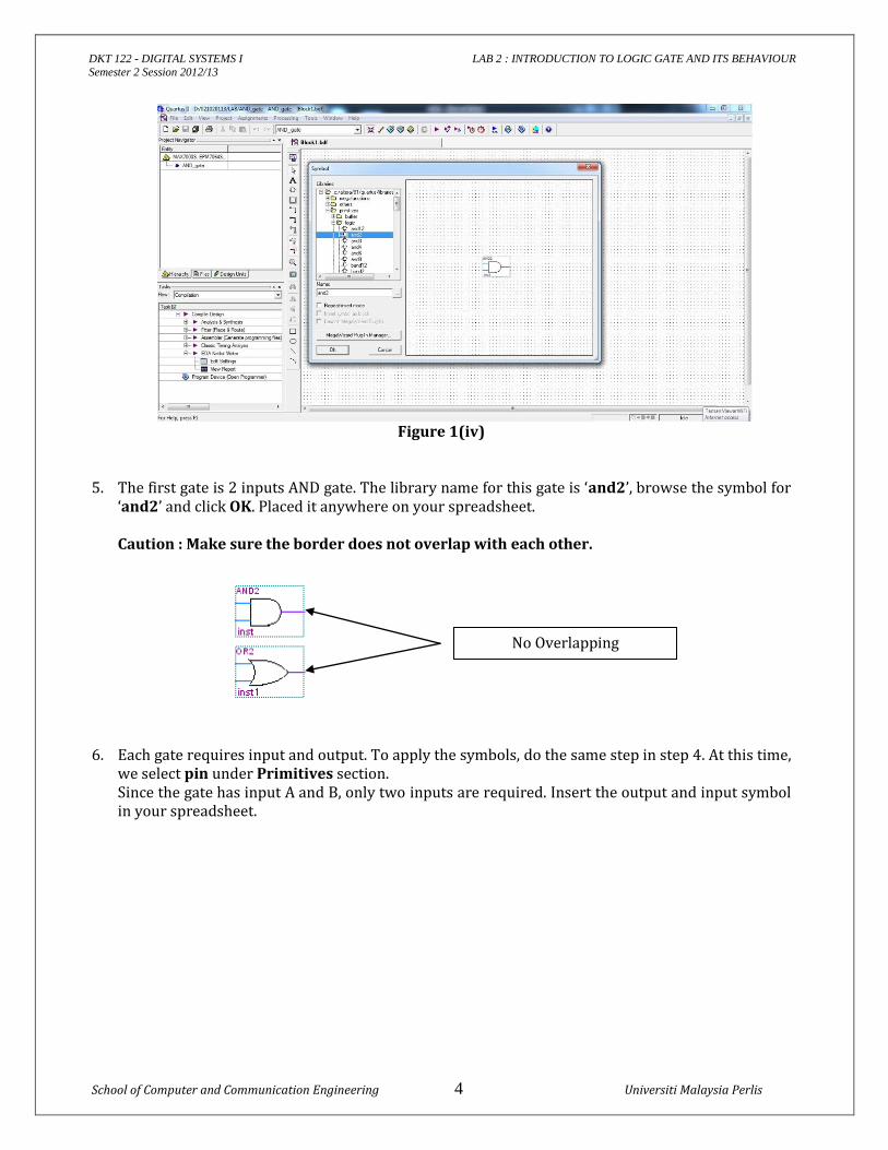
5. The first gate is 2 inputs AND gate. The library name for this gate is ‘and2’, browse the symbol for
‘and2’ and click OK. Placed it anywhere on your spreadsheet.
Caution : Make sure the border does not overlap with each other.
6. Each gate requires input and output. To apply the symbols, do the same step in step 4. At this time, we select pin under Primitives section. Since the gate has input A and B, only two inputs are required. Insert the output and input symbol in your spreadsheet.
No Overlapping

DKT 122 - DIGITAL SYSTEMS I LAB 2 : INTRODUCTION TO LOGIC GATE AND ITS BEHAVIOUR
Semester 2 Session 2012/13
School of Computer and Communication Engineering 5 Universiti Malaysia Perlis
Figure 1(v)
Basically, all gates must have input and output symbol. The input nodes are on the left side of symbol and the output nodes are on the right side.
C. Connecting Symbol Nodes with Wires
1. Go to the left side of your AND gate symbol. There are two (2) input nodes. Point your mouse on the top node. When the pointer changes to a cross, click and drag outward. A line (wire) will appear coming from this node. Connect this wire to your input “A” node. Wire the lower node to input “B”. Finally, on the right side of the AND symbol, wire the single node to the output “AND”. Complete the AND gate connection as illustrated below :
Figure 1(vi)

DKT 122 - DIGITAL SYSTEMS I LAB 2 : INTRODUCTION TO LOGIC GATE AND ITS BEHAVIOUR
Semester 2 Session 2012/13
School of Computer and Communication Engineering 6 Universiti Malaysia Perlis
2. Once done, save this spreadsheet by selecting File | Save As. A pop-up window will appear to save your spreadsheet. The name “AND_gate” will automatically appear as the name of your block diagram filename (*.bdf format). Make sure that the “Add file to current project” is ticked.
Figure 1(vii)
* Note* You can save your file anytime throughout this tutorial exercise. The earlier you save your project, the safer it is to keep your diagram updated and prevent you from starting all over if any computer malfunction such as hanging or not responding happens that may force you to reboot and restart the Quartus II software.
After building the circuit, you will need processing modules so that : (a) The overall design has no violation or component and management errors
(b) Logic design is minimized and other important files are generated
(c) Device routing placement is successful
(d) Programming files to the device are generated
(e) Timing debugs are validated
These processing modules can either come all in one or can be achieved separately. These tasks are known as a compilation process. Compilation process will cover Analysis & Synthesis, Fitter, Assembler and Classic Timing Analyzer. Remember, compilation does not check your operational design, it only checks overall design management.

DKT 122 - DIGITAL SYSTEMS I LAB 2 : INTRODUCTION TO LOGIC GATE AND ITS BEHAVIOUR
Semester 2 Session 2012/13
School of Computer and Communication Engineering 7 Universiti Malaysia Perlis
D. Performing a Compilation Process 1. To compile your design, select Processing | Start Compilation [Ctrl+L]. Quartus II will
automatically begin the compilation process and check for overall errors, debug the system for timing and arrange your project to be fitted into the selected device.
Figure 2(i)
2. A pop-up window will appear to report whether a successful or not successful has been achieved. Click OK. – For not successful compilation, double-click on the errors to locate the position of the failure.
Figure 2(ii)

DKT 122 - DIGITAL SYSTEMS I LAB 2 : INTRODUCTION TO LOGIC GATE AND ITS BEHAVIOUR
Semester 2 Session 2012/13
School of Computer and Communication Engineering 8 Universiti Malaysia Perlis
E. Performing a Simulation Process
1. To simulate your design, you must create the waveform file first. To do this, select File | New. The same New pop-up window will appear.
Figure 3(i)
2. This time go to “Other Files” tab, and select Vector Waveform File. Click OK. A blank waveform1.vwf editor file will be spread out in Quartus II.
Figure 3(ii)

DKT 122 - DIGITAL SYSTEMS I LAB 2 : INTRODUCTION TO LOGIC GATE AND ITS BEHAVIOUR
Semester 2 Session 2012/13
School of Computer and Communication Engineering 9 Universiti Malaysia Perlis
3. Some pre-settings are needed for better viewing. First is to set the end time of the waveform to only 400.0 ns. Select Edit | End Time… for the End Time pop-up window. Type 400.0 at the Time field and select ns. Click OK.
Figure 3(iii)
4. Second is to set the grid interval for each transition. To set this, select Edit | Grid Size… for the Grid Size pop-up window. In the Period field, type 50.0 and select ns. Click OK.
Figure 3(iv)

DKT 122 - DIGITAL SYSTEMS I LAB 2 : INTRODUCTION TO LOGIC GATE AND ITS BEHAVIOUR
Semester 2 Session 2012/13
School of Computer and Communication Engineering 10 Universiti Malaysia
Perlis
5. Save the file first before proceeding to the next step. For better view, select View | Fit in Window to display the entire range from 0.0ns to 1.0us with a 50.0ns grid interval.
Figure 3(v)
6. To insert the input and output nodes of your design, select Edit | Insert | Insert Node or Bus… . A pop-up window appears. Click on Node Finder.
Figure 3(vi)

DKT 122 - DIGITAL SYSTEMS I LAB 2 : INTRODUCTION TO LOGIC GATE AND ITS BEHAVIOUR
Semester 2 Session 2012/13
School of Computer and Communication Engineering 11 Universiti Malaysia
Perlis
Figure 3(vii)
7. The Node Finder pop-up window appears. At the Filter field, select “Pins: all” found from the drop down menu list. Click on the List tab. The list of all available pins will be displayed in the Nodes Found section.
8. To select which pins to be put onto the waveform, you must transfer your selection from the Nodes Found field into the Selected Nodes field. In this case, we want all input and output pins to be chosen. Transfer all pins from the Found Nodes field to Selected Nodes field.
Figure 3(viii)

DKT 122 - DIGITAL SYSTEMS I LAB 2 : INTRODUCTION TO LOGIC GATE AND ITS BEHAVIOUR
Semester 2 Session 2012/13
School of Computer and Communication Engineering 12 Universiti Malaysia
Perlis
9. Click OK at the Node Finder window. Click OK again at the Insert Node or Bus window.
Figure 3(viiii)
10. The selected input and output pins will appear at the waveform editor file. By default, input nodes will have a value of logic “0” all along the timeframe, whereas the output pins will have an unknown logic value “X”. You can select your input and output pins and rearrange them in order of your preference. Figure below shows the best possible position.
Figure 3(x)
* Note*
Notice how the symbol of the ‘A’ and ‘B’ input pins look like compared with an output pin symbol.

DKT 122 - DIGITAL SYSTEMS I LAB 2 : INTRODUCTION TO LOGIC GATE AND ITS BEHAVIOUR
Semester 2 Session 2012/13
School of Computer and Communication Engineering 13 Universiti Malaysia
Perlis
F. Setting the values on the inputs
1. As you understand, to examine the behaviour of an output, we must set the inputs to a certain value. Apart from logic ‘0’ applied to “A” and “B” input along the timeframe, these input pins must also show other values so that outputs can be fully generated when simulation occur.
n inputs will have 2n states, therefore,
2 inputs will have 22 = 4 states
2. To assign logic “1” for input “A”, click and drag at time 100ns to 200ns. The selected area will
highlight. Select Edit | Value | Forcing High (1) and the selected area will have a value of logic “1”.
Figure 4(i)
*Note*
To easily highlight the waveforms, adjust the snap to grid format so that when you click and drag an area, the selected area will snap to grid. Use the View | Snap to Grid function.
3. Apply the same method for input “B” at time interval :
a. 50ns ~ 100ns
b. 150ns ~ 200ns

DKT 122 - DIGITAL SYSTEMS I LAB 2 : INTRODUCTION TO LOGIC GATE AND ITS BEHAVIOUR
Semester 2 Session 2012/13
School of Computer and Communication Engineering 14 Universiti Malaysia
Perlis
Figure 4(ii)
4. Save your file settings when all input test patterns is made. To perform the simulation, select Processing | Simulator Tool. A Simulator Tool window appears.
Figure 4(iii)

DKT 122 - DIGITAL SYSTEMS I LAB 2 : INTRODUCTION TO LOGIC GATE AND ITS BEHAVIOUR
Semester 2 Session 2012/13
School of Computer and Communication Engineering 15 Universiti Malaysia
Perlis
5. In the Simulation mode field, select Functional from the drop down menu and click on Generate Functional Simulation Netlist button.
Figure 4(iv)
6. Click OK when a pop-up window reports a successful generation.
Figure 4(v)
DKT 122 - DIGITAL SYSTEMS I LAB 2 : INTRODUCTION TO LOGIC GATE AND ITS BEHAVIOUR
Semester 2 Session 2012/13
School of Computer and Communication Engineering 16 Universiti Malaysia
Perlis
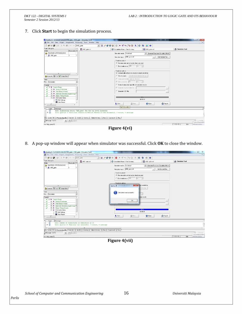
7. Click Start to begin the simulation process.
Figure 4(vi)
8. A pop-up window will appear when simulator was successful. Click OK to close the window.
Figure 4(vii)
DKT 122 - DIGITAL SYSTEMS I LAB 2 : INTRODUCTION TO LOGIC GATE AND ITS BEHAVIOUR
Semester 2 Session 2012/13
School of Computer and Communication Engineering 17 Universiti Malaysia
Perlis
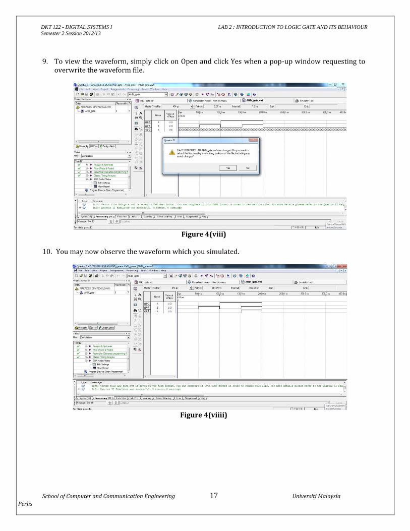
9. To view the waveform, simply click on Open and click Yes when a pop-up window requesting to
overwrite the waveform file.
Figure 4(viii)
10. You may now observe the waveform which you simulated.
Figure 4(viiii)

DKT 122 - DIGITAL SYSTEMS I LAB 2 : INTRODUCTION TO LOGIC GATE AND ITS BEHAVIOUR
Semester 2 Session 2012/13
School of Computer and Communication Engineering 18 Universiti Malaysia
Perlis
11. From the waveform generate, we can proof the result by using truth table ;
Input Output
A B X
0 0 0
0 1 0
1 0 0
1 1 1
G. Creating Symbols
Circuit designs can be very large at times. When adding a circuit onto another circuit project, the designs may become very confusing. To reduce the complications, add-on circuits can be reduced in size by just creating their symbols and adding onto another circuit design.
1. To create a default symbol for your schematic design, first you must make sure that the
AND_gate.bdf window is the active window. Select File | Create/Update | Create Symbol Files for Current File.
Figure 5(i)

DKT 122 - DIGITAL SYSTEMS I LAB 2 : INTRODUCTION TO LOGIC GATE AND ITS BEHAVIOUR
Semester 2 Session 2012/13
School of Computer and Communication Engineering 19 Universiti Malaysia
Perlis
2. The pop-up window will appear. Click on the Save button to save your design into a symbol file name AND_gate.bsf. Click OK to continue.
Figure 5(ii)
3. Open a New and select Block Diagram/Schematic File.
Figure 5(iii)
DKT 122 - DIGITAL SYSTEMS I LAB 2 : INTRODUCTION TO LOGIC GATE AND ITS BEHAVIOUR
Semester 2 Session 2012/13
School of Computer and Communication Engineering 20 Universiti Malaysia
Perlis
Figure 5(iv)
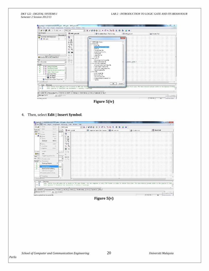
4. Then, select Edit | Insert Symbol.
Figure 5(v)

DKT 122 - DIGITAL SYSTEMS I LAB 2 : INTRODUCTION TO LOGIC GATE AND ITS BEHAVIOUR
Semester 2 Session 2012/13
School of Computer and Communication Engineering 21 Universiti Malaysia
Perlis
5. You will now see a new library called Project. Expand this library and click on AND_gate. The
preview symbol will display on the right side.
Figure 5(vi)
6. Click OK and paste anywhere on your blank spreadsheet. The circuit AND_gate now have its own
symbol for use on other schematic project. Double click the symbol and you will see the contents of this symbol.
Figure 5(vii)

DKT 122 - DIGITAL SYSTEMS I LAB 2 : INTRODUCTION TO LOGIC GATE AND ITS BEHAVIOUR
Semester 2 Session 2012/13
School of Computer and Communication Engineering 22 Universiti Malaysia
Perlis
Excercises 1. Create the basic gate diagrams for the following gates with two inputs, A and B and one output
X ; a) NOT gate b) OR gate Verify the gate operation with simulation waveforms and create the symbol for the gates above.
2. Answer the following components ; a) Verify the logic gate diagram below with simulation waveforms and complete the table
below
Input Output
A B Y Z
0 0
0 1
1 0
1 1
b) Create a symbol for the design above.
3. Evaluate the result for the Boolean expression below ;
Y = (AB)+C By using simulation waveform, show the result of Y, when the inputs are A = 1, B = 0 and C = 1
4. Briefly explain the operation of NOR and NAND

DKT 122 - DIGITAL SYSTEMS I LAB 2 : INTRODUCTION TO LOGIC GATE AND ITS BEHAVIOUR
Semester 2 Session 2012/13
School of Computer and Communication Engineering 23 Universiti Malaysia
Perlis
REPORT GUIDELINES : 1. Report must have a front page includes with ;
- Name - Matrics No - Course - Lab session
2. Answer all the exercise and submit with the given tasks.
3. Write a discussion and conclusion.