Embed Size (px)
Citation preview

L811-EU Hardware User Manual
Version: 1.0.0
Update date: 2017.06.16

Reproduction forbidden without Fibocom Wireless Inc. written authorization - All Rights Reserved.
L811-EU Hardware User Manual Page 2 of 48
Applicability Table
No. Product model Description
1 L811-EU-00 NA

Reproduction forbidden without Fibocom Wireless Inc. written authorization - All Rights Reserved.
L811-EU Hardware User Manual Page 3 of 48
Copyright
Copyright © 2017 Fibocom Wireless Inc. All rights reserved.
Without the prior written permission of the copyright holder, any company or individual is prohibited to
excerpt, copy any part of or the entire document, or distribute the document in any form.
Notice
The document is subject to update from time to time owing to the product version upgrade or other
reasons. Unless otherwise specified, the document only serves as the user guide. All the statements,
information and suggestions contained in the document do not constitute any explicit or implicit
guarantee.
Trademark
The trademark is registered and owned by Fibocom Wireless Inc.
Version Record
Version Update Date Description
V1.0.0 2017-06-16 Initial release.

Reproduction forbidden without Fibocom Wireless Inc. written authorization - All Rights Reserved.
L811-EU Hardware User Manual Page 4 of 48
Contents 1 Foreword ........................................................................................................................... 7
1.1 Introduction .......................................................................................................................... 7
1.2 Reference Standard ............................................................................................................. 7
1.3 Related Documents .............................................................................................................. 7
2 Overview ............................................................................................................................ 8
2.1 Introduction .......................................................................................................................... 8
2.2 Specification ......................................................................................................................... 8
2.3 Application Framework ......................................................................................................... 9
2.4 Hardware Framework ......................................................................................................... 10
3 Application Interface ...................................................................................................... 11
3.1 LGA Interface ..................................................................................................................... 11
3.1.1 Pin Distribution .................................................................................................................... 12
3.1.2 Pin Definition ....................................................................................................................... 13
3.2 Power Supply ..................................................................................................................... 19
3.2.1 Power Supply ...................................................................................................................... 19
3.2.2 RTC Power Supply ............................................................................................................. 21
3.2.3 1.8V Power Supply ............................................................................................................. 22
3.2.4 Power Consumption ........................................................................................................... 22
3.3 Control Signal .................................................................................................................... 23
3.3.1 Module Start-Up.................................................................................................................. 24
3.3.1.1 Start-up Circuit ......................................................................................................... 24
3.3.1.2 Start-up Timing Sequence ....................................................................................... 24
3.3.2 Module Shutdown ............................................................................................................... 25
3.3.2.1 Software Shutdown .................................................................................................. 25
3.3.2.2 Hardware Shutdown ................................................................................................. 26
3.3.3 Module Reset ...................................................................................................................... 26
3.4 USB Interface ..................................................................................................................... 27
3.4.1 USB Interface Definition ..................................................................................................... 27
3.4.2 USB Interface Application ................................................................................................... 28
3.5 USIM Interface ................................................................................................................... 29
3.5.1 USIM Pins ........................................................................................................................... 29
3.5.2 USIM Interface Circuit ........................................................................................................ 29
3.5.2.1 N.C. SIM Card Slot ................................................................................................... 29

Reproduction forbidden without Fibocom Wireless Inc. written authorization - All Rights Reserved.
L811-EU Hardware User Manual Page 5 of 48
3.5.2.2 N.O. SIM card slot .................................................................................................... 30
3.5.3 USIM Hot-Plugging ............................................................................................................. 30
3.5.4 USIM Design ....................................................................................................................... 31
3.6 UART Interface .................................................................................................................. 31
3.6.1 UART Interface Definition ................................................................................................... 31
3.6.2 UART Interface Application ................................................................................................ 32
3.7 Status Indicator .................................................................................................................. 32
3.7.1 CORE DUMP ...................................................................................................................... 33
3.7.2 LPG Signal .......................................................................................................................... 33
3.7.3 WAKEUP_HOST ................................................................................................................ 34
3.7.4 PA_BLANKING ................................................................................................................... 34
3.8 Interrupt Control ................................................................................................................. 35
3.8.1 WAKEUP ............................................................................................................................ 35
3.8.2 W_DISABLE# ..................................................................................................................... 35
3.8.3 BODY_SAR ........................................................................................................................ 36
3.9 Digital Audio ....................................................................................................................... 36
3.9.1 I2S Mode ............................................................................................................................ 37
3.9.2 PCM Mode .......................................................................................................................... 37
3.10 I2C Interface Description .................................................................................................. 38
3.11 Clock Interface ................................................................................................................. 38
3.12 ADC Interface .................................................................................................................. 39
3.13 Other Interfaces ............................................................................................................... 39
4 RF Interface ..................................................................................................................... 40
4.1 Operating Band .................................................................................................................. 40
4.2 Transmitting Power ............................................................................................................ 40
4.3 Receiver Sensitivity ............................................................................................................ 41
4.4 RF PCB Design .................................................................................................................. 41
4.4.1 Trace Routing Principle ...................................................................................................... 41
4.4.2 Impedance Design .............................................................................................................. 42
4.5 Antenna Design.................................................................................................................. 43
4.5.1 Antenna Design Requirements ........................................................................................... 43
5 Structure Specification .................................................................................................. 44
5.1 Product Appearance .......................................................................................................... 44
5.2 Dimension of Structure ....................................................................................................... 44

Reproduction forbidden without Fibocom Wireless Inc. written authorization - All Rights Reserved.
L811-EU Hardware User Manual Page 6 of 48
5.3 Recommended Design for PCB Bonding Pad .................................................................... 45
5.4 SMT Paster ........................................................................................................................ 45
5.5 Storage .............................................................................................................................. 46
5.5.1 Storage Life ........................................................................................................................ 46
5.5.2 Workshop Life ..................................................................................................................... 46
5.5.3 Recommended baking standards: ...................................................................................... 46
5.6 Packing .............................................................................................................................. 46
5.6.1 Tray Package ...................................................................................................................... 47
5.6.2 Tray size .............................................................................................................................. 48
Reproduction forbidden without Fibocom Wireless Inc. written authorization - All Rights Reserved.
L811-EU Hardware User Manual Page 7 of 48
1 Foreword
1.1 Introduction
The document describes the electrical characteristics, RF performance, dimensions and application
environment, etc. of L811-EU-00 module. With the assistance of the document and other instructions, the
developers can quickly understand the hardware functions of L811-EU modules and develop products.
1.2 Reference Standard
The design of the product complies with the following standards:
3GPP TS 51.010-1 V10.5.0: Mobile Station (MS) conformance specification; Part 1:
Conformance specification
3GPP TS 34.121-1 V10.8.0: User Equipment (UE) conformance specification;Radio
transmission and reception (FDD);Part 1: Conformance specification
3GPP TS 36.521-1 V10.6.0: User Equipment (UE) conformance specification; Radio
transmission and reception; Part 1: Conformance testing
3GPP TS 21.111 V10.0.0: USIM and IC card requirements
3GPP TS 51.011 V4.15.0: Specification of the Subscriber Identity Module -Mobile Equipment
(SIM-ME) interface
3GPP TS 31.102 V10.11.0: Characteristics of the Universal Subscriber Identity Module (USIM)
application
3GPP TS 31.11 V10.16.0: Universal Subscriber Identity Module (USIM) Application
Toolkit(USAT)
3GPP TS 36.124 V10.3.0: ElectroMagnetic Compatibility (EMC) requirements for mobile
terminals and ancillary equipment
3GPP TS 27.007 V10.0.8: AT command set for User Equipment (UE)
3GPP TS 27.005 V10.0.1: Use of Data Terminal Equipment - Data Circuit terminating Equipment
(DTE - DCE) interface for Short Message Service (SMS) and Cell Broadcast Service (CBS)
1.3 Related Documents
The performance test report of L811-EU module
RF Antenna Application Design Specification
Fibocom Digital Voice
L8-Family System Driver Integration and Application Guidance
Reproduction forbidden without Fibocom Wireless Inc. written authorization - All Rights Reserved.
L811-EU Hardware User Manual Page 8 of 48
L8-Family AT Commands Manual
EVK-GT8230 Hardware User Manual
L811 SMT Application Design Specification
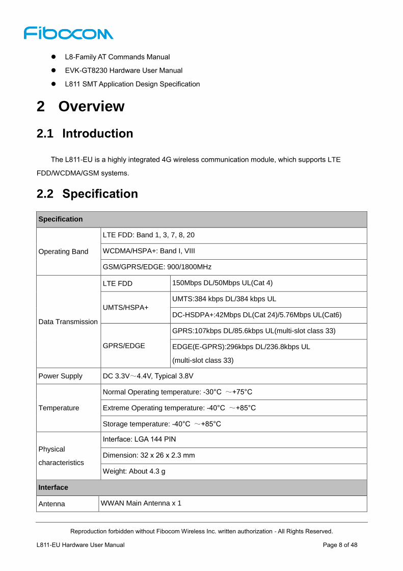
2 Overview
2.1 Introduction
The L811-EU is a highly integrated 4G wireless communication module, which supports LTE
FDD/WCDMA/GSM systems.
2.2 Specification
Specification
Operating Band
LTE FDD: Band 1, 3, 7, 8, 20
WCDMA/HSPA+: Band I, VIII
GSM/GPRS/EDGE: 900/1800MHz
Data Transmission
LTE FDD 150Mbps DL/50Mbps UL(Cat 4)
UMTS/HSPA+
UMTS:384 kbps DL/384 kbps UL
DC-HSDPA+:42Mbps DL(Cat 24)/5.76Mbps UL(Cat6)
GPRS/EDGE
GPRS:107kbps DL/85.6kbps UL(multi-slot class 33)
EDGE(E-GPRS):296kbps DL/236.8kbps UL
(multi-slot class 33)
Power Supply DC 3.3V~4.4V, Typical 3.8V
Temperature
Normal Operating temperature: -30°C ~+75°C
Extreme Operating temperature: -40°C ~+85°C
Storage temperature: -40°C ~+85°C
Physical
characteristics
Interface: LGA 144 PIN
Dimension: 32 x 26 x 2.3 mm
Weight: About 4.3 g
Interface
Antenna WWAN Main Antenna x 1

Reproduction forbidden without Fibocom Wireless Inc. written authorization - All Rights Reserved.
L811-EU Hardware User Manual Page 9 of 48
WWAN Diversity Antenna x 1
Function Interface
USIM 1.8V/3.0V
USB 2.0 x 1
4-line UART x 1
I2S
I2C
EINT、System Indicator
Clock
ADC x 1
JTAG/MIPI(Trace)
Software
Protocol Stack Embedded TCP/IP and UDP/IP protocol stack
AT commands 3GPP TS 27.007 and 27.005, and proprietary FIBOCOM AT commands
Firmware update USB
Note:
The RF performance of the module may be slightly beyond the 3GPP specifications when the
temperature exceeds the normal operating temperature range of -30°C~+75°C.
2.3 Application Framework
The peripheral applications for L811-EU module are shown in Figure 2-1:

Reproduction forbidden without Fibocom Wireless Inc. written authorization - All Rights Reserved.
L811-EU Hardware User Manual Page 10 of 48
Module
SIM USB
Power
Supply
VRTC VSD2_1V8
ON/OFF# RESET#
Control
EINT Indicator
Host application
UART
Main ANT
Main ANT
Div ANT
Div ANT
SIM
Card
Figure2-1 Application Framework
2.4 Hardware Framework
The hardware framework in Figure 2-2 shows the main hardware functions of L811-EU module, including
Baseband and RF functions.
Baseband contains the followings:
GSM/UMTS/LTE FDD controller/Power supply
Internal LPDDR2 RAM and NAND
Application interface
RF contains the followings:
RF Transceiver
RF Power/PA
RF Front end
RF Filter
Antenna

Reproduction forbidden without Fibocom Wireless Inc. written authorization - All Rights Reserved.
L811-EU Hardware User Manual Page 11 of 48
VBAT
POWER_ON/OFF#
RESET_N
VRTC
1V8
USB2.0
USIM
UART
EINT
INDICATOR
I2S
I2C
CLOCK
ADC
JTAG
MIPI
HSIC
Tunable ANT
Main ANT
Diversity ANT
Baseband(GSM/UMTS/LTE FDD controller)
PMU
TX
LPDDR2
RAM&
NAND
Div RF
Front
END
Main RF
Front
END
PA DCDC
PA
RF Transceiver
RX
RX
RF Part
TCXO
LG
A 1
44
PIN
In
terf
ac
e
Figure 2-2 Hardware Framework
3 Application Interface
3.1 LGA Interface
The L811-EU module applies LGA packaging, with a total of 144 pins.

Reproduction forbidden without Fibocom Wireless Inc. written authorization - All Rights Reserved.
L811-EU Hardware User Manual Page 12 of 48
3.1.1 Pin Distribution
Figure 3-1 Pin Distribution
Note:
Pin “NB” represents No ball, namely, no pin at this position.

Reproduction forbidden without Fibocom Wireless Inc. written authorization - All Rights Reserved.
L811-EU Hardware User Manual Page 13 of 48
3.1.2 Pin Definition
The pin definition is as follows:
Pin Pin Name I/O Reset Value Pin Description Type
USB2.0
A11 VBUS PI USB VBUS Supply 2.0---5.25V
A12 USB_DN IO T USB Data Minus 0.3---3.0V
A13 USB_DP IO T USB Data Plus 0.3---3.0V
SIM
D15 VSIM1 PO USIM power supply 1.8V/3.0V
E15 SIM1_RST O L USIM reset 1.8V/3.0V
F15 SIM1_CLK O L USIM clock 1.8V/3.0V
G15 SIM1_DATA IO L USIM data,internal pull up(4.7KΩ) 1.8V/3.0V
H15 SIM1_CD I T USIM detect, pull up(390KΩ)
High active 1.8V
F14 SIM1_DP IO PD USB data plus for USIM card
(not support now)
G14 SIM1_DN IO PD USB data minus for USIM card
(not support now)
UART1
A9 UART1_TXD O PU UART1 transmit Data CMOS 1.8V
A10 UART1_RXD I PD UART1 receive Data CMOS 1.8V
K14 UART1_RTS O PU UART1 Request To Send CMOS 1.8V
L14 UART1_CTS I PU UART1 Clear To Send CMOS 1.8V
EINT
J15 WAKEUP I L Wake up module CMOS 1.8V
K15 W_DISABLE# I L Disable WWAN CMOS 1.8V
H14 EINT3 I L ACM/MBIM interface switch
(Reserved) CMOS 1.8V
J14 BODY_SAR I L Body sar detect CMOS 1.8V
System Status Indicator
Reproduction forbidden without Fibocom Wireless Inc. written authorization - All Rights Reserved.
L811-EU Hardware User Manual Page 14 of 48
Pin Pin Name I/O Reset Value Pin Description Type
A4 CORE_DUMP O PD Core dump indicator CMOS 1.8V
A5 LPG O PD LPG indicator CMOS 1.8V
A7 WAKEUP_HOST O PD WAKEUP Host(AP) CMOS 1.8V
L15 PA_BLANKING/
TRIG_OUT O PD
PA blanking output/Monitoring Signal
Output CMOS 1.8V
I2S
N9 I2S2_WA0 O PD I2S L/R channel clock CMOS 1.8V
N10 I2S2_TX O PD I2S transmit data CMOS 1.8V
N11 I2S2_RX I PD I2S receive data CMOS 1.8V
N12 I2S2_CLK O PD I2S serial clock CMOS 1.8V
I2C
M11 I2C_SDA IO PU I2C serial data,pull up(4.7KΩ) CMOS 1.8V
M12 I2C_SCL O PU I2C serial clock,pull up(4.7KΩ) CMOS 1.8V
Clock
A3 FSYS2_26M O L 26MHz clock output,1.8V 1.8V
A8 CLK32K O PD 32kHz clock output,1.8V 1.8V
ADC
C10 ADC I General purpose A/D,1.2V max
voltage
ANT
J1 ANT_MAIN IO Main antenna
E1 ANT_DIV I Diversity antenna
ANT Tunable
B5 RFE_RFFE1_SDATA IO RFFE1 serial data for tunable ANT 1.8V
B4 RFE_RFFE1_SCLK O RFFE1 serial clock for tunable ANT 1.8V
B3 RFE_RFFE1_VIO PO RFFE1 VIO for tunable ANT 1.8V
HSIC(not support now)
B12 USB_HSIC_STRB IO High speed Inter IC clock
C12 USB_HSIC_DATA IO High speed Inter IC data
Reproduction forbidden without Fibocom Wireless Inc. written authorization - All Rights Reserved.
L811-EU Hardware User Manual Page 15 of 48
Pin Pin Name I/O Reset Value Pin Description Type
C4 IPC_HOST_WAKEUP O PU IPC host wakeup CMOS 1.8V
C5 IPC_TRIG_OUT O PD IPC trig out CMOS 1.8V
C7 IPC_TRIG_IN I PU IPC trig in CMOS 1.8V
C8 IPC_SLAVE_WAKEU
P I PD IPC slave wakeup CMOS 1.8V
NC
D13 NC Not connected
E13 NC Not connected
D14 NC Not connected
E14 NC Not connected
B13 NC Not connected
C13 NC Not connected
B14 NC Not connected
C14 NC Not connected
JTAG
L5 TDO O T Serial Data Out
M10 TDI I PU Serial Data Input
M7 TMS I PU State machine control signal
M9 TCK I PD JTAG clock input
M5 TRST_N I PD Reset/Module enable
M6 TRIG_IN I PD Monitoring Signal Input CMOS 1.8V
MIPI2 Trace
L7 MIPI2_TRC_CLK O PD MIPI2 trace clock CMOS 1.8V
L6 MIPI2_TRC_DATA0 IO PD MIPI2 trace data0 CMOS 1.8V
L9 MIPI2_TRC_DATA1 IO PD MIPI2 trace data1 CMOS 1.8V
L10 MIPI2_TRC_DATA2 IO PD MIPI2 trace data2 CMOS 1.8V
L11 MIPI2_TRC_DATA3 IO PD MIPI2 trace data3 CMOS 1.8V
Module Control
N7 RESET_N I Module reset input,pull up(100KΩ) 1.8V

Reproduction forbidden without Fibocom Wireless Inc. written authorization - All Rights Reserved.
L811-EU Hardware User Manual Page 16 of 48
Pin Pin Name I/O Reset Value Pin Description Type
N8 POWER_ON/OFF# I Module Power ON/OFF# signal,pull
down (200KΩ) 1.8V
Power
N3 VBAT PI - Power input Power supply
N4 VBAT PI - Power input Power supply
M3 VBAT PI - Power input Power supply
M4 VBAT PI - Power input Power supply
N5 VRTC PO - VRTC power supply Power supply
N6 VSD2_1V8 PO - 1.8V Power supply Power supply
B8 GND - - GND Power supply
B9 GND - - GND Power supply
B10 GND - - GND Power supply
B11 GND - - GND Power supply
C11 GND - - GND Power supply
F13 GND - - GND Power supply
L12 GND - - GND Power supply
M13 GND - - GND Power supply
L13 GND - - GND Power supply
G13 GND - - GND Power supply
H13 GND - - GND Power supply
J13 GND - - GND Power supply
K13 GND - - GND Power supply
A6 GND - - GND Power supply
B2 GND - - GND Power supply
B6 GND - - GND Power supply
B7 GND - - GND Power supply
C1 GND - - GND Power supply
C2 GND - - GND Power supply
C3 GND - - GND Power supply

Reproduction forbidden without Fibocom Wireless Inc. written authorization - All Rights Reserved.
L811-EU Hardware User Manual Page 17 of 48
Pin Pin Name I/O Reset Value Pin Description Type
C6 GND - - GND Power supply
C9 GND - - GND Power supply
C15 GND - - GND Power supply
D1 GND - - GND Power supply
D2 GND - - GND Power supply
D3 GND - - GND Power supply
D4 GND - - GND Power supply
D12 GND - - GND Power supply
E2 GND - - GND Power supply
E3 GND - - GND Power supply
F1 GND - - GND Power supply
F2 GND - - GND Power supply
F3 GND - - GND Power supply
G1 GND - - GND Power supply
G2 GND - - GND Power supply
G3 GND - - GND Power supply
H1 GND - - GND Power supply
H2 GND - - GND Power supply
H3 GND - - GND Power supply
J2 GND - - GND Power supply
J3 GND - - GND Power supply
K1 GND - - GND Power supply
K2 GND - - GND Power supply
K3 GND - - GND Power supply
K4 GND - - GND Power supply
K12 GND - - GND Power supply
L1 GND - - GND Power supply
L2 GND - - GND Power supply

Reproduction forbidden without Fibocom Wireless Inc. written authorization - All Rights Reserved.
L811-EU Hardware User Manual Page 18 of 48
Pin Pin Name I/O Reset Value Pin Description Type
L3 GND - - GND Power supply
L4 GND - - GND Power supply
L8 GND - - GND Power supply
M2 GND - - GND Power supply
M8 GND - - GND Power supply
M14 GND - - GND Power supply
N13 GND - - GND Power supply
A1 GND - - GND Power supply
A15 GND - - GND Power supply
N1 GND - - GND Power supply
N15 GND - - GND Power supply
TG1 GND - - Thermal Ground -
TG2 GND - - Thermal Ground -
TG3 GND - - Thermal Ground -
TG4 GND - - Thermal Ground -
TG5 GND - - Thermal Ground -
TG6 GND - - Thermal Ground -
TG7 GND - - Thermal Ground -
TG8 GND - - Thermal Ground -
TG9 GND - - Thermal Ground -
TG10 GND - - Thermal Ground -
TG11 GND - - Thermal Ground -
TG12 GND - - Thermal Ground -
TG13 GND - - Thermal Ground -
TG14 GND - - Thermal Ground -
TG15 GND - - Thermal Ground -
TG16 GND - - Thermal Ground -

Reproduction forbidden without Fibocom Wireless Inc. written authorization - All Rights Reserved.
L811-EU Hardware User Manual Page 19 of 48
H: High Voltage Level
L: Low Voltage Level
PD: Pull-Down
PU: Pull-Up
T: Tristate
OD: Open Drain
PP: Push-Pull
Note:
The unused pins can be left floating.
3.2 Power Supply
The power interface of L811-EU module as shown in the following table:
Pin Pin Name I/O Pin Description
DC Parameter (V)
Minimum
Value
Typical
Value
Maximum
Value
N3,N4,M3,M4 VBAT PI Power input 3.3 3.8 4.4
A11 VBUS PI USB power supply 2.0 3.8 5.25
N5 VRTC PO VRTC power supply 1.71 1.8 1.89
N6 VSD2_1V8 PO 1.8V power supply 1.71 1.8 1.89
D15 VSIM1 PO SIM1 power supply 1.8V/3.0V
3.2.1 Power Supply
The L811-EU module should be powered through the VBAT pins, and the power supply design is shown
in Figure 3-2:

Reproduction forbidden without Fibocom Wireless Inc. written authorization - All Rights Reserved.
L811-EU Hardware User Manual Page 20 of 48
Figure 3-2 Power Supply Design
The filter capacitor design for power supply is shown in the following table:
Recommended
capacitance Application Description
220uF x 2 Capacitor for steady voltage
Reduce power fluctuations of the module in
operation, requiring capacitor with low ESR
LDO or DCDC power supply requires the
capacitor of no less than 440uF
The capacitor for battery power supply
can be reduced to 100~220uF
1uF, 100nF Digital signal noise Filter out the interference generated from the
clock and digital signals
39pF, 33pF 700/850/900 MHz frequency
band Filter out low frequency band RF interference
18pF, 8.2pF,
6.8pF
1700/1800/1900/2100/2500/
2600MHz frequency band
Filter out medium/high frequency band RF
interference
The stable power supply can ensure the normal operation of L811-EU module, and the ripple of the power
supply should be less than 300mV in design. When the module operates under GSM mode (Burst
transmit), the maximum operating current can reach 2A, so the power source should be not lower than
3.3V, or the module may shut down or reboot. The power supply limits are shown in Figure 3-3:

Reproduction forbidden without Fibocom Wireless Inc. written authorization - All Rights Reserved.
L811-EU Hardware User Manual Page 21 of 48
Figure 3-3 Power Supply Limits
3.2.2 RTC Power Supply
The VRTC is the power supply for the RTC inside the module and it can be used as the backup power
supply for the RTC. When the module is powered up by supplying the VBAT power, the VRTC will output
1.8V voltage. The VRTC parameters are as follows:
Parameters Minimum Value Typical Value Maximum Value Unit
VRTC output voltage 1.71 1.8 1.89 V
VRTC input voltage
(normal clock) 1.0 1.8 1.89 V
VRTC input current
(normal clock) 10 20 uA
The reference design circuit for VRTC as the backup power supply for RTC is shown in Figure 3-4:
Figure3-4 VRTC Reference Design Circuit
Instructions for VRTC (which works as the backup power supply for RTC):
R1 is a current limiting resistor, which is used to limit the charging current for VRTC, and the
recommended resistance value is 10KΩ.
Burst transmit Burst transmit
min:3.3V
VBATRipple≤300mV
Drop
VBAT≥3.3V

Reproduction forbidden without Fibocom Wireless Inc. written authorization - All Rights Reserved.
L811-EU Hardware User Manual Page 22 of 48
Current consumption for VRTC is about 10uA.
C1 value will affect the sustaining time for RTC clock after VBAT outage, and the sustaining time for
RTC can refer to the following formula: T = (1.8-1.0) * C / 10 = 0.08C, the unit is “second”. That is, if
C1 uses a 100uF capacitor, and the sustaining time for the RTC is approximately 8s.
If there is no need for the module clock backup feature, VRTC pin can be left floating.
3.2.3 1.8V Power Supply
The L811-EU module provides 1.8V power supply through VSD2_1V8 for the digital circuits in the module,
and the voltage is the logical voltage level for the module, which can be used to indicate the start-up
status of the module and can also be used for circuit application of external low current (<50mA), and can
be left floating if not used. The definition for the logical voltage level of VSD2_1V8 is as follows:
Parameters Minimum Value Typical Value Maximum Value Unit
VSD2_1V8 1.71 1.8 1.89 V
VIH 1.3 1.8 1.89 V
VIL -0.3 0 0.5 V
3.2.4 Power Consumption
In the case of 3.8V power supply, the power consumption for L811-EU module is shown in the following
table:
Parameter Mode Condition Typical
Current(mA)
Ioff Power off Power supply,module power off 0.086
IIdle
GSM MFRMS=5 12
WCDMA DRX=8 11.8
LTE FDD Paging cycle #256 frames (2.56 sec DRx cycle) 12
ISleep
GSM
MFRMS=2 3.6
MFRMS=5 3.2
MFRMS=9 2.7
WCDMA DRX=6 2.8
DRX=8 2.5
Reproduction forbidden without Fibocom Wireless Inc. written authorization - All Rights Reserved.
L811-EU Hardware User Manual Page 23 of 48
Parameter Mode Condition Typical
Current(mA)
DRX=9 2.2
LTE FDD Paging cycle #64 frames (0.64 sec DRx cycle) 2.2
Radio Off AT+CFUN=4,Flight mode 2.0
IGSM-RMS GSM voice
GSM900 PCL5 210
DCS1800 PCL0 155
IGPRS-RMS
CS4 GPRS
GPRS Data transfer GSM900; PCL=5; 1Rx/4Tx 600
GPRS Data transfer DCS1800; PCL=0; 1Rx/4Tx 450
IEGPRS-RMS
MCS9 EDGE
EDGE Data transfer GSM900; PCL=8; 1Rx/4Tx 420
EDGE Data transfer DCS1800; PCL=2; 1Rx/4Tx 405
IWCDMA-RMS WCDMA
WCDMA Data transfer Band I @+23.5dBm 550
WCDMA Data transfer Band VIII @+23.5dBm 510
ILTE-RMS LTE FDD
LTE FDD Data transfer Band 1 @+23dBm 570
LTE FDD Data transfer Band 3 @+23dBm 570
LTE FDD Data transfer Band 7 @+23dBm 650
LTE FDD Data transfer Band 8 @+23dBm 595
LTE FDD Data transfer Band 20 @+23dBm 560
3.3 Control Signal
The L811-EU module provides two control signals for power on/off and reset operations, the pin defined
as shown in the following table:
Pin Pin Name I/O Reset Value Functions Type
N8 POWER_ON/OFF# I
Power on/off signal, internal pull down
(200KΩ)
High: Power on
Low or floating: Power off
1.8V
N7 RESET_N I Reset signal with 100KΩ internal pull
up, active low. 1.8V

Reproduction forbidden without Fibocom Wireless Inc. written authorization - All Rights Reserved.
L811-EU Hardware User Manual Page 24 of 48
3.3.1 Module Start-Up
3.3.1.1 Start-up Circuit
The VRTC output from the module can be used as the pull up voltage.
AP (Application Processor) controls the module start-up, and the circuit design is shown in Figure
3-5:
Figure 3-5 Circuit for Module Start-up Controlled by AP
3.3.1.2 Start-up Timing Sequence
After powering on, the module will start-up by pulling up the POWER_ON/OFF# signal for more than
20ms (100ms recommended). Meanwhile, the VSD2_1V8 will output 1.8V voltage, and the module
begins the start-up initialization process. The start-up timing is shown in Figure 3-6:
Figure 3-6 Start-up Timing Sequence
20ms
VBAT
POWER_ON/OFF#
VSD2_1V8
1s
RESET_N
100ms
Module State OFF Initialization Activation(AT Command Ready)
10s
Reproduction forbidden without Fibocom Wireless Inc. written authorization - All Rights Reserved.
L811-EU Hardware User Manual Page 25 of 48
Note:
RESET_N is required to pull high with a 1s delay after the VBAT, because it takes some time for
the voltage supplied to VBAT (capacitor charging). If the power supply for VBAT remains before
the module starting up, the delay time can be ignored.
3.3.2 Module Shutdown
The module can be shut down by software or hardware control:
Shutdown Control Action Condition
Software Sending AT+CPWROFF
command Normal shutdown.
Hardware Pull down Power_ON/OFF# pin Only used when a hardware exception occurs
and the software control can not be used
3.3.2.1 Software Shutdown
The module can be shut down by sending AT+CPWROFF command.
When the module receives the software shutdown command (AT+CPWROFF), the module will start the
finalization process (the reverse process of initialization), and it will be completed after 3s. In the
finalization process, the module will save the network, SIM card and some other parameters from memory,
then clear the memory and PMU will be powered off. After shutdown, the VSD2_1V8 voltage is also shut
down. The software control timing is shown in Figure 3-7:
VBAT
POWER_ON/OFF#
VSD2_1V8AT+CPWROFF
Module State Activation Finalization OFF
2s
RESET_N
Figure 3-7 Software Shutdown Timing Control
After the software shutdown, the POWER_ON/OFF# pin will remain high which prevents the module from
restarting again. To enable the next restart, the POWER_ON/OFF# pin should be pulled low after shutting
down.

Reproduction forbidden without Fibocom Wireless Inc. written authorization - All Rights Reserved.
L811-EU Hardware User Manual Page 26 of 48
3.3.2.2 Hardware Shutdown
By pulling down POWER_ON/OFF# pin for more than 10ms (100ms recommended), the power
management unit (PMU) of the module loses its power, and then the module will shut down by hardware.
Because the PMU will lose its power by pulling down the POWER_ON/OFF# pin, to avoid damaging the
module with power on/off procedures, it’s necessary to pull down RESET_N pin for 100ms before pulling
down the POWER_ON/OFF# pin. The hardware control timing is shown in Figure 3-8:
VBAT
POWER_ON/OFF#
VSD2_1V8
Module State Activation PMU RESET OFF
10ms
RESET_N
100ms
Figure 3-8 Hardware Control Timing
3.3.3 Module Reset
The module supports the reset function, and the module can be reset to the initial status by pulling down
the RESET_N signal for more than 10ms (100ms recommended), and the module will restart after the
RESET_N signal is released. When the customer executes RESET_N function, the PMU remains its
power inside the module. The recommended circuit design is shown in the Figure 3-9:
Figure 3-9 Recommended Design for Reset Circuit
The RESET control timing is shown in Figure 3-10:

Reproduction forbidden without Fibocom Wireless Inc. written authorization - All Rights Reserved.
L811-EU Hardware User Manual Page 27 of 48
Figure 3-10 Reset Control Timing
Note:
RESET_N is a sensitive signal, so it’s recommended to add a filter capacitor nearby the module.
In case of PCB layout, the RESET_N signal lines should keep away from the RF interference
and be protected by GND. Also, the RESET_N signal lines shall neither near the PCB edge nor
route on the surface planes to avoid module from reset caused by ESD.
3.4 USB Interface
The L811-EU module supports USB 2.0 which is compatible with USB High-Speed (480 Mbit/s) and USB
Full-Speed (12 Mbit/s). For the USB timing and electrical specification of L811-EU module, please refer to
“Universal Serial Bus Specification 2.0”.
3.4.1 USB Interface Definition
Pin# Pin Name I/O Reset Value Description Type
A11 VBUS PI USB power supply 2.0---5.25V
A12 USB_DN IO T USB Data Minus 0.3---3.0V
A13 USB_DP IO T USB Data Plus 0.3---3.0V
The VBUS power supply is used for the detection of the USB port, after VBUS is powered on, the USB
function of the module will be enabled and the enumeration will begin. The VBUS is only used for the
detection of USB port, and the current supplied is about 1mA. When USB_DN & USB_DP are
disconnected, the module will not enter sleep mode if VBUS power is supplied.
The corresponding USB driver shall be installed before the L811-EU module is used on the PC with Win7
system (kernel driver should be configured for Android/Linux system). After the module is inserted into PC
with Win7 system, the USB driver will map 3 COM ports and 1 NCM ports, which are described as follows:
VBAT
POWER_ON/OFF#
VSD2_1V8
Module State Activation PMU RESET
10ms
RESET_N 100ms
Restart Activation
10s

Reproduction forbidden without Fibocom Wireless Inc. written authorization - All Rights Reserved.
L811-EU Hardware User Manual Page 28 of 48
2 COM ports can be used to send AT Commands.
1 COM port can be used to capture LOG information with debugging software.
1 NCM port is virtual network port, which can be used to initiate the data service.
Note:
One COM port can be used as the Modem COM port to initiate the data service. Since the speed of
the Modem COM port is not sufficient for the 150 Mbit/s peak downlink speed requirement for LTE,
so it is not recommended to be used.
3.4.2 USB Interface Application
The reference circuit is shown in Figure 3-11:
Figure3-11 Reference Circuit for USB Interface
Since the module supports USB 2.0 High-Speed, it is required to use TVS diodes with equivalent
capacitance of 1pF or smaller ones on the USB_DN/DP differential signal lines, it is recommended to use
0.5pF TVS diodes. There is no special requirements for TVS diodes on VBUS pin, normally the 8 ~ 10pF
TVS diodes can be used.
USB_DN and USB_DP are high speed differential signal lines with the maximum transfer rate of 480
Mbit/s, so the following rules shall be followed carefully in the case of PCB layout:
USB_DN and USB_DP signal lines should have the differential impedance of 90 ohms.
USB_DN and USB_DP signal lines should be parallel and have the equal length, the right angle
routing should be avoided.
USB_DN and USB_DP signal lines should be routed on the layer that is next to the ground layer,
and wrapped with GND on both sides and layers.

Reproduction forbidden without Fibocom Wireless Inc. written authorization - All Rights Reserved.
L811-EU Hardware User Manual Page 29 of 48
3.5 USIM Interface
The L811-EU module has a built-in USIM card interface, which supports 1.8V and 3.0V SIM cards.
3.5.1 USIM Pins
The USIM pins are described as follows:
Pin Pin Name I/O Reset Value Pin Description Type
D15 VSIM1 PO USIM power supply 1.8V/3.0V
E15 SIM1_RST O L USIM reset 1.8V/3.0V
F15 SIM1_CLK O L USIM clock 1.8V/3.0V
G15 SIM1_DATA IO L USIM data, internal pull up(4.7KΩ) 1.8V/3.0V
H15 SIM1_CD I T
USIM card detect, pull up(390KΩ)
Active-high, and high level means
SIM card is inserted, and low level
means SIM card is detached.
1.8V
3.5.2 USIM Interface Circuit
3.5.2.1 N.C. SIM Card Slot
The reference circuit design for N.C. (Normally Closed) SIM card slot is shown in Figure 3-12:
Figure 3-12 Reference Circuit for N.C. SIM Card Slot
The principles of the N.C. SIM card slot are described as follows:
When the SIM card is detached, it connects the short circuit between CD and SW pins, and drives the
SIM1_CD pin low.
Reproduction forbidden without Fibocom Wireless Inc. written authorization - All Rights Reserved.
L811-EU Hardware User Manual Page 30 of 48
When the SIM card is inserted, it connects an open circuit between CD and SW pins, and drives the
SIM1_CD pin high.
3.5.2.2 N.O. SIM card slot
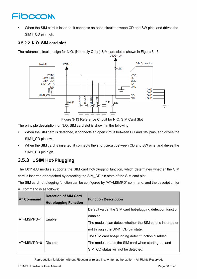
The reference circuit design for N.O. (Normally Open) SIM card slot is shown in Figure 3-13:
Figure 3-13 Reference Circuit for N.O. SIM Card Slot
The principle description for N.O. SIM card slot is shown in the following:
When the SIM card is detached, it connects an open circuit between CD and SW pins, and drives the
SIM1_CD pin low.
When the SIM card is inserted, it connects the short circuit between CD and SW pins, and drives the
SIM1_CD pin high.
3.5.3 USIM Hot-Plugging
The L811-EU module supports the SIM card hot-plugging function, which determines whether the SIM
card is inserted or detached by detecting the SIM_CD pin state of the SIM card slot.
The SIM card hot-plugging function can be configured by “AT+MSMPD” command, and the description for
AT command is as follows:
AT Command Detection of SIM Card
Hot-plugging Function Function Description
AT+MSMPD=1 Enable
Default value, the SIM card hot-plugging detection function
enabled.
The module can detect whether the SIM card is inserted or
not through the SIM1_CD pin state.
AT+MSMPD=0 Disable
The SIM card hot-plugging detect function disabled.
The module reads the SIM card when starting up, and
SIM_CD status will not be detected.

Reproduction forbidden without Fibocom Wireless Inc. written authorization - All Rights Reserved.
L811-EU Hardware User Manual Page 31 of 48
After the SIM card hot-plugging detection function is enabled, when the SIM1_CD is high level, the
module detects that the SIM card is inserted, and then executes the initialization program, and finish the
network registration after reading the SIM card information. When the SIM1_CD is low level, the module
determines that the SIM card is detached, and does not read the SIM card.
Note:
By default, SIM_CD is active-high, which can be switched to active-low by AT command. Please
refer to the AT Commands Manual for the AT command.
3.5.4 USIM Design
The SIM card circuit design shall meet the EMC standards and ESD requirements with the improved
capability to resist interference, to ensure that the SIM card can work stably. The following guidelines
should be noted in case of design:
The SIM card slot placement should near the module as close as possible, and away from the
RF antenna, DC/DC power supply, clock signal lines, and other strong interference sources.
The SIM card slot with a metal shielding housing can improve the anti-interference ability.
The trace length between the SIM card slot and the module should not exceed 100mm, or it
could reduce the signal quality.
The SIM1_CLK and SIM1_DATA signal lines should be isolated by GND to avoid crosstalk
interference. If it is difficult for the layout, the whole SIM signal lines should be wrapped with
GND as a group at least.
The filter capacitors and ESD devices for SIM card signals should be placed near to the SIM
card slot, and the ESD devices with 22~33pF capacitance should be used.
3.6 UART Interface
3.6.1 UART Interface Definition
The L811-EU module provides one 4-line UART port for asynchronous serial communication. The UART
port supports AT commands, which allows the users to receive and transmit AT commands.
The definition of the UART port is as follows:
Pin Pin Name I/O Reset Value Pin Description Type
A9 UART1_TXD O PU UART1 transmit Data CMOS 1.8V
A10 UART1_RXD I PD UART1 receive Data CMOS 1.8V
Reproduction forbidden without Fibocom Wireless Inc. written authorization - All Rights Reserved.
L811-EU Hardware User Manual Page 32 of 48
K14 UART1_RTS O PU UART1 Request To Send CMOS 1.8V
L14 UART1_CTS I PU UART1 Clear To Send CMOS 1.8V
3.6.2 UART Interface Application
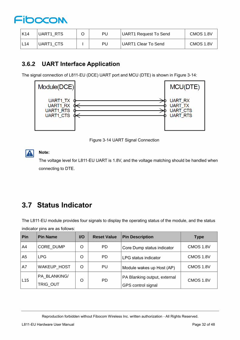
The signal connection of L811-EU (DCE) UART port and MCU (DTE) is shown in Figure 3-14:
Figure 3-14 UART Signal Connection
Note:
The voltage level for L811-EU UART is 1.8V, and the voltage matching should be handled when
connecting to DTE.
3.7 Status Indicator
The L811-EU module provides four signals to display the operating status of the module, and the status
indicator pins are as follows:
Pin Pin Name I/O Reset Value Pin Description Type
A4 CORE_DUMP O PD Core Dump status indicator CMOS 1.8V
A5 LPG O PD LPG status indicator CMOS 1.8V
A7 WAKEUP_HOST O PU Module wakes up Host (AP) CMOS 1.8V
L15 PA_BLANKING/
TRIG_OUT O PD
PA Blanking output, external
GPS control signal CMOS 1.8V
Reproduction forbidden without Fibocom Wireless Inc. written authorization - All Rights Reserved.
L811-EU Hardware User Manual Page 33 of 48
3.7.1 CORE DUMP
The CORE_DUMP signal is used to indicate the software restarting caused by the abnormal operation.
When the module is working abnormally, the software will restart the module, and one virtual ACM port
will be generated after restarting the module, then the CORE_DUMP signal will be changed from low level
to high level.
Module Status CORE_DUMP Signal
Normal mode Low level
Core Dump High level
Note:
The Core dump indication function is disabled by default, and it can be enabled by the AT
command.
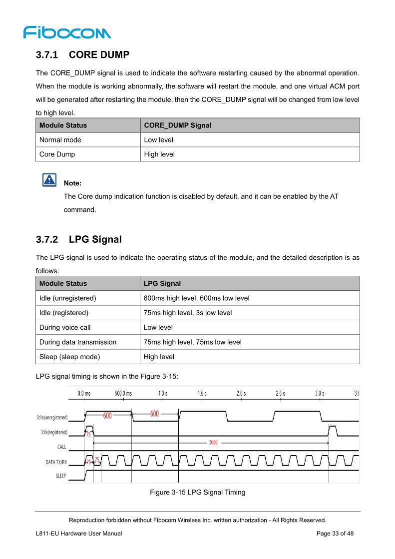
3.7.2 LPG Signal
The LPG signal is used to indicate the operating status of the module, and the detailed description is as
follows:
Module Status LPG Signal
Idle (unregistered) 600ms high level, 600ms low level
Idle (registered) 75ms high level, 3s low level
During voice call Low level
During data transmission 75ms high level, 75ms low level
Sleep (sleep mode) High level
LPG signal timing is shown in the Figure 3-15:
Figure 3-15 LPG Signal Timing

Reproduction forbidden without Fibocom Wireless Inc. written authorization - All Rights Reserved.
L811-EU Hardware User Manual Page 34 of 48
3.7.3 WAKEUP_HOST
The WAKEUP_HOST signal is used to wake the Host (AP) when there are incoming calls, SMS or other
data requests. The definition of WAKEUP_HOST signal is as follows:
Operating Mode WAKEUP_HOST Signal
Ringing /SMS or data requests Pull low 1s then Pull high(pulse signal)
Idle/Sleep High level
WAKEUP_HOST timing is shown in Figure 3-16:
Figure 3-16 WAKEUP_HOST Timing
3.7.4 PA_BLANKING
While the module works in GSM frequency band, the PA_BLANKING pin will output the pulse signals that
synchronize with the GSM burst TX timing.
As the GSM TX may interfere the receiving of the GPS signal, AP can disable GPS or stop receiving GPS
data when it detects the PA_BLANKING pulse signals, to avoid GPS working abnormally.
Operating modes PA_BLANKING signal
Default Low level
GSM burst TX Output the pulse signals that synchronize with the GSM burst TX
PA_BLANKING timing is shown in Figure 3-17:
Figure 3-17 PA_BLANKING Timing
WAKEUP_HOST
1S
Idle/Sleep Call/SMS/Data Idle/SleepStatus
Burst transmit Burst transmit
PA_BLANKING
Burst transmit
about 4.615ms
about 577us

Reproduction forbidden without Fibocom Wireless Inc. written authorization - All Rights Reserved.
L811-EU Hardware User Manual Page 35 of 48
3.8 Interrupt Control
The L811-EU module provides three interrupt signals, and the pin definition is as follows:
Pin Pin Name I/O Reset Value Pin Description Type
J15 WAKEUP I PD AP wakes up module CMOS 1.8V
K15 W_DISABLE# I PD Enable/Disable RF network CMOS 1.8V
J14 BODY_SAR I PU Body SAR detection CMOS 1.8V
3.8.1 WAKEUP
The L811-EU module provides an additional interrupt port to wake up the module. In the case of using
USB interface, according to the USB protocol, the module can be waken up by the USB. But in the case
of using the serial port, the WAKEUP pin needs to be pulled down to wake up the module from sleep
mode. The definition of the WAKEUP signal is as follows:
Module
status WAKEUP signal Operating mode
Sleep High level The module keeps Sleep status.
Low level Wake up module, the status is changed from Sleep to Idle.
Idle High level
The module keeps in Idle status and automatically enters the sleep
status after several seconds.
Low level The module keeps in Idle status and will not enter the sleep status.
WAKEUP timing is shown in Figure 3-18:
WAKEUP
Sleep Idle SleepStatus Idle
Figure 3-18 WAKEUP Timing
3.8.2 W_DISABLE#
The module provides a hardware pin to enable/disable WWAN RF function, and the function can also be
controlled by the AT command. The module enters the Flight mode after the RF function is disabled. The
definition of W_DISABLE# signal is as follows:

Reproduction forbidden without Fibocom Wireless Inc. written authorization - All Rights Reserved.
L811-EU Hardware User Manual Page 36 of 48
3.8.3 BODY_SAR
The L811-EU module supports the BODY_SAR detection function. The voltage level is high by default for
BODY_SAR, and when the SAR sensor detects the closing human body, the BODY_SAR signal will be
pulled down by AP. As the result, the module then lowers down its emission power to its default threshold
value, reducing RF radiation to the human body. The threshold of emission power can be set by the AT
Commands. The definition for BODY_SAR function is as follows:
No. BODY_SAR signal Function
1 High/Floating The module keeps the default emission power
2 Low Lower the maximum emission power to the threshold value of the
module.
3.9 Digital Audio
The L811-EU module supports I2S digital audio interface and it supports the ordinary I2S mode and PCM
mode. The signal level of the I2S interface is 1.8V. Please refer to “FIBOCOM Digital Voice” description
for detailed application design.
The definition of I2S signals is as follows:
Pin Pin Name I/O Reset Value Pin Description Type
N9 I2S2_WA0 O PD I2S left and right channel clock
(LRCK) CMOS 1.8V
N10 I2S2_TX O PD I2S data transmit CMOS 1.8V
N11 I2S2_RX I PD I2S data receive CMOS 1.8V
N12 I2S2_CLK O PD I2S clock CMOS 1.8V
No. W_DISABLE# signal Function
1 High/Floating WWAN enable, the module exits the Flight mode.
2 Low WWAN disable, the module enters the Flight mode.

Reproduction forbidden without Fibocom Wireless Inc. written authorization - All Rights Reserved.
L811-EU Hardware User Manual Page 37 of 48
3.9.1 I2S Mode
The L811-EU module is connected to the audio codec via I2S, and the codec encodes the audio data to
implement the voice call function. At this point, the module works as the I2S master, and the codec works
as the I2S slave. I2S signal connection is shown in Figure 3-19:
Figure 3-19 I2S Signal Connection
Description:
I2S interface can be configured as master or slave mode.
It supports multiple audio sampling rates (44.1KHz,32KHz,24KHz,16KHz,8KHz).
It supports 16bit and 32bit mode.
3.9.2 PCM Mode
In the case of the Bluetooth (BT) call, the PCM mode is used to transmit digital voice data if the BT chip
does not support I2S. At this point, the module works as the PCM master, and BT works as the PCM slave
mode. The signal connection under the PCM mode is shown in Figure 3-20:
Figure 3-20 Signal Connection in PCM Mode
Description:
The PCM mode interface can be configured as master or slave mode.
It supports various audio sampling rates (44.1KHz,32KHz,24KHz,16KHz,8KHz).
It supports short frame sync for 16 and 32 bit mode.
It supports burst and continuous transmission modes.
It supports clock length trigger for frame sync signal and rising/falling edge trigger for data
transmission.

Reproduction forbidden without Fibocom Wireless Inc. written authorization - All Rights Reserved.
L811-EU Hardware User Manual Page 38 of 48
Note:
PCM mode timing is relative complicated to adjust, and the audio quality will be effected when
not fine tuned. In contrast to PCM mode, I2S mode is easier to adjust, hence it is recommended
to use I2S mode.
3.10 I2C Interface Description
The L811-EU module supports one I2C interface, which is configured as I2C master by default. The I2C
master is used for driving external I2C slave devices, such as the audio codec.
Pin Pin Name I/O Reset Value Pin Description Type
M11 I2C_SDA IO PU I2C serial data, internal pull up
(4.7KΩ) CMOS 1.8V
M12 I2C_SCL O PU I2C serial clock, internal pull up
(4.7KΩ) CMOS 1.8V
The module is connected to the external I2C slave devices (e.g. Audio Codec), which is as follows:
Figure 3-21 I2C Signal Connection
Note:
I2C interface can be left floating if not used.
3.11 Clock Interface
The L811-EU module supports two clocks, they can output 26MHz and 32KHz clocks respectively.
Pin Pin Name I/O Reset Value Pin Description Type
A3 FSYS2_26M O L 26M clock output, 1.8V
(used for external GPS or Audio Codec) 1.8V
A8 CLK32K O PD 32K clock output, 1.8V 1.8V

Reproduction forbidden without Fibocom Wireless Inc. written authorization - All Rights Reserved.
L811-EU Hardware User Manual Page 39 of 48
3.12 ADC Interface
The L811-EU module supports ADC detection, and the value of the analog voltage can be read by the
AT+MMAD command. The ADC input voltage range is 0 ~ 1.2V, and the precision reaches 10bit. The
ADC signal description is as follows:
Pin Pin Name I/O Reset Value Pin Description Type
C10 ADC I General purpose A/D,1.2V max voltage
3.13 Other Interfaces
The module does not support the following ports yet: HSIC, ANT Tunable.
Reproduction forbidden without Fibocom Wireless Inc. written authorization - All Rights Reserved.
L811-EU Hardware User Manual Page 40 of 48
4 RF Interface
4.1 Operating Band
The L811-EU module provides main and diversity antenna interfaces, main is used to transmit and
receive RF signals, and the diversity is used to receive RF signals. The operating bands of the antennas
are as follows:
Operating Band
Description Mode Tx (MHz) Rx (MHz)
Band 1 2100MHz LTE FDD/WCDMA 1920 - 1980 2110 - 2170
Band 3 1800MHz LTE FDD/GSM 1710 - 1785 1805 - 1880
Band 7 2600MHz LTE FDD 2500 - 2570 2620 -2690
Band 8 900MHz LTE FDD/WCDMA/GSM 880 - 915 925 - 960
Band 20 800MHz LTE FDD 832 - 862 791 - 821
4.2 Transmitting Power
The transmitting power for each band of the L811-EU module is as follows:
Mode Band Tx Power(dBm)
3GPP Tx Power(dBm)
Typical Note
GSM GSM 900 33±2 32.5±1
DCS 1800 30±2 29.5±1
WCDMA Band I 23±2.7 23.5±1
Band VIII 23±2.7 23.5±1
LTE FDD
Band 1 23±2.7 23±1 10MHz Bandwidth, 1 RB
Band 3 23±2.7 23±1 10MHz Bandwidth, 1 RB
Band 7 23±2.7 23±1 10MHz Bandwidth, 1 RB
Band 8 23±2.7 23±1 10MHz Bandwidth, 1 RB
Band 20 23±2.7 23±1 10MHz Bandwidth, 1 RB

Reproduction forbidden without Fibocom Wireless Inc. written authorization - All Rights Reserved.
L811-EU Hardware User Manual Page 41 of 48
4.3 Receiver Sensitivity
The receiving sensitivity for each band of the L811-EU module is as follows:
Mode Band Rx Sensitivity(dBm)
3GPP Rx Sensitivity(dBm)
Typical Note
GSM GSM 900 -102 -108.5 BER<2.43%
DCS 1800 -102 -108.5 BER<2.43%
WCDMA Band I -106.7 -111 BER<0.1%
Band VIII -103.7 -111 BER<0.1%
LTE FDD
Band 1 -96.3 -101.5 10MHz Band width
Band 3 -93.3 -101.5 10MHz Band width
Band 7 -94.3 -101 10MHz Band width
Band 8 -93.3 -102.5 10MHz Band width
Band 20 -93.3 -101 10MHz Band width
Note:
The above values are measured for the dual antennas situation (Main + Diversity). For single
main antenna (without Diversity), the sensitivity will drop around 3dB for each band of LTE.
4.4 RF PCB Design
4.4.1 Trace Routing Principle
The L811-EU module supports dual antennas, which meets the requirements for LTE of 3GPP. The
MAIN_ANT is used to transmit and receive RF signals, while the DIV_ANT is used to receive RF signals.
Using diversity antenna to improve the receiving sensitivity of RF antenna and double the download rate.
Since L811-EU is an LTE module, dual antennas should be applied to meet the performance
requirements.
The L811-EU module does not provide RF connector itself, so routing RF trace is required for the
connection with RF connectors or antenna feed points on the application mainboard. It is recommended
to use the microstrip line for RF trace, with the insertion loss controlled within 0.2dB and impedance
controlled at 50Ω.
It is recommended to reserve a π circuit (the parallel inductors should connect to the RF trace) between
the L811-EU module and the antenna connectors (or the feed points). The parallel devices are directly
across the RF lines and no branch is allowed.

Reproduction forbidden without Fibocom Wireless Inc. written authorization - All Rights Reserved.
L811-EU Hardware User Manual Page 42 of 48
0R
0R
NC NC
NC NC
Module
ANT_MAIN
ANT_DIV
Main Antenna
Div Antenna
Figure 4-1 L811-EU Antenna π Circuit
4.4.2 Impedance Design
The impedance of the RF traces of the antenna interface shall be controlled at 50Ω.

Reproduction forbidden without Fibocom Wireless Inc. written authorization - All Rights Reserved.
L811-EU Hardware User Manual Page 43 of 48
4.5 Antenna Design
4.5.1 Antenna Design Requirements
The L811-EU module provides main and diversity antenna interfaces, and the antenna design
requirements are as follows:
Main antenna requirements for L811-EU module
Frequency range The most proper antenna to adapt the frequencies should be used.
Bandwidth
(GSM/EDGE)
GSM900 : 80 MHz
GSM1800(DCS) : 170 MHz
Bandwidth
(WCDMA)
WCDMA band I(2100) : 250 MHz
WCDMA band VIII(900) : 80 MHz
Bandwidth
(LTE)
LTE band 1(2100): 250 MHz
LTE Band 3(1800): 170 MHz
LTE band 7(2600): 190 MHz
LTE Band 8(900): 80 MHz
LTE band 20(800): 71 MHz
Impedance 50Ω
Input power > 33dBm(2 W) peak power GSM
> 23dBm average power WCDMA & LTE
Recommended
standing-wave ratio
(SWR)
≤ 2:1

Reproduction forbidden without Fibocom Wireless Inc. written authorization - All Rights Reserved.
L811-EU Hardware User Manual Page 44 of 48
5 Structure Specification
5.1 Product Appearance
The product appearance for L811-EU module is shown in Figure 5-1:
Figure 5-1 Module Appearance
5.2 Dimension of Structure
The structural dimension of the L811-EU module is shown in Figure 5-2:
Figure 5-2 Dimension of Structure(Unit:mm)

Reproduction forbidden without Fibocom Wireless Inc. written authorization - All Rights Reserved.
L811-EU Hardware User Manual Page 45 of 48
5.3 Recommended Design for PCB Bonding Pad
Figure5-3 Recommended Design for PCB Bonding Pad (Unit: mm)
5.4 SMT
For the design of SMT stencil, solder paste, and the furnace temperature control, please refer to the SMT
Application Design Specification.
Reproduction forbidden without Fibocom Wireless Inc. written authorization - All Rights Reserved.
L811-EU Hardware User Manual Page 46 of 48
5.5 Storage
5.5.1 Storage Life
Storage Conditions (recommended): Temperature is 23 ± 5 ℃, relative humidity is RH 35-70%.
Storage period (sealed vacuum packing): Under the recommended storage conditions, the storage life is
12 months.
5.5.2 Workshop Life
The workshop life for “Class 3” humidity-sensitive products is 72 hours. After unpacking and under the
environment with the room temperature of 23±5℃ and the relative humidity of less than 60%, the reflow
production or other high-temperature operations shall be conducted within 72 hours for products, or
products shall be stored in the environment with the relative humidity of less than 10%, in order to keep
products dry.
5.5.3 Recommended baking standards:
Continuous baking time: 9 hours.
Temperature: 125±5℃.
Oven: Heat convection oven.
5.6 Packing
The L811-EU module uses the tray sealed vacuum packing, combined with the outer packing method
using the hard cartoon box, so that the storage, transportation and the usage of modules can be protected
to the greatest extent.
Note:
The vacuum package bag includes the humidity card and a desiccant. The module is the humidity
sensitive device, and the humidity sensitivity level is Class 3, which meets the requirements of the
American Electronic Component Industry Association (JEDEC). Please read the relevant
application guidance and precautions referred to herein, to avoid the permanent damage to the
product caused by humidity.

Reproduction forbidden without Fibocom Wireless Inc. written authorization - All Rights Reserved.
L811-EU Hardware User Manual Page 47 of 48
5.6.1 Tray Package
The L811-EU module uses tray package, 20pcs are packed in each tray, with 5 trays in each box and 6
boxes in each case. Tray packaging process is shown in Figure 5-4:
Figure 5-4 Tray Packaging Process
Reproduction forbidden without Fibocom Wireless Inc. written authorization - All Rights Reserved.
L811-EU Hardware User Manual Page 48 of 48
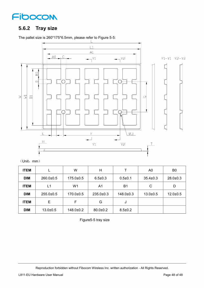
5.6.2 Tray size
The pallet size is 260*175*6.5mm, please refer to Figure 5-5:
(Unit:mm)
ITEM L W H T A0 B0
DIM 260.0±0.5 175.0±0.5 6.5±0.3 0.5±0.1 35.4±0.3 28.0±0.3
ITEM L1 W1 A1 B1 C D
DIM 255.0±0.5 170.0±0.5 235.0±0.3 148.0±0.3 13.0±0.5 12.0±0.5
ITEM E F G J
DIM 13.0±0.5 148.0±0.2 80.0±0.2 8.5±0.2
Figure5-5 tray size