Embed Size (px)
Citation preview

APPLICATION NOTE
AN255/1288
A DESIGNER’S GUIDE TO THE L200 VOLTAGE REGULATOR
Delivering 2 A at a voltage variable from 2.85 V to 36 V, the L200 voltage regulator is a versatile device thatsimplifies the design of linear supplies. This design guide describes the operation of the device and its ap-plications.
The introduction of integrated regulator circuits hasgreatly simplified the work involved in designingsupplies. Regulation and protection circuits requiredfor the supply, previously realized using discretecomponents, are now integrated in a single chip.This had led to significant cost and space saving aswell as increased reliability. Today the designer hasa wide range of fixed and adjustable, positive andnegative series regulators to choose from as well asan increasing number of switching regulators.
The L200 is a positive variable voltage regulatorwhich includes a current limiter and supplies up to2 A at 2.85 to 36 V.
The output voltage is fixed with two resistors or, if acontinuously variable output voltage is required,with one fixed and one variable resistor.
The maximum output current is fixed with a lowvalue resistor. The device has all the characteristicscommon to normal fixed regulators and these aredescribed in the datasheet. The L200 is particularlysuitable for applications requiring output voltagevariation or when a voltage not provided by the stan-dard regulators is required or when a special limitmust be placed on the output current.
The L200 is available in two packages :
Pentawatt - Offers easy assembly and good reliabil-ity. The guaranteed thermal resistance (Rth j-case) is3 °C/W (typically 2 °C/W) while if the device is usedwithout heatsink we can consider a guaranteedjunction-ambient thermal resistance of 50 °C/W.
TO-3 - For professional and military use or wheregood hermeticity is required.
The guaranteed junction-case thermal resistance is4 °C/W, while the junction-ambient thermal resis-tance is 35 °C/W.
The junction-case thermal resistance of this pack-age, which is greater than that of the Pentawatt, is
partly compensated by the lower contact resis-tancewith the heatsink, especially when an electrical in-sulator is used.
CIRCUIT OPERATION
As can be seen from the block diagram (fig. 1) thevoltage regulation loop is almost identical to that offixed regulators. The only difference is that the nega-tive feedback network is external, so it can be varied(fig. 3). The output is linked to the reference by :
Vout = Vref
( 1 +R2
) (1)R1
Considering Vout as the output of an operational am-plifier with gain equal to Gv = 1 + R2/R1 and inputsignal equal to Vref, variability of the output voltagecan be obtained by varying R1 or R2 (or both). It’sbest to vary R1 because in this way the current inresistors R1 and R2 remains constant (this currentis in fact given by Vref/R1).
Equation (1) can also be found in another way whichis more useful in order to understand the descrip-tions of the applications discussed.
Vout = R1 i1 + R2 i2and since in practice i1 » i4 (i4 has a typical value of10 µA) we can say that
Vout + R1 i1 + R2 i1 with i1 =Vref
R1
Therefore
Vout =R2
Vref + Vref = Vref ( 1 +R2
)R1 R1
In other words R1 fixes the value of the current cir-culating in R2 so R2 is determined.
1/21

Figure 1 : Block Diagram.
Figure 2 : Schematic Diagram.
APPLICATION NOTE
2/21

Figure 3.
OVERLOAD PROTECTION
The device has an overload protection circuit whichlimits the current available.
Referring to fig. 2, R24 operates as a current sensor.When at the terminals of R24 there is a voltage dropsufficient to make Q20 conduct, Q19 begins to drawcurrent from the base of the power transistor (dar-lington formed by Q22 and Q23) and the output cur-rent is limited. The limit depends on the currentwhich Q21 injects into the base of Q20. This currentdepends on the drop-out and the temperature whichexplains the trend of the curves in fig. 4.
Figure 4.
THERMAL PROTECTION
The junction temperature of the device may reachdestructive levels during a short circuit at the outputor due to an abnormal increase in the ambient tem-perature. To avoid having to use heatsinks whichare costly and bulky, a thermal protection circuit hasbeen introduced to limit the output current so that thedissipated power does not bring the junction tem-perature above the values allowed. The operation ofthis circuit can be summarized as follows.
In Q17 there is a constant current equal to :
Vref – VBE17 (Vref = 2.75 V typ)R17 + R16
The base of Q18 is therefore biased at :
VBE18 =Vref – VBE17 • R16 ≅ 350 mVR16 + R17
Therefore at Tj = 25 °C Q18 is off (since 600 mV isneeded for it to start conducting). Since the VBE ofa silicon transistor decreases by about 2 mV/°C,Q18 starts conducting at the junction temperature :
Tj =600 – 350
+ 25 = 150 °C2
CURRENT LIMITATION
The innovative feature of this device is the possibilityof acting on the current regulation loop, i.e. of limitingthe maximum current that can be supplied to the de-sired value by using a simple resistor (R3 in fig. 2).Obviously if R3 = 0 the maximum output current is
APPLICATION NOTE
3/21
also the maximum current that the device can sup-ply because of its internal limitation.
The current loop consists of a comparator circuitwith fixed threshold whose value is Vsc. This com-parator intervenes when Io . R3 = Vsc, hence
IO =VSC (VSC is the voltage between pin 5 R3
and 2 with typical value of 0.45 V).
Special attention has been given to the comparatorcircuit in order to ensure that the device behaves asa current generator with high output impedance.
TYPICAL APPLICATIONS
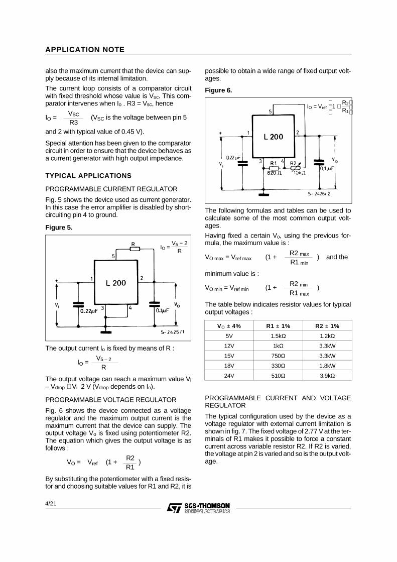
PROGRAMMABLE CURRENT REGULATOR
Fig. 5 shows the device used as current generator.In this case the error amplifier is disabled by short-circuiting pin 4 to ground.
Figure 5.
The output current Io is fixed by means of R :
IO = V5 – 2
R
The output voltage can reach a maximum value Vi– Vdrop ≅ Vi 2 V (Vdrop depends on Io).
PROGRAMMABLE VOLTAGE REGULATOR
Fig. 6 shows the device connected as a voltageregulator and the maximum output current is themaximum current that the device can supply. Theoutput voltage Vo is fixed using potentiometer R2.The equation which gives the output voltage is asfollows :
VO = Vref (1 +R2
)R1
By substituting the potentiometer with a fixed resis-tor and choosing suitable values for R1 and R2, it is
possible to obtain a wide range of fixed output volt-ages.
Figure 6.
The following formulas and tables can be used tocalculate some of the most common output volt-ages.
Having fixed a certain Vo, using the previous for-mula, the maximum value is :
VO max = Vref max (1 +R2 max ) and theR1 min
minimum value is :
VO min = Vref min (1 + R2 min )R1 max
The table below indicates resistor values for typicaloutput voltages :
VO ± 4% R1 ± 1% R2 ± 1%
5V 1.5kΩ 1.2kΩ
12V 1kΩ 3.3kW
15V 750Ω 3.3kW
18V 330Ω 1.8kW
24V 510Ω 3.9kΩ
PROGRAMMABLE CURRENT AND VOLTAGEREGULATOR
The typical configuration used by the device as avoltage regulator with external current limitation isshown in fig. 7. The fixed voltage of 2.77 V at the ter-minals of R1 makes it possible to force a constantcurrent across variable resistor R2. If R2 is varied,the voltage at pin 2 is varied and so is the output volt-age.
IO = Vref 1 +
R2
R1
IO = V5 − 2
R
APPLICATION NOTE
4/21

The output voltage is given by :
VO = Vref • (1 + R2 ), with Vref = 2.77 V typR1
and the maximum output current is given by :
IO max =V5–2 with V5–2 = 0.45 V typ.R3
To maintain a sufficient current for good regulationthe value of R1 should be kept low. When there isno load, the output current is Vref/R1. Suitable val-ues of R1 are between 500 Ω and 1.5 kΩ. If the loadis always present the maximum value for R1 is lim-ited by the current value (10 µA) at the input of theerror amplifier (pin 4).
Figure 7.
DIGITALLY SELECTED REGULATOR WITH IN-HIBIT
The output voltage of the device can be regulateddigitally as shown in fig. 8. The output voltage de-pends on the divider formed by R5 and a combina-tion of R1, R2, R3 and P2. The device can beswitched off with a transistor.
When the inhibit transistor is saturated, pin 2 isbrought to ground potential and the output voltagedoes not exceed 0.45 V.
REDUCING POWER DISSIPATION WITH DROP-PING RESISTOR
If may sometimes be advisable to reduce the powerdissipated by the device. A simple and economicmethod of doing this is to use a resistor connectedin series to the input as shown in fig. 9. The input-output differential voltage on the device is thus re-duced.
The formula for calculating R is as follows :
R =Vi min – (VO + Vdrop)
IO
Where Vdrop is the minimum differential voltage be-tween the input and the output of the device at cur-rent Io. Vin min is the minimum voltage. Vo is theoutput voltage and Io the output current.
With constant load, resistor R can be connected be-tween pins 1 and 2 of the IC instead of in series withthe input (fig. 10). In this way, part of the load currentflows through the device and part through the resis-tor. This configuration can be used when the mini-mum current by the load is :
IO min =Vdrop (instant by instant)
R
Figure 8.
Figure 9.IO = Vref 1 +
R2
R1
IO(max.) = V5 − 2
R
APPLICATION NOTE
5/21

Figure 10.
SOFT START
When a slow rise time of the output voltage is re-quired, the configuration in fig. 11 can be used. Therise time can be found using the following formula :
ton =CV o R
0.45
At switch on capacitor C is discharged and it keepsthe voltage at pin 2 low ; or rather, since a voltageof more than 0.45 V cannot be generated betweenpins 5 and 2, the Vo follows the voltage at pin 2 atless than 0.45 V.
Figure 11.
Capacitor C is charged by the constant current ic.
ic =Vsc
R
Therefore the output reaches its nominal value afterthe time ton :
VO – Vsc =IC • ton
C
ton = C • VO – 0.45 • R ≅ CVOR0.45 0.45
LIGHT CONTROLLER
Fig. 12 shows a circuit in which the output voltageis controlled by the brightness of the surrounding en-vironment. Regulation is by means of a photo resis-tor in parallel with R1. In this case, the outputvol-tage increases as the brightness increases. Theopposite effect, i.e. dimming the light as the ambientlight increases, can be obtained by connecting thephotoresistor in parallel with R2.
Figure 12.
LIGHT DIMMER FOR CAR DISPLAY
Although digital displays in cars are often more aes-thetically pleasing and frequently more easily readthey do have a problem. Under varying ambient lightconditions they are either lost in the background oralternatively appear so bright as to distract thedriver. With the system proposed here, this problemis overcome by automatically adjusting the displaybrightness during daylight conditions and by givingthe driver control over the brightness during duskand darkness conditions.
The circuit is shown in fig. 13. The primary supply isshown taken straight from the car battery howeverit is worth noting that in a car there is always the riskof dump voltages up to 120 V and it is recommendedthat some form of protection is included against this.
Under daylight conditions i.e. with sidelights off andT1 not conducting the output of the device is deter-mined by the values of R1, R2 and the photoresistor(PTR). The output voltage is given by
Vout = Vref (1 +R2
)PTR//R1
If the ambient light intensity is high, the resistanceof the photoresistor will be low and therefore Vout willbe high. As the light decreases, so Vout decreasesdimming the display to a suitable level.
APPLICATION NOTE
6/21

Figure 13.
In dusk conditions, when the sidelights are switchedon, T1 starts to conduct with its conduction set by thepotentiometer wiper at its uppermost position thesidelights are at their brightest and current throughT1 would be a minimum. With the wiper at its lowestposition obviously the opposite conditions apply.
The current through T1 is felt at the summing nodeA along with the currents through R2 and the parallelnetwork R1, PTR. Since Vref is constant the currentflowing through R1, PTR must also be constant.Therefore any change in the current through T1causes an equal and opposite change in the currentthrough R2. Therefore as IT1 increases, Vout de-creases i.e. as the brightness of the side-lights is in-creased or decreased so is the brightness of thedisplay.
The values of R2 and PTR should be selected togive the desired minimum and maximum brightnesslevels desired under both automatic and manualconditions although the minimum brightness undermanual conditions can also be set by the maximumcurrent flowing through T1 and, in any case, thisshould not exceed the maximum current through R2under automatic operation.
The circuit shown with a small modification can alsobe used for dimmers other than in a car. Fig. 15shows the modification needed. The zener diodeshould have a VF ≥ 2.5 V at I = 10 µA.
HIGHER INPUT OR OUTPUT VOLTAGES
Certain applications may require higher input or out-put voltages than the device can produce. The prob-lem can be solved by bringing the regulator back into
Figure 14.
Figure 15.
APPLICATION NOTE
7/21

the normal operating units with the help of externalcomponents.
When there are high input voltages, the excess vol-tage must be absorbed with a transistor. Figs. 16and 17 show the two circuits :
Figure 16.
Figure 17.
The designer must take into account the dissipatedpower and the SOA of the preregulation transistor.For example, using the BDX53, the maximum inputvoltage can reach 56 V (fig. 16). In these conditionswe have 20 V of VCEon the transistor and with a loadcurrent of 2 A the operation point remains inside theSOA. The preregulation used in fig. 16 reduces theripple at the input of the device, making it possibleto obtain an output voltage with negligible ripple.
If high output voltages are also required, a secondzener, VZ, is used to refer the ground pin of an IC toa potential other than zero ; diode D1 provides out-put shortcircuit protection (fig. 18).
Figure 18.
POSITIVE AND NEGATIVE VOLTAGE REGULA-TORS
The circuit in fig. 19 provides positive and negativebalanced, stabilized voltages simultaneously. TheL200 regulator supplies the positive voltage whilethe negative is obtained using an operational ampli-fier connected as follower with output currentbooster.
Tracking of the positive voltage is achieved by put-ting the non-inverting input to ground and using theinverting input to measure the feedback voltagecoming from divider R1-R2.
The system is balanced when the inputs of the op-erational amplifier are at the same voltage, or, sinceone input is at fixed ground potential, when the vol-tage of the intermediate point of the divider foes to0 Volts. This is only possible if the negative voltage,on command of the op-amp, goes to a value whichwill make a current equal to that in R1 flows in R2.The ratio which expresses the negative output vol-tage is :
V– = V+ • R2(If R2 = R1, we’ll get V– = V+)
R1
APPLICATION NOTE
8/21

Figure 19. Since the maximum supply voltage of the op ampused is ± 22 V, when pin 7 is connected to point Boutput voltages up to about 18 V can be obtained.If on the other hand pin 7 is connected to point A,much higher output voltages, up to about 30 V, beobtained since in this case the input voltage can riseto 34 V.
Fig. 20 shows a diagram is which the L165 powerop amp is used to produce the negative voltage. Inthis case (as in fig. 19) the output voltage is limitedby the absolute maximum rating of the supply vol-tage of the L165 which is ± 18 V. Therefore to get ahigher Vout we must use a zener to keep the devicesupply within the safety limits.
If we have a transformer with two separate secon-daries, the diagram of fig. 21 can be used to obtainindependent positive and negative voltages. Thetwo output diodes, D1 and D2, protect the devicesfrom shortcircuits between the positive and negativeoutputs.
Figure 20.
A : for ± 18 V ≤ Vi ≤ 32 VNote : Vz must be chosen in order to verify 2 Vi – Vz = 36 VB : for Vi ≤ ± 18 V
A : Vi(max) ≤ ± 34 V 3 < VO < 30B : Vi(max) ≤ ± 22 V 3 < VO < 18
APPLICATION NOTE
9/21

Figure 21. COMPENSATION OF VOLTAGE DROP ALONGTHE WIRES
The diagram in fig. 22 is particularly suitable whena load situated far from the output of the regulatorhas to be supplied and when we want to avoid theuse of two sensing wires. In fact, it is possible tocompensate the voltage drop on the line caused bythe load current (see the two curves in fig. 23 and24). RK transforms the load current IL into a propor-tional voltage in series to the reference of the L200.RK IL is then amplified by the factor
R2 + R1R1
With the values of RZ, R2 and R1 known, we get :
RK = RZR1
R1 + R2
RZ, R1 and R2 are assumed to be constant.
If RK is higher than 10 Ω , the output voltage shouldbe calculated as follows :
VO = Id RK + VrefR2 + R1
R1
Figure 22.
APPLICATION NOTE
10/21

Figure 23. Figure 24.
MOTOR SPEED CONTROL
Fig. 25 shows how to use the device for the speedcontrol of permanent magnet motors. The desiredspeed, proportional to the voltage at the terminal ofthe motor, is obtained by means of R1 and R2.
VM = Vref (1 + R2 )R1
To obtain better compensation of the internal motorresistance, which is essential for good regulation,the following equation is used :
R3 ≤ R1 • RM R2
This equation works with infinite R4. If R4 is finite,the motor speed can be increased without alteringthe ratio R2/R1 and R3. Since R4 has a constantvoltage (Vref) at its terminals, which does not vary asR4 varies, this voltage acts on R2 as a constant cur-rent source variable with R4. The voltage drop on R2thus increases, and the increase is felt by the volt-age at the terminals of the motor. The voltage in-crease at the motor terminals is :
VM =Vref • R2
R4 + R3
A circuit for a 30 W motor with RM = 4 Ω, R1 = 1 kΩ,R2 = 4.3 kΩ, R4 = 22 kΩ and R3 = 0.82 Ω has beenrealized.
POWER AMPLITUDE MODULATOR
In the configuration of fig. 26 the L200 is used tosend a signal onto a supply line. Since the input sig-nal Vi is DC decoupled, the Vo is defined by :
VO = Vref (1 +R2
)R1
Figure 25.
The amplified signal Vi whose value is :
GV = –R2R3
is added to this component. By ignoring the currententering pin 4, we must impose i1 = i2 + i3 (1) andsince the voltage between pin 4 and ground remainsfixed (Vref) as long as the device is not in saturation,i1 = 0 and equation (1) becomes :
i2 = – i3 with i3 =Vi (for Xc « R3) ThereforeR3
Vo = R2 i2 = –Vi • R2R3
An application is shown in fig. 27. If the DC level isto be varied but not the AC gain, R1 should be re-placed by a potentiometer.
APPLICATION NOTE
11/21

Figure 26.
Figure 27.
HIGH CURRENT REGULATORS
To get a higher current than can be supplied by a sin-gle device one or more external power transistorsmust be introduced. The problem is then to extendall the device’s protection circuits (short-circuit pro-tection, limitation of Tj of external power devices andoverload protection) to the external transistors. Con-stant current or foldback current limitation thereforebecomes necessary.
When the regulator is expected to withstand a per-manent shortcircuit, constant current limitation be-comes more and more difficult to guarantee as thenominal Vo increases. This is because of the in-crease in VCE at the terminals of the transistor, whichleads to an increase in the dissipated power. Theheatsink has to be calculated in the heaviest workingconditions, and therefore in shortcircuit. This in-creases weight, volume and cost of the heatsink andincrease of the ambient temperature (because ofhigh power dissipation). Besides heatsink, power
transistors must be dimensioned for the short-cir-cuit.
This type, of limitation is suited, for example, withhighly capacitive loads. Efficiency is increased if pre-regulation is used on the input voltage to maintain aconstant drop-out on the power element for all Vout,even in shortcircuit. Foldback limitation, on the otherhand, allows lighter shortcircuit operating conditionsthan the previous case. The type of load is impor-tant.
If the load is highly capacitive, it is not possible tohave a high ratio between Imax and Isc because atswitch-on, with load inserted, the output may notreach its nominal value.
Other protection against input shortcircuit, mainsfailure, overvoltages and output reverse bias can berealized using two diodes, D1 and D2, inserted asindicated in fig. 28.
APPLICATION NOTE
12/21

Figure 28.
USE OF A PNP TRANSISTOR
Fig. 29 shows the diagram of a high current supplyusing the current limitation of the L200. The outputcurrent is calculated using the following formula :
Io = VSC ≅ 0.45 V = 4.5 ARSC 0.1 Ω
Constant current limitation is used ; so, in outputshortcircuit conditions, the transistor dissipates apower equal to :
PD = Vi • Io = Vi •VSC
RSC
The operating point of the transistor should be keptwell within the SOA ; with RSC = 0.1 Ω, Vi must notexceed 20 V. Part of the Io crosses the transistor andpart crosses the regulator.
Figure 29.
The latter is given by : IREG = IB +VBE
R
where IB is the base current of the transistor (–100 mA at IC = 4 A) and VBE is the base-emitter volt-age (– 1 V at IC = 4 A) ; with R = 2.5 Ω, IREG ≅ 500mA.
USE OF AN NPN POWER TRANSISTOR
Fig. 30 shows the same application as described infigure 29, using an NPN power transistor instead ofa PNP. In this case an external signal transistor mustbe used to limit the current. Therefore :
Io =VBE Q1
RSC
As regards the output shortcircuit, see par. 1.5.
Figure 30.
APPLICATION NOTE
13/21

12V - 4A POWER SUPPLY
The diagram in fig. 31 shows a supply using theL200 and the BD705. The 1 kΩ potentiometer, PT1,together with the 3.3 k resistor are used for fine regu-lation of the output voltage.
Current limitation is of the type shown in fig. 32.Trimmer PT2 acts on strech AB of characteristic.With the values indicated (PT2 = 1 kΩ, PT3 = 470 Ω,R = 3 kΩ), currents from 3 to 4 A can be limited. Thefield of variation can be increased by increasing thevalue of RSC or by connecting one terminal of PT tothe base of the power transistor, which, however,provides less stable limitation. If section AB ismoved, section BC will also be moved.
The slope of BC can be varied using PT3. The vol-tage level at point B is fixed by the voltage of thezener diode. The capacitor in parallel to the zenerensures correct switch-on with full load. The BD705should always be used well within its safe operatingarea. If this is not possible two or more BD705sshould be used, connected in parallel (fig. 33).
Further protection for the external power transistorcan be provided as shown in fig. 34. The PTC resis-tor, whose temperature intervention point must pre-vent the Tj of the power transistor from reaching itsmaximum value, should be fixed to the dissipatornear the power transistor. Dimensioning of RA andRB depends on the PTC used.
Figure 31.
APPLICATION NOTE
14/21

Figure 32. Figure 33.
Figure 34. VOLTAGE REGULATOR FROM 0V TO 16V - 4.5A
Fig. 35 shows an application for a high current sup-ply with output voltage adjustable from 0 V to 16 V,realized with two L200 regulators and an externalpower transistor. With the values indicated, the cur-rent can be regulated from 2 A to 4.5 A by potenti-ometer PT2. PT1, on the other hand, is used for con-stant current or foldback current limitation. The inte-grated circuit IC2, which does not require a heatsinkand has excellent temperature stability, is used toobtain the 0 V output. It is connected so as to lowerpin 3 of IC1 until pin 4 reaches 0 V. Q1 and Q2 en-sure correct operation of the supply at switch-on andswitch-off.
APPLICATION NOTE
15/21

Figure 35.
POWER SUPPLY WITH Vo = 2.8 TO 18 V, Io = 0 TO2.5 A
The diagram in fig. 36 shows a supply with outputvoltage variable from 2.8 V to 18 V and constant cur-rent limitation from 0 A to 2.5 A. The output currentcan be regulated over a wide range by means of theop. amp. and signal transistor TR2. The op. amp.and the transistor are connected in the voltage-cur-rent converter configuration. The voltage is taken atthe terminals of R3 and converted into current byPT2.
Io is fixed as follows :
R4 Io = I1 (*) (**) Isc =VSC
PT2 R2
When I1 = Isc, the regulator starts to operate as a cur-rent generator. By making (*) equal to (**) we get :R4 Io
=VSC
; Therefore Io =VSC
• PT2 PT2 R2 R2 • R4
Diodes D1 and D2 keep transistor TR2 in linear con-dition in the case of small output currents. If it is notnecessary to limit the current to zero, one of the di-odes can be eliminated : the second diode couldalso be eliminated if TR1 were a darlington insteadof a transistor.
The op. amp. must have inputs compatible withground in order to guarantee current limitation evenin shortcircuit. With a negative voltage available,even of only &a few volts, current limitation is sim-plified.
APPLICATION NOTE
16/21

Figure 36.
LAYOUT CONSIDERATIONS
The performance of a regulator depends to a greatextent on the case with which the printed circuit isproduced. There must be no impulsive currents (likethe one in the electrolytic filter capacitor at the inputof the regulator) between the ground pin of the de-vice (pin 3) and the negative output terminal be-cause these would increase the output ripple. Caremust also be taken when inserting the resistor con-nected between pin 4 and pin 3 of the device.
The track connecting pin 3 to a terminal of this re-sistor should be very short and must not be crossed
by the load current (which, since it is generally vari-able, would give rise to a voltage drop on this stretchof track, altering the value of Vref and therefore of Vo.
When the load is not in the immediate proximity ofthe regulator output "+ sense" and " – sense" termi-nals should be used (see fig. 37). By connecting the"+ sense" and "– sense" terminals directly at thecharge terminals the voltage drop on the connectioncable between supply and load are compensated.Fig. 37 shows how to connect supply and load usingthe sensing clamps terminals.
Figure 37.
APPLICATION NOTE
17/21

Figure 38.
HEATSINK DIMENSIONING
The heatsink dissipates the heat produced by thedevice to prevent the internal temperature fromreaching value which could be dangerous for deviceoperation and reliability.
Integrated circuits in plastic package must never ex-ceed 150 °C even in the worst conditions. This limithas been set because the encapsulating resin hasproblems of vitrification if subjected to temperaturesof more than 150 °C for long periods or of more than170 °C for short periods (24 h). In any case the tem-perature accelerates the ageing process and there-fore influences the device life ; an increase of 10 °Ccan halve the device life. A well designed heatsinkshould keep the junction temperature between90 °C and 110 °C. Fig. 39 shows the structure of apower device. As demonstrated in thermodynamics,a thermal circuit can be considered to be an electri-cal circuit where R1, 2 represent the thermal resis-tance of the single elements (expressed in C/W) ;
Figure 40.
Figure 39.
C1, 2 the thermal capacitance (expressed in °C/W) I the dissipated power V the temperature difference with respect to
the reference (ground)
This circuit can be simplified as follows :
Figure 41.
Where Ce is the thermal capacitance of the die plusthat of the tab.
Ch is the thermal capacitance of the heatsinkRjc is the junction case thermal resistanceRh is the heatsink thermal resistance
But since the aim of this section is not that of studingthe transistors, the circuit can be further reduced.
APPLICATION NOTE
18/21

Figure 42.
If we now consider the ground potential as ambienttemperature, we have :
Ti = Ta + (Rjc + Rh) PD (1)
Rth = Ti – Ta – RIC • Pd (1a)Pd
Tc = Ta + Rh • Pd (2)
For example, consider an application of the L200with the following characteristics :
Vin typ = 20 VVo = 14 V
typical conditionsIo typ = 1 ATa = 40 °C
Vin max = 22 VVo = 14 V
overload conditionsIo max = 1.2 ATa = 60 °C
Pd typ = (Vin – Vo) • Io = (2014) • 1 = 6 W
Pd max = (2214)•1.2 = 9.6 W
Imposing Tj = 90 °C of (1a) we get (from L200 char-acteristics we get Rjc = 3 °C/W).
Rh =90 – 40 – 3•6
= 5.3 °C/W6
Using the value thus obtained in (1), we get that thejunction temperature during the overload goes to thefollowing value :
Tj = 60 + (3 + 5.3) . 9.6 = 140 °C
If the overload occurs only rarely and for short peri-ods, dimensioning can be considered to be correct.Obviously during the shortcircuit, the dissipatedpower reaches must higher values (about 40 W forthe case considered) but in this case the thermalprotection intervenes to maintain the temperaturebelow the maximum values allowed.
Note 1 : If insulating materials are used between de-vice and heatsink, the thermal contact resistancemust be taken into account (0.5 to 1 °C/W, depend-ing on the type of insulant used) and the circuit in fig.43 becomes :
Figure 43.
Note 2 : In applications where one or more externaltransistors are used together with the L200, the dis-sipated power must be calculated for each compo-nent. The various junction temperatures can becalculated by solving the following circuit :
Figure 44.
This applies if the various dissipating elements arefairly near to one another with respect to theheatsink dimensions, otherwise the heatsink can nolonger be considered as a concentrated constantand the calculation becomes difficult.
This concept is better explained by the graph in fig.45 which shows the case (and therefore junction)temperature variation as a function of the distancebetween two dissipating elements with the sametype of dissipator and the same dissipated power.The graph in fig. 45 refers to the specific case of twoelements dissipating the same power, fixed on arectangular aluminium plate with a ratio of 3 bet-ween the two sides. The temperature jump will de-pend on the dissipated power and one the devicegeometry but we want to show that there exists anoptimal position between the two devices :
d =1 • side of the plate2
Fig. 46 shows the trend of the temperature as a func-tion of the distance between two dissipating ele-
APPLICATION NOTE
19/21

ments whose dissipated power is fairly different (ra-tio 1 to 4).
This graph may be useful in applications with theL200 + external transistor (in which the transistorgenerally dissipates more than the L200) where thetemperature of the L200 has to be kept as low aspossible and especially where the thermal protec-tion of the L200 is to be used to limit the transistor
temperature in the case of an overload or abnormalincrease in the ambient temperature. In other wordsthe distance between the two elements can be se-lected so that the power transistor reaches the Tj max(200 °C for a TO-3 transistor) when the L200reaches the thermal protection intervention tem-perature.
Figure 45.
Figure 46.
A : Position of the device with high power dissipation (10 W)B : Position of the device with low power dissipation (2.5 W)
APPLICATION NOTE
20/21

Information furnished is believed to be accurate and reliable. However, SGS-THOMSON Microelectronics assumes no responsibility for theconsequences of use of such information nor for any infringement of patents or other rights of third parties which may result from its use.No license is granted by implication or otherwise under any patent or patent rights of SGS-THOMSON Microelectronics. Specificationsmentioned in this publication are subject to change without notice. This publication supersedes and replaces all information previouslysupplied. SGS-THOMSON Microelectronics products are not authorized for use as critical components in life support devices or systemswithout express written approval of SGS-THOMSON Microelectronics.
© 1995 SGS-THOMSON Microelectronics - All Rights Reserved
SGS-THOMSON Microelectronics GROUP OF COMPANIES
Australia - Brazil - France - Germany - Hong Kong - Italy - Japan - Korea - Malaysia - Malta - Morocco - The Netherlands - Singapore -Spain - Sweden - Switzerland - Taiwan - Thaliand - United Kingdom - U.S.A.
APPLICATION NOTE
21/21