Embed Size (px)
Citation preview
L16: 6.111 Spring 2004 1Introductory Digital Systems Laboratory
L16: Power Dissipation in Digital SystemsL16: Power Dissipation in Digital Systems
L16: 6.111 Spring 2004 2Introductory Digital Systems Laboratory
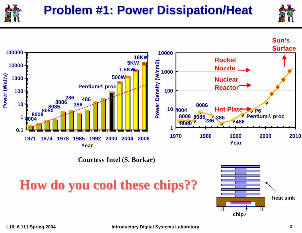
Problem #1: Power Dissipation/HeatProblem #1: Power Dissipation/Heat
5KW 18KW
1.5KW 500W
40048008
80808085
8086286
386486
Pentium® proc
0.1
1
10
100
1000
10000
100000
1971 1974 1978 1985 1992 2000 2004 2008Year
Pow
er (W
atts
)
400480088080
8085
8086
286 386486
Pentium® procP6
1
10
100
1000
10000
1970 1980 1990 2000 2010Year
Pow
er D
ensi
ty (W
/cm
2)
Hot Plate
NuclearReactor
RocketNozzle
How do you cool these chips??How do you cool these chips??
chip
heat sink
Sun’sSurface
Courtesy Intel (S. Borkar)
L16: 6.111 Spring 2004 3Introductory Digital Systems Laboratory
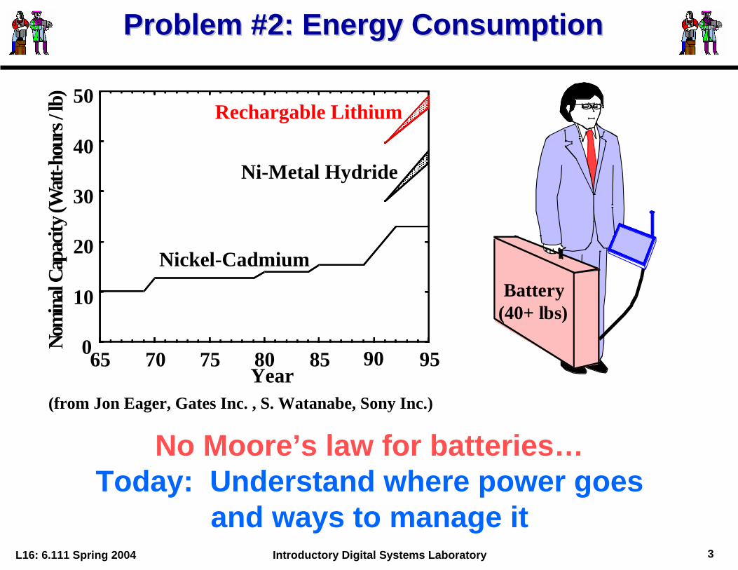
Problem #2: Energy ConsumptionProblem #2: Energy Consumption
(40+ lbs)Battery
Year
Nom
inal
Capa
city(
Wat
t-hou
rs/lb
)
Nickel-Cadmium
Ni-Metal Hydride
65 70 75 80 85 90 95 0
10
20
30
40
50 Rechargable Lithium
(from Jon Eager, Gates Inc. , S. Watanabe, Sony Inc.)
No Moore’s law for batteries…Today: Understand where power goes
and ways to manage it
L16: 6.111 Spring 2004 4Introductory Digital Systems Laboratory
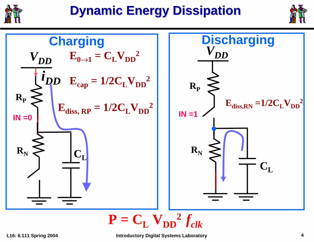
Dynamic Energy DissipationDynamic Energy Dissipation
VDD
CL
E0→1 = CLVDD2
Ecap = 1/2CLVDD2iDD
Ediss, RP = 1/2CLVDD2
VDD
CL
IN =1Ediss,RN =1/2CLVDD
2
Charging Discharging
IN =0
P = CL VDD2 fclk
RN
RP
RN
RP
L16: 6.111 Spring 2004 5Introductory Digital Systems Laboratory
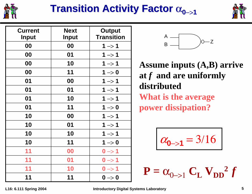
TransitionTransition Activity Factor Activity Factor αα00−−>>11
Output Transition
Next Input
Current Input
0 −> 011110 −> 110110 −> 101110 −> 100111 −> 011101 −> 110101 −> 101101 −> 100101 −> 011011 −> 110011 −> 101011 −> 100011 −> 011001 −> 110001 −> 101001 −> 10000
α0−>1 = 3/16
Assume inputs (A,B) arrive at f and are uniformly distributedWhat is the average power dissipation?
P = α0−>1 CL VDD2 f
ZAB

L16: 6.111 Spring 2004 6Introductory Digital Systems Laboratory
Junction (Silicon) TemperatureJunction (Silicon) Temperature
Simple Scenario
Tj-Ta= RθJA PD
Silicon
RθJA is the thermal resistance between silicon and Ambient
RθJAPD
Tj= Ta + RθJA PD
Make this as low as possible
Realistic Scenario
RθJCPD
RθCA = RθCS + RθSA
SinkCase
Silicon
TJ
TA
TJ
TC
TS
TATJ
TC
TS
TA
RθCS
RθSA
is minimized by facilitating heat transfer (bolt case to extended metal surface – heat sink)
L16: 6.111 Spring 2004 7Introductory Digital Systems Laboratory
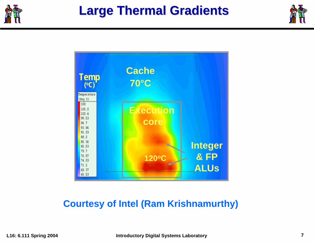
Large Thermal GradientsLarge Thermal Gradients
Execution core
120oC
Cache70°C
Integer & FP ALUs
Temp(oC)
Courtesy of Intel (Ram Krishnamurthy)
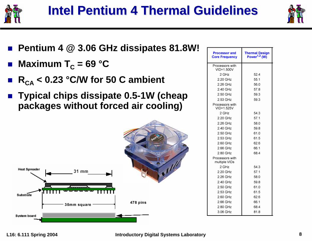
L16: 6.111 Spring 2004 8Introductory Digital Systems Laboratory
Intel Pentium 4 Thermal GuidelinesIntel Pentium 4 Thermal Guidelines
Pentium 4 @ 3.06 GHz dissipates 81.8W!Maximum TC = 69 °CRCA < 0.23 °C/W for 50 C ambientTypical chips dissipate 0.5-1W (cheap packages without forced air cooling)

L16: 6.111 Spring 2004 9Introductory Digital Systems Laboratory
Power Reduction StrategiesPower Reduction Strategies
Reduce Transition Activity or Switching EventsReduce Capacitance (e.g., keep wires short)Reduce Power Supply VoltageFrequency is typically fixed by the application, though this can be adjusted to control power
P = α0−>1 CL VDD2 f
Optimize at all levels of design hierarchyOptimize at all levels of design hierarchy
L16: 6.111 Spring 2004 10Introductory Digital Systems Laboratory
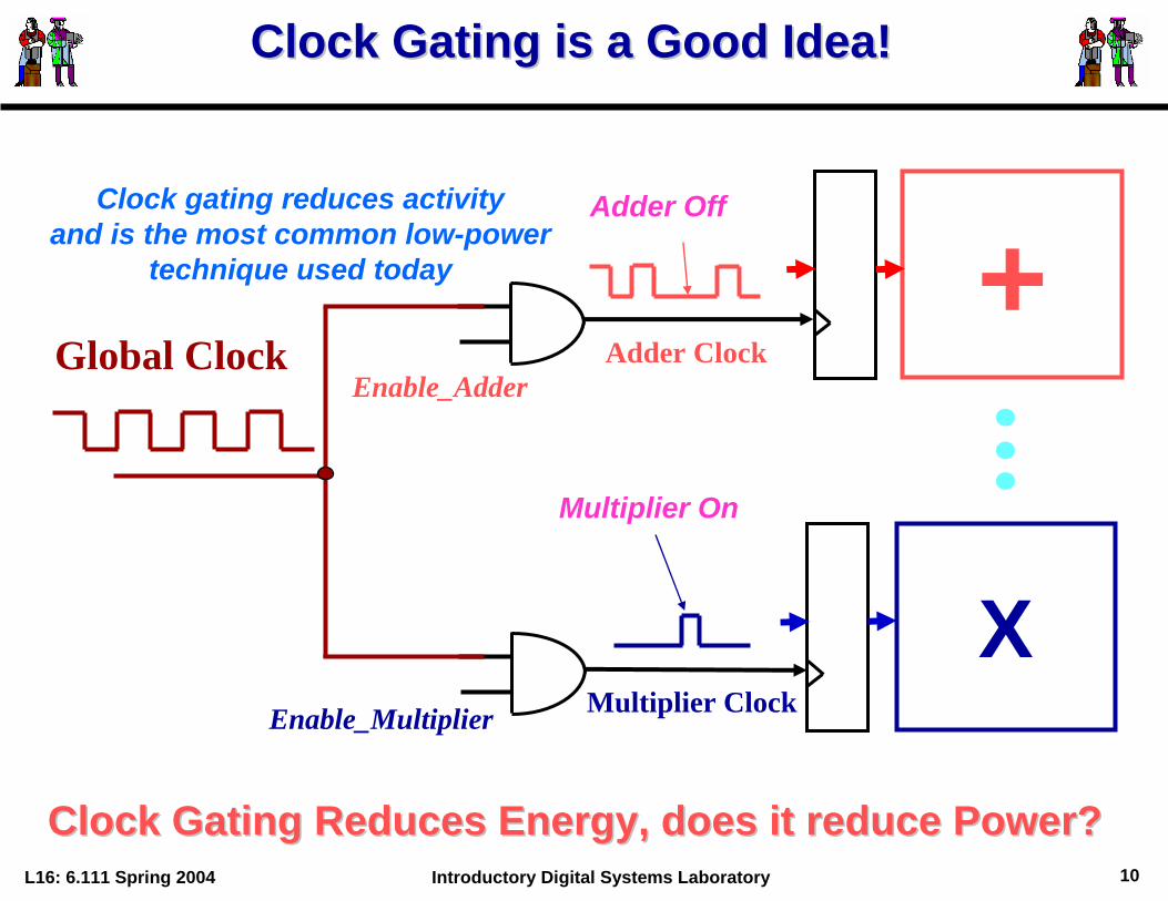
Clock Gating is a Good Idea!Clock Gating is a Good Idea!
+
X
Global Clock Adder Clock
Multiplier Clock
Adder Off
Enable_Adder
Enable_Multiplier
Multiplier On
Clock Gating Reduces Energy, does it reduce Power?Clock Gating Reduces Energy, does it reduce Power?
Clock gating reduces activityand is the most common low-power
technique used today
L16: 6.111 Spring 2004 11Introductory Digital Systems Laboratory
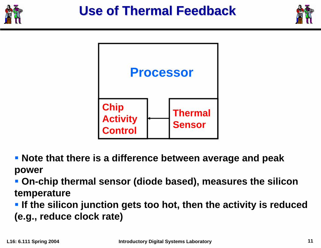
Use of Thermal FeedbackUse of Thermal Feedback
Processor
ThermalSensor
Note that there is a difference between average and peak power
On-chip thermal sensor (diode based), measures the silicon temperature
If the silicon junction gets too hot, then the activity is reduced (e.g., reduce clock rate)
ChipActivity Control

L16: 6.111 Spring 2004 12Introductory Digital Systems Laboratory
Power Supply Power Supply ParasiticsParasitics
Lboard Lpackage Rgrid
Switchingcurrents
Board decap
On-diedecap
Courtesy of Motorola(David Blaauw)
Courtesy of MotorolaCourtesy of Motorola(David Blaauw)(David Blaauw)
200MhzDesign

L16: 6.111 Spring 2004 13Introductory Digital Systems Laboratory
Power Supply Resonance!Power Supply Resonance!
L16: 6.111 Spring 2004 14Introductory Digital Systems Laboratory
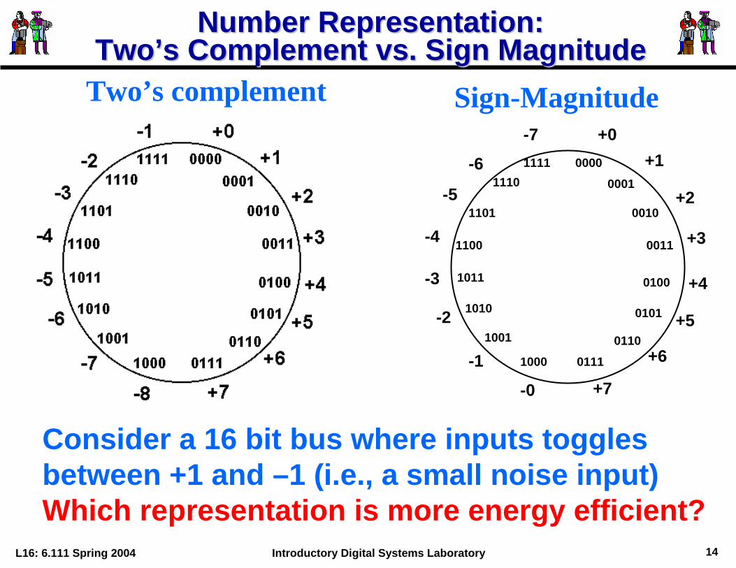
Number Representation:Number Representation:Two’s Complement vs. Sign MagnitudeTwo’s Complement vs. Sign Magnitude
Two’s complement
0000
0111
0011
1011
11111110
1101
1100
1010
1001
1000
0110
0101
0100
0010
0001
+0+1
+2
+3
+4
+5
+6
+7-0
-1
-2
-3
-4
-5
-6
-7
Sign-Magnitude
Consider a 16 bit bus where inputs togglesbetween +1 and –1 (i.e., a small noise input)Which representation is more energy efficient?
L16: 6.111 Spring 2004 15Introductory Digital Systems Laboratory
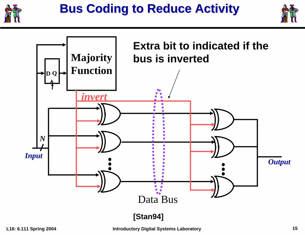
Bus Coding to Reduce ActivityBus Coding to Reduce Activity
MajorityFunction
invert
D Q
Input
Data Bus
N
Output
[Stan94]
Extra bit to indicated if thebus is inverted
L16: 6.111 Spring 2004 16Introductory Digital Systems Laboratory
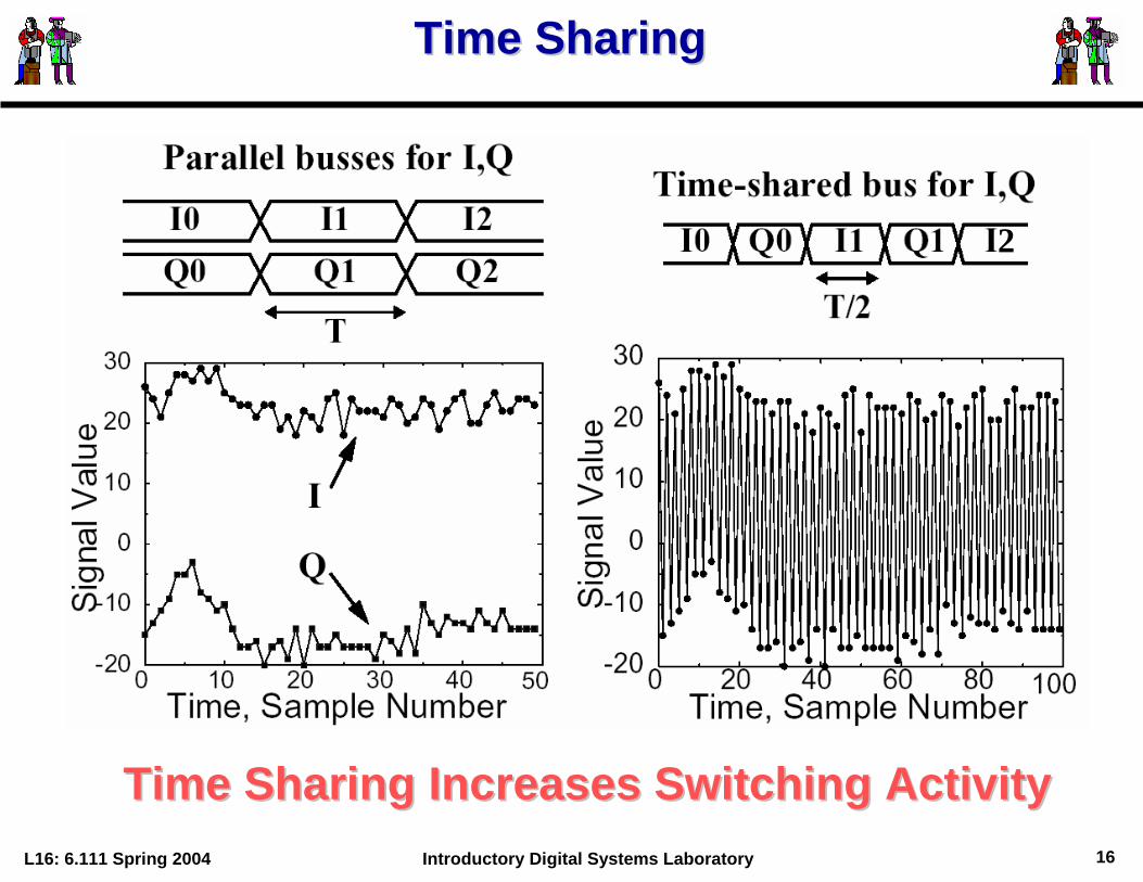
Time SharingTime Sharing
Time Sharing Increases Switching ActivityTime Sharing Increases Switching Activity
2

L16: 6.111 Spring 2004 17Introductory Digital Systems Laboratory
Not just a 6Not just a 6--1 Issue: “Cool” Software ???1 Issue: “Cool” Software ???
CPU
0111111100000000
0111111100000001
0111111100000010
0111111100000011
1000000000000000
1000000000000001
1000000000000010
1000000000000011
float a [256], b[256];float pi= 3.14;
for (i = 0; i < 255; i++) {a[i] = sin(pi * i /256);}for (i = 0; i < 255; i++) {b[i] = cos(pi * i /256);}
float a [256], b[256];float pi= 3.14;
for (i = 0; i < 255; i++) {a[i] = sin(pi * i /256);b[i] = cos(pi * i /256);
}
a[0]a[1]a[2]a[3]
b[0]b[1]b[2]b[3]
address
MEMORY address
16
512(8)+2+4+8+16+32+64+128+256= 4607 bit transitions
2(8)+2(2+4+8+16+32+64+128+256)= 1030 transitions
L16: 6.111 Spring 2004 18Introductory Digital Systems Laboratory
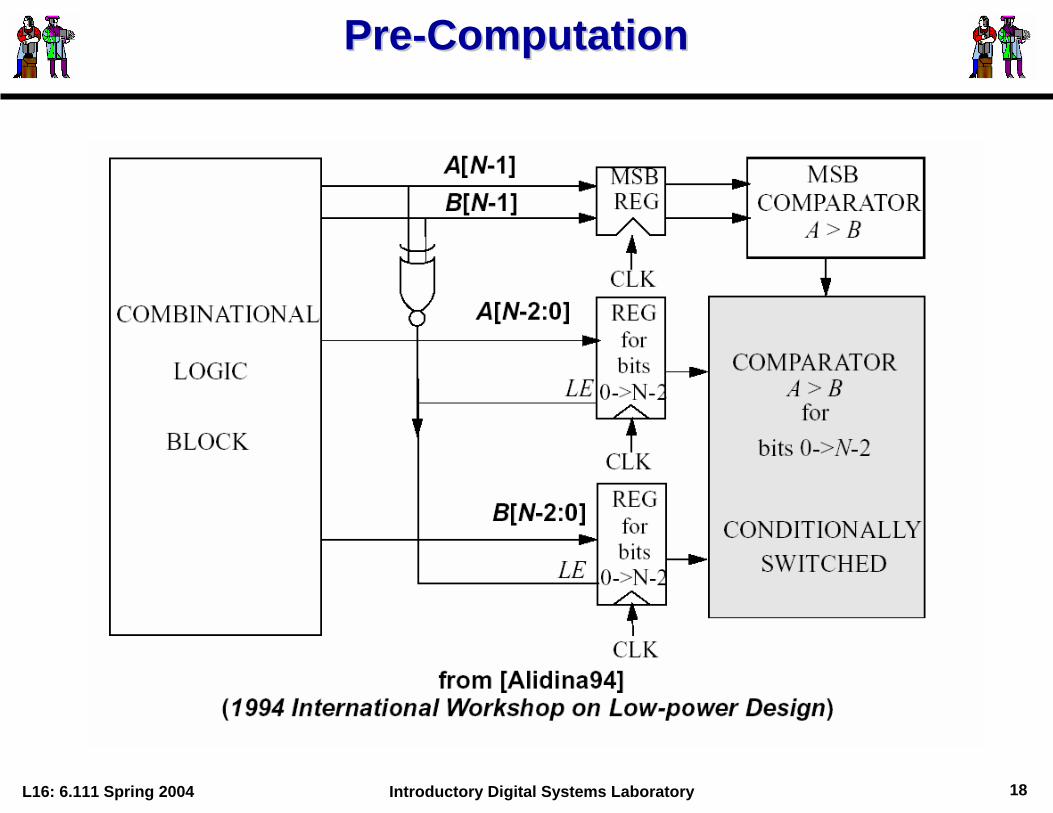
PrePre--ComputationComputation

L16: 6.111 Spring 2004 19Introductory Digital Systems Laboratory
GlitchingGlitching TransitionsTransitions
Balancing paths reduces glitching transitionsFor 4 inputs, 50% less transitions using a tree approachStructures such as multipliers have lot of glitching transitionsKeeping logic depths short (e.g., pipelining) reduces glitching
++
+
A B C D
(A+B) + (C+D)+
+
+
A B
C
D
(((A+B) + C)+D)
Chain Topology Tree Topology

L16: 6.111 Spring 2004 20Introductory Digital Systems Laboratory
Reduce Supply Voltage : But is it Free?Reduce Supply Voltage : But is it Free?
IN OUT
VDD
+
-CL
t =0+
2)(2 T
VDD
VK
−
VDD
VSG
S
D
DDV
DDTDD
DD
VVVV
TV
DDV
k
DDV
LC
Di
VL
CDelay
1)( 2
2)(2
2 ≈−
∝
−
⋅=
∆⋅=
VDD from 2V to 1V, energy ↓ by x4, delay ↑ x2
L16: 6.111 Spring 2004 21Introductory Digital Systems Laboratory
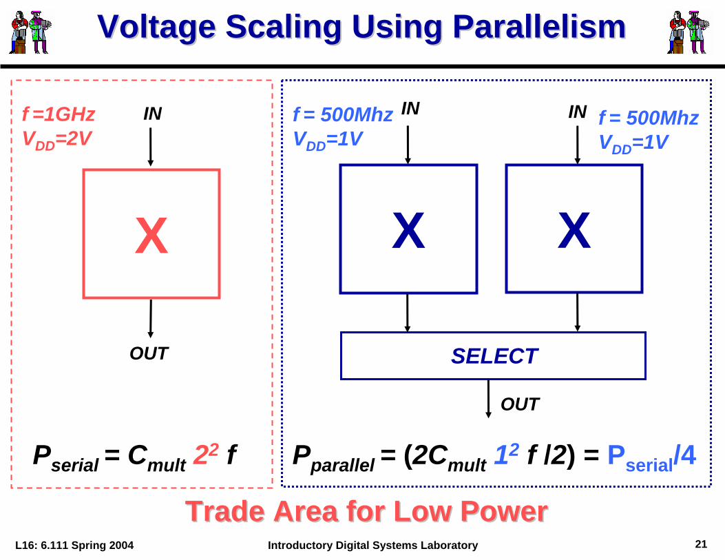
Voltage Scaling Using ParallelismVoltage Scaling Using Parallelism
OUT
IN
X
Pserial = Cmult 22 f Pparallel = (2Cmult 12 f /2) = Pserial/4
f =1GHzVDD=2V
X X
INf = 500MhzVDD=1V
f = 500MhzVDD=1V
IN
SELECT
Trade Area for Low PowerTrade Area for Low Power
OUT
L16: 6.111 Spring 2004 22Introductory Digital Systems Laboratory
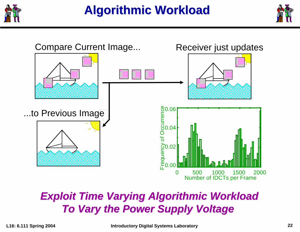
Algorithmic WorkloadAlgorithmic Workload
Receiver just updatesCompare Current Image...
...to Previous Image
Fre
quen
cyof
Occ
urre
nce
Number of IDCTs per Frame0 500 1000 1500 2000
0.00
0.02
0.04
0.06
Exploit Time Varying Algorithmic WorkloadExploit Time Varying Algorithmic WorkloadTo Vary the Power Supply Voltage To Vary the Power Supply Voltage

L16: 6.111 Spring 2004 23Introductory Digital Systems Laboratory
Dynamic Voltage ScalingDynamic Voltage Scaling
ACTIVE IDLE
EFIXED = ½ C VDD2
Fixed Power SupplyACTIVE
EVARIABLE = ½ C (VDD/2)2 = EFIXED / 4
Variable Power Supply
0.2 0.4 0.8 1.0
0.2
0.4
0.6
0.8
1.0
Normalized Workload
Nor
mal
ized
Ene
rgy
Fixed Supply
VariableSupply
00 0.6
[Gutnik97]
L16: 6.111 Spring 2004 24Introductory Digital Systems Laboratory
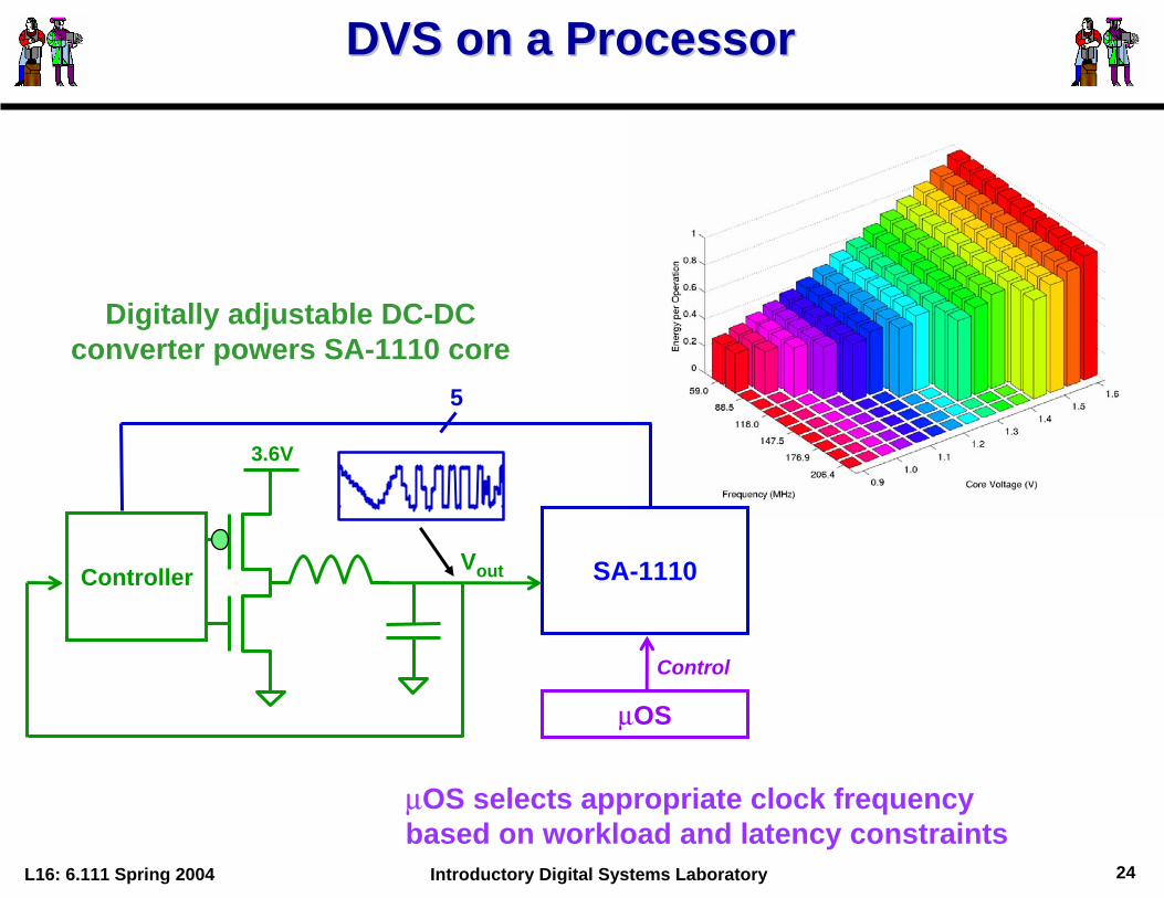
DVS on a ProcessorDVS on a Processor
Digitally adjustable DC-DC converter powers SA-1110 core
µOS selects appropriate clock frequency based on workload and latency constraints
SA-1110
Control
µOS
VoutController
3.6V
5
L16: 6.111 Spring 2004 25Introductory Digital Systems Laboratory
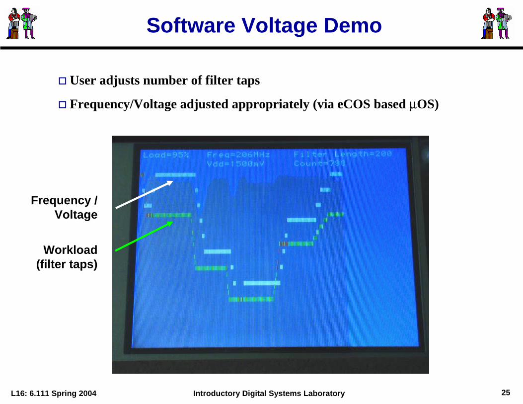
User adjusts number of filter taps
Frequency/Voltage adjusted appropriately (via eCOS based µOS)
Frequency /Voltage
Workload (filter taps)
Software Voltage Demo

L16: 6.111 Spring 2004 26Introductory Digital Systems Laboratory
Energy ScavengingEnergy Scavenging
Jose Mur Miranda/ Jeff Lang
Vibration-to-Electric Conversion
~ 10µW
MEMS Generator Power Harvesting Shoes
Joe Paradiso(Media Lab)
After 3-6 steps, it provides 3 mAfor 0.5 sec
~10mW