Embed Size (px)
Citation preview
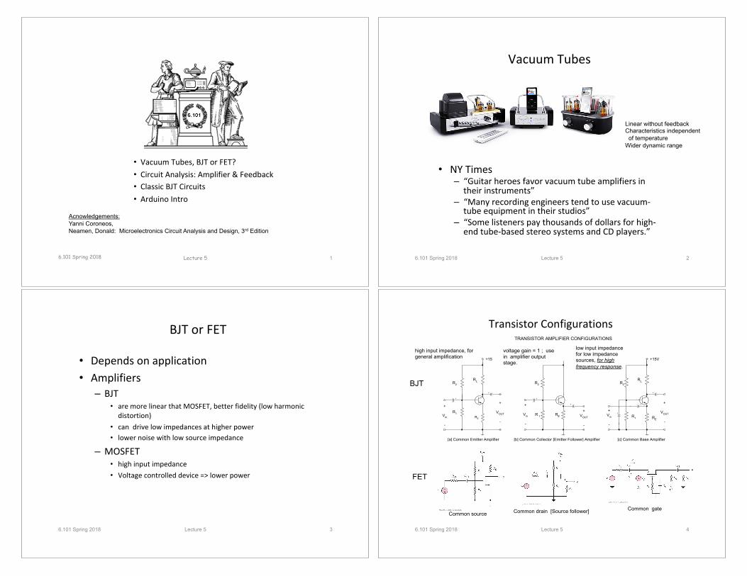
• VacuumTubes,BJTorFET?• CircuitAnalysis:Amplifier&Feedback• ClassicBJTCircuits• ArduinoIntro
6.101 Spring 2018 Lecture 5 1
Acnowledgements: Yanni Coroneos, Neamen, Donald: Microelectronics Circuit Analysis and Design, 3rd Edition
VacuumTubes
• NYTimes– “Guitarheroesfavorvacuumtubeamplifiersintheirinstruments”
– “Manyrecordingengineerstendtousevacuum-tubeequipmentintheirstudios”
– “Somelistenerspaythousandsofdollarsforhigh-endtube-basedstereosystemsandCDplayers.”
6.101 Spring 2018 Lecture 5 2
Linear without feedback Characteristics independent of temperature Wider dynamic range
BJTorFET
• Dependsonapplication• Amplifiers
– BJT• aremorelinearthatMOSFET,betterfidelity(lowharmonicdistortion)
• candrivelowimpedancesathigherpower• lowernoisewithlowsourceimpedance
– MOSFET• highinputimpedance• Voltagecontrolleddevice=>lowerpower
6.101 Spring 2018 Lecture 5 3
TransistorConfigurations
6.101 Spring 2018 Lecture 5 4
+15V
+
Vin
-
+
VOUT
-
RL
R1
+
+
R2
[a] Common Emitter Amplifier [b] Common Collector [Emitter Follower] Amplifier
RE RE
+15V
+Vin
-
+
VOUT
-
RL
R1
+
+
R2
+
[c] Common Base Amplifier
TRANSISTOR AMPLIFIER CONFIGURATIONS
R2
+15V
R 1
+
Vin
-
+VOUT
-
RE
+
+
high input impedance, for general amplification
voltage gain = 1 ; use in amplifier output stage.
low input impedance for low impedance sources, for high frequency response.
BJT
FET
Common source Common drain [Source follower] Common gate

MillerEffect*–CommonEmitter
6.101 Spring 2018 Lecture 3 5
)](1[ LCmM RRgCC += µ
* Agarwal & Lang Foundations of Analog & Digital Electronics Circuits p 861
InputImpedanceandFrequencyResponse
6.101 Spring 2018 6
RV1 V2C
Av =V2V1=
j XCR+ j XC
=
1jωC
R+ 1jωC
=1
jωRC +1
Av =1
sRC +1
High frequency cutoff fhi =1
2πRC
log f
AV (dB)
-3dB
fHI or f-3dB
slope = -6 dB / octaveslope = -20 dB / decade
0
log f
Degrees
-45o
fHI or f-3dB
0o
-90o
PHASE LAG
Lecture 2
log scale
LowFrequencyHybrid-πEquationChart
6.101 Spring 2018 Lecture 5 7
High gain, better high frequency response Low input resistance
Unity gain, low output resistance High input resist.
High gain applications Moderate input resistance High output resistance
CascodeAmplifer
• Twotransistoramplifer:commonemitter(CE)withacommonbase
• MillereffectavoidedbysettinggainofCEstagelow.
• CEstageprovideshighinputimpedance
• Commonbase(CB)providesgainwithoutMillereffect;baseisgrounded.
6.101 Spring 2018 Lecture 5 8
Miller effect
No Miller effect

Objectives
• PerformananalysisintothebehaviorofacomplicatedcircuitusingbasicpropertiesofBJT’s(npn,pnp)
• Calculategainofthesystem
• Discusscrossoverdistortionissuesinpush-pullamplifiers
• Understandfeedback
6.101 Spring 2018 Lecture 5 9
ThreeStage–PushPullAmplifier
6.101 Spring 2018 Lecture 5 10
6.101 Spring 2018 Lecture 5 11
ThreeStageAmplifer–BlockDiagram
Feedback
Q3-Q4PushPull
6.101 Spring 2018 Lecture 5 12
• Q3:EmitterFollower(positvecycle)
• Q4:EmitterFollower(negativecycle)
• Overallgain~1
• Q3&Q4Vbearealwaysonediodedrop
• Crossoverdistortion
aboutzerocrossing

CrossoverDistortion
6.101 Spring 2018 Lecture 5 13
Q2–HighGainStage
6.101 Spring 2018 Lecture 5 14
• Sincelaststageisanemitterfollower,noden4shouldbebiasednearzerovolts.
• Q2isacommonemitter
configurationwithapnptransistor.
• Forpnpconfiguration,reversethepolarityofthevoltagesfromanpn.
mvVVI
g
rg
THTH
CQm
m
26
0
==
= πβ
Lm
m
o
Lov Rg
g
RA −=
−=
ββ
5701015
*38
4 −==
==
vCQ
CQTH
CQm
AI
IVI
g
Q1Analysis
6.101 Spring 2018 Lecture 5 15
Biasing
6.101 Spring 2018 Lecture 5 16

Biasing–QuiescentPoint
• Determinethequiescentpoint• ForBJT
– assumeVbe=0.6V– assumebasecurrentneglible
• ApplyKVL,KCL
6.101 Spring 2018 Lecture 5 17
Biasing–QuiescentPoint
6.101 Spring 2018 Lecture 5 18
v(n5) = Vout = 0
v(n1) - v(n3) = 0.6
v(n2) = 15 – 0.6
0.6 ma
knv
knv
iiKCL rt
10)3(06.0
1)15()3(6.0:
−+=
−−
+=
vnvornv 4.12)1(13)3( −=−=
kkforvnv 3/303.12)1( −=
it
if
+ 0.6 -
-13.0
-12.4
KeyObservations
6.101 Spring 2018 Lecture 5 19
• Crossoverdistortioncausedbybaseemittervoltage.
• Feedbackresultsinoverallgainindependentofβ
• Biasingnotprecise,highlydependentonsupplyvoltage(poorsupplyvoltagerejection)
ClassicBJTCircuits/components
• DarlingtonPair• Matchedtransistors• Shortcircuitprotection• Currrentmirror• Schottkydiode• BakerClamp• Vbemultiplier
6.101 Spring 2018 Lecture 5 20

MPSA13Darlington
6.101 Spring 2018 Lecture 5 21
MatchedPair
• Closeelectricalandthermalcharacteristics
• Supermatchedpairsalsoavailable
• Usedindifferentalamplifiersandmeasurementequipment
6.101 Spring 2018 Lecture 5 22
SuperMatchedPair
• Characteristicsapproachtheoreticaltransistor
• Vbematchedto50µv
• hFEmatchedto2%
6.101 Spring 2018 Lecture 5 23
7805RegulatorShortCircuitProtection
6.101 Spring 2018 Lecture 5 24
• WhenvoltageacrossR16exceeds~0.6volt,Q14divertsawaybasedrivetoQ15.
• NoteDarlingtonpair
Q15,Q16

6.101 Spring 2018 Lecture 5 25
356Op-AmpShortCircuitProtection CurrentMirror
6.101 Spring 2018 Lecture 5 26
Schottky*Diode
• Schottkydiodeformedwithmetal-semiconductorjunctionvspnjunction
• Lowerforwardvoltagedrop:0.15-0.45vs0.6-0.7forpnjunction
• Almostzeroreverserecoverytimes.
• Usedin74LSserieslogicLow-powerSchottky
6.101 Spring 2018 Lecture 5 27
* Walter Schottky
Baker*Clamps
• Reducesturnofftimebylimitingsaturation
• BakerCampwithdiodes
• BakerclampwithSchottkydiode
6.101 Spring 2018 Lecture 5 28
*named by Richard Baker (1956); drawings from http://en.wikipedia.org/wiki/Baker_clamp

VbeMultipler
6.101 Spring 2018 Lecture 5 29
BEVRRRV2
21 )( +=
Arduino
• Lowcostopensourcemicrocontrolleranddevelopmentsystem– 16MHzATmega328,32KBflash,1KBEEPROM,2KBSRAM– 22I/Oports:analog/digital– 5V(19ma)operation
• Idealforprototyping,processcontrollerorstatemachines
• Maybeusefulforfinalprojectbutonlyinasecondary
manner:– datadisplay,controllogic
• Manyvariants:Uno,Nano,Pro,Teensy….
• Originalsvsclones
6.101 Spring 2018 Lecture 5 30
ArduinoNano
6.101 Spring 2018 Lecture 5 31
SPI: +5, GND, MISO, MOSI, SCK
USB: programming & +5V power
reset
LEDs: Power, LED, Rx, Tx
ATMEGA 328P CPU
J1 – pin 1
J2 – pin 1 7-12 VDC in
J2 – pin 14 3.3V @20ma
J2 – pin 4 5V in or out
ArduinoNano
6.101 Spring 2018 Lecture 5 32
LM1115 5V
CH340 FTDI Clone 3.3V regulator
J2 – pin 1
J1 – pin 1
D3, D5, D6, D9, D10, and D11 provide 8-bit PWM output with analogWrite() D10 (SS), D11 (MOSI), D12 (MISO), D13 (SCK) same as SPI header
A0-A7 10-bit analog inputs referenced to 5V or AREF using the analogReference() function; A4 (SDA) and A5 (SCL) support I2C
A0-A7 10-bit analog inputs referenced to 5V or AREF using the analogReference() function.
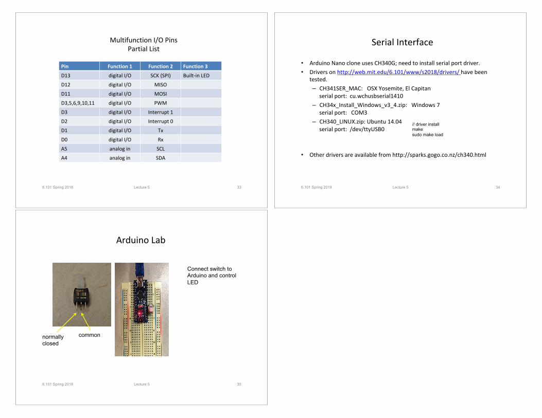
MultifunctionI/OPinsPartialList
Pin Function1 Function2 Function3
D13 digitalI/O SCK(SPI) Built-inLED
D12 digitalI/O MISO
D11 digitalI/O MOSI
D3,5,6,9,10,11 digitalI/O PWM
D3 digitalI/O Interrupt1
D2 digitalI/O Interrupt0
D1 digitalI/O Tx
D0 digitalI/O Rx
A5 analogin SCL
A4 analogin SDA
6.101 Spring 2018 Lecture 5 33
SerialInterface
• ArduinoNanocloneusesCH340G;needtoinstallserialportdriver.• Driversonhttp://web.mit.edu/6.101/www/s2018/drivers/havebeen
tested.– CH341SER_MAC:OSXYosemite,ElCapitan
serialport:cu.wchusbserial1410– CH34x_Install_Windows_v3_4.zip:Windows7
serialport:COM3– CH340_LINUX.zip:Ubuntu14.04
serialport:/dev/ttyUSB0
• Otherdriversareavailablefromhttp://sparks.gogo.co.nz/ch340.html
6.101 Spring 2018 Lecture 5 34
// driver install make sudo make load
ArduinoLab
6.101 Spring 2018 Lecture 5 35
common normally closed
Connect switch to Arduino and control LED

![BJT Circuits Limitations LTspiceTransistor Configurations 6.101 Spring 2020 Lecture 4 3 +15V + V in V OUT-R L R 1 + + R 2 [a] Common Emitter Amplifier [b] Common Collector [Emitter](https://img.dokumen.tips/doc/110x75/5fb86d5b50c3f54786723a2e/bjt-circuits-limitations-ltspice-transistor-configurations-6101-spring-2020-lecture.jpg)