Embed Size (px)
Citation preview
HOMEWORK 5 CMPEN 411Due: 2/28/2012 11:30pm
Learning ObjectiveUse the VLSI CAD tools to design and implement a dual port RAM register file circuit and analyze it.
InstructionThis semester, we are building a simple microprocessor shown below. It is an 8-bit RISC processor, its full description and specification is posted at: http://www.cse.psu.edu/~kyusun/class/cmpen471/11f/hw/pj7/pj7.html One of the central component is the dual port RAM used as a register file. For this homework, implement the 8-register dual port RAM circuit and analyze it. Read all of the following instructions before starting the design.
An 8 bit RISC Microprocessor Data Path

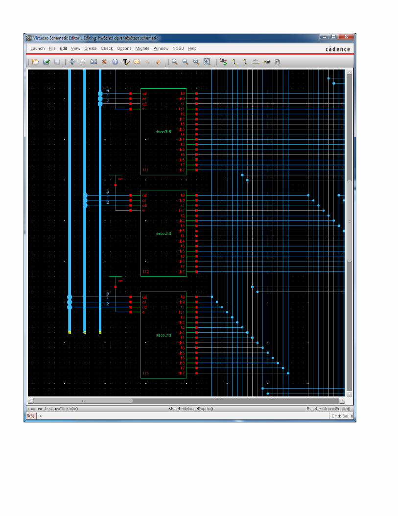
1. Dual port RAM with 8 words is shown below. Implement the dual port RAM but with only 8 words. A word is an 8-bit data in this case. There are two output ports (port A for dat1 and port B for dat2) and one input port (dat0). Technically it is a Tri port RAM but we call it dual port due to its two output ports. Given an address, the address decoder generates the selection signal, only one word is selected in each port.
Dual Port RAM

2. The Dual port RAM word with 8 D-flip flops is shown below. One can update the 8-bit register design of the Homework 3 with two tri-state inverting buffer, the port A (ad<7:0>) is controlled by the enable signal sa and the port B (bd<7:0>) is controlled by the enable signal sb.
Dual Port RAM Word

3. A 3-to-8 address decoder is shown below. A 3-bit address selects one out of 8 output signal to be active. The signal e en-ables or dis-ables the output signal.
4. Using the Cadence tool Virtuoso, design the 8-word 8-bit dual port RAM circuit schematic and layout. The design must be free from the DRC errors and pass the LVS checking.
5. To verify the functioning, design the Hspice simulation files: .hsp, .s, and .sp files. Your simulation output must show address decoder outputs and the port data lines. The port A and port B must include 10fF load capacitors, one in each bit line. Design your .hsp file to write to each location and then read from each location.
6. What is the write time? What are the write setup time and write hold time? What is the worst case read time? Why does it take so long? How can we make it faster? Design the .hsp file to demonstrate the fastest write and
e

read times of the dual port RAM while maintaining correct output result. What limits the maximum speed of operation? Show the simulation plot to substantiate your answer.
7. How many transistors are used in your 8-word 8-bit dual port RAM design?
8. Did you use static, dynamic, or pass transistor logic?
9. Are there any errors in schematic?
10. Is there an error in layout? Does your layout pass the DRC checking without errors?
11. Is there a miss match on the schematic versus layout? Does your design pass the LVS checking without errors?
12. Extract the circuit from the layout including the parasitic capacitances. Then hspice simulate the extracted circuit netlist. Placing 10fF load capacitors on the outputs, what is the worst case output signal rise time, fall time, and delay time? The worst case delay time is from which input to which output? Is the worst case delay time due to write time or read time?Worst case delay time: T = ______ nSec.
13. What is the total layout height and width? What is the total layout area measured in um**2? Area: A = ______ um**2
14. What is the AT**2 measure of your design? AT**2 = ___________ um**2 nSec**2
15. Use hierarchical design method to manage design complexity. That is, design simple cells and design top cell which combines simple cells. The Cadence tool Virtuoso assumes all design is done this way, uses cellview to manage cells.
16. Homework 5 preparation: Create a directory hw5yourlastname under c411 directory (assuming you have c411 directory in your home for this class). Change the current directory to hw5yourlastname. Set up the directory for a new Cadence Virtuoso library. Then start the hw5 design project. For example, my hw5 directory will be hw5choi and I will be running the following unix commands right after I login to my account:
% cd c411% mkdir hw5choi% cd hw5choi% runcds% virtuoso &
You can follow the same except that you need to use your last name after 'hw5'. Collect all the components in this directory, it will be 'tar' and zipped, turn-in to the instructor for grading. This way, you can collect all the files within the hw5yourlastname directory and it will allow the grading. Otherwise, any missing files may cause your design verification for grade to fail. You may lose points if your turned-in hw5 design files cannot be verified by grader.
17. Create a hw5 report file hw5yourlastname.doc and include captured image of layout and the simulation results. Add your explanations and comments. On the Linux machines in room 218 IST, one can use 'openoffice.org' program for the document creating and editing, and use 'gimp' program for the image capture and processing from the screen.
18. The hw5 report file must also include the answers to the questions.
19. The hw5 report file can be in .doc or .pdf, must include a cover page for student information such as 'CMPEN 411’, ‘Homework 5’, your name, etc. The sample format of the hw5 report file is posted: Sample hw5 Report

20. Create a tarred zip file of your hw5yourlastname directory in c411 directory. It will contain the schematics, symbols, layouts, .hsp, .sp files, and .doc report file. In your c411 directory, use the following unix commands
% tar -czvf hw5yourlastname.tgz hw5yourlatname
to create a tarred zip file of hw5yourlastname library. For example,
% tar -czvf hw5choi.tgz hw5choi
will archive the directory hw5choi and create a zipped file hw5choi.tgz in my c411 project directory.
You may want to delete .tr0 files before zipping, for their sizes are usually large.
21. Turn-in your project zip file through Penn State ANGEL. Deposit your zip file into the Homework 5 DropBox under CLASS tab in CMPEN 411 Course.
22. Make sure that you include all the files necessary into your project folder, in order to verify for grading. Turn-in your project before 11:30pm on the due date.
More pictures on the next pages.