Embed Size (px)
Citation preview

Fikeraddis Elias Lemma
Knee Angle Measurement for Knee Implants
Helsinki Metropolia University of Applied Sciences
Bachelor of Engineering
Electronics
Thesis
October 2015

Author(s)
Title
Number of Pages
Date
Fikeraddis Lemma
Knee Angle Measurement
37 pages + 8 appendices
06 October 2015
Degree
Bachelor of Engineering
Degree Programme
Electronics
Instructor
Drs.Ing. Patrick Pelgrims (Project Manager)
Matti Fischer , Principal Lecturer (Project Manager)
The Knee angle project was carried out at Thomas More University in Belgium. The aim of the project was to measure the change in rotational angle of the knee prosthesis and create a stable data reading between sensors, ADC (analog digital converter), microcontroller and a wireless module. In addition, the project was aimed at presenting readable and understandable code flow with a development of better performance. The Knee measurement system for knee implant reduces knee replacement complications and expenses. Also, it provides closer control and visualization of knee prosthesis so that it will be easy to improve patient health. The thesis explains the devices and methods used in this project.
The development of the knee angle measurement system comprised of four parts; Analog front end, sensor part, microcontroller and wireless module. Hardware devices and software applications were used in testing and analyzing the results, for example- Saleae logic analyzer, USB to UART converter and LabVIEW.
The project showed the expected result with complete functionality of the wireless module and the sensor with a stable change in amplitude. The analog to digital converter had minor SPI timing problems that can be solved by a closer study of the timing properties of SPI in the ADS.
Keywords
Human Joint, ADS1296,nRF24L01, Microcontroller, SPI,
Sensors

Contents
1 Introduction
2 Human Knee Joint
2.1 Knee Arthritis
2.1.1 Rheumatoid Arthritis
2.1.2 Osteoarthritis
2.2 Knee Replacement (Arthroplasty)
3 Theoretical Backgrounds of the System
4 Components Used In Knee Angle Measurement System
4.1 Magnet S-05-08-N
4.2 Sensor Units: AMR Sensor Principle
4.2.1 HMC1512
4.2.2 LIS3MDL Digital Sensor
4.2.3 LIS3MDL Adapter Board (STEVAL-MKI137V1)
4.3 Analog Front End
4.3.1 ADS1296
4.3.2 Operation Principle
4.3.3 Interfacing ADS1296
4.4 Microcontroller: MSP430
4.4.1 Operation Principles and Mode
4.4.2 Clock System
4.4.3 Enhanced Universal Serial Communication Interface-SPI Mode
4.4.4 MSP-FET430UIF Universal Programmer
4.5 Wireless Module: nRF24L01
4.5.1 Hardware Features
4.5.2 Interfacing the nRF24L01
4.5.3 Transmitter and Receiver

5 Comparison of the System
5.1 Hardware and Software
5.2 Power Consumption
6 Testing Devices and Results of the System
6.1 Saleae Logic Analyzer
6.2 MCP2200 (USB 2.0 to UART Protocol Converter with GPIO)
6.2.1 Real Term
6.3 LabVIEW
7 Conclusions and Discussion
References
Appendices
Appendix 1. Measurements set up including Transmitter and Receiver ends
Appendix 2. QFN24 Package design for the Microcontroller
Appendix 3. Saleae Logic Analyzer test results
Appendix 4.1 Four different magnet position setups
Appendix 4. 2 Four different magnet position setups
Appendix 4.3 Magnetic data taken at 4 GAUSS for 12 samples
Appendix 4.4 Graphical representation of the four setups in XYZ
Appendix 5.Test result in LabVIEW development software

Acronyms
AFE Analog Front End
ASIC Application Specific Integrated Circuit
ADC Analog Digital Converter
AMR Anisotropic Magnet Resistance
ULP Ultralow Power
MCU Microcontroller
SPI Serial Peripheral Interface
GND Ground
I2C Inter Integrated Circuit
PE Polyethylene Insert
PGA Programmable Gate Amplifiers
FP Femoral Part
TP Tibial Part
LPM Low Power Mode
eUSCI Enhanced Universal Serial
Communication Interface

1
1 Introduction
Knee angle Measurement started at Thomas More University with the collaboration of EmSys
group that aim in development and implementation of embedded systems. The project was
started between two students from Thomas More University (Kevin Sebrechts and Sven
Sleeckx) and continued in improving the system.
This project is a part of a knee angle measurement system project for artificial knee implants,
consisting of a Knee Unit: an in vivo system which would be part of knee implants; A Data
Logger: an outside system used to receive data wirelessly from the Knee Unit; and an outside
power supply unit which would supply power wirelessly to the in vivo Knee Unit.
The target system for this project is the in vivo Knee Unit which consists of different peripheral
units such as: a sensor unit (HMC1512), analog front end (AFE) ADS1296, a microcontroller
(MSP430FR5724) unit and a wireless communication module (nRF24L01).
The main focus of this paper is the explanation of a C software code which was modified
according to a new version of printed circuit board for the Knee Unit. Power efficiency is an
essential part of the entire scheme since the plan is to use an outside vivo wireless inductive
power supply unit in the future. In the new version of the code various programming techniques
were used to save power resulting in a more energy efficient system. These measures include:
changing the software SPI communication used in the previous software to hardware peripheral
SPI; using interrupts to enter to low power mode and sleep the processor; and taking advantage
of the ULP(Ultra low power) advisor of code composer studio for modifying the code
accordingly. After the communication; the project continued with adopting a new sensor
(LIS3MDL) in reducing the size of our PCB.

2
2 Human Knee Joint
The knee is a joint formed to sustain and move bones, ligaments and tendons. It is the largest
joint in the human body and formed by the assertion of a femur in the upper part of knee and
tibia in the lower leg.
The knee joint shown below in figure 1 is one of the important and strongest parts of human
body. It supports human body weight and allows movement of the lower leg relative to our thigh.
Our day to day activities, including running, walking, standing and sitting depend on this joint.
Figure 1. Human Knee Joint (Copied from Cape Town knee surgery [1]).
Femur - is the strongest and heaviest bone that supports the entire human body. Our body
weight is supported by femur while doing different activities such as running, sitting, walking and
jumping.
Tibia (Shinbone) – is the stronger and larger one of the two lower leg bones. Lower leg and foot
muscles are anchored to the tibia. In the same manner, it is essential for supporting body
weight and various movement activities; such as running, jumping, sitting and walking.
Fibula – is the long, thin and lateral bone of the lower leg. Fibula supports lower leg muscles
and helps in stabilizing an ankle. Because of its thin size, its function relays on supporting tibia.

3
Tibia, femur and fibula are closed with articular cartilage, which is an elastic material that act as
shock absorber and grant our knee to move calmly. This pivotal joint is immersed in synovial
fluid and allows six-degree of freedom motion. Figure 2 shows knee joint rotation in three
anatomical planes and translation in three anatomical planes
Figure 2. Knee movement anatomical planes (Copied from Tom's Physiotherapy Blog
[2]).
The triangular shaped bone on the front side of knee that protects the knee joint is called Patella
(knee cap). The Human knee joint can face enormous knee joint problems due to different reasons.
2.1 Knee Arthritis
Musculoskeletal (Rheumatic) diseases consist of over 150 diseases categorized under Joint
diseases, physical disability, spinal disorder and conditions happening from trauma.
These musculoskeletal diseases cause a high rate of disability and risk of a proper functioning
of day to day activities that affect personal life. The common knee joint diseases are listed and
discussed below.

4
2.1.1 Rheumatoid Arthritis
Arthritis is one of the known diseases that affect joints, connective tissues, fibrous tissue,
muscles and tendons which occur during early childhood. It causes disability and deformity of
joints. It is commonly visible in women in developed countries with a rate varying between 0.3
% and 1 %.
2.1.2 Osteoarthritis
Degenerative joint disease is another name for osteoarthritis that creates a breakdown of
articular cartilages. It mostly happens in old people and comes as a consequence of aging.
Force resistant joints face osteoarthritis including hips, knees, fingers and lower spine regions.
The data from world health organization states osteoarthritis as one of the most disabling
diseases worldwide with an estimation rate of 9.6 % of men and 18.0 % of women aged above
60 years showing significant osteoarthritis.
2.2 Knee Replacement (Arthroplasty)
The knee joint is exposed to a developmental joint disease and injuries due to workload and
shocks. In order to help injuries and developmental disorders, knee replacement should be
carried.
Knee replacement (knee arthroplasty) is a surgical procedure carried out to replace fully or
partially the weight bearing part of the knee with prosthetic part
(artificial leg).
Knee Prosthesis consists of a femoral part, a tibia part and polyethylene which is inserted
between the femoral and tibia part. The procedure differs depending on the fixation, material
and design. An extra careful procedure is needed in knee prosthesis procedures; misalignment,
ligament imbalance, loosening and a problem in the polyethylene causes an adverse effect on
the replacement.

5
Figure 3. Knee Prosthesis design (Copied from AESCULAP Implant Systems [3])
In knee prosthesis femur and tibia are the most important joints in knee joint. Figure 3 shows
knee replacement design with femoral part attached to the lower end of femur and the tibial
component attached to the top end of tibia to hold the PE component.
Figure 4 below describes the upper and lower part of knee prosthesis metal parts. The upper
part of the prosthesis has a metal curved around the Femur, the lower part consists of PE
(polyethylene insert) to be placed between the femur and tibia to help as a cartilage and
another metal part to be secured to the tibia.

6
Figure 4. The above figure shows Knee prosthesis descriptions and
F.I.R.S.T.knee prosthesis by Symbios Orthopédie SA (Copied from Arash Arami (2014) [5, 95]).
There are two types of knee replacements
• Total knee replacement that includes both (left and right) sides of knee replacement.
• Partial knee replacement is where only one side of the knee is damaged or diseased
and need a knee replacement.
Artificial prosthesis relieves patient pain and allows better movement of the knee. A study
shows that more than 60,000 knee replacement surgeries are held in the USA and over 70,000
in England and Wales. This often occurs on aged people over 65 years.
Total knee replacement is a more complex procedure than partial knee replacement and these
procedures require precise measurements and removal of the damaged or diseased part of the
bones. The artificial knee is implanted by building each component at a time to free complexity.

7
3 Theoretical Backgrounds of the System
As explained in the introduction section, this project focused on a knee angle measurement in
an artificial leg. Figure 5 shows different system integrations used while working on the knee
angle measurement project: Linear/Angular/Rotational displacement sensors (HMC1512), low
power 8 channel 24 bit analog front-end ADS1296, MSP430F57xx family mixed signal
microcontroller (MSP4305724) and nRF24L01+ single chip Transceiver. The operation principle
of the whole system is explained step by step as follows.
Figure 5. Block diagram of the system
At first the magneto-resistive sensors sense the strength of the magnetic field which varies
relative to the position of the magnet in reference to the sensors. Then this data collected by the
sensors is fed to the ADS for amplification and ADC conversion. After conversion, the analog
data received from the sensors is presented in a 24 bit format and is fed to the MSP
microcontroller via SPI bus.
Afterwards, the 24 bit data from the analog front end is modified by the microcontroller to 16 bit
format and is sent to the wireless module (nRF24L01+) via SPI bus for wireless transmission.
The Knee angle measurement project continues in replacing HMC1512 magnetic displacement
sensor by LIS3MDL digital sensor.
The communication of the sensors to AFE (analog front end) has been configured in SPI
interface has been used while replacing the new sensor (LIS3MDl) to communicate with
MSP430. The position of the sensors is an important aspect of getting proper data reading.

8
Figure 6 shows the rotation of knee joint and position of the three sensors. The sensor
attachment position has a direct effect on the measurement accuracy so extra careful
procedures should be taken.
Figure 6. Sensor positioning in human knee joint (Copied from Knee angle measurement thesis
documentation [4]).
The sensor is positioned in the polyethylene insert (plastic) part of the replacement and the
magnet in the femoral part of the human knee joint.
Figure 7. (a) AMR sensor inside PE. (b) Magnet in FP and AMR sensor position (Copied from
Arash Arami (2014) [5, 95]).
Figure 7 above implies position of the magnet and the three sensors. The magnet is situated in
the femoral part and the sensors on the PCB situated on the PE (Polyethylene Insert).

9
4 Components Used In Knee Angle Measurement System
Various unit systems have been used while working on knee angle measurement project.
1. Magnet
2. Sensor Unit
3. Analog Front End
4. Microcontroller
5. Wireless Module
This section discusses these system units in brief and appendix 1shows the measurement
setup together with receiver and transmitter part of the wireless module
4.1 Magnet: S-05-08-N
The S-05-08-N is a very small magnet with a diameter of 5 mm and height of 8.47 mm. This
strong rod magnet has magnetization level of N45 in which the letter "N" indicate the maximum
working temperature of the magnet in this case 80 °C and the number indicating the maximum
energy product of the magnet.
The maximum amount of magnetic energy stored in a magnet can be measured to detect the
maximum energy product of a magnet with a unit of kJ/m3 or MGOe (MegaGauss-Oersted).
Considering S-05-08-N, it has a magnetization of N45 telling a maximum temperature of 80 °C
with energy product level of 45 kJ/m3 or 358 MGOe.
4.2 Sensor Unit: AMR sensors principle
AMR sensors have Si or glass board and a thin film of ferromagnetic metals (like Ni and Fe) on
the board. Figure 8 below shows decrease in resistance with the strength of magnetic field
when current (I) is applied to the ferromagnetic thin film metal in the direction of Y and magnetic
field (H) to the direction of X that is vertical to the current direction.

10
Figure 8. AMR sensors (Copied from KOHDEN [12]).
4.2.1 Linear/Angular/Rotary Displacement Sensor
Honeywell’s HMC1512 is a high resolution, low power sensor with the ability of measuring the
angle direction of a magnetic field from a magnet with a wide angular range of ±90° with <0.05
resolution and can give full scale output ranges of 120 mV with 5V of power supply.
It follows AMR sensing principle which changes the value of the magnetic resistance according
to the strength of the magnetic field.
Figure 9 shows the sensor in the form of Wheatstone bridge that measure magnetic field
direction. R (resistor) of the four resistors has the same value and the power supply (Vs)
sources current to flow through the resistors in the direction as shown below in figure 9 for each
resistor.
Figure 9. Basic sensor bridge schematics (Copied from Honeywell [13]).
The system consists of three HMC1512 magnetic sensors aligned in T shape to detect the
relative angle of the magnet to a different axis. The human knee can move in three different
axes, thus we should also be able to measure this angle relative to those.

11
4.2.2 LIS3MDL Digital Output Magnetic Sensor
The project continues with a plan of replacing the sensor with an ultra-low power, high
performance 3-axis magnetometer; LIS3MDL. It has the same working principle, three sensors
and analog to digital converter with a central unit microcontroller in communication with a
wireless module (nRF24L01).
LIS3MDL is a 16-bit data output sensor with a wide supply voltage of 1.9 - 3.6 v range. It has
selectable magnetic full scale allowing selectable conversion mode for better performance. It
can be configured in SPI or I2C mode depending on user selection moreover, it allows self -test
for a proper operation of the sensor.
LIS3MDL sensor is preferable due to its advantage in allowing selectable test conditions for
sensitivity test, wide supply voltage range and easy device identification by configuring the
WHO_AM_I register for self-test.
Figure 10. Showing electrical connections of LIS3MDL (Copied from
STMicroelectronics datasheet [14]).
12
External capacitors are needed for proper functioning of the sensor; as shown from figure 10
schematic. It is possible to solder the external capacitor as stated, but there is a readymade
adapter board with all the necessary features.
The configuration of LIS3MDL is important for proper functioning of the sensor. The control
registers should be set to use the features. Mainly CTRL_REG1, CTRL_REG2, CTRL_REG3,
CTRL_REG4 and CTRL_REG5 should be used. LIS3MDL allows both SPI and I2C
configuration with different pin descriptions. The I2C interface only acquires two signal lines, a
serial clock line and a data line. In addition to the pins, there are other necessary modes and
requirement to fulfill. In this paper, only SPI interface will be discussed.
The control registers have specific applications.CTRL_REG1 allows configuring the operational
mode and output data rate with different frequency values according to usage. Enabling the
FAST ODR (output data rate) from this register is important in selecting the proper ODR (output
data rate) and OM (operational mode).The data rate configuration depends on the output data
rate and on the FAST output data rate selection with operational mode preferences (low power,
medium power, high power and ultrahigh power) which is stated on the datasheet of the sensor.
Focusing on Low power was an important aspect but due to the frequency requirement, the
needed ODR (operational data rate in Hz) shifted to UHP with an ODR of 155.
To adjust the measured input dynamic range of the device to the amplitude of the magnetic
field, configuring CTRL_REG2 is a must. The LIS3MDL sensor allows variant choices with gain
at 16-bit. All the full-scale selections were taken to visualize the performance of the sensor.
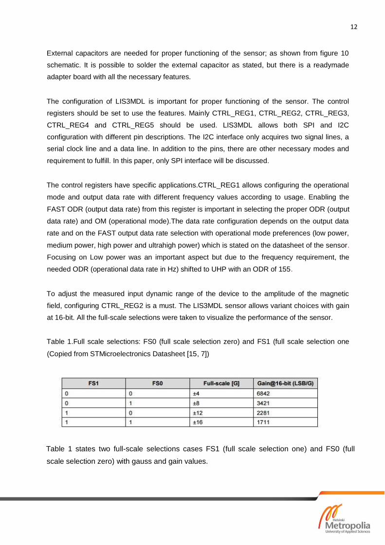
Table 1.Full scale selections: FS0 (full scale selection zero) and FS1 (full scale selection one
(Copied from STMicroelectronics Datasheet [15, 7])
Table 1 states two full-scale selections cases FS1 (full scale selection one) and FS0 (full
scale selection zero) with gauss and gain values.
13
This helps to evaluate the input dynamic state of the device to the amplitude of the magnetic
field to be measured. In this project all full scale levels were tested to visualize the magnetic
field of the magnet. The system mode runs in continuous measurement of data and writes the
measured data in specific data output registers for a read. The data read has been configured
using the STATUS_REG to examine the lower and higher end of the three axes (X, Y and Z).
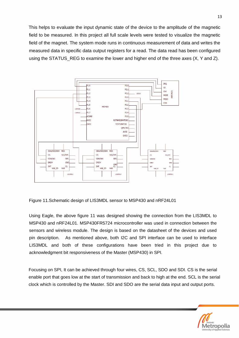
Figure 11.Schematic design of LIS3MDL sensor to MSP430 and nRF24L01
Using Eagle, the above figure 11 was designed showing the connection from the LIS3MDL to
MSP430 and nRF24L01. MSP430FR5724 microcontroller was used in connection between the
sensors and wireless module. The design is based on the datasheet of the devices and used
pin description. As mentioned above, both I2C and SPI interface can be used to interface
LIS3MDL and both of these configurations have been tried in this project due to
acknowledgment bit responsiveness of the Master (MSP430) in SPI.
Focusing on SPI, It can be achieved through four wires, CS, SCL, SDO and SDI. CS is the serial
enable port that goes low at the start of transmission and back to high at the end. SCL is the serial
clock which is controlled by the Master. SDI and SDO are the serial data input and output ports.

14
Figure 12.Read and write protocol of LIS3MDl in SPI (Copied from
STMelectronics datasheet [14]).
The above figure 12 describes the data read and writes protocol for SPI interface.
The SPI read and write command is carried out with 16 bit clock pulses.
The RW bit (bit 0) indicates two conditions when RW is 0, data is written into the device that is
DI (7:0).On the other hand when 1, data is read from the device DO (7:0).MS bit also has two
possible cases when 0, it indicates the address stays unchanged in multiple read/write
commands and when 1, the addresses will be auto incremented in multiple read/write. The AD
(5:0) shows the address of the registers. Due to lack of information on the sensor functionality
and configuration in SPI, I2C interface has been tried to check the normal functionality of the
LIS3MDL.
There are four important terms to understand the functionality of the sensor in I2C interface.
Transmitter; the device that send data to the bus, Receiver; the device that receives data from
the bus, Master; the device responsible to initiate the transfer, generate clock signal and also
halt the transfer and lastly, Slave; which can be addressed by the master. LIS3MDL provides
self-test features in order to test the sensor by enabling the test bit of CTRL_REG1 and also
consists of temperature sensor suitable in temperature measurement in the same control
register.

15
4.2.3 LIS3MDL adapter board (STEVAL-MKI137V1)
The adapter board is used for better usage and functionality of the LIS3MDL sensor. In addition,
it has all the needed decoupling capacitors and power line for proper operation of the sensor. It
is usable for the DIL24 socket and adaptable with an STEVAL-MK137V1 motherboard.
The communication started in configuring only one sensor for understanding the working
principle and continued on adapting SPI interface. The electrical connection of the sensor was
used according to the datasheet also shown below in figure 13. Due to unknown reasons; the
sensor could not function as expected. As a result, it was necessary to change the sensor
because of hardware failure expectations but the second sensor showed the same result. I2C
interfacing has also been adapted to test the operation of LIS3MDL nevertheless the sensor
could not pass the self-test.
Figure 13.Schematics of STEVAL-MKI137V1 (Copied from STMelectronics, STEVAL-
MKI137V1 LIS3MDL adapter board [16]).
Thus, LIS3MDL adapter board solved the entire problem and the system was able to pass the
self-test and create communication between the sensor and microcontroller. The
STMelectronics adapter board application note has a precise electrical connection with
unambiguous pin arrangement.

16
4.3 Analog Front End
It is a circuitry that consists of OPAMPs, filters, ASIC and other necessary electronic functional
blocks to interface different sensors to ADC or microcontroller. ADS1296 is one of Texas
Instrument’s AFE (analog front end) used in the health monitoring. It has been used to interface
the sensors with a microcontroller, the central unit which control sensors data storage and
communications.
4.3.1 ADS1296
This is a multichannel, low power ADC with built in PGA, internal reference and onboard
oscillator giving 24 bits of data output per channel in binary twos complement with MSB first.
The data rate of the ADC in ADS1296 extends from 250 SPS to 32 kSPS. It has four GPIO pins
for general use allowing the digital I/O pins to be individually configurable as either input or
output in GPIO register. Communication is through SPI interface. ADS1296 contain on-chip
temperature sensor which was not used in this project though it can be configured accordingly
for a specific application. The ADC in ADS1296 can measure up to 6 differential voltages with
the ability to display 6 channels and this was one important reason to select the ADC in the
ADS1296 and higher data output rate for better resolution.
4.3.2 Operation Principle
To read the analog data from the sensors, the ADC in ADS1296 is an important electronics
system. The ADC converts analog data to digital data because of the microcontroller
processors ability to read only digital data, i.e.1s and 0s.
The processor in the microcontroller is not able to do anything with the Analog data that may be
sent to it by a device. In order to read the data, the ADC is responsible in changing analog data
to digital data. There are four SPI interface signal pins to build communication between the
ADC and microcontroller: CS (chip select), SCLK (Serial clock), DIN (Data IN) and DOUT (Data
OUT). The chip select, as the name describes, selects the chip for SPI communication and
stays low until the end of the communication.
It is always advisable to hold the chip select for four or more clock cycles before taking it back to
high. The serial clock (SCLK) is useful for transmission of command and data from the ADS.
Once chip select is low, the device starts to execute the command every eight serial clocks.
The data input including the SCLK is used to communicate with the ADS and the data out
(DOUT) with the SCLK which is the serial clock is used to register and read data from the ADS.

17
4.3.3 Interfacing ADS1296
The analog digital converter in ADS1296 gives data rates ranging from 250 SPS to 32 kSPS.
Texas instruments ADS1296 has four general purpose GPIO pins and SPI configuration were
adopted for communication.
As stated earlier in the introduction of ADS1296, it produces output data of twos complement
form with 24 bits of data for each channel allowing the most significant bit to be the first data
out. SPI configuration helps in writing, reading, converting and controlling data. The other
important pin is DRDY (Data Ready) pin that points when data is ready. To understand the
operation of this GPIO pins, let’s look at figure 19 below.
Figure 14.SPI Bus data Output for ADS1298 (Copied from Texas Instruments
[18]).
In the operation of the ADS, the DRDY (data ready) goes low means ready data exists and
shifted out on the rising edge of SCLK (clock) also because of continuous conversion mode
configuration for this project, it shows when data is available. From figure 14, it is
understandable that the CS (chip select) selects the ADS for communication. When CS goes
low, communication starts and stays low until the end of the communication. The SPI
initialization has been configured in the manner of the ADS CLK and ADS MISO as output and
ADS MISO as input moreover pull up resistor were initialized. The DOUT (data out) line shows
the status register value and output data for selected channels. The ADS1296 used in this
project has 6 channels which means data out line shows status register value and data out for
six channels.
The data transmission follows MSB first, Master mode, Synchronous 3 wire SPI, ACLK clock
source and data is captured on the first UCLK edge and change on the following edge.

18
Figure 15.Opcodes and command
Opcodes (operational codes) are used to configure and send commands of the ADS. Figure 15
shows an opcode with an address 0x02 CONFIG2 (configuration register) and the number of
registers to read and write.
4.4 Microcontroller: MSP430
It is an embedded system consisting of programmable peripherals, memory and processor for
various applications for example: phones, automobiles, machines, medical devices and other
embedded systems. Microcontrollers differ in their type; bits, flash size, RAM size, speed,
supply voltage and a number of input/output lines categorize MCUs in different types.
Programmable microcontroller’s conception is to use it in embedded application which is being
used widely and in this project.
4.4.1 Operation Principle and Modes
The Texas Instruments MSP430FR5724 ultra low power microcontroller has been used while
working on this project. It features ultra-low power 16-bit MSP430 CPU, nonvolatile memory,
10-bit A/D converter, 16 channel comparator, serial channel allowing SPI, I2C and UART
protocol, real-time clock and other peripheral for different applications. MSP430 has one active
mode and configurable low power modes LPM0, LPM1, LPM2, LPM3 and LPM4.
Once an interrupt happens, the device will exit from low power mode and perform its normal
operation and again go back to LPM. The LPMs are necessary and designed to achieve: ultra-
low power, decrease current consumption and speed and data throughput which were the main
aim in working on knee angle measurement project. The configuration of these power modes is
through CPUOFF, OSCOFF, SCG0 and SCG1 mode control bits that are found in SR
(status register).

19
The microcontroller is the central unit in knee angle project. It acts as a bridge between the
sensor and ADS and wireless module. The ADS transfers digitally converted data to the MCU
for process and transmission to the nRF24L01.
4.4.2 Clock System
The microcontroller consists of four system clock signals that allow selecting suitable
performances and low power consumption. It comprises up to five clock sources and figure 16
states the configuration of clock source in relative to the desired performance and power
consumption.
The low-frequency or high-frequency oscillator, internal low power low-frequency oscillator,
internal digitally controlled oscillator (DCOCLK), optional high-frequency oscillator are the
system clock signals for the microcontroller.
There are four system clock signals from the clock system module: ACLK (Auxiliary Clock) – is
software selectable system clock signal. MCLK (Master clock) – is again software selectable
which is used by the CPU and system. The last two are SMCLK (Subsystem Master Clock) and
MODCK (Module Clock).
The DCOCLK; it is an integrated digitally controlled oscillator with three frequency selections
also used as a source for ACLK, MCLK or SMCLK
Figure 16. Control register configuration
The above stated Clock system control registers in figure 16 are used to set the DCO
frequency range, ACLK and source divider which divides the frequency of the ACLK clock
source. Figure 17 shows the configuration of the Control word register and eUSCI_A clock
source select (UCSSELx) bit to control the bit clock.
20
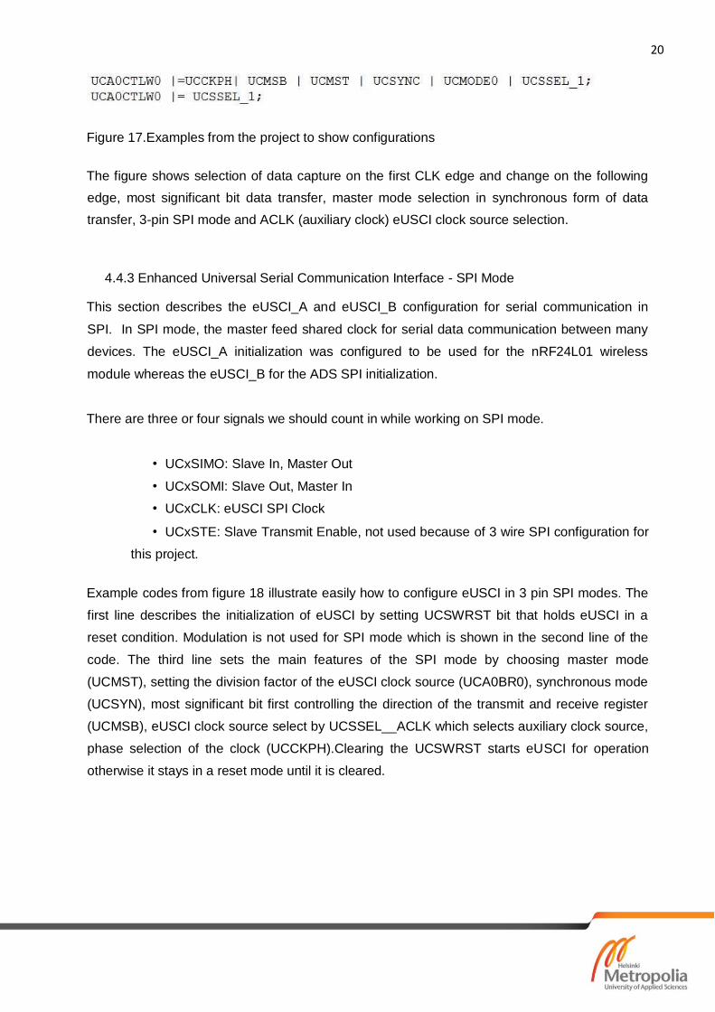
Figure 17.Examples from the project to show configurations
The figure shows selection of data capture on the first CLK edge and change on the following
edge, most significant bit data transfer, master mode selection in synchronous form of data
transfer, 3-pin SPI mode and ACLK (auxiliary clock) eUSCI clock source selection.
4.4.3 Enhanced Universal Serial Communication Interface - SPI Mode
This section describes the eUSCI_A and eUSCI_B configuration for serial communication in
SPI. In SPI mode, the master feed shared clock for serial data communication between many
devices. The eUSCI_A initialization was configured to be used for the nRF24L01 wireless
module whereas the eUSCI_B for the ADS SPI initialization.
There are three or four signals we should count in while working on SPI mode.
• UCxSIMO: Slave In, Master Out
• UCxSOMI: Slave Out, Master In
• UCxCLK: eUSCI SPI Clock
• UCxSTE: Slave Transmit Enable, not used because of 3 wire SPI configuration for
this project.
Example codes from figure 18 illustrate easily how to configure eUSCI in 3 pin SPI modes. The
first line describes the initialization of eUSCI by setting UCSWRST bit that holds eUSCI in a
reset condition. Modulation is not used for SPI mode which is shown in the second line of the
code. The third line sets the main features of the SPI mode by choosing master mode
(UCMST), setting the division factor of the eUSCI clock source (UCA0BR0), synchronous mode
(UCSYN), most significant bit first controlling the direction of the transmit and receive register
(UCMSB), eUSCI clock source select by UCSSEL__ACLK which selects auxiliary clock source,
phase selection of the clock (UCCKPH).Clearing the UCSWRST starts eUSCI for operation
otherwise it stays in a reset mode until it is cleared.
21
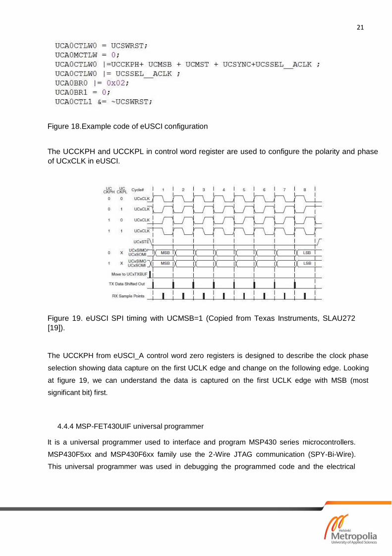
Figure 18.Example code of eUSCI configuration
The UCCKPH and UCCKPL in control word register are used to configure the polarity and phase
of UCxCLK in eUSCI.
Figure 19. eUSCI SPI timing with UCMSB=1 (Copied from Texas Instruments, SLAU272
[19]).
The UCCKPH from eUSCI_A control word zero registers is designed to describe the clock phase
selection showing data capture on the first UCLK edge and change on the following edge. Looking
at figure 19, we can understand the data is captured on the first UCLK edge with MSB (most
significant bit) first.
4.4.4 MSP-FET430UIF universal programmer
It is a universal programmer used to interface and program MSP430 series microcontrollers.
MSP430F5xx and MSP430F6xx family use the 2-Wire JTAG communication (SPY-Bi-Wire).
This universal programmer was used in debugging the programmed code and the electrical

22
connections to the microcontroller were easy due to the QFN2B designed chip by Thomas More
University. Only TEST,
RST, Vcc TOOL and GND as seen from figure 20 were connected to the TEST, RST, Vcc and
GND of the microcontroller for debugging.
Figure 20. Connection guide for 2-Wire JTAG communication (Copied from Texas Instruments
[20]).
The above figure shows the four useful pin connections to the microcontroller for debugging and
appendix 2 shows the designed QFN24B pin configuration based on the microcontroller. The
universal programmer can be seen in appendix 1 in connection to the test board.
4.5 Wireless Module: nRF24L01
The nRF24L01 is a single chip 2.4 GHz transceiver with air data rate up to 2Mbps allowing an
ultra-low power operation. It is used widely in many applications for example in sports watches
and sensors, home and commercial automation, active RFID, others. The SPI configurable
nRF24L01 is an easy wireless module due to its suitable configurable features.
4.5.1 Features and Modes
The nRF24L01 needs six digital signals for data and control interfacing. The IRQ, CE, CSN,
SCK, MOSI, MISO signals.
The IRQ is the interrupt signal pin used by three maskable interrupt sources and the CE (chip
enable) is an active high signal pin to set the nRF24L01 to receiver and transmitter.

23
Table 2. Operational configuration modes for nRF24L01 (copied from Nordic
Semiconductors, nRF24L01 Product Specification) [21, 21]
In this operating mode if the CE is held high the TX FIFO is emptied and all necessary
ACK and possible retransmits are carried out. The transmission continues as long as the TX
FIFO is refilled. If the TX FIFO is empty when the CE is still high, nRF24L01 enters standby-II
mode. In this mode the transmission of a packet is started as soon as the CSN is set high after
an upload (UL) of a packet to TX FIFO. This operating mode pulses the CE high for at least
10μs. This allows one packet to be transmitted. This is the normal operating mode. After the
packet is transmitted, the nRF24L01 enters standby-I mode. (Nordic Semiconductor, nRF24L01
product specification) [21, 21]
4.5.2 Interfacing with nRF24L01
In interfacing the nRF24L01; Vcc, GND, IRQ, CE and four SPI bus pins CSN, SCK, MISO and
MOSI are important. The four SPI interfacing pins are useful for data transmission and
reception showing SPI full-duplex bus property which means sending and accepting data at
once in different lines.
The CSN (chip-select not) is enable pin for the SPI, it is kept high unless SPI command is sent
to the device to get data on the SPI bus from our microcontroller.
MOSI (Master Out Slave In) describes the microcontroller as master and nRF24L01 as a slave
due to nRF24L01 always sending data only when there is a request from the microcontroller
and the master send data to nRF24L01.
MISO (Master In Slave Out) the slave (nRF24L01) sends data according to the request from the
master (Microcontroller). Once the nRF24L01 connection to the microcontroller is set, SPI
interfacing is not a hard task.
Understanding the register instructions and format makes the operation easy. Each register has
an address to write or read and other specific tasks.
24
The W_register allows users to write to the registers in the nRF24L01.The received data packet
is saved in RF_FIFO in RX mode and R_RX_PAYLOAD is useful in checking a received packet
in RX_FIFO register. The W_TX_PAYLOAD is used while sending a packet in TX-mode; the
first step is to send a command byte (A0) which starts the operation in TX-mode and continue
with the payload. The most important thing to consider is to set the same payload for the sender
and receiver to communicate. The CONFIG register is also the other important register to
consider in starting the operation of nRF24L01.It consists of the PWR_UP bit that should be set
to make the nRF24L01 device work; PRIM_RX bit in CONFIG register determines the device as
receiver and transmitter, clearing this bit sets the device as transmitter and on the other way
setting this bit sets the device as receiver.
4.4.3 Transmitter and Receiver
This subsection discusses the transmitter and receiver mode of nRF24L01. The nRF24L01
enters to Rx-mode (receiver mode) while configuring the PWR_UP bit and PRIM_RX bit from
CONFIG register to high. The CE (chip enable) also stays high to set the nRF24L01 to RX
mode.
The RX-mode sets nRF24L01 to receiver mode. The configuration of RX-mode starts with
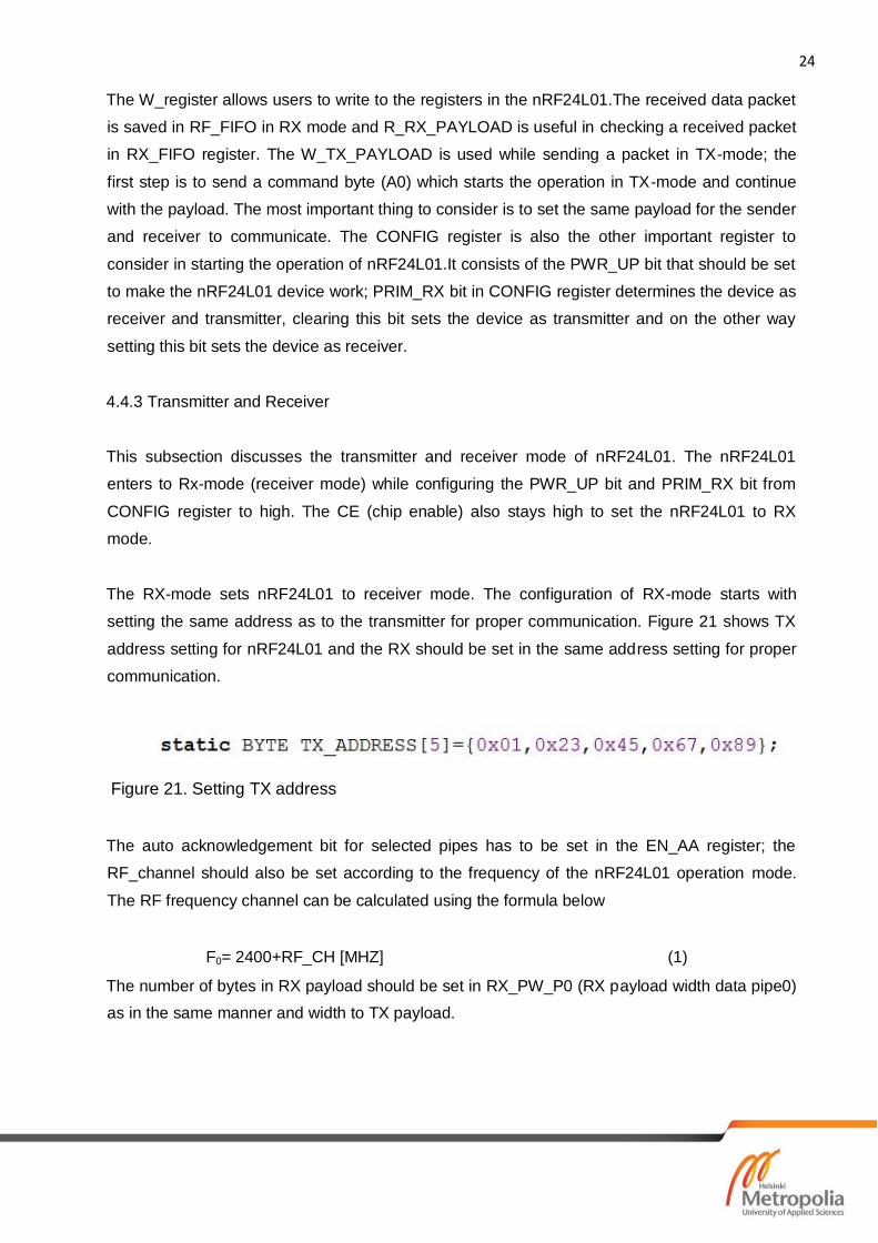
setting the same address as to the transmitter for proper communication. Figure 21 shows TX
address setting for nRF24L01 and the RX should be set in the same address setting for proper
communication.
Figure 21. Setting TX address
The auto acknowledgement bit for selected pipes has to be set in the EN_AA register; the
RF_channel should also be set according to the frequency of the nRF24L01 operation mode.
The RF frequency channel can be calculated using the formula below
F0= 2400+RF_CH [MHZ] (1)
The number of bytes in RX payload should be set in RX_PW_P0 (RX payload width data pipe0)
as in the same manner and width to TX payload.

25
Figure 22. nRF24L01 wireless module RX mode configuration
The SPI_Write_Buf line from figure 22 indicates setting RX address as the same as the TX
device address. The EN_AA register is used to set the auto acknowledgement bit and enable
auto acknowledgment data pipe 0 the same with enable RX address pipe 0 were selected in
this project. The RF_CH register is used to set the RF channel frequency and the RF_SETUP
register is an important register in setting the air data rate with the value of 2Mbps and RF
output power in TX mode as 0dBm. The last line (CE high) enables the RX device.
The receiver and transmitter should be set with the same air data rate for communication. The
nRF24L01 offers 1Mbps and 2Mbps air data rate options. Choosing high air data rate gives
lower average current consumption and due to this advantage 2Mbps was selected while
working on the project. TX-mode as the name implies is the transmitter mode of the chip. The
PWR_UP bit is set high as the same as the RX-mode but the PRIM_RX should be cleared to
enter to TXmode. The TX FIFO payload should be set and importantly the CE (chip select) bit
should stay high for more than 10μs. Table 2 describes an easy way to configure the TX and
RX modes
Figure 23. nRF24L01 wireless module TX mode configuration

26
Figure 23 shows SPI configuration for TX mode of nRF24L01.The first line writes the
TX_Address to nRF24L01 and enables auto acknowledgment pipe0 with auto retransmit delay
of 250us.The CONFIG register sets the PWR_UP bit and enable the cycle redundancy check
(CRC detects error in data packets) to 2 bytes. TX and RX modes have common configuration
features for proper communication. Setting the address, auto acknowledgement, RF channel,
payload width, RF transmit power and data rate, retransmit settings have to have the same
configuration setting and most importantly extra attention to the CONFIG register configuration
of nRF24L01.
5 Comparison
This section compares the systems and devices used in knee angle measurement project. The
project focused on advancing the system for better performance by comparing and drawing
solutions.
5.1 Design and Units
This subsection covers design comparison between the old and new schematic design and
PCB. Figure 24 shows the old designed schematic board and figure
25 shows the new designed schematic board designed by Jurre De Weerdt at Thomas More
University.
Figure 24. Old designed schematic (Copied from EMSYS, Campus De Nayer by Jurre De
Weerdt)

27
The above figure 24 shows the design of the old schematic board with pin arrangements. Only one
SPI line was adopted for both wireless module and analog front end. From the schematic, it is
understandable that P1 and P2 ports are used in interfacing the analog front end and nRF24L01 and
the PJ ports were used for programming the header.
Figure 25. New designed schematic (Copied from EMSYS, Campus De Nayer by Jurre De
Weerdt)
The new schematic design as seen in figure 25 adopts two of the SPI ports to interface the
analog and wireless module. Both the nRF24L01 and ADS has assigned to specific pins
according to their functions. It is very important to check the function of the ports and pins
before assigning them to any function.
Few rearrangements were necessary for the new schematic board, swapping the ADC_DRDY
(ADC data ready) and ADC_RESET (ADC reset) pins due to PJ.1 (Port J pin 1) which the
ADC_DRDY assigned pin inability to support interrupt functions. The other was swapping
ADC_CS and NRF_CSN on pin 3 and 4 of port 1 as a result of pin assignation in the GPIO
ports and pins of the project.
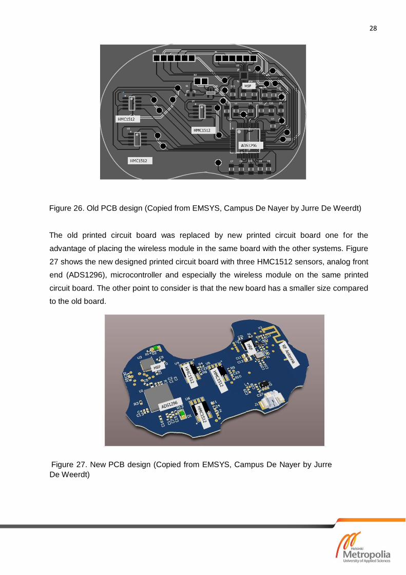
The old and new designed printed circuit boards are another hardware units to compare.
Figure 26 shows the first PCB design of the project consisting three HMC1512 sensors,
ADS1296 (analog front end) and microcontroller. The wireless module was in a separate
board. So the communication goes from the sensors to the ADS then to the MSP and lastly
to the external board that hold the wireless module (NRF).
28
Figure 26. Old PCB design (Copied from EMSYS, Campus De Nayer by Jurre De Weerdt)
The old printed circuit board was replaced by new printed circuit board one for the
advantage of placing the wireless module in the same board with the other systems. Figure
27 shows the new designed printed circuit board with three HMC1512 sensors, analog front
end (ADS1296), microcontroller and especially the wireless module on the same printed
circuit board. The other point to consider is that the new board has a smaller size compared
to the old board.
Figure 27. New PCB design (Copied from EMSYS, Campus De Nayer by Jurre
De Weerdt)

29
Software comparison of the system focuses on SPI adoption of hardware and software
interface. The first work was done in adopting software SPI for the system. Through the
process, changes have been made for example converting the code flow of the software based
SPI to understandable and easy code flow with descriptions. The work continued with adopting
hardware SPI for the system that can handle the data transfer automatically.
5.2 Power Consumption
Low power mode is an advantage to save the current consumption in the process. The previous
work done by one of the student in Thomas More University did not adopt interrupt and LPM
(low power mode) so that it was one idea to use interrupts and low power mode to reduce
current consumption in order to allow the system to rest while doing nothing and go back to
normal operation mode when interrupt happens.
Code composer studio has two ways of code building options which is called Configurations.
The first one is debug configuration, unoptimized way of debugging that maintains the symbolic
debug configuration and secondly release (optimized) configuration. Released configuration
adds options to transform the codes to release mode to make it easier to evaluate the
performance of the optimized code. This feature can be adapted easily through code composer
studio build options.
6 Testing Devices and Results
This section covers the devices used while testing the system and results. All the results
are based on the test performed.
6.1 Saleae Logic Analyzer
It allows user to examine digital signals in electronic projects. This logic analyzer is easy to
use and inexpensive. By plugging the logic analyzer to a computer user can visualize the
digital signals in SPI, I2C, Serial, I-wire and other digital protocols.
The SPI for saleae logic analyzer has four main lines: Clock line, an enable line, master to
slave line and slave to master line. The SPI setting can be adjusted in the right corner of the
logic display.

30
The clock polarity (CPOL) and clock phase (CPHA) are one of the most important factors in
outputting proper signal describing data validity in the clock leading edge or trailing edge.
Figure 28. Saleae logic decodes of SPI (Copied from Saleae [22]).
Figure 28 shows how the saleae logic analyzer display looks like for SPI. It consists of the
EN (enable) or the Slave Select (SS) acts as disabled when 1 and enabled when 0. MOSI
is the master out slave in line showing the master holding the data output (MSB first). MISO
(master in slave out) line shows the master holding the data input line (MSB first) and CLK
is the clock line used by both MOSI and MISO.
This subsection discusses the visualized results from the ADS, nRF24L01 and lastly the
LIS3MDL sensor communication with the whole system.
Figure 29 below shows the nRF24L01 saleae logic result indicating the STATUS register
test result while checking the proper functionality of the wireless module. The 0x2E
hexadecimal format from figure 29 logic display shows value of the STATUS register in the
nRF24L01. The TX_DS pin from the STATUS register is asserted when data is transmitted
on TX. In order to start proper communication, it is advisable to clear this bit and MAX_RT
(maximum number of TX retransmit interrupt) again from the STATUS register to allow
further communication.

31
Figure 29. Saleae Logic analyzer results for nRF24L01 showing the status register in
hexadecimal format every eight clock cycles and other dummy bytes.
The SS (Slave Select) or Enable pin goes low during communication and high at the end
communication. The NFR section from the display box shows the data from the nRF24L01 for
every eight clock cycle in hexadecimal format again in the manner of most significant bit first.
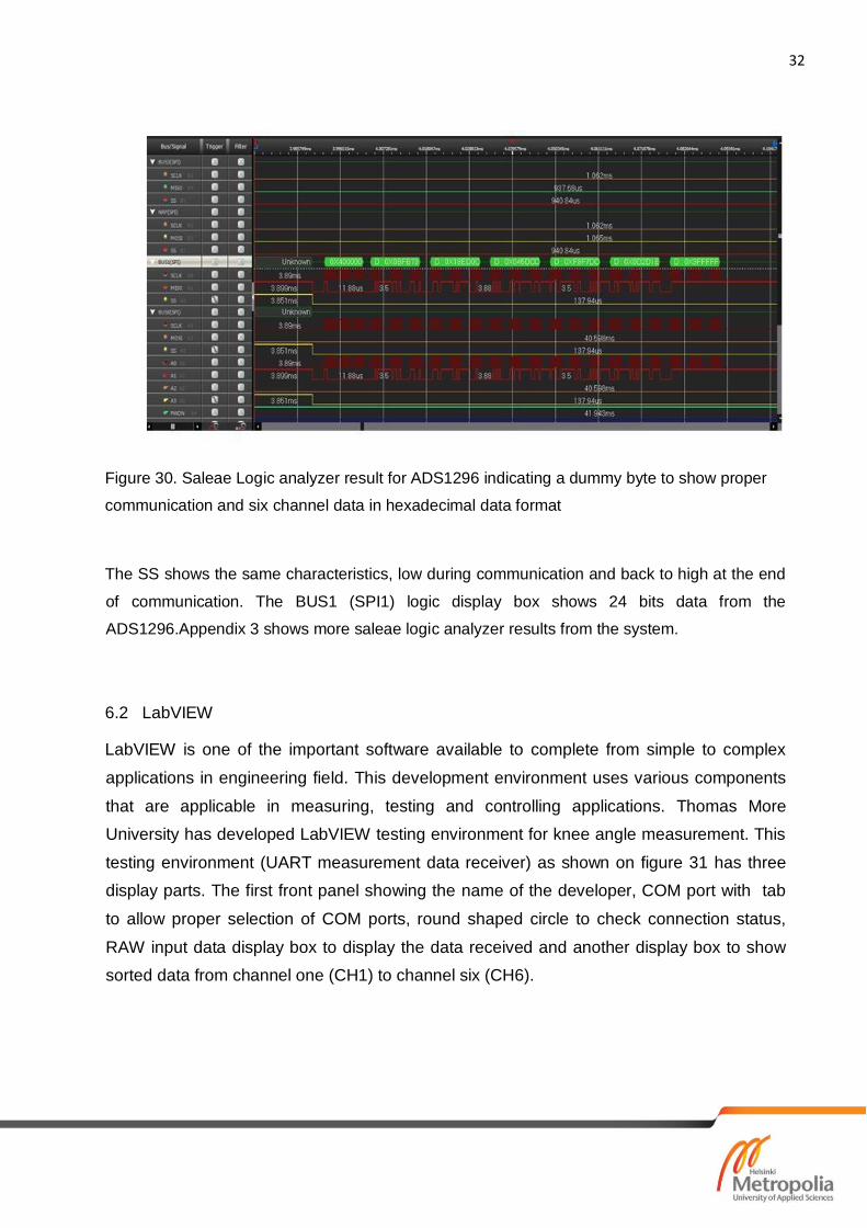
The other test measurement was carried out for ADS1296 to check proper result data. Figure 30
shows the data of the ADS1296 in hexadecimal format with most significant bit with 6 channel
output data. The green boxes shows the data from the ADS, the first hexadecimal value shows a
dummy byte to show the communication is working properly and the other values show the data
out for the six channels in hexadecimal data format for every eight clock cycles.
32
Figure 30. Saleae Logic analyzer result for ADS1296 indicating a dummy byte to show proper
communication and six channel data in hexadecimal data format
The SS shows the same characteristics, low during communication and back to high at the end
of communication. The BUS1 (SPI1) logic display box shows 24 bits data from the
ADS1296.Appendix 3 shows more saleae logic analyzer results from the system.
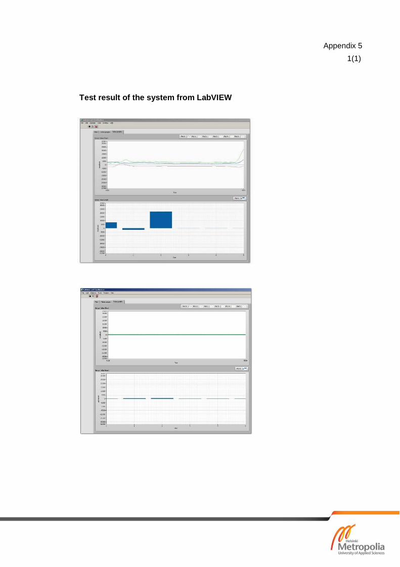
6.2 LabVIEW
LabVIEW is one of the important software available to complete from simple to complex
applications in engineering field. This development environment uses various components
that are applicable in measuring, testing and controlling applications. Thomas More
University has developed LabVIEW testing environment for knee angle measurement. This
testing environment (UART measurement data receiver) as shown on figure 31 has three
display parts. The first front panel showing the name of the developer, COM port with tab
to allow proper selection of COM ports, round shaped circle to check connection status,
RAW input data display box to display the data received and another display box to show
sorted data from channel one (CH1) to channel six (CH6).
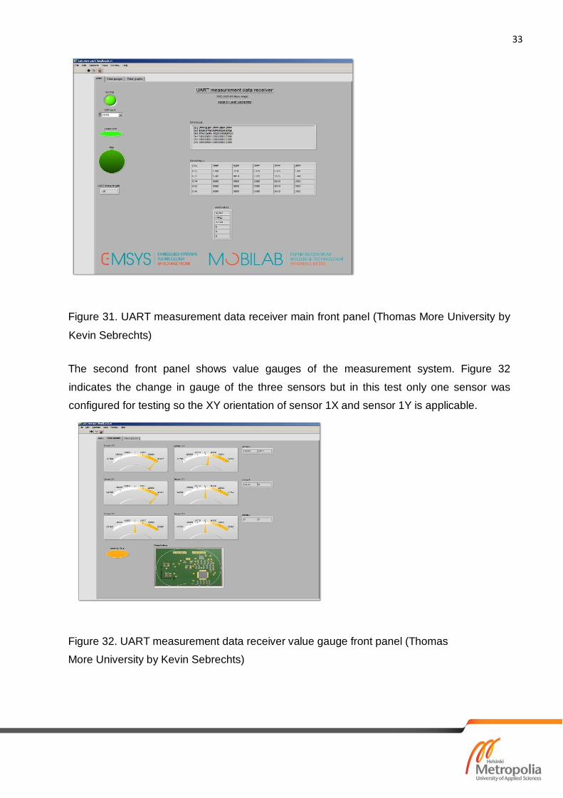
33
Figure 31. UART measurement data receiver main front panel (Thomas More University by
Kevin Sebrechts)
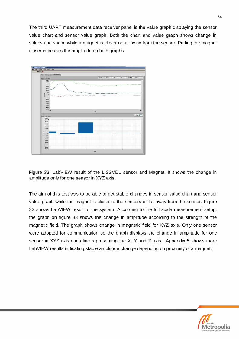
The second front panel shows value gauges of the measurement system. Figure 32
indicates the change in gauge of the three sensors but in this test only one sensor was
configured for testing so the XY orientation of sensor 1X and sensor 1Y is applicable.
Figure 32. UART measurement data receiver value gauge front panel (Thomas
More University by Kevin Sebrechts)
34
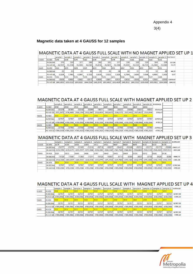
The third UART measurement data receiver panel is the value graph displaying the sensor
value chart and sensor value graph. Both the chart and value graph shows change in
values and shape while a magnet is closer or far away from the sensor. Putting the magnet
closer increases the amplitude on both graphs.
Figure 33. LabVIEW result of the LIS3MDL sensor and Magnet. It shows the change in
amplitude only for one sensor in XYZ axis.
The aim of this test was to be able to get stable changes in sensor value chart and sensor
value graph while the magnet is closer to the sensors or far away from the sensor. Figure
33 shows LabVIEW result of the system. According to the full scale measurement setup,
the graph on figure 33 shows the change in amplitude according to the strength of the
magnetic field. The graph shows change in magnetic field for XYZ axis. Only one sensor
were adopted for communication so the graph displays the change in amplitude for one
sensor in XYZ axis each line representing the X, Y and Z axis. Appendix 5 shows more
LabVIEW results indicating stable amplitude change depending on proximity of a magnet.

35
6.3 MCP2200 (USB 2.0 to UART Protocol Converter with GPIO)
The MCP2200 is a USB to UART converter with GPIO that enables closer study of
electronics projects and other applications. The UART interface has TX (Transmitter) and
Receiver (RX) data signals to be connected to RX and TX of the device under test. The
UART in this project was configured for 9600 baud rate and Real Term was used to display
the data in hexadecimal data format.
The ready-made MCP2200 board from Thomas More University has Vcc, GND, RX and TX
pin to connect to the microcontroller for proper data transmission and testing. The
measurement test was performed in different Gauss level for LIS3MDL with given gain at
16-bit.
Refer to table 1 under LIS3MDL digital output magnetic sensor subsection to see different
Gauss level for 16-bit. 4 gauss, 12 gauss and 16 gauss levels were selected under four
different setups with and without magnet to study this measurement. The calculation of the
milligauss and average gauss level were performed by changing the measured
hexadecimal data to decimal data format and following the specific gain level and dividing
by 1000 for milligauss level.
milliGauss = (Sample value in decimal) ÷ (gain value for specific fullscale×1000)
(2)
Averagegauss = (Addition of sample values in milligauss) ÷ (number of samples)
(3)
6.3.1 Real Term
Real term is a serial terminal designed to capture, control, debug and display output data in
binary or other complex data formats. It supports various configurations like SPI, I2C, 1Wire
chip control and others. The setting can be adjusted to users need and data can be
displayed in any of the formats listed on figure 34 below in Display As dialog box.
The baud rate relays on specific hardware ports. Once data is captured it is possible to
save it as hexadecimal data format. Adding the timestamp and delimiter will give received
data separated in time and comma or space depending on user selection.

36
Figure 34: Display Format of Real Term (Copied from Real Term Sourceforge
[24]).
Real term was used in testing LIS3MDL sensor so that it is possible to study the
performance of the sensor and the magnet. The distance between the sensor and the
magnet was measured to see the difference in the gauss level. Using Real Term, the
displayed hexadecimal data used to calculate the magnetic field in gauss. Appendix 4 page
one and two shows the four different magnet position setups used to measure the sensor
performance. The results of the sensor was logged in excel as shown in appendix 4 of page
3 to be able to calculate the sample results in decimal data format and milligauss based on
formula 2 . Note that, the result from the Real Term is in hexadecimal format.
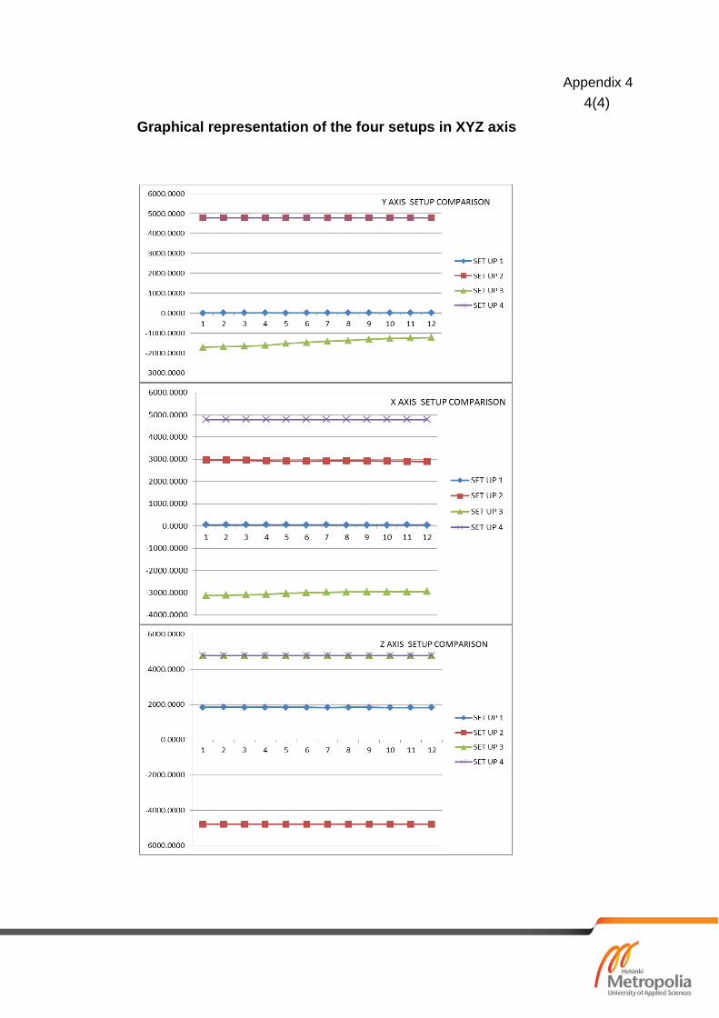
The average gauss can be calculated using formula 3 for XYZ axis. Using excel the result
data was also shown in graphical representation as shown in the last page of appendix 4.
Depending on the datasheet of LIS3MDl sensor the sensitivity describes the gain of the
sensor which can be determined by applying a magnet field of a specific gauss to the
sensor. Considering page 3 of appendix 4, the XYZ axis of the sensor without magnet
shows deviation of an output signal from the ideal output and setup 2, 3 and 4 with magnet
applied at 4 gauss shows an overflow due to gauss level over 4000 miligauss.

37
7 Conclusion and Discussion
The thesis explains the development of knee angle measurement consisting of various
systems; sensors, analog front end, microcontroller and wireless module. Various
development tools and software has been used while working on knee angle measurement
for example LabVIEW, code composer studio, saleae logic analyzer, real term, excel,
MCP2200 configuration utility, oscilloscope and other applications. Due to unknown reason,
this electrical connection was not able to operate properly even though the soldering of the
external capacitors was done twice for checking. As a result, LIS3MDL adapter board
(STEVAL-MKI137V1) was replaced to solve the problem.
The ADS showed incomplete data functionality with the inability of proper ADS initialization.
Timing problem is the expected cause. The wireless module presented complete
performance of the chip. The RF antenna, the SPI configuration, receiver and timing
showed meaningful results.
The difficulties in designed schematics and PCB board were solved by swapping and
rearranging specific ports. The system can be improved by replacing CC430, an ultra-low
power microcontroller system with integrated RF module. Moreover, eliminating the ADS to
save up power consumption and reduce the printed circuit board will add up more
advantages to the system.
It can be concluded that the aim of the project was met in presenting the readable and
descriptive code flow, upgrading the system to LIS3MDL sensors for better performance
and most importantly, presenting stable output data and channel depending on the position
and distance of the magnet.

References
1 DR. RICHARD P.B.VON BORMANN. [Online].
http://www.capetownkneesurgery.co.za/knee-surgery-cape-town.php [Accessed 25 July 2015]
2 “Tomi's Physio therapy Blog”, Knee Injuries [Online]. http://thomasbondphysio.blogspot.fi/2014_09_02_archive.html
[Accessed 10 August 2015]
3 AESCULAP, Implants Systems, Type of Knee Implants, Knee Design.
[Online]. https://www.soactivesofast.com/knee/types-of-knee-implants. [Accessed 10 August 2015]
4 Knee Angle Measurement thesis documentation by Kevin Sebrechts and Sven Sleeckx, Thomas More University.
5 Arash ARAMI, Kinematics Estimation and Loosening Detection in Smart Knee Prostheses; Suisse 2014
6 A.Arami, A.Vallet and K.Aminian.Accurate Measurement of Concurrent Flexion-Extension and Internal External Rotations in Smart Knee Prostheses, in IEEE Transactions on Biomedical Engineering (TBME), 2013
7 Arash Arami, Hooman Dejnabadi, Vincent Leclercq and Kamiar Aminian. An Implantable System for Angles Measurement in Prosthetic Knee. International Society of Biomechanics (ISB), Brussels, Belgium 2011.
8 Chronic diseases and health promotion. [Online].
http://www.who.int/chp/topics/rheumatic/en/ [Accessed 10 August 2015]
9 A.Arami, M.Simonici, O.Atasoy, W.Hasenkamp and S.Ali et al. Instrumented Knee Prosthesis for Force and Kinematics Measurements, in IEEE Transactions on Automation Science and Engineering, 2013.
10 "supermagnete", S-05-08-N , Rod magnet.[Online]
http://www.supermagnete.de/eng/rod-magnets-neodymium/rod-magnetdiameter- 5mm-height-8.47mm-neodymium-n45-nickel-plated_S-05-08-N. [Accessed 10 August 2015 ]
11 KOHDEN, Principle of the AMR sensor. [Online]. http://www.hkd.co.jp/english/amr_tec_amr/ [Accessed 13 August 2015]
12 "Honeywell" Magnetic Displacement Sensors, HMC1501/1512 datasheet. [Online.] http://www.farnell.com/datasheets/1681861.pdf. [Accessed 20 August 2015]

13 STMicroelectronics, LIS3MDL datasheet-production data. [Online]. http://www.st.com/st-
webui/static/active/en/resource/technical/document/datasheet/DM00075867.pdf [Accessed 20 August 2015]
14 STMicroelectronics, LIS3MDL Application Note. [Online].
http://www.st.com/st-webui/static/active/cn/resource/technical/document/application_note/DM0013662 6.pdf. [Accessed 20 August 2015]
15 STMelectronics,STEVAL-MKI137V1 LIS3MDL adapter board for standard DIL24 socket datasheet.[Online]
http://www.st.com/st-webui/static/active/en/resource/technical/document/data_brief/DM00089855.pdf.[Accessed 22 August 2015]
16 STARS; Sensors Technology Applied In Reconfigurable Systems; Analog Front Ends. [Online].
http://starsproject.nl/activities/theme2/ [Accessed 13 August 2015]
17 "Texas Instruments", ADS1296 Analog to Digital Converter with Integrated ECG Front End. [Online].
http://www.ti.com/lit/ds/symlink/ads1296.pdf [Accessed 13 August 2015]
18 "Texas Instruments", SLAU272; MSP430FR57xx Family User Guide.
[Online]. http://www.ti.com/lit/ug/slau272c/slau272c.pdf. [Accessed 17 August 2015]
19 "Texas Instruments", MSP-FET430UIF universal programmer, MSP430 hardware tool.
http://www.ti.com/lit/ug/slau278v/slau278v.pdf. [Accessed 17 August 2015]
20 "Nordic Semiconductors", nRF24L01 product specification. [Online]. http://www.nordicsemi.com/eng/Products/2.4GHz-RF/nRF24L01.[Accessed
20 August 2015]
21 Saleae Logic Analyzer. [Online].
https://www.saleae.com/index.[Accessed 20 August 2015]
22 "Microchip", MCP2200 USB 2.0 to UART Protocol Converter with GPIO.
[Online]. http://ww1.microchip.com/downloads/en/DeviceDoc/22228B.pdf.[Accessed
20 August 2015]
23 Realterm: Serial Terminal.[Online].
http://realterm.sourceforge.net/ [Accessed 08 September 2015]

Appendix 1
1(1)
Measurement Setup including Transmitter and Receiver

Appendix 2
1(1)
QFN Package design for the Microcontroller (Created by Kevin Sabrechts, Thomas
More University)

Appendix 3
1(1)
Saleae Logic Analyzer test results

Appendix 4
1(4)
Four different magnet position setups

Appendix 4
Four different magnet position setups 2(4)
Appendix 4
3(4)
Magnetic data taken at 4 GAUSS for 12 samples
Appendix 4
4(4)
Graphical representation of the four setups in XYZ axis
Appendix 5
1(1)
Test result of the system from LabVIEW