Embed Size (px)
Citation preview

Kingston Technology Secure Digital™ High Capacity - Micro Series
Digital Storage Cards 1. Introduction The High Capacity microSD memory card is functionally compatible with the SD memory specification but is smaller in dimension. This microSD memory card can also be inserted into a microSD memory card adapter and used as a standard Secure Digital memory card.
2. Part Number(s) • SDC4/4GB
• SDC4/8GB
3. SD Card Features
Table 1: SDHC Card Features Design Standard
Contents None (OEM Design Available)
Security Functions SD Security Specification Ver.2.00 Compliant (CPRM Based) *CPRM: Contents Protection for Recording Media Specification
Logical Format SD Files System Specification Ver.2.00 Compliant (DOS-FAT Based formatted)
ID, MKB Programmed
Electrical Operating Voltage: 2.7V to 3.6V (Memory Operation) Interfaces: SD Card Interface, (SD : 4 or 1bit) SPI Mode Compatible SD Physical Layer Specification Ver.2.00 Compliant
Physical L: 15, W: 11 , T: 1.0 (mm), Weight: 0.5g (typ.) microSD Memory Card Specification Ver. 1.00 Compliant (Detailed Dimensions included at: Appendix .1)
Durability SD Physical Layer Specification Ver.2.00 Compliant microSD Memory Card Specification Ver. 1.00 Compliant
ROHS ROHS Compatible.
Document No: 4808027-001.B01
08/29/2008

T
4. Compatibility Compliant Specifications
SD Memory Card Specifications • Compliant with PHYSICAL LAYER SPECIFICATION Ver.2.00. (Part1) • Compliant with FILE SYSTEM SPECIFICATION Ver.2.00. (Part2) • Compliant with SECURITY SPECIFICATION Ver.2.00. (Part3) • microSD Memory Card Specification Ver.1.00
Supplementary Explanation are described in “8.Others: Limited Conditions, SD Specification Compliance” in this document. 5. Physical Characteristics 5.1. Environmental Characteristics 1) Operation Conditions
Temperature Range: Ta = -25° to +85° C
2) Storage Conditions
Temperature Range: Tstg = -40° to +85° C
5.2. Physical Characteristics 1) Hot Insertion or Removal Kingston microSD Card can be removed and/ or inserted without powering off the host system. 2) Mechanical Write Protect Switch microSD memory Card has no mechanical write protect switch.
2

7
T
Table.4: SPI Mode Command set
(+: Implemented, -: Not Implemented) CMD Index Abbreviation Implementa
tion Note
CMD0 GO_IDLE_STATE + CMD1 SEND_OP_CND + NOTICE: DO NOT USE (SEE Fig.6 and 9.2 ) CMD9 SEND_CSD + CMD10 SEND_CID + CMD12 STOP_TRANSMISSION + CMD13 SEND_STATUS + CMD16 SET_BLOCKLEN + CMD17 READ_SINGLE_BLOCK + CMD18 READ_MULTIPLE_BLOCK + CMD24 WRITE_BLOCK + CMD25 WRITE_MULTIPLE_BLOCK + CMD27 PROGRAM_CSD + CMD28 SET_WRITE_PROT - Internal Write Protection is not implemented. CMD29 CLR_WRITE_PROT - Internal Write Protection is not implemented. CMD30 SEND_WRITE_PROT - Internal Write Protection is not implemented. CMD32 ERASE_WR_BLK_START_ADDR + CMD33 ERASE_WR_BLK_END_ADDR + CMD38 ERASE + CMD42 LOCK_UNLOCK + . CMD55 APP_CMD + CMD56 GEN_CMD - This command is not specified . CMD58 READ_OCR + CMD59 CRC_ON_OFF + ACMD6 SET_BUS_WIDTH + ACMD13 SD_STATUS + ACMD22 SEND_NUM_WR_BLOCKS + ACMD23 SET_WR_BLK_ERASE_COUNT + ACMD41 SD_APP_OP_COND + ACMD42 SET_CLR_CARD_DETECT + ACMD51 SEND_SCR + ACMD18 SECURE_READ_MULTI_BLOCK + ACMD25 SECURE_WRITE_MULTI_BLOCK + ACMD26 SECURE_WRITE_MKB + ACMD38 SECURE_ERASE + ACMD43 GET_MKB + ACMD44 GET_MID + ACMD45 SET_CER_RN1 + ACMD46 SET_CER_RN2 + ACMD47 SET_CER_RES2 + ACMD48 SET_CER_RES1 + ACMD49 CHANGE_SECURE_AREA +
CMD28,29,30 and CMD42 are Optional Commends. CMD56 is for vender specific command. Which is not defined in the standard card.
3

7
6.2 microSD Card Bus Topology
The microSD Memory Card supports two alternative communication protocols: SD and SPI Bus Mode.
Host System can choose either one of modes. Same Data of the microSD Card can read and write by both modes.
SD Mode allows the 4-bit high performance data transfer. SPI Mode allows easy and common interface for SPI channel. The disadvantage of this mode is loss of performance, relatively to the SD mode.
6.2.1 SD Bus Mode protocol
The SD bus allows the dynamic configuration of the number of data line from 1 to 4 Bi-directional data signal. After power up by default, the microSD card will use only DAT0. After initialization, host can change the bus width.
Multiplied microSD cards connections are available to the host. Common Vdd, Vss and CLK signal connections are available in the multiple connection. However, Command, Respond and Data lined (DAT0-DAT3) shall be divided for each card from host. This feature allows easy trade off between hardware cost and system performance. Communication over the microSD bus is based on command and data bit stream initiated by a start bit and terminated by stop bit. Command: Commands are transferred serially on the CMD line. A command is a token to starts an operation from host to the card. Commands are sent to a addressed single card(addressed Command) or to all connected cards (Broad cast command). Response: Responses are transferred serially on the CMD line. A response is a token to answer to a previous received command. Responses are sent from a addressed single card or from all connected cards. Data: Data can be transfer from the card to the host or vice versa. Data is transferred via the data lines.
Fig 4: microSD Card (SD Mode) connection Diagram CLK : Host card Clock signal CMD : Bi-directional Command/ Response Signal DAT0 - DAT3 : 4 Bi-directional data signal Vdd : Power supply Vss : GND
microSD
microSD
4

T
Table 3.:SD Mode Command Set
(+: Implemented, -: Not Implemented)
CMD Index Abbreviation Implementation
Note
CMD0 GO_IDLE_STATE + CMD2 ALL_SEND_CID + CMD3 SEND_RELATIVE_ADDR + CMD4 SET_DSR - DSR Register is not implemented. CMD7 SELECT/DESELECT_CARD + CMD9 SEND_CSD + CMD10 SEND_CID + CMD12 STOP_TRANSMISSION + CMD13 SEND_STATUS + CMD15 GO_INACTIVE_STATE + CMD16 SET_BLOCKLEN + CMD17 READ_SINGLE_BLOCK + CMD18 READ_MULTIPLE_BLOCK + CMD24 WRITE_BLOCK + CMD25 WRITE_MULTIPLE_BLOCK + CMD27 PROGRAM_CSD + CMD28 SET_WRITE_PROT - Internal Write Protection is not implemented. CMD29 CLR_WRITE_PROT - Internal Write Protection is not implemented. CMD30 SEND_WRITE_PROT - Internal Write Protection is not implemented. CMD32 ERASE_WR_BLK_START + CMD33 ERASE_WR_BLK_END + CMD38 ERASE + CMD42 LOCK_UNLOCK + . CMD55 APP_CMD + CMD56 GEN_CMD - This command is not specified . ACMD6 SET_BUS_WIDTH + ACMD13 SD_STATUS + ACMD22 SEND_NUM_WR_BLOCKS + ACMD23 SET_WR_BLK_ERASE_COUNT + ACMD41 SD_APP_OP_COND + ACMD42 SET_CLR_CARD_DETECT + ACMD51 SEND_SCR + ACMD18 SECURE_READ_MULTI_BLOCK + ACMD25 SECURE_WRITE_MULTI_BLOCK + ACMD26 SECURE_WRITE_MKB + ACMD38 SECURE_ERASE + ACMD43 GET_MKB + ACMD44 GET_MID + ACMD45 SET_CER_RN1 + ACMD46 SET_CER_RN2 + ACMD47 SET_CER_RES2 + ACMD48 SET_CER_RES1 + ACMD49 CHANGE_SECURE_AREA +
CMD28,29,30 and CMD42 are Optional Commands. CMD4 is not implemented because DSR register (Optional Register) is not implemented. CMD56 is for vender specific command. Which is not defined in the standard card.
5

T
6.2.2 SPI Bus mode Protocol
The SPI bus allows 1 bit Data line by 2-chanel (Data In and Out).
The SPI compatible mode allows the MMC Host systems to use SD card with little change. The SPI bus mode protocol is byte transfers.
All the data token are multiples of the bytes (8-bit) and always byte aligned to the CS signal.
The advantage of the SPI mode is reducing the host design in effort.
Especially, MMC host can be modified with little change.
The disadvantage of the SPI mode is the loss of performance versus SD mode.
Caution: Please use SD Card Specification. DO NOT use MMC Specification.
For example, initialization is achieved by ACMD41, and be careful to Register. Register definition is different, especially CSD Register.
Fig 5: microSD card (SPI mode) connection diagram CS : Card Select Signal CLK : Host card Clock signal Data in : Host to card data line Data out : card to host data line Vdd : Power supply Vss : GND
microSD
microSD
6
7
T
Table.4: SPI Mode Command set
(+: Implemented, -: Not Implemented) CMD Index Abbreviation Implementa
tion Note
CMD0 GO_IDLE_STATE + CMD1 SEND_OP_CND + NOTICE: DO NOT USE (SEE Fig.6 and 9.2 ) CMD9 SEND_CSD + CMD10 SEND_CID + CMD12 STOP_TRANSMISSION + CMD13 SEND_STATUS + CMD16 SET_BLOCKLEN + CMD17 READ_SINGLE_BLOCK + CMD18 READ_MULTIPLE_BLOCK + CMD24 WRITE_BLOCK + CMD25 WRITE_MULTIPLE_BLOCK + CMD27 PROGRAM_CSD + CMD28 SET_WRITE_PROT - Internal Write Protection is not implemented. CMD29 CLR_WRITE_PROT - Internal Write Protection is not implemented. CMD30 SEND_WRITE_PROT - Internal Write Protection is not implemented. CMD32 ERASE_WR_BLK_START_ADDR + CMD33 ERASE_WR_BLK_END_ADDR + CMD38 ERASE + CMD42 LOCK_UNLOCK + . CMD55 APP_CMD + CMD56 GEN_CMD - This command is not specified . CMD58 READ_OCR + CMD59 CRC_ON_OFF + ACMD6 SET_BUS_WIDTH + ACMD13 SD_STATUS + ACMD22 SEND_NUM_WR_BLOCKS + ACMD23 SET_WR_BLK_ERASE_COUNT + ACMD41 SD_APP_OP_COND + ACMD42 SET_CLR_CARD_DETECT + ACMD51 SEND_SCR + ACMD18 SECURE_READ_MULTI_BLOCK + ACMD25 SECURE_WRITE_MULTI_BLOCK + ACMD26 SECURE_WRITE_MKB + ACMD38 SECURE_ERASE + ACMD43 GET_MKB + ACMD44 GET_MID + ACMD45 SET_CER_RN1 + ACMD46 SET_CER_RN2 + ACMD47 SET_CER_RES2 + ACMD48 SET_CER_RES1 + ACMD49 CHANGE_SECURE_AREA +
CMD28,29,30 and CMD42 are Optional Commends. CMD56 is for vender specific command. Which is not defined in the standard card.
7

6.3. microSD Card Initialize
To initialize the Toshiba microSD card, follow the following procedure is recommended example.
1) Supply Voltage for initialization.
Host System can apply the Operating Voltage from initialization to the card.
Apply more than 74 cycles of Dummy-clock to the microSD card.
2) Select operation mode (SD mode or SPI mode)
In case of SPI mode operation, host should drive 1 pin(CD/DAT3) of SD Card I/F to “Low” level. Then, issue CMD0.
In case of SD mode operation, host should drive or detect 1 pin of microSD Card I/F (Pull up register of 1 pin is pull
up to “High” normally).
Card maintain selected operation mode except re-issue of CMD0 or power on below is SD mode initialization procedure.
3) Send the ACMD41 with Arg = 0 and identify the operating voltage range of the miniCard. 4) Apply the indicated operating voltage to the card.
Reissue ACMD41 with apply voltage storing and repeat ACMD41 until the busy bit is cleared.
(Bit 31 Busy = 1) If response time out occurred, host can recognize not microSD Card.
Note: In MMC-SPI Mode, CMD1 can use in this state. However, do not use CMD1 in case of SD Mode.
5) Issue the CMD2 and get the Card ID (CID).
Issue the CMD3 and get the RCA. (RCA value is randomly changed by access, not equal zero)
6) Issue the CMD7 and move to the transfer state.
If necessary, Host may issue the ACMD42 and disabled the pull up resistor for Card detect.
7) Issue the ACMD13 and poll the Card status as SD Memory Card. Check SD_CARD_TYPE value. If significant 8 bits are “all zero”, that means SD Card. If it is not, stop initialization.
8) Issue CMD7 and move to standby state.
Issue CMD9 and get CSD.
Issue CMD10 and get CID.
9) Back to the Transfer state with CMD7.
Issue ACMD6 and choose the appropriate bus-width.
Then the Host can access the Data between the microSD card as a storage device.
8

ACMD41with HCS=0
No response
Power-on
CMD0
Ver2.00 or laterSD Memory Card
CMD8
Non- compatible voltage rangeor check pattern is not correct
Ver2.00 or later SD Memory Card(voltage mismatch)or Ver1.X SD Memory Card
or not SD Memory Card
Compatible voltage rangeand check pattern is correct
ACMD41with HCS=0or1
Card returns response
ValidResponse?
Card with compatibleVoltage range
Card isready?
Card returnsbusy
cards with non compatible voltage rangeor time- out(no response or busy) occurs
Card isready?
cards with non compatiblevoltage range(card goes to
'ina' state) or time-out(no response or busy) occurs
UnusableCard
UnusableCard
UnusableCard
Card returnsbusy
Card returnsready
Ver1.XStandard CapacitySD Memory Card
CCS inResponse?
Card returns ready
Ver2.00 or laterStandard CapacitySD Memory Card
Ver2.00 or laterHigh Capacity
SD Memory Card
CCS=0
CCS=1
Not SD Memory Card
No response
CMD2
CMD3
If host supports high capacity, HCS is set to 1
Get CID
Get RCA
* to Fig6-2
Fig 6-1. microSD card Initialize Procedure
9

Fig 6-2. microSD card Initialize Procedure
CMD9
CMD7
Choose Data Bus Width
Choose card with RCA
* from Fig.6-1
Transfer mode Data Access Enabled
ACMD42
Get SD status
YES
CMD7
CMD10
CMD7
Get CSD
Choose card with RCA
Idle state with RCA=0000
Get CID
ACMD6
Other SD card (SD IO or Others)
ACMD3
Disable the Pull-up Resister (If necessary)
MemoryCard
No
10
2008/01/21 14/63 TOSHIBA CONFIDENTIAL
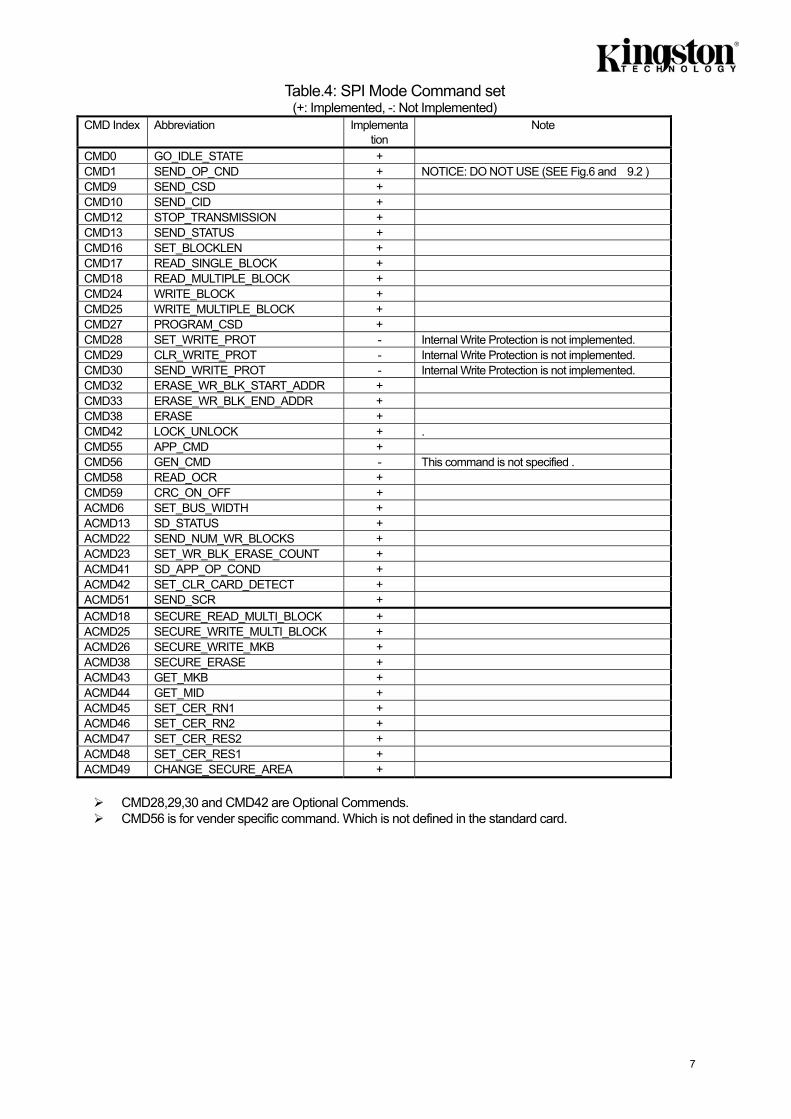
6.3.2 DC Characteristics
Table 6: DC Characteristics Item Symbol Condition MIN. Typ. MAX. Unit Note
Supply Voltage - 2.7 - 3.6 V High Level VIH - VDD*0.625 - - V Input
Voltage Low Level VIL - - - VDD*0.25 V
High Level VOH VDD = 2V IOH = -100uA VDD*0.75 - - V
Output Voltage Low Level VOL
VDD = 2V IOL = 100uA
- - VDD*0.125 V
3.6V Clock 25MHz - - 30 @25 deg
Standby Current ICC1 3.0V Clock Stop - - 0.55
mA @25 deg
- - 150 Write Operation Current *) ICC2 3.6V/25MHz,
50MHz - - 150 mA Read Input Voltage Setup
Time Vrs - - - 250 ms
*) Peak Current: RMS value over a 10 usec period Table 7: Signal Capacitance
Item Symbol Min. Max. Unit Note
Pull up Resistance RCMD RDAT
10 100 K Ohm
Bus Signal Line Capacitance CL - 250 pF FPP<5MHz
(21Cards) Bus Signal Line Capacitance CL - 100 pF FPP<20MHz
(7Cards) Single Card Capacitance CCARD - 10 pF
Pull up Resistance inside card(pin1) RDAT3 10 90 K Ohm
Note: WP pull-up (Rwp) Value is depend on the Host Interface drive circuit.
11

7
T
6.3.3 AC Characteristics
^
FPP
TWL TWH
TTHL TTLH
TISU TIH
TODLY TODLY(MAX) (MIN)
CLK
INPUT
OUTPUT
VIH
VIH
VOH
VOL
VIL
VIL
Fig 7: AC Timing Diagram
Table 8: AC Characteristics
Item Symbol Min. Max. Unit Note Clock Frequency (In any Sates) Fsty 0 25 MHz CL<100pF
(7Cards) Clock Frequency (Data transfer Mode) FPP 0.1 25 MHz CL<100pF
(7Cards) Clock Frequency (Card identification Mode) FOD 100 400 kHz CL<250pF
(21Cards) Clock Low Time TWL 10 - ns Clock High Time TWH 10 - ns Clock Rise Time TTLH - 10 ns Clock Fall Time TTHL - 10 ns
CL<100pF (7Cards)
Clock Low Time TWL 50 - ns Clock High Time TWH 50 - ns Clock Rise Time TTLH - 50 ns Clock Fall Time TTHL - 50 ns
CL < 250pF (21Cards)
Input Setup Time TISU 5 - ns Input Hold Time TIH 5 - ns Output Delay Time TODLY 0 14 ns
CL < 25pF (1Cards)
12

7
T
7. Card Internal Information 7.1. Security Information MKB (Media Key Block) and Media ID are Standard Information. These informations are compliance with the CPRM. Note: The security information is NOT Development information for evaluation. Host System shall be compliance with the CPRM to use the security function. This information is kept as confidential because of security reasons. 7.2. microSD Card Registers The microSD card has six registers and SD Status information: OCR, CID, CSD, RCA, DSR, SCR and SD Status. DSR IS NOT SUPPORTED in this card. There are two types of register groups.
MMC compatible registers: OCR, CID, CSD, RCA, DSR, SCR
SD card Specific: SD Status
Table.9 : microSD card Registers Resister Name
Bit Width Description
OCR 32 Operation Conditions (VDU Voltage Profile and Busy Status Information) CID 128 Card Identification information CSD 128 Card specific information RCA 16 Relative Card Address DSR 16 Not Implemented (Programmable Card Driver): Driver Stage Register SCR 64 SD Memory Card’s special features
SD Status 512 Status bits and Card features
13

2008/01/21 18/63
7.2.1. OCR Register This 32-bit register describes operating voltage range and status bit in the power supply. (Refer Appendix 2. for the detail)
Table 10: OCR register definition Initial value OCR bit
position VDD voltage window
4GB 8GB 31 Card power up status
bit(busy) “0” = busy “1” = ready
30-24 reserved All ‘0’ 23 3.6 – 3.5 1 22 3.5 – 3.4 1 21 3.4 – 3.3 1 20 3.3 – 3.2 1 19 3.2 – 3.1 1 18 3.1 – 3.0 1 17 3.0 – 2.9 1 16 2.9 – 2.8 1 15 2.8 – 2.7 1 14 2.7 – 2.6 0 13 2.6 – 2.5 0 12 2.5 – 2.4 0 11 2.4 – 2.3 0 10 2.3 – 2.2 0 9 2.2 – 2.1 0 8 2.1 – 2.0 0 7 2.0 – 1.9 0 6 1.9 – 1.8 0 5 1.8 – 1.7 0 4 1.7 – 1.6 0 3-0 reserved All ‘0’
bit 23-4: Describes the microSD Card Voltage bit 31 indicates the card power up status. Value “1” is set after power up and initialization procedure has been completed.
14

2008/01/21 20/63 CONFIDENTIAL
7.2.2. CSD Register
CSD is Card-Specific Data register provides information on 128bit width. Some field of this register can writable by PROGRAM_CSD (CMD27).
Table.11: CSD Register
Initial Value Field Wid
th
Cell
Type(1)
CSD
slice
4GB 8GB
CSD_STRUCTURE 2 R [127:126] 01
- 6 R [125:120] All ‘0’ TAAC 8 R [119:112] 0_0001_110(1ms)
NSAC 8 R [111:104] 00000000
TRAN_SPEED 8 R [103:96] 0_0110_010(25Mbps)
CCC 12 R [95:84] 0_1_0_1_1_0_1_1_0_1_0_1
READ_BL_LEN 4 R [83:80] 1001 1001
READ_BL_PARTIAL 1 R [79:79] 0
WRITE_BLK_MISALIGN 1 R [78:78] 0
READ_BLK_MISALIGN 1 R [77:77] 0
DSR_IMP 1 R [76:76] 0
- 6 R [75:70] All ‘0’ C_SIZE 22 R [69:48] 0x1DFF 0x3BFF
- 1 R [47:47] 0
ERASE_BLK_EN 1 R [46:46] 1
SECTOR_SIZE 7 R [45:39] 11_1111_1
WP_GRP_SIZE 7 R [38:32] 000_0000
WP_GRP_ENABLE 1 R [31:31] 0
- 2 R [30:29] 00
R2W_FACTOR 3 R [28:26] 010
WRITE_BL_LEN 4 R [25:22] 1001
WRITE_BL_PARTIAL 1 R [21:21] 0
- 2 R [20:16] All ‘0’ FILE_FORMAT_GRP 1 R [15:15] 0
COPY 1 R/W(1) [14:14] 0
PERM_WRITE_PROTECT 1 R/W(1) [13:13] 0
TMP_WRITE_PROTECT 1 R/W [12:12] 0
FILE_FORMAT 2 R [11:10] 00
- 2 R [9:8] All ‘0’ CRC 7 R/W [7:1] (CRC)
- 1 - [0:0] 1
Cell Types: R: Read Only, R/W: Writable and Readable, R/W(1): One-time Writable / Readable Note: Erase of one data block is not allowed in this card. This information is indicated by “ERASE_BLK_EN”.
Host System should refer this value before one data block size erase.
15

7
T
・CSD_STRUCTURE
Version number of the related CSD structure.
Table 12-1:CSD_STRUCTURE
CSD_STRUCTURE CSD STRUCTURE VERSION
Valid for SD PHYSICAL LAYER SPECIFICATION Version
0 CSD Version 1.0 Version 1.0 1-3 Reserved
→ Version 1.0 Compliant ・TAAC Defines the asynchronous part of the data access time.
Table 12-2: TAAC Access Time Definition TAAC bit Code
2:0 Time Unit 0 = 1ns,1 = 10ns,2 = 100ns,3 = 1uS,4 = 10uS,5 = 100uS, 6 = 1ms,y = 10ms
6:3
Time Value 0 = Reserved,1 = 1.0,2 = 1.2,3 = 1.3,4 = 1.5,5 = 2.0, 6 = 2.5, 7 = 3.0,8 = 3.5,9 = 4.0,A = 4.5,B = 5.0,C = 5.5,D = 6.0, E = 7.0,F = 8.0
7 Reserved
→1ms ・NSAC Defines the worst case for the clock dependent factor of the data access time.
Unit is 100 clock cycle.
Total access time equal TAAC plus NSAC, calculation with actual clock frequency.
This is average delay by the first clock out put for data block.
→0 clock Cycle ・TRAN_SPEED The following table defines the maximum data transfer rate per one data line.
Table 12-3: Maximum Data Transfer Rate Definition TRAN_SPEED bit Code
2:0 Transfer Rate Unit 0 = 100kbit/s,1 = 1Mbit/s,2 = 10Mbit/s,3 = 100Mbit/s, 4-7 = Reserved
6:3
Time Value 0 = Reserved,1 = 1.0,2 = 1.2,3 = 1.3,4 = 1.5,5 = 2.0, 6 = 2.5, 7 = 3.0,8 = 3.5,9 = 4.0,A = 4.5,B = 5.0,C = 5.5,D = 6.0, E = 7.0,F = 8.0
7 Reserved → Trans Rate is 25Mbps
16

7
T
7. Card Internal Information 7.1. Security Information MKB (Media Key Block) and Media ID are Standard Information. These informations are compliance with the CPRM. Note: The security information is NOT Development information for evaluation. Host System shall be compliance with the CPRM to use the security function. This information is kept as confidential because of security reasons. 7.2. microSD Card Registers The microSD card has six registers and SD Status information: OCR, CID, CSD, RCA, DSR, SCR and SD Status. DSR IS NOT SUPPORTED in this card. There are two types of register groups.
MMC compatible registers: OCR, CID, CSD, RCA, DSR, SCR
SD card Specific: SD Status
Table.12-4 : microSD card Registers Resister Name
Bit Width Description
OCR 32 Operation Conditions (VDU Voltage Profile and Busy Status Information) CID 128 Card Identification information CSD 128 Card specific information RCA 16 Relative Card Address DSR 16 Not Implemented (Programmable Card Driver): Driver Stage Register SCR 64 SD Memory Card’s special features
SD Status 512 Status bits and Card features
17

7
T
・READ_BLK_MISALIGN Define whether the data block to be read by one command can be spread over more than one physical block of the Flash Memory Device.
Table 12-7:READ_BLK_MISALIGN
READ_BLK_MISALIGN Across Block Boundaries Read
0 Not Allowed 1 Allowed
→”0”: Invalid on this card
・DSR_IMP If set, a driver stage register (DSR) is implemented (supported).
Table 12-8 :DSR_IMP DSR_IMP DSR Type
0 DSR NOT Implemented 1 DSR Implemented
→“0”: DSR NOT implemented
・C_SIZE
This parameter is used to compute the user’s data card capacity(Not include the security area) as below.
Memory Capacity = BLOCKNR * BLOCK_LEN
BLOCKNR = (C_SIZE + 1) * MULT MULT = 2C_SIZ_MULT+2 (C_SIZE_MULT < 8) BLOCK_LEN = 2READ_BL_LEN (READ_BL_LEN < 12) Therefore the maximum capacity of the 64MB card is: 3784*32*512/1024/1024 = 59.125MB
→ The user’s data card capacity is as below. 512MB: 488.5MB 1GB: 982.5MB
・VDD_R_CURR_MIN,VDD_W_CURR_MIN The maximum values for Read/Write currents at VDD:MINIMUM.
Tab 12-9 VDD_R_CURR_MIN, VDD_W_CURR_MIN
VDD_R_CURR_MIN VDD_W_CURR_MIN
Code for current consumption @ VDU
2:0 0 = 0.5mA,1 = 1mA,2 = 5mA,3 = 10mA,4 =
25mA, 5 = 35mA,6 = 60mA,7 = 100mA
→60mA@Vdd = 2.7 V (Minimum)
18

7
T
・VDD_R_CURR_MAX,VDD_W_CURR_MAX The maximum values for Read/Write currents at VDD:MAXMUM.
Table 12-10:VDD_R_CURR_MAX,VDD_W_CURR_MAX VDD_R_CURR_MAX VDD_W_CURR_MAX R/W current Maximum
2:0 0 = 0.5mA,1 = 5mA,2 = 10mA,3 = 25mA,
4 = 35mA,5 = 45mA,6 = 80mA,7 = 200mA
→80mA @VDU = 3.6 V (Maximum) on this card
・C_SIZE_MULT
This parameter is used to compute the user’s data card capacity not include the security protected are refer to C_SIZE.
Table 12-11:Multiply Factor for the Device Size C_SIZE_MULT MULT
0 22 = 4 1 23 = 8 2 24 = 16 3 25 = 32 4 26 = 64 5 27 = 128 6 28 = 256 7 29 = 512
512MB : 28 =256, 1GB: 29 =512
・ERASE_BLK_EN (Caution!: This is different from MMC. Please be careful.)
WRITE_BL_LEN defines whether erase of one write block(see WRITE_BL_LEN) is allowed.
Table12-12:ERASE_BLK_EN ERASE_BLK_EN Description
0 Host cannot erase by WRITE_BL_LEN 1 Host can erase by WRITE_BL_LEN
→”1” : Can erase by WRITE_BL_LEN unit So should be check this value, and recognize how to erase.
19

7
T
・SECTOR_SIZE Sector defines the minimum erasable size. SECTOR_SIZE indicates the minimum erasable size as the number of write
blocks.
→ 1 Sector-size = 128 Write Blocks on this card ・WP_GRP_SIZE WP_GRP_SIZE defines the minimum number of sectors that can be set for the write protect group (WP_Group). A value of ’0’ means 1WP-Group = 1 erase sector,’127 means1WP-Group = 128 sectors.
→”1” : 1WP-Group is one sector on this card ・WP_GRP_ENABLE A value of “0” means not implemented (supported) the WP-Group functions.
Table12-13:WP_GRP_ENABLE WP_GRP_ENA
BLE Description
0 NOT Implemented 1 Implemented
→”0”: WP Group is not Implemented on this card
・R2W_FACTOR That is calculated R2W_FACTOR defines a multiple number for typical write time as a multiple of the read access time.
Table12-14:R2W_FACTOR R2W_FACTOR Multiples of read Access Time
0 1 1 2(Write half as fast as read) 2 4 3 8 4 16 5 32
6,7 Reserved
→”5”: Typical write time = Read Access timex32 on this card
20

7
T
・WRITE_BL_LEN The maximum write block length is calculated as 2WRITE_BL_LEN.
Table12-15:DATA Block Length WRITE_BL_LEN Block Length
0-8 Reserved 9 29 = 512Bytes ・・・ 11 211 = 2048Bytes
12-15 Reserved
→”9” :512Bytes on this card ・WRITE_BL_PARTIAL WRITE_BL_LEN defines whether partial block write is available.
Table12-16:Write Data size WRITE_BL_PARTIAL Block Oriented write Data size
0 Only the WRITE_BL_LEN size or 512Bytes are available 1 Partial size (Minimum 1Byte) write available
→”0”: Partial size write is not available on this card
・FILE_FORMAT_GRP/FILE_FORMAT Indicates the selected group of file format group and file format.
Table12-17:File Format FILE_FORMAT_GRP FILE_FORMAT Kinds
0 0 Hard disk-like File system with partition table 0 1 DOS FAT(floppy-like) with boot sector only
(No partition table) 0 2 Universal File Format 0 3 Others/Unknown 1 0,1,2,3 Reserved
Further information is given in SD Memory Card FILE SYSTEM SPECIFICATION.
→ [0.0] : Hard disk-like file system with partition table on this card
21

7
T
・COPY
Defines the contents of this card is original (=0) or duplicated (1). This bit is one time programmable.
Table12-18:COPY COPY Description
0 Original 1 Copy
→”0”: Original on this card
・PERM_WRITE_PROTECT
Permanently protects the whole card content against write or erase . This bit is one time programmable.
Table12-19:PERM_WRITE_PROTECT PERM_WRITE_PROTECT Description
0 Not protected/Writable 1 Permanently Write protected
→”0”: Not Protected/Writable on this card
・TMP_WRITE_PROTECT
Temporarily protects the whole card content against write or erase .
Table12-20:TMP_WRITE_PROTECT TMP_WRITE_PROTECT Description
0 Not protected/Writable 1 Temporarily Write Erase protected
→”0”: Not Protected/Writable on this card
・CRC
Calculated CRC for default data is set here. Host System is responsible to re-calculate this CRC if any CSD contents are changed.
22

2008/01/21 27/63 CONFIDENTIAL
7.2.4. RCA Register
The writable 16bit relative card address register carries the card address in SD Card mode. 7.2.5. DSR Register
This register is not implemented on this card 7.2.6. SCR Register SCR (SD Card Configuration Register) provides information on SD Memory Card’s special features.
The size of SCR Register is 64 bit. Table13: SCR Register
Value Field Width Cell Type
SCR Slice 4GB 8GB
SCR_STRUCTURE 4 R [63:60] 0000 SD_SPEC 4 R [59:56] 0010 DATA_STAT_AFTER_ERASE 1 R [55:55] 1 SD_SECURITY 3 R [54:52] 011 SD_BUS_WIDTHS 4 R [51:48] 0101 - 16 R [47:32] All ‘0’ - 32 R [31:0] Reserved for manufacture usage
・SCR_STRUCTURE Version number of the related structure in the SD Card PHYSICAL LAYER SPECIFICATION.
Table13-1: SCR_STRUCTURE SCR_STRUCTURE SCR STRUCTURE VERSION Valid for SD PHYSICAL LAYER SPECIFICATION
0 SCR Version 1.0 Version 1.0-2.00 1-15 Reserved
→”0”: Version 1.0 Compliant on this card
・SD_SPEC Describes the SD PHYSICAL LAYER SPECIFICATION version supported by this card.
Table13-2: SD_SPEC SD_SPEC SD PHYSICAL LAYER SPECIFICATION Version
0 Version 1.0-1.01 1 Version 1.10 2 Version2.00
3-15 Reserved
→“2” = Version2.00 Compliant on this card
23

7
T
7.2.6. SD Status
Table14:SD Status Value Identifier Width Type SD Status
Slice DAT_BUS_WIDTH 2 SR [511:510] 00 SECURED_MODE 1 SR [509] 0 - 13 - [508:496] All ‘0’ SD_CARD_TYPE 16 SR [495:480] 0x0000 SIZE_OF_PROTECTED_AREA 32 SR [479:448] 0x28 - 136 - [447:312] All ‘0’ - 312 - [311:0] All ‘0’
S: Status bit R: Set based on Command Response
・DAT_BUS_WIDTH Indicate the currently defined data bus width that was defined by SET_BUS_WIDTH command.
Table14-1:DAT_BUS_WIDTH DAT_BUS_WIDTH Bus Width
‘00’ 1 bit(default) ‘01’ Reserved ‘10’ 4 bit width ‘11’ Reserved
・SECURED_MODE Indicates whether card is in secure mode operation.
Table14-2:SECURED_MODE SECURED_MODE
Secured Mode Status
‘0’ NOT Secured Mode ‘1’ Secured Mode
・SD_CARD_TYPE
SD Card type described here.(Various SD types to be defined in the future.)
Table14-3:SD_CARD_TYPE SD_CARD_TYPE
SD Card Type
‘0000’h SD Memory Card
24

7 2828282523
T
Appendix 1. microSD Card Mechanical Dimensions (Unit : mm)
25