Embed Size (px)
Citation preview
Kinetis K66 Sub-Family180 MHz ARM® Cortex®-M4F Microcontroller.
The K66 sub-family members provide greater performance,memory options up to 2 MB total flash and 256 KB of SRAM, aswell as higher peripheral integration with features such as DualUSB and a 10/100 Mbit/s Ethernet MAC. These devices maintainhardware and software compatibility with the existing Kinetisfamily. This product also offers:
• Integration of a High Speed USB Physical Transceiver• Greater performance flexibility with a High Speed Run
mode• Smarter peripherals with operation in Stop modes
Performance• Up to 180 MHz ARM Cortex-M4 based core with DSP
instructions and Single Precision Floating Point unit
System and Clocks• Multiple low-power modes to provide power
optimization based on application requirements• Memory protection unit with multi-master protection• 3 to 32 MHz main crystal oscillator• 32 kHz low power crystal oscillator• 48 MHz internal reference
Security• Hardware random-number generator• Supports DES, AES, SHA accelerator (CAU)• Multiple levels of embedded flash security
Timers• Four Periodic interrupt timers• 16-bit low-power timer• Two 16-bit low-power timer PWM modules• Two 8-channel motor control/general purpose/PWM
timers• Two 2-ch quad decoder/general purpose timers• Real-time clock
Human-machine interface• Low-power hardware touch sensor interface (TSI)• General-purpose input/output
Memories and memory expansion• Up to 2 MB program flash memory on non-
FlexMemory devices with 256 KB RAM• Up to 1 MB program flash memory and 256 KB of
FlexNVM on FlexMemory devices• 4 KB FlexRAM on FlexMemory devices• FlexBus external bus interface and SDRAM controller
Analog modules• Two 16-bit SAR ADCs and two 12-bit DAC• Four analog comparators (CMP) containing a 6-bit
DAC and programmable reference input• Voltage reference 1.2V
Communication interfaces• Ethernet controller with MII and RMII interface to
external PHY and hardware IEEE 1588 capability• USB high-/full-/low-speed On-the-Go with on-chip
high speed transceiver• USB full-/low-speed OTG with on-chip transceiver• Two CAN, three SPI and four I2C modules• Low Power Universal Asynchronous Receiver/
Transmitter 0 (LPUART0) and five standard UARTs• Secure Digital Host Controller (SDHC)• I2S module
Operating Characteristics• Voltage/Flash write voltage range:1.71 to 3.6 V• Temperature range (ambient): -40 to 105°C
MK66FN2M0VMD18MK66FX1M0VMD18MK66FN2M0VLQ18MK66FX1M0VLQ18
144 MAPBGA (MD)13 mm x 13 mm Pitch 1
mm
144 LQFP (LQ)20 mm x 20 mm Pitch
0.5 mm
Freescale Semiconductor, Inc. K66P144M180SF5V2Data Sheet: Technical Data Rev. 3, 01/2016
© 2016 Freescale Semiconductor, Inc. All rights reserved.
Ordering Information 1
Part Number Memory Maximum number of I\O's
Flash SRAM
MK66FN2M0VMD18 2 MB 256 KB 100
MK66FX1M0VMD18 1.25 MB 256 KB 100
MK66FN2M0VLQ18 2 MB 256 KB 100
MK66FX1M0VLQ18 1.25 MB 256 KB 100
1. To confirm current availability of orderable part numbers, go to http://www.freescale.com and perform a part numbersearch.
Related Resources
Type Description Resource
SelectorGuide
The Freescale Solution Advisor is a web-based tool that featuresinteractive application wizards and a dynamic product selector.
Solution Advisor
ReferenceManual
The Reference Manual contains a comprehensive description of thestructure and function (operation) of a device.
K66P144M180SF5RMV21
Data Sheet The Data Sheet includes electrical characteristics and signalconnections.
This document.
Chip Errata The chip mask set Errata provides additional or corrective information fora particular device mask set.
Kinetis_K_0N65N 1
Packagedrawing
Package dimensions are provided in package drawings. MAPBGA 144-pin :98ASA00222D1
LQFP 144-pin: 98ASS23177W1
1. To find the associated resource, go to http://www.freescale.com and perform a search using this term.
2 Kinetis K66 Sub-Family, Rev.3, 01/2016.
Freescale Semiconductor, Inc.
Memories and Memory Interfaces
Programflash
RAM
12-bit DACx2
6-bit DACx4
CRC
interfacetouch-sensing
Programmable
Analog Timers Communication InterfacesSecurityand Integrity
SPIx3
Carriermodulatortransmitter
FlexMemory
Clocks
Frequency-
Core
Debuginterfaces
DSP
Interruptcontroller
comparatorx4
Analog
Voltagereference
SecureDigital
Low powertimer
Human-MachineInterface (HMI)
GPIO
System
protectionMemory
DMA
Internal
watchdogsand external
Low-leakagewakeup
locked loop
Serialprogramming
interface
Phase-locked loop
referenceInternal
clocks
delay block
timersinterruptPeriodic
Externalbus
real-timeIndependent
clock
oscillators
Low/highfrequency
UARTx5
Xtrinsic
® Cortex -M4ARM
Low powerTPM x 2 (4ch)
LPUART
SDRAM
®
Kinetis K66 Sub-Family
USB DCD/ USBHSDCD
USB voltageregulator
USB LS/FS OTG
controller with
transceiver
USB LS/FS/HSOTG
controllerwith
transceiver
x1I S2
Floating-point unit
controller
x4I C2Timers
x4 (20ch)
CANx2
IEEE 1588Timers
EthernetIEEE 1588
Hardwareencryption
numberRandom
generator
Cache
16-bit ADCx2
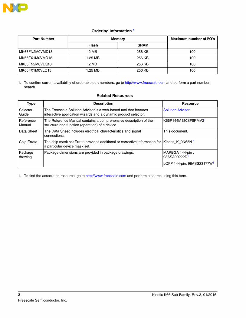
Figure 1. K66 Block Diagram
Kinetis K66 Sub-Family, Rev.3, 01/2016. 3
Freescale Semiconductor, Inc.
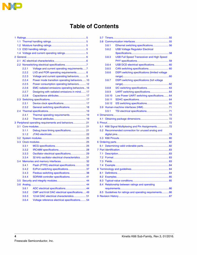
Table of Contents
1 Ratings....................................................................................5
1.1 Thermal handling ratings................................................. 5
1.2 Moisture handling ratings................................................ 5
1.3 ESD handling ratings.......................................................5
1.4 Voltage and current operating ratings............................. 5
2 General................................................................................... 6
2.1 AC electrical characteristics.............................................6
2.2 Nonswitching electrical specifications..............................7
2.2.1 Voltage and current operating requirements.....7
2.2.2 LVD and POR operating requirements............. 8
2.2.3 Voltage and current operating behaviors.......... 9
2.2.4 Power mode transition operating behaviors......10
2.2.5 Power consumption operating behaviors.......... 12
2.2.6 EMC radiated emissions operating behaviors...16
2.2.7 Designing with radiated emissions in mind....... 17
2.2.8 Capacitance attributes...................................... 17
2.3 Switching specifications...................................................17
2.3.1 Device clock specifications............................... 17
2.3.2 General switching specifications....................... 18
2.4 Thermal specifications.....................................................19
2.4.1 Thermal operating requirements....................... 19
2.4.2 Thermal attributes............................................. 19
3 Peripheral operating requirements and behaviors.................. 21
3.1 Core modules.................................................................. 21
3.1.1 Debug trace timing specifications..................... 21
3.1.2 JTAG electricals................................................ 22
3.2 System modules.............................................................. 25
3.3 Clock modules................................................................. 25
3.3.1 MCG specifications........................................... 25
3.3.2 IRC48M specifications...................................... 28
3.3.3 Oscillator electrical specifications..................... 29
3.3.4 32 kHz oscillator electrical characteristics.........31
3.4 Memories and memory interfaces................................... 32
3.4.1 Flash (FTFE) electrical specifications............... 32
3.4.2 EzPort switching specifications......................... 37
3.4.3 Flexbus switching specifications....................... 38
3.4.4 SDRAM controller specifications.......................41
3.5 Security and integrity modules........................................ 44
3.6 Analog............................................................................. 44
3.6.1 ADC electrical specifications.............................44
3.6.2 CMP and 6-bit DAC electrical specifications.....49
3.6.3 12-bit DAC electrical characteristics................. 51
3.6.4 Voltage reference electrical specifications........ 54
3.7 Timers..............................................................................55
3.8 Communication interfaces............................................... 55
3.8.1 Ethernet switching specifications...................... 56
3.8.2 USB Voltage Regulator Electrical
Specifications.................................................... 58
3.8.3 USB Full Speed Transceiver and High Speed
PHY specifications............................................ 59
3.8.4 USB DCD electrical specifications.................... 60
3.8.5 CAN switching specifications............................ 60
3.8.6 DSPI switching specifications (limited voltage
range)................................................................60
3.8.7 DSPI switching specifications (full voltage
range)................................................................62
3.8.8 I2C switching specifications.............................. 63
3.8.9 UART switching specifications.......................... 64
3.8.10 Low Power UART switching specifications....... 64
3.8.11 SDHC specifications......................................... 64
3.8.12 I2S switching specifications.............................. 65
3.9 Human-machine interfaces (HMI)....................................71
3.9.1 TSI electrical specifications...............................71
4 Dimensions............................................................................. 72
4.1 Obtaining package dimensions....................................... 72
5 Pinout......................................................................................72
5.1 K66 Signal Multiplexing and Pin Assignments.................72
5.2 Recommended connection for unused analog and
digital pins........................................................................79
5.3 K66 Pinouts..................................................................... 80
6 Ordering parts......................................................................... 82
6.1 Determining valid orderable parts....................................82
7 Part identification.....................................................................83
7.1 Description.......................................................................83
7.2 Format............................................................................. 83
7.3 Fields............................................................................... 83
7.4 Example...........................................................................84
8 Terminology and guidelines.................................................... 84
8.1 Definitions........................................................................84
8.2 Examples.........................................................................85
8.3 Typical-value conditions.................................................. 85
8.4 Relationship between ratings and operating
requirements....................................................................86
8.5 Guidelines for ratings and operating requirements..........86
9 Revision History...................................................................... 87
4 Kinetis K66 Sub-Family, Rev.3, 01/2016.
Freescale Semiconductor, Inc.
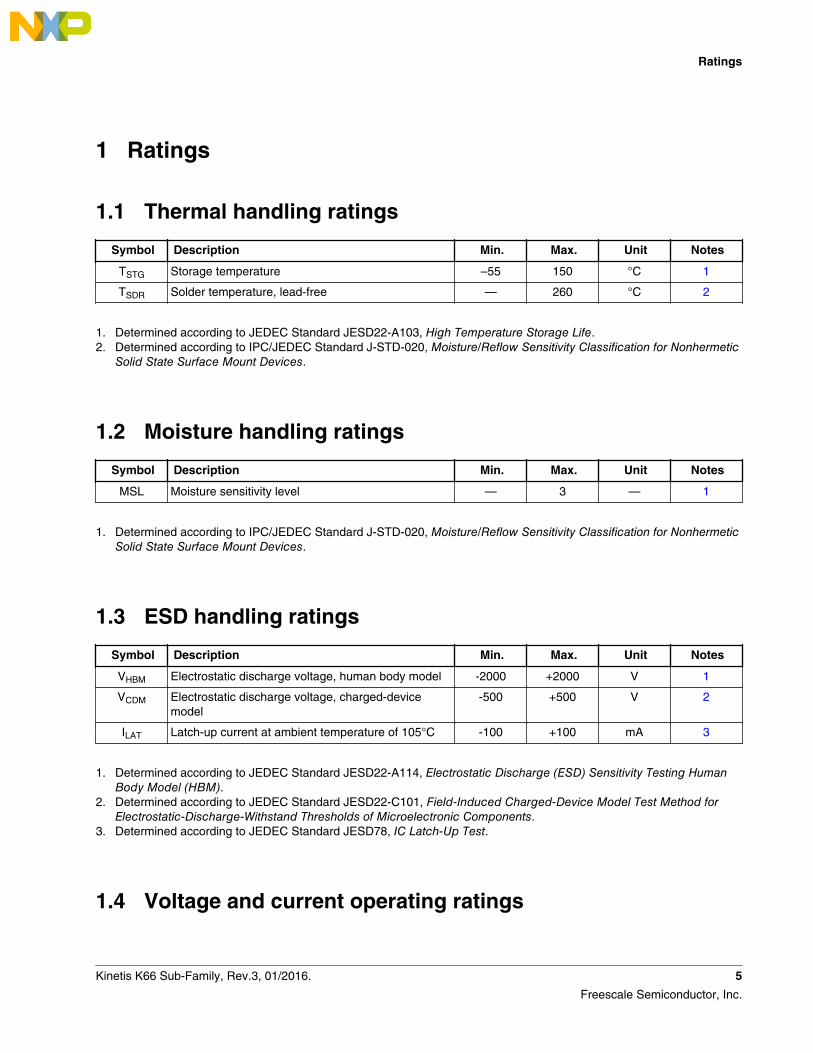
1 Ratings
1.1 Thermal handling ratings
Symbol Description Min. Max. Unit Notes
TSTG Storage temperature –55 150 °C 1
TSDR Solder temperature, lead-free — 260 °C 2
1. Determined according to JEDEC Standard JESD22-A103, High Temperature Storage Life.2. Determined according to IPC/JEDEC Standard J-STD-020, Moisture/Reflow Sensitivity Classification for Nonhermetic
Solid State Surface Mount Devices.
1.2 Moisture handling ratings
Symbol Description Min. Max. Unit Notes
MSL Moisture sensitivity level — 3 — 1
1. Determined according to IPC/JEDEC Standard J-STD-020, Moisture/Reflow Sensitivity Classification for NonhermeticSolid State Surface Mount Devices.
1.3 ESD handling ratings
Symbol Description Min. Max. Unit Notes
VHBM Electrostatic discharge voltage, human body model -2000 +2000 V 1
VCDM Electrostatic discharge voltage, charged-devicemodel
-500 +500 V 2
ILAT Latch-up current at ambient temperature of 105°C -100 +100 mA 3
1. Determined according to JEDEC Standard JESD22-A114, Electrostatic Discharge (ESD) Sensitivity Testing HumanBody Model (HBM).
2. Determined according to JEDEC Standard JESD22-C101, Field-Induced Charged-Device Model Test Method forElectrostatic-Discharge-Withstand Thresholds of Microelectronic Components.
3. Determined according to JEDEC Standard JESD78, IC Latch-Up Test.
1.4 Voltage and current operating ratings
Ratings
Kinetis K66 Sub-Family, Rev.3, 01/2016. 5
Freescale Semiconductor, Inc.
Symbol Description Min. Max. Unit
VDD Digital supply voltage –0.3 3.8 V
IDD Digital supply current — 300 mA
VDIO Digital1 input voltage,including RESET_b –0.3 VDD + 0.3 V
VAIO Analog1 input voltage, including EXTAL32 and XTAL32 –0.3 VDD + 0.3 V
ID Maximum current single pin limit (digital output pins) –25 25 mA
VDDA Analog supply voltage VDD – 0.3 VDD + 0.3 V
VUSB0_DP USB0_DP input voltage –0.3 3.63 V
VUSB1_DP USB1_DP input voltage –0.3 3.63 V
VUSB0_DM USB0_DM input voltage –0.3 3.63 V
VUSB1_DM USB1_DM input voltage –0.3 3.63 V
VUSB1_VBUS USB1_VBUS detect voltage –0.3 6.0 V
VREG_IN0,VREG_IN1
USB regulator input –0.3 6.0 V
VBAT RTC battery supply voltage –0.3 3.8 V
1. Digital pins have a general purpose I/O port assigned (e.g. PTA0). Analog pins do not have an associated generalpurpose I/O port.
2 General
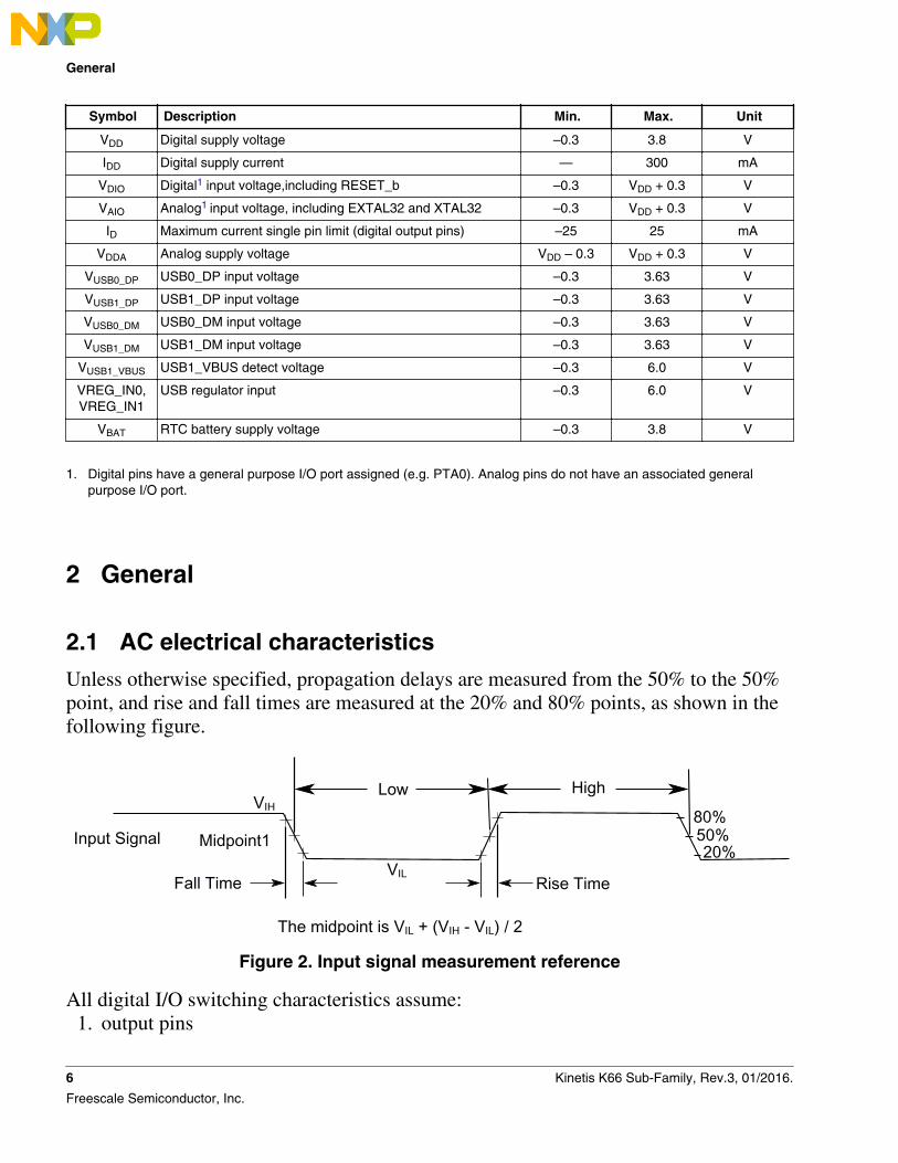
2.1 AC electrical characteristics
Unless otherwise specified, propagation delays are measured from the 50% to the 50%point, and rise and fall times are measured at the 20% and 80% points, as shown in thefollowing figure.
80%
20%50%
VIL
Input Signal
VIH
Fall Time
HighLow
Rise Time
Midpoint1
The midpoint is VIL + (VIH - VIL) / 2
Figure 2. Input signal measurement reference
All digital I/O switching characteristics assume:1. output pins
General
6 Kinetis K66 Sub-Family, Rev.3, 01/2016.
Freescale Semiconductor, Inc.
• have CL=30pF loads,• are slew rate disabled, and• are normal drive strength
2. input pins• have their passive filter disabled (PORTx_PCRn[PFE]=0)
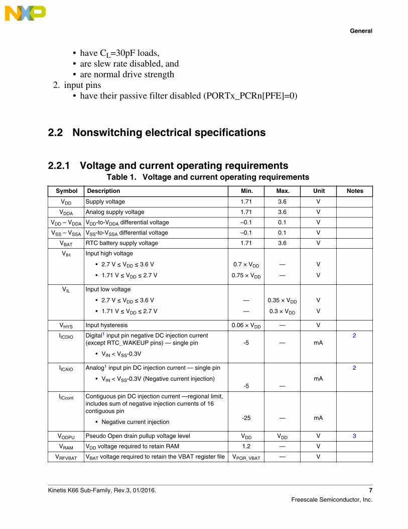
2.2 Nonswitching electrical specifications
2.2.1 Voltage and current operating requirementsTable 1. Voltage and current operating requirements
Symbol Description Min. Max. Unit Notes
VDD Supply voltage 1.71 3.6 V
VDDA Analog supply voltage 1.71 3.6 V
VDD – VDDA VDD-to-VDDA differential voltage –0.1 0.1 V
VSS – VSSA VSS-to-VSSA differential voltage –0.1 0.1 V
VBAT RTC battery supply voltage 1.71 3.6 V
VIH Input high voltage
• 2.7 V ≤ VDD ≤ 3.6 V
• 1.71 V ≤ VDD ≤ 2.7 V
0.7 × VDD
0.75 × VDD
—
—
V
V
VIL Input low voltage
• 2.7 V ≤ VDD ≤ 3.6 V
• 1.71 V ≤ VDD ≤ 2.7 V
—
—
0.35 × VDD
0.3 × VDD
V
V
VHYS Input hysteresis 0.06 × VDD — V
IICDIO Digital1 input pin negative DC injection current(except RTC_WAKEUP pins) — single pin
• VIN < VSS-0.3V
-5 — mA2
IICAIO Analog1 input pin DC injection current — single pin
• VIN < VSS-0.3V (Negative current injection)
-5
—mA
2
IICcont Contiguous pin DC injection current —regional limit,includes sum of negative injection currents of 16contiguous pin
• Negative current injection-25 — mA
VODPU Pseudo Open drain pullup voltage level VDD VDD V 3
VRAM VDD voltage required to retain RAM 1.2 — V
VRFVBAT VBAT voltage required to retain the VBAT register file VPOR_VBAT — V
General
Kinetis K66 Sub-Family, Rev.3, 01/2016. 7
Freescale Semiconductor, Inc.
1. Digital pins have a general purpose I/O port assigned (e.g. PTA0). Analog pins do not have an associated generalpurpose I/O port.
2. All digital and analog I/O pins are internally clamped to VSS through an ESD protection diode. There is no diodeconnection to VDD. If VIN is less than VSS-0.3V, a current limiting resistor is required. The minimum negative DCinjection current limiting resistor value is calculated as R=(-0.3-VIN)/|IICDIO| or R=(-0.3-VIN)/|IICAIO|. The actual resistorshould be an order of magnitude higher to tolerate transient voltages.
3. Open drain outputs must be pulled to VDD.
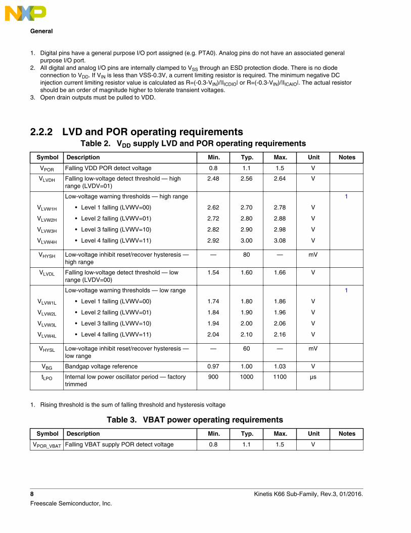
2.2.2 LVD and POR operating requirementsTable 2. VDD supply LVD and POR operating requirements
Symbol Description Min. Typ. Max. Unit Notes
VPOR Falling VDD POR detect voltage 0.8 1.1 1.5 V
VLVDH Falling low-voltage detect threshold — highrange (LVDV=01)
2.48 2.56 2.64 V
VLVW1H
VLVW2H
VLVW3H
VLVW4H
Low-voltage warning thresholds — high range
• Level 1 falling (LVWV=00)
• Level 2 falling (LVWV=01)
• Level 3 falling (LVWV=10)
• Level 4 falling (LVWV=11)
2.62
2.72
2.82
2.92
2.70
2.80
2.90
3.00
2.78
2.88
2.98
3.08
V
V
V
V
1
VHYSH Low-voltage inhibit reset/recover hysteresis —high range
— 80 — mV
VLVDL Falling low-voltage detect threshold — lowrange (LVDV=00)
1.54 1.60 1.66 V
VLVW1L
VLVW2L
VLVW3L
VLVW4L
Low-voltage warning thresholds — low range
• Level 1 falling (LVWV=00)
• Level 2 falling (LVWV=01)
• Level 3 falling (LVWV=10)
• Level 4 falling (LVWV=11)
1.74
1.84
1.94
2.04
1.80
1.90
2.00
2.10
1.86
1.96
2.06
2.16
V
V
V
V
1
VHYSL Low-voltage inhibit reset/recover hysteresis —low range
— 60 — mV
VBG Bandgap voltage reference 0.97 1.00 1.03 V
tLPO Internal low power oscillator period — factorytrimmed
900 1000 1100 μs
1. Rising threshold is the sum of falling threshold and hysteresis voltage
Table 3. VBAT power operating requirements
Symbol Description Min. Typ. Max. Unit Notes
VPOR_VBAT Falling VBAT supply POR detect voltage 0.8 1.1 1.5 V
General
8 Kinetis K66 Sub-Family, Rev.3, 01/2016.
Freescale Semiconductor, Inc.
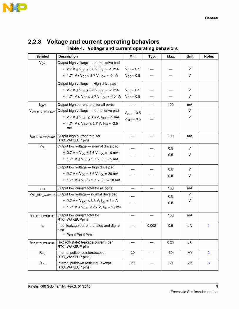
2.2.3 Voltage and current operating behaviorsTable 4. Voltage and current operating behaviors
Symbol Description Min. Typ. Max. Unit Notes
VOH Output high voltage — normal drive pad
• 2.7 V ≤ VDD ≤ 3.6 V, IOH = -10mA
• 1.71 V ≤VDD ≤ 2.7 V, IOH = -5mA
VDD – 0.5
VDD – 0.5
—
—
—
—
V
V
Output high voltage — High drive pad
• 2.7 V ≤ VDD ≤ 3.6 V, IOH = -20mA
• 1.71 V ≤ VDD ≤ 2.7 V, IOH = -10mA
VDD – 0.5
VDD – 0.5
—
—
—
—
V
V
IOHT Output high current total for all ports — — 100 mA
VOH_RTC_WAKEUP Output high voltage— normal drive pad
• 2.7 V ≤ VBAT ≤ 3.6 V, IOH = -5 mA
• 1.71 V ≤ VBAT ≤ 2.7 V, IOH = -2.5mA
VBAT – 0.5
VBAT – 0.5
—
—
V
V
IOH_RTC_WAKEUP Output high current total forRTC_WAKEUP pins
— — 100 mA
VOL Output low voltage — normal drive pad
• 2.7 V ≤ VDD ≤ 3.6 V, IOL = 10 mA
• 1.71 V ≤ VDD ≤ 2.7 V, IOL = 5 mA
—
—
—
—
0.5
0.5
V
V
Output low voltage — high drive pad
• 2.7 V ≤ VDD ≤ 3.6 V, IOL = 20 mA
• 1.71 V ≤ VDD ≤ 2.7 V, IOL = 10 mA
—
—
—
—
0.5
0.5
V
V
IOLT Output low current total for all ports — — 100 mA
VOL_RTC_WAKEUP Output low voltage— normal drive pad
• 2.7 V ≤ VBAT ≤ 3.6 V, IOL = 5 mA
• 1.71 V ≤ VBAT ≤ 2.7 V, IOL = 2.5mA
—
—
0.5
0.5
V
V
IOL_RTC_WAKEUP Output low current total forRTC_WAKEUPpins
— — 100 mA
IIN Input leakage current, analog and digitalpins
• VSS ≤ VIN ≤ VDD
— 0.002 0.5 µA 1
IOZ_RTC_WAKEUP Hi-Z (off-state) leakage current (perRTC_WAKEUP pin)
— — 0.25 µA
RPU Internal pullup resistors(exceptRTC_WAKEUP pins)
20 — 50 kΩ 2
RPD Internal pulldown resistors (exceptRTC_WAKEUP pins)
20 — 50 kΩ 3
General
Kinetis K66 Sub-Family, Rev.3, 01/2016. 9
Freescale Semiconductor, Inc.
1. Measured at VDD=3.6V2. Measured at VDD supply voltage = VDD min and Vinput = VSS3. Measured at VDD supply voltage = VDD min and Vinput = VDD
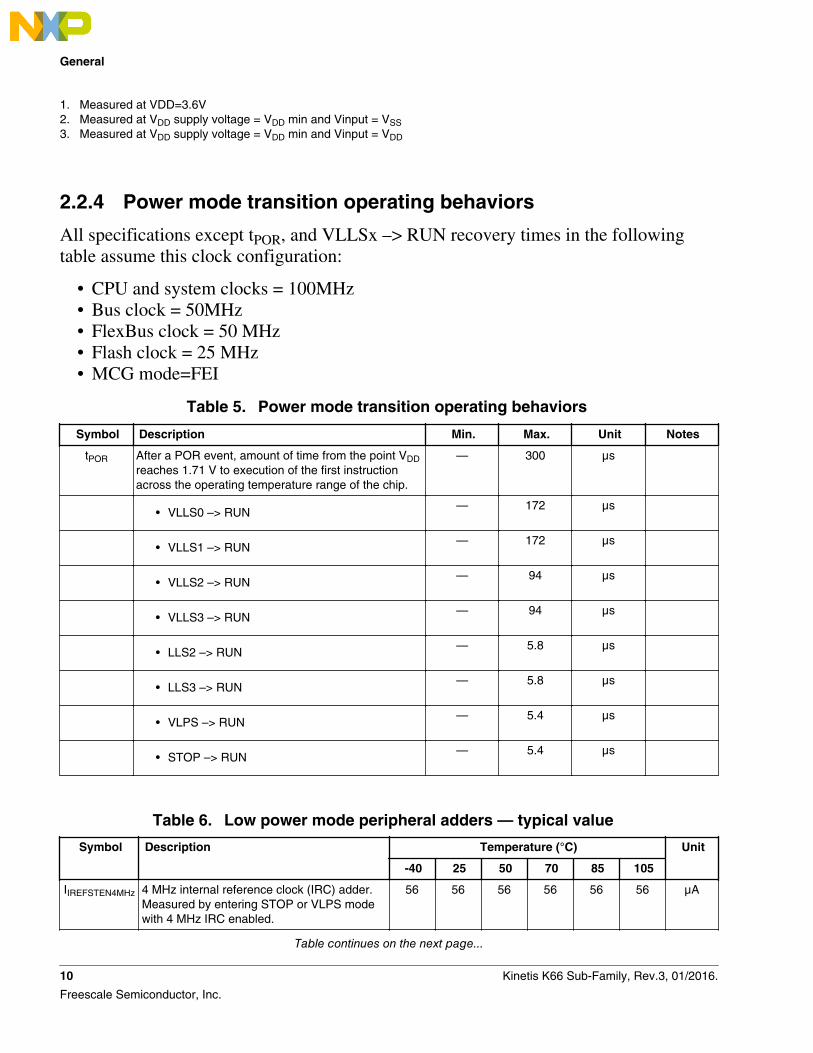
2.2.4 Power mode transition operating behaviors
All specifications except tPOR, and VLLSx –> RUN recovery times in the followingtable assume this clock configuration:
• CPU and system clocks = 100MHz• Bus clock = 50MHz• FlexBus clock = 50 MHz• Flash clock = 25 MHz• MCG mode=FEI
Table 5. Power mode transition operating behaviors
Symbol Description Min. Max. Unit Notes
tPOR After a POR event, amount of time from the point VDDreaches 1.71 V to execution of the first instructionacross the operating temperature range of the chip.
— 300 µs
• VLLS0 –> RUN— 172 µs
• VLLS1 –> RUN— 172 µs
• VLLS2 –> RUN— 94 µs
• VLLS3 –> RUN— 94 µs
• LLS2 –> RUN— 5.8 µs
• LLS3 –> RUN— 5.8 µs
• VLPS –> RUN— 5.4 µs
• STOP –> RUN— 5.4 µs
Table 6. Low power mode peripheral adders — typical value
Symbol Description Temperature (°C) Unit
-40 25 50 70 85 105
IIREFSTEN4MHz 4 MHz internal reference clock (IRC) adder.Measured by entering STOP or VLPS modewith 4 MHz IRC enabled.
56 56 56 56 56 56 µA
Table continues on the next page...
General
10 Kinetis K66 Sub-Family, Rev.3, 01/2016.
Freescale Semiconductor, Inc.
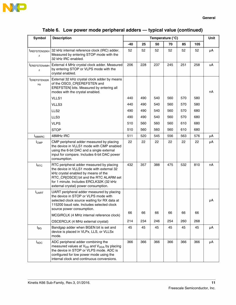
Table 6. Low power mode peripheral adders — typical value (continued)
Symbol Description Temperature (°C) Unit
-40 25 50 70 85 105
IIREFSTEN32KH
z
32 kHz internal reference clock (IRC) adder.Measured by entering STOP mode with the32 kHz IRC enabled.
52 52 52 52 52 52 µA
IEREFSTEN4MH
z
External 4 MHz crystal clock adder. Measuredby entering STOP or VLPS mode with thecrystal enabled.
206 228 237 245 251 258 uA
IEREFSTEN32K
Hz
External 32 kHz crystal clock adder by meansof the OSC0_CR[EREFSTEN andEREFSTEN] bits. Measured by entering allmodes with the crystal enabled.
VLLS1
VLLS3
LLS2
LLS3
VLPS
STOP
440
440
490
490
510
510
490
490
490
490
560
560
540
540
540
540
560
560
560
560
560
560
560
560
570
570
570
570
610
610
580
580
680
680
680
680
nA
I48MIRC 48MHz IRC 511 520 545 556 563 576 µA
ICMP CMP peripheral adder measured by placingthe device in VLLS1 mode with CMP enabledusing the 6-bit DAC and a single externalinput for compare. Includes 6-bit DAC powerconsumption.
22 22 22 22 22 22 µA
IRTC RTC peripheral adder measured by placingthe device in VLLS1 mode with external 32kHz crystal enabled by means of theRTC_CR[OSCE] bit and the RTC ALARM setfor 1 minute. Includes ERCLK32K (32 kHzexternal crystal) power consumption.
432 357 388 475 532 810 nA
IUART UART peripheral adder measured by placingthe device in STOP or VLPS mode withselected clock source waiting for RX data at115200 baud rate. Includes selected clocksource power consumption.
MCGIRCLK (4 MHz internal reference clock)
OSCERCLK (4 MHz external crystal)
66
214
66
234
66
246
66
254
66
260
66
268
µA
IBG Bandgap adder when BGEN bit is set anddevice is placed in VLPx, LLS, or VLLSxmode.
45 45 45 45 45 45 µA
IADC ADC peripheral adder combining themeasured values at VDD and VDDA by placingthe device in STOP or VLPS mode. ADC isconfigured for low power mode using theinternal clock and continuous conversions.
366 366 366 366 366 366 µA
General
Kinetis K66 Sub-Family, Rev.3, 01/2016. 11
Freescale Semiconductor, Inc.
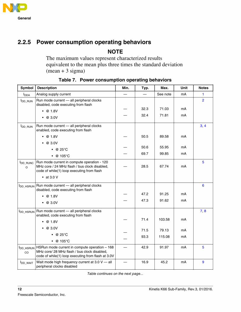
2.2.5 Power consumption operating behaviors
NOTEThe maximum values represent characterized resultsequivalent to the mean plus three times the standard deviation(mean + 3 sigma)
Table 7. Power consumption operating behaviors
Symbol Description Min. Typ. Max. Unit Notes
IDDA Analog supply current — — See note mA 1
IDD_RUN Run mode current — all peripheral clocksdisabled, code executing from flash
• @ 1.8V
• @ 3.0V
—
—
32.3
32.4
71.03
71.81
mA
mA
2
IDD_RUN Run mode current — all peripheral clocksenabled, code executing from flash
• @ 1.8V
• @ 3.0V
• @ 25°C
• @ 105°C
—
—
—
50.5
50.6
69.7
89.58
55.95
99.85
mA
mA
mA
3, 4
IDD_RUNC
O
Run mode current in compute operation - 120MHz core / 24 MHz flash / bus clock disabled,code of while(1) loop executing from flash
• at 3.0 V
— 28.5 67.74 mA5
IDD_HSRUN Run mode current — all peripheral clocksdisabled, code executing from flash
• @ 1.8V
• @ 3.0V
—
—
47.2
47.3
91.25
91.62
mA
mA
6
IDD_HSRUN Run mode current — all peripheral clocksenabled, code executing from flash
• @ 1.8V
• @ 3.0V
• @ 25°C
• @ 105°C
—
—
—
71.4
71.5
93.3
103.58
79.13
115.08
mA
mA
mA
7, 8
IDD_HSRUN
CO
HSRun mode current in compute operation – 168MHz core/ 28 MHz flash / bus clock disabled,code of while(1) loop executing from flash at 3.0V
— 42.9 91.97 mA 5
IDD_WAIT Wait mode high frequency current at 3.0 V — allperipheral clocks disabled
— 16.9 45.2 mA 9
Table continues on the next page...
General
12 Kinetis K66 Sub-Family, Rev.3, 01/2016.
Freescale Semiconductor, Inc.
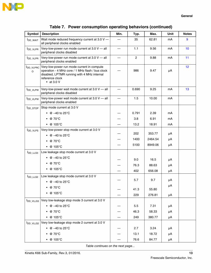
Table 7. Power consumption operating behaviors (continued)
Symbol Description Min. Typ. Max. Unit Notes
IDD_WAIT Wait mode reduced frequency current at 3.0 V —all peripheral clocks enabled
— 35 62.81 mA 9
IDD_VLPR Very-low-power run mode current at 3.0 V — allperipheral clocks disabled
— 1.1 9.56 mA 10
IDD_VLPR Very-low-power run mode current at 3.0 V — allperipheral clocks enabled
— 2 9.88 mA 11
IDD_VLPRC
O
Very-low-power run mode current in computeoperation - 4 MHz core / 1 MHz flash / bus clockdisabled, LPTMR running with 4 MHz internalreference clock
• at 3.0 V
— 986 9.47 μA12
IDD_VLPW Very-low-power wait mode current at 3.0 V — allperipheral clocks disabled
— 0.690 9.25 mA 13
IDD_VLPW Very-low-power wait mode current at 3.0 V — allperipheral clocks enabled
— 1.5 10.00 mA
IDD_STOP Stop mode current at 3.0 V
• @ –40 to 25°C
• @ 70°C
• @ 105°C
—
—
—
0.791
3.8
13.2
2.39
6.91
18.91
mA
mA
mA
IDD_VLPS Very-low-power stop mode current at 3.0 V
• @ –40 to 25°C
• @ 70°C
• @ 105°C
—
—
—
202
1400
5100
353.77
2464.54
8949.06
μA
μA
μA
IDD_LLS3 Low leakage stop mode current at 3.0 V
• @ –40 to 25°C
• @ 70°C
• @ 105°C
—
—
—
9.0
76.3
402
16.5
88.63
656.08
μA
μA
μA
IDD_LLS2 Low leakage stop mode current at 3.0 V
• @ –40 to 25°C
• @ 70°C
• @ 105°C
—
—
—
5.7
41.3
229
9.7
55.80
276.81
μA
μA
μA
IDD_VLLS3 Very low-leakage stop mode 3 current at 3.0 V
• @ –40 to 25°C
• @ 70°C
• @ 105°C
—
—
—
5.5
46.3
249
7.31
58.33
380.77
μA
μA
μA
IDD_VLLS2 Very low-leakage stop mode 2 current at 3.0 V
• @ –40 to 25°C
• @ 70°C
• @ 105°C
—
—
—
2.7
13.1
76.6
3.24
18.72
84.77
μA
μA
μA
Table continues on the next page...
General
Kinetis K66 Sub-Family, Rev.3, 01/2016. 13
Freescale Semiconductor, Inc.
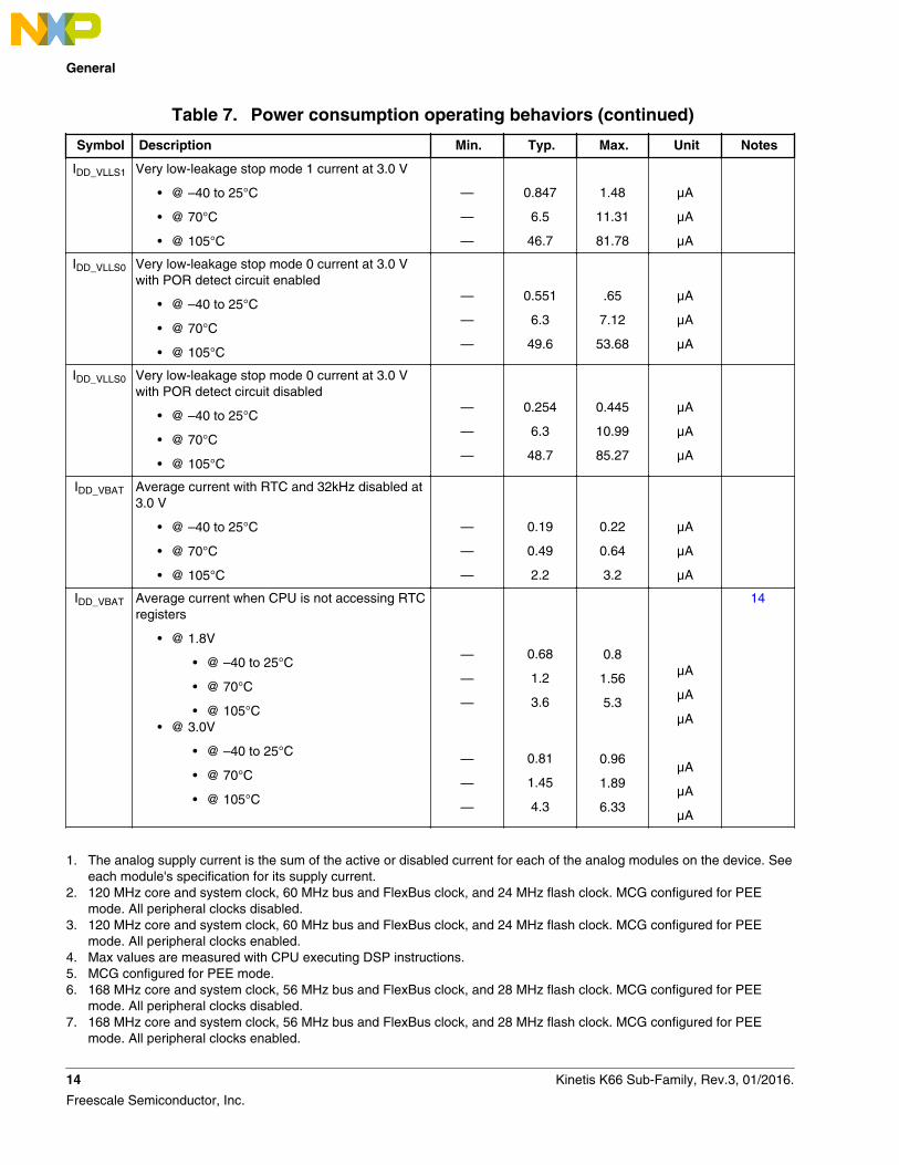
Table 7. Power consumption operating behaviors (continued)
Symbol Description Min. Typ. Max. Unit Notes
IDD_VLLS1 Very low-leakage stop mode 1 current at 3.0 V
• @ –40 to 25°C
• @ 70°C
• @ 105°C
—
—
—
0.847
6.5
46.7
1.48
11.31
81.78
μA
μA
μA
IDD_VLLS0 Very low-leakage stop mode 0 current at 3.0 Vwith POR detect circuit enabled
• @ –40 to 25°C
• @ 70°C
• @ 105°C
—
—
—
0.551
6.3
49.6
.65
7.12
53.68
μA
μA
μA
IDD_VLLS0 Very low-leakage stop mode 0 current at 3.0 Vwith POR detect circuit disabled
• @ –40 to 25°C
• @ 70°C
• @ 105°C
—
—
—
0.254
6.3
48.7
0.445
10.99
85.27
μA
μA
μA
IDD_VBAT Average current with RTC and 32kHz disabled at3.0 V
• @ –40 to 25°C
• @ 70°C
• @ 105°C
—
—
—
0.19
0.49
2.2
0.22
0.64
3.2
μA
μA
μA
IDD_VBAT Average current when CPU is not accessing RTCregisters
• @ 1.8V
• @ –40 to 25°C
• @ 70°C
• @ 105°C• @ 3.0V
• @ –40 to 25°C
• @ 70°C
• @ 105°C
—
—
—
—
—
—
0.68
1.2
3.6
0.81
1.45
4.3
0.8
1.56
5.3
0.96
1.89
6.33
μA
μA
μA
μA
μA
μA
14
1. The analog supply current is the sum of the active or disabled current for each of the analog modules on the device. Seeeach module's specification for its supply current.
2. 120 MHz core and system clock, 60 MHz bus and FlexBus clock, and 24 MHz flash clock. MCG configured for PEEmode. All peripheral clocks disabled.
3. 120 MHz core and system clock, 60 MHz bus and FlexBus clock, and 24 MHz flash clock. MCG configured for PEEmode. All peripheral clocks enabled.
4. Max values are measured with CPU executing DSP instructions.5. MCG configured for PEE mode.6. 168 MHz core and system clock, 56 MHz bus and FlexBus clock, and 28 MHz flash clock. MCG configured for PEE
mode. All peripheral clocks disabled.7. 168 MHz core and system clock, 56 MHz bus and FlexBus clock, and 28 MHz flash clock. MCG configured for PEE
mode. All peripheral clocks enabled.
General
14 Kinetis K66 Sub-Family, Rev.3, 01/2016.
Freescale Semiconductor, Inc.
8. Max values are measured with CPU executing DSP instructions.9. 120 MHz core and system clock, 60MHz bus clock, and FlexBus. MCG configured for PEE mode.10. 4 MHz core, system, FlexBus, and bus clock and 1 MHz flash clock. MCG configured for BLPE mode. All peripheral
clocks disabled. Code executing from flash.11. 4 MHz core, system, FlexBus, and bus clock and 1 MHz flash clock. MCG configured for BLPE mode. All peripheral
clocks enabled but peripherals are not in active operation. Code executing from flash.12. MCG configured for BLPI mode. CoreMark benchmark compiled using IAR 6.40 with optimization level high,
optimized for balanced.13. 4 MHz core, system, FlexBus, and bus clock and 1 MHz flash clock. MCG configured for BLPE mode. All peripheral
clocks disabled.14. Includes 32kHz oscillator current and RTC operation.
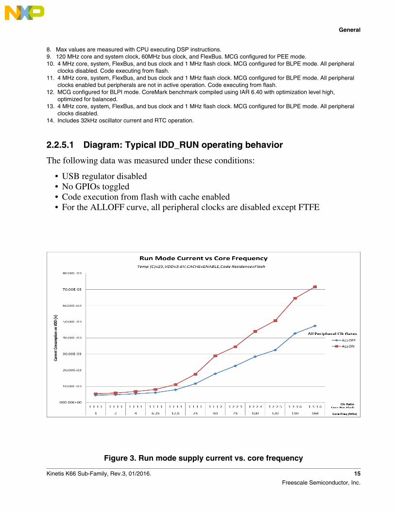
2.2.5.1 Diagram: Typical IDD_RUN operating behavior
The following data was measured under these conditions:
• USB regulator disabled• No GPIOs toggled• Code execution from flash with cache enabled• For the ALLOFF curve, all peripheral clocks are disabled except FTFE
Figure 3. Run mode supply current vs. core frequency
General
Kinetis K66 Sub-Family, Rev.3, 01/2016. 15
Freescale Semiconductor, Inc.
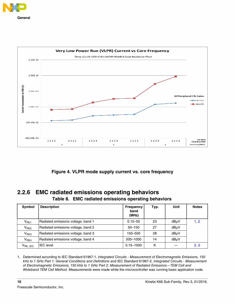
Figure 4. VLPR mode supply current vs. core frequency
2.2.6 EMC radiated emissions operating behaviorsTable 8. EMC radiated emissions operating behaviors
Symbol Description Frequencyband(MHz)
Typ. Unit Notes
VRE1 Radiated emissions voltage, band 1 0.15–50 23 dBμV 1, 2
VRE2 Radiated emissions voltage, band 2 50–150 27 dBμV
VRE3 Radiated emissions voltage, band 3 150–500 28 dBμV
VRE4 Radiated emissions voltage, band 4 500–1000 14 dBμV
VRE_IEC IEC level 0.15–1000 K — 2, 3
1. Determined according to IEC Standard 61967-1, Integrated Circuits - Measurement of Electromagnetic Emissions, 150kHz to 1 GHz Part 1: General Conditions and Definitions and IEC Standard 61967-2, Integrated Circuits - Measurementof Electromagnetic Emissions, 150 kHz to 1 GHz Part 2: Measurement of Radiated Emissions—TEM Cell andWideband TEM Cell Method. Measurements were made while the microcontroller was running basic application code.
General
16 Kinetis K66 Sub-Family, Rev.3, 01/2016.
Freescale Semiconductor, Inc.
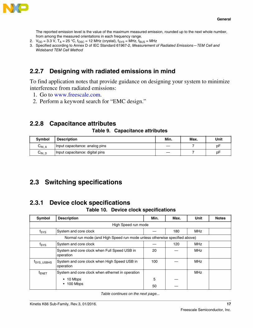
The reported emission level is the value of the maximum measured emission, rounded up to the next whole number,from among the measured orientations in each frequency range.
2. VDD = 3.3 V, TA = 25 °C, fOSC = 12 MHz (crystal), fSYS = MHz, fBUS = MHz3. Specified according to Annex D of IEC Standard 61967-2, Measurement of Radiated Emissions—TEM Cell and
Wideband TEM Cell Method
2.2.7 Designing with radiated emissions in mind
To find application notes that provide guidance on designing your system to minimizeinterference from radiated emissions:
1. Go to www.freescale.com.2. Perform a keyword search for “EMC design.”
2.2.8 Capacitance attributesTable 9. Capacitance attributes
Symbol Description Min. Max. Unit
CIN_A Input capacitance: analog pins — 7 pF
CIN_D Input capacitance: digital pins — 7 pF
2.3 Switching specifications
2.3.1 Device clock specificationsTable 10. Device clock specifications
Symbol Description Min. Max. Unit Notes
High Speed run mode
fSYS System and core clock — 180 MHz
Normal run mode (and High Speed run mode unless otherwise specified above)
fSYS System and core clock — 120 MHz
System and core clock when Full Speed USB inoperation
20 — MHz
fSYS_USBHS System and core clock when High Speed USB inoperation
100 — MHz
fENET System and core clock when ethernet in operation
• 10 Mbps• 100 Mbps
5
50
—
—
MHz
Table continues on the next page...
General
Kinetis K66 Sub-Family, Rev.3, 01/2016. 17
Freescale Semiconductor, Inc.
Table 10. Device clock specifications (continued)
Symbol Description Min. Max. Unit Notes
fBUS Bus clock — 60 MHz
FB_CLK FlexBus clock — 60 MHz
fFLASH Flash clock — 28 MHz
fLPTMR LPTMR clock — 25 MHz
VLPR mode1
fSYS System and core clock — 4 MHz
fBUS Bus clock — 4 MHz
FB_CLK FlexBus clock — 4 MHz
fFLASH Flash clock — 1 MHz
fERCLK External reference clock — 16 MHz
fLPTMR_pin LPTMR clock — 25 MHz
fFlexCAN_ERCLK FlexCAN external reference clock — 8 MHz
fI2S_MCLK I2S master clock — 12.5 MHz
fI2S_BCLK I2S bit clock — 4 MHz
1. The frequency limitations in VLPR mode here override any frequency specification listed in the timing specification forany other module.
2.3.2 General switching specifications
These general purpose specifications apply to all signals configured for GPIO, UART,CAN, CMT, IEEE 1588 timer, timers, and I2C signals.
Table 11. General switching specifications
Symbol Description Min. Max. Unit Notes
GPIO pin interrupt pulse width (digital glitch filterdisabled) — Synchronous path
1.5 — Bus clockcycles
1, 2
GPIO pin interrupt pulse width (digital glitch filterdisabled, analog filter enabled) — Asynchronous path
100 — ns 3
GPIO pin interrupt pulse width (digital glitch filterdisabled, analog filter disabled) — Asynchronous path
50 — ns 3
External reset pulse width (digital glitch filter disabled) 100 — ns 3
Mode select (EZP_CS) hold time after resetdeassertion
2 — Bus clockcycles
Port rise and fall time (high drive strength)
• Slew enabled
—
—
25
15
ns
ns
4
Table continues on the next page...
General
18 Kinetis K66 Sub-Family, Rev.3, 01/2016.
Freescale Semiconductor, Inc.
Table 11. General switching specifications (continued)
Symbol Description Min. Max. Unit Notes
• 1.71 ≤ VDD ≤ 2.7V
• 2.7 ≤ VDD ≤ 3.6V
• Slew disabled
• 1.71 ≤ VDD ≤ 2.7V
• 2.7 ≤ VDD ≤ 3.6V
—
—
7
7
ns
ns
Port rise and fall time (low drive strength)
• Slew enabled
• 1.71 ≤ VDD ≤ 2.7V
• 2.7 ≤ VDD ≤ 3.6V
• Slew disabled
• 1.71 ≤ VDD ≤ 2.7V
• 2.7 ≤ VDD ≤ 3.6V
—
—
—
—
25
15
7
7
ns
ns
ns
ns
5
1. This is the minimum pulse width that is guaranteed to pass through the pin synchronization circuitry. Shorter pulsesmay or may not be recognized. In Stop, VLPS, LLS, and VLLSx modes, the synchronizer is bypassed so shorterpulses can be recognized in that case.
2. The greater synchronous and asynchronous timing must be met.3. This is the minimum pulse width that is guaranteed to be recognized as a pin interrupt request in Stop, VLPS, LLS,
and VLLSx modes.4. 75 pF load5. 15 pF load
2.4 Thermal specifications
2.4.1 Thermal operating requirementsTable 12. Thermal operating requirements
Symbol Description Min. Max. Unit Notes
TJ Die junction temperature –40 125 °C
TA Ambient temperature –40 105 °C 1
1. Maximum TA can be exceeded only if the user ensures that TJ does not exceed maximum TJ. The simplest method todetermine TJ is: TJ = TA + RθJA x chip power dissipation.
General
Kinetis K66 Sub-Family, Rev.3, 01/2016. 19
Freescale Semiconductor, Inc.

2.4.2 Thermal attributes
Board type Symbol Description 144 LQFP 144 MAPBGA Unit Notes
Single-layer(1s)
RθJA Thermalresistance,junction toambient(naturalconvection)
45 48 °C/W 1
Four-layer(2s2p)
RθJA Thermalresistance,junction toambient(naturalconvection)
36 29 °C/W 1
Single-layer(1s)
RθJMA Thermalresistance,junction toambient (200ft./min. airspeed)
36 38 °C/W 1
Four-layer(2s2p)
RθJMA Thermalresistance,junction toambient (200ft./min. airspeed)
30 25 °C/W 1
— RθJB Thermalresistance,junction toboard
24 16 °C/W 2
— RθJC Thermalresistance,junction to case
9 9 °C/W 3
— ΨJT Thermalcharacterizationparameter,junction topackage topoutside center(naturalconvection)
2 2 °C/W 4
NOTES:1. Determined according to JEDEC Standard JESD51-2, Integrated Circuits Thermal
Test Method Environmental Conditions—Natural Convection (Still Air) with thesingle layer board horizontal. Board meets JESD51-9 specification.
2. Determined according to JEDEC Standard JESD51-8, Integrated Circuit ThermalTest Method Environmental Conditions—Junction-to-Board.
General
20 Kinetis K66 Sub-Family, Rev.3, 01/2016.
Freescale Semiconductor, Inc.
3. Determined according to Method 1012.1 of MIL-STD 883, Test MethodStandard, Microcircuits, with the cold plate temperature used for the casetemperature. The value includes the thermal resistance of the interface materialbetween the top of the package and the cold plate.
4. Determined according to JEDEC Standard JESD51-2, Integrated CircuitsThermal Test Method Environmental Conditions—Natural Convection (Still Air).
3 Peripheral operating requirements and behaviors
3.1 Core modules
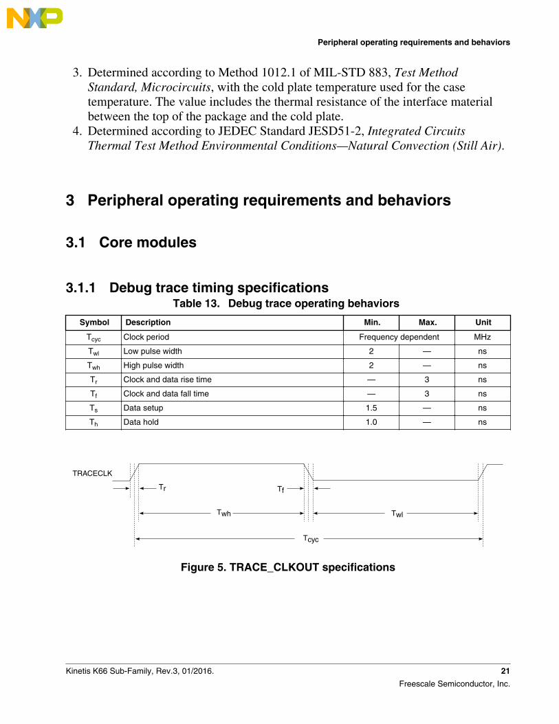
3.1.1 Debug trace timing specificationsTable 13. Debug trace operating behaviors
Symbol Description Min. Max. Unit
Tcyc Clock period Frequency dependent MHz
Twl Low pulse width 2 — ns
Twh High pulse width 2 — ns
Tr Clock and data rise time — 3 ns
Tf Clock and data fall time — 3 ns
Ts Data setup 1.5 — ns
Th Data hold 1.0 — ns
TRACECLK
Tr
Twh
Tf
Tcyc
Twl
Figure 5. TRACE_CLKOUT specifications
Peripheral operating requirements and behaviors
Kinetis K66 Sub-Family, Rev.3, 01/2016. 21
Freescale Semiconductor, Inc.
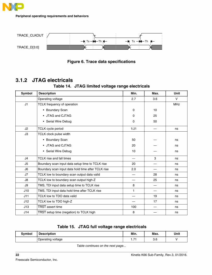
ThTs Ts Th
TRACE_CLKOUT
TRACE_D[3:0]
Figure 6. Trace data specifications
3.1.2 JTAG electricalsTable 14. JTAG limited voltage range electricals
Symbol Description Min. Max. Unit
Operating voltage 2.7 3.6 V
J1 TCLK frequency of operation
• Boundary Scan
• JTAG and CJTAG
• Serial Wire Debug
0
0
0
10
25
50
MHz
J2 TCLK cycle period 1/J1 — ns
J3 TCLK clock pulse width
• Boundary Scan
• JTAG and CJTAG
• Serial Wire Debug
50
20
10
—
—
—
ns
ns
ns
J4 TCLK rise and fall times — 3 ns
J5 Boundary scan input data setup time to TCLK rise 20 — ns
J6 Boundary scan input data hold time after TCLK rise 2.0 — ns
J7 TCLK low to boundary scan output data valid — 28 ns
J8 TCLK low to boundary scan output high-Z — 25 ns
J9 TMS, TDI input data setup time to TCLK rise 8 — ns
J10 TMS, TDI input data hold time after TCLK rise 1 — ns
J11 TCLK low to TDO data valid — 19 ns
J12 TCLK low to TDO high-Z — 17 ns
J13 TRST assert time 100 — ns
J14 TRST setup time (negation) to TCLK high 8 — ns
Table 15. JTAG full voltage range electricals
Symbol Description Min. Max. Unit
Operating voltage 1.71 3.6 V
Table continues on the next page...
Peripheral operating requirements and behaviors
22 Kinetis K66 Sub-Family, Rev.3, 01/2016.
Freescale Semiconductor, Inc.
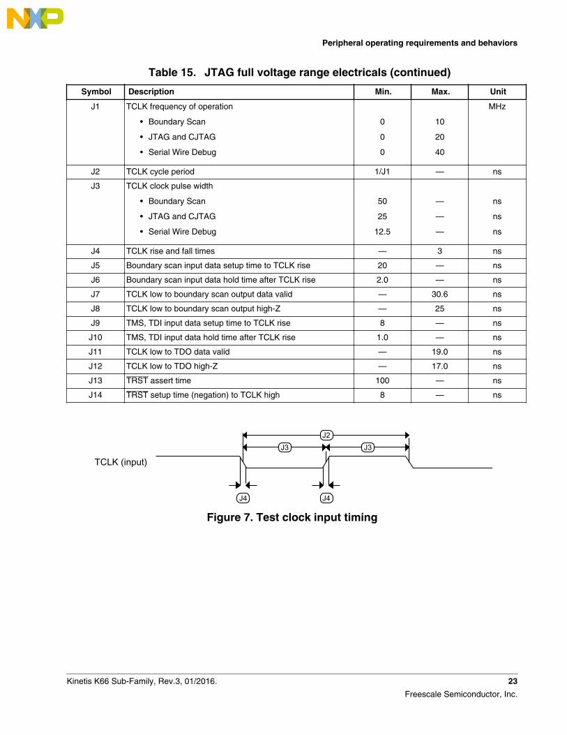
Table 15. JTAG full voltage range electricals (continued)
Symbol Description Min. Max. Unit
J1 TCLK frequency of operation
• Boundary Scan
• JTAG and CJTAG
• Serial Wire Debug
0
0
0
10
20
40
MHz
J2 TCLK cycle period 1/J1 — ns
J3 TCLK clock pulse width
• Boundary Scan
• JTAG and CJTAG
• Serial Wire Debug
50
25
12.5
—
—
—
ns
ns
ns
J4 TCLK rise and fall times — 3 ns
J5 Boundary scan input data setup time to TCLK rise 20 — ns
J6 Boundary scan input data hold time after TCLK rise 2.0 — ns
J7 TCLK low to boundary scan output data valid — 30.6 ns
J8 TCLK low to boundary scan output high-Z — 25 ns
J9 TMS, TDI input data setup time to TCLK rise 8 — ns
J10 TMS, TDI input data hold time after TCLK rise 1.0 — ns
J11 TCLK low to TDO data valid — 19.0 ns
J12 TCLK low to TDO high-Z — 17.0 ns
J13 TRST assert time 100 — ns
J14 TRST setup time (negation) to TCLK high 8 — ns
J2J3 J3
J4 J4
TCLK (input)
Figure 7. Test clock input timing
Peripheral operating requirements and behaviors
Kinetis K66 Sub-Family, Rev.3, 01/2016. 23
Freescale Semiconductor, Inc.
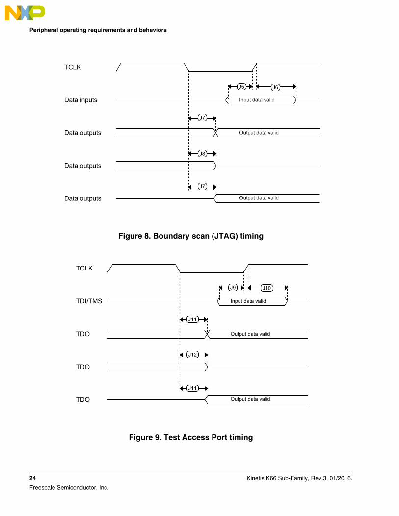
J7
J8
J7
J5 J6
Input data valid
Output data valid
Output data valid
TCLK
Data inputs
Data outputs
Data outputs
Data outputs
Figure 8. Boundary scan (JTAG) timing
J11
J12
J11
J9 J10
Input data valid
Output data valid
Output data valid
TCLK
TDI/TMS
TDO
TDO
TDO
Figure 9. Test Access Port timing
Peripheral operating requirements and behaviors
24 Kinetis K66 Sub-Family, Rev.3, 01/2016.
Freescale Semiconductor, Inc.
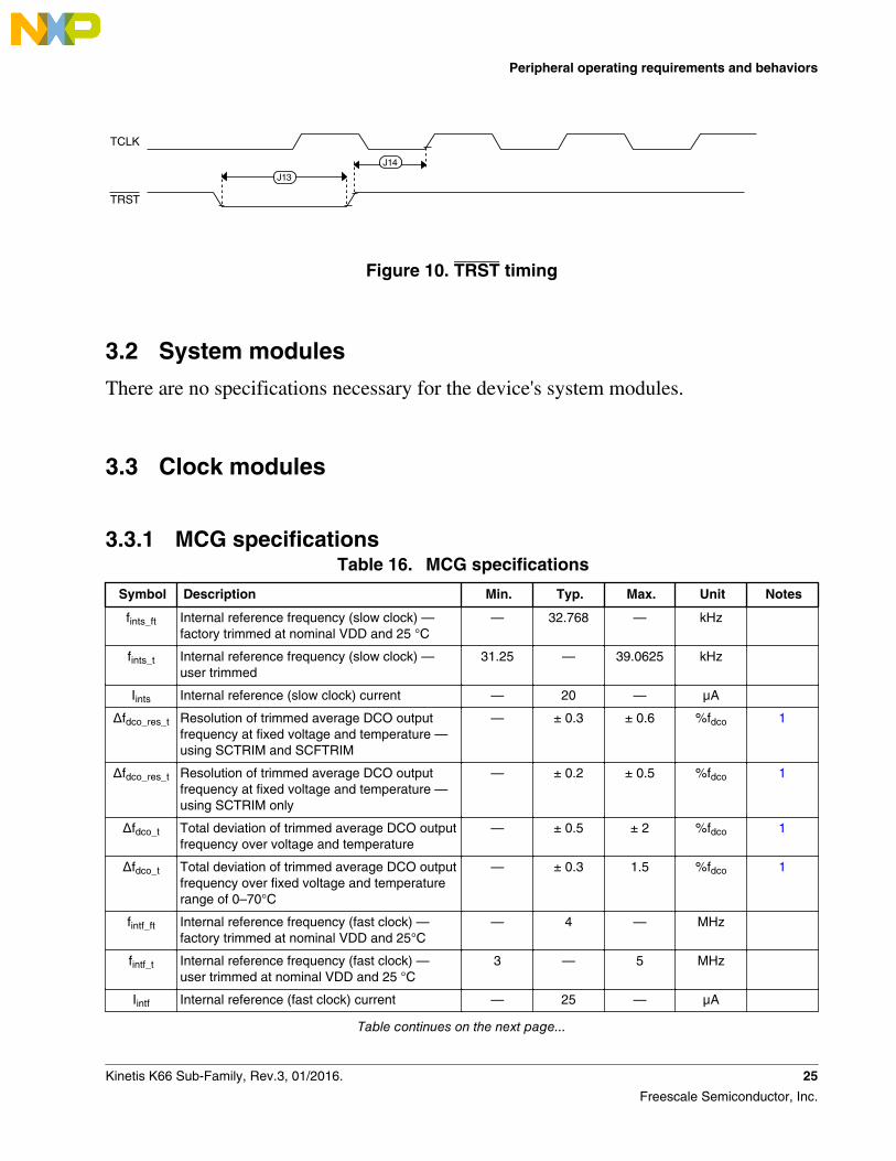
J14
J13
TCLK
TRST
Figure 10. TRST timing
3.2 System modules
There are no specifications necessary for the device's system modules.
3.3 Clock modules
3.3.1 MCG specificationsTable 16. MCG specifications
Symbol Description Min. Typ. Max. Unit Notes
fints_ft Internal reference frequency (slow clock) —factory trimmed at nominal VDD and 25 °C
— 32.768 — kHz
fints_t Internal reference frequency (slow clock) —user trimmed
31.25 — 39.0625 kHz
Iints Internal reference (slow clock) current — 20 — µA
Δfdco_res_t Resolution of trimmed average DCO outputfrequency at fixed voltage and temperature —using SCTRIM and SCFTRIM
— ± 0.3 ± 0.6 %fdco 1
Δfdco_res_t Resolution of trimmed average DCO outputfrequency at fixed voltage and temperature —using SCTRIM only
— ± 0.2 ± 0.5 %fdco 1
Δfdco_t Total deviation of trimmed average DCO outputfrequency over voltage and temperature
— ± 0.5 ± 2 %fdco 1
Δfdco_t Total deviation of trimmed average DCO outputfrequency over fixed voltage and temperaturerange of 0–70°C
— ± 0.3 1.5 %fdco 1
fintf_ft Internal reference frequency (fast clock) —factory trimmed at nominal VDD and 25°C
— 4 — MHz
fintf_t Internal reference frequency (fast clock) —user trimmed at nominal VDD and 25 °C
3 — 5 MHz
Iintf Internal reference (fast clock) current — 25 — µA
Table continues on the next page...
Peripheral operating requirements and behaviors
Kinetis K66 Sub-Family, Rev.3, 01/2016. 25
Freescale Semiconductor, Inc.
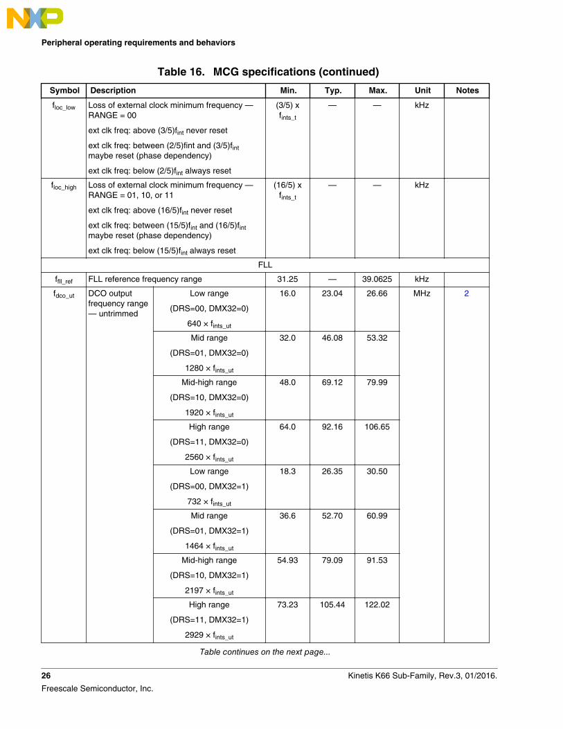
Table 16. MCG specifications (continued)
Symbol Description Min. Typ. Max. Unit Notes
floc_low Loss of external clock minimum frequency —RANGE = 00
ext clk freq: above (3/5)fint never reset
ext clk freq: between (2/5)fint and (3/5)fintmaybe reset (phase dependency)
ext clk freq: below (2/5)fint always reset
(3/5) xfints_t
— — kHz
floc_high Loss of external clock minimum frequency —RANGE = 01, 10, or 11
ext clk freq: above (16/5)fint never reset
ext clk freq: between (15/5)fint and (16/5)fintmaybe reset (phase dependency)
ext clk freq: below (15/5)fint always reset
(16/5) xfints_t
— — kHz
FLL
ffll_ref FLL reference frequency range 31.25 — 39.0625 kHz
fdco_ut DCO outputfrequency range— untrimmed
Low range
(DRS=00, DMX32=0)
640 × fints_ut
16.0 23.04 26.66 MHz 2
Mid range
(DRS=01, DMX32=0)
1280 × fints_ut
32.0 46.08 53.32
Mid-high range
(DRS=10, DMX32=0)
1920 × fints_ut
48.0 69.12 79.99
High range
(DRS=11, DMX32=0)
2560 × fints_ut
64.0 92.16 106.65
Low range
(DRS=00, DMX32=1)
732 × fints_ut
18.3 26.35 30.50
Mid range
(DRS=01, DMX32=1)
1464 × fints_ut
36.6 52.70 60.99
Mid-high range
(DRS=10, DMX32=1)
2197 × fints_ut
54.93 79.09 91.53
High range
(DRS=11, DMX32=1)
2929 × fints_ut
73.23 105.44 122.02
Table continues on the next page...
Peripheral operating requirements and behaviors
26 Kinetis K66 Sub-Family, Rev.3, 01/2016.
Freescale Semiconductor, Inc.
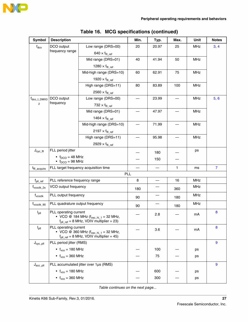
Table 16. MCG specifications (continued)
Symbol Description Min. Typ. Max. Unit Notes
fdco DCO outputfrequency range
Low range (DRS=00)
640 × ffll_ref
20 20.97 25 MHz 3, 4
Mid range (DRS=01)
1280 × ffll_ref
40 41.94 50 MHz
Mid-high range (DRS=10)
1920 × ffll_ref
60 62.91 75 MHz
High range (DRS=11)
2560 × ffll_ref
80 83.89 100 MHz
fdco_t_DMX3
2
DCO outputfrequency
Low range (DRS=00)
732 × ffll_ref
— 23.99 — MHz 5, 6
Mid range (DRS=01)
1464 × ffll_ref
— 47.97 — MHz
Mid-high range (DRS=10)
2197 × ffll_ref
— 71.99 — MHz
High range (DRS=11)
2929 × ffll_ref
— 95.98 — MHz
Jcyc_fll FLL period jitter
• fDCO = 48 MHz• fDCO = 98 MHz
—
—
180
150
—
—
ps
tfll_acquire FLL target frequency acquisition time — — 1 ms 7
PLL
fpll_ref PLL reference frequency range 8 — 16 MHz
fvcoclk_2x VCO output frequency180
—360
MHz
fvcoclk PLL output frequency90
—180
MHz
fvcoclk_90 PLL quadrature output frequency90
—180
MHz
Ipll PLL operating current• VCO @ 184 MHz (fosc_hi_1 = 32 MHz,
fpll_ref = 8 MHz, VDIV multiplier = 23)
— 2.8 — mA8
Ipll PLL operating current• VCO @ 360 MHz (fosc_hi_1 = 32 MHz,
fpll_ref = 8 MHz, VDIV multiplier = 45)
— 3.6 — mA8
Jcyc_pll PLL period jitter (RMS)
• fvco = 180 MHz
• fvco = 360 MHz
—
—
100
75
—
—
ps
ps
9
Jacc_pll PLL accumulated jitter over 1µs (RMS)
• fvco = 180 MHz
• fvco = 360 MHz
—
—
600
300
—
—
ps
ps
9
Table continues on the next page...
Peripheral operating requirements and behaviors
Kinetis K66 Sub-Family, Rev.3, 01/2016. 27
Freescale Semiconductor, Inc.
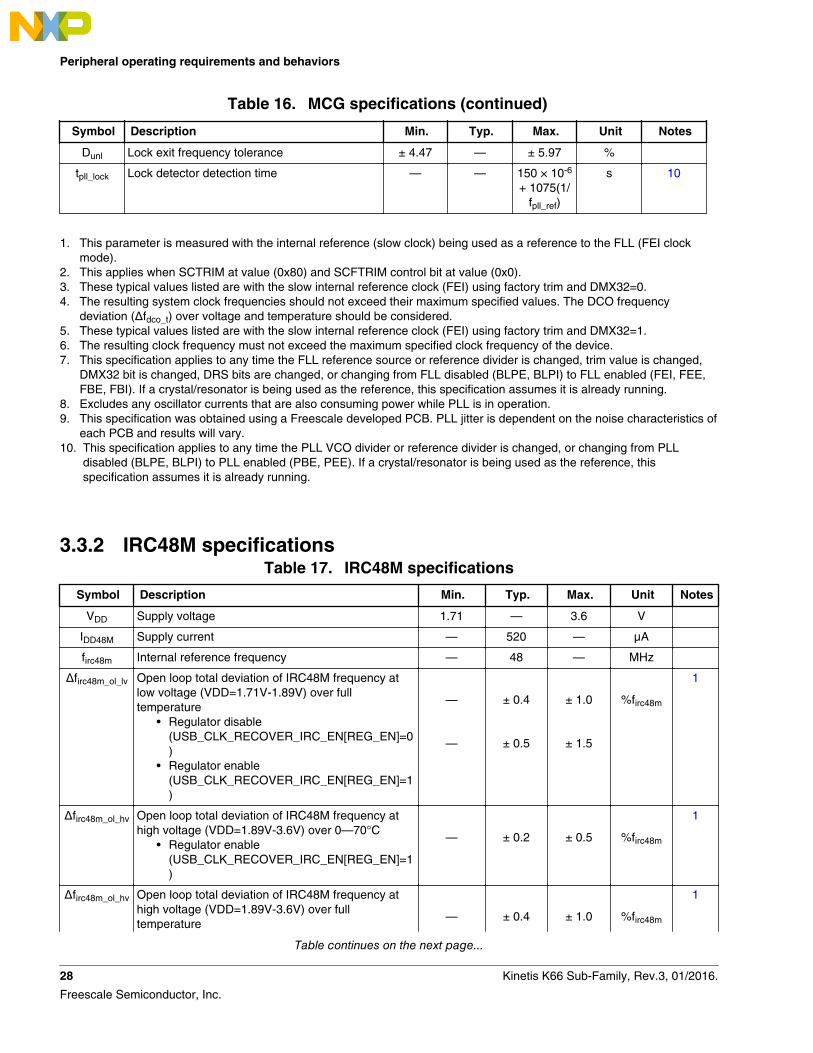
Table 16. MCG specifications (continued)
Symbol Description Min. Typ. Max. Unit Notes
Dunl Lock exit frequency tolerance ± 4.47 — ± 5.97 %
tpll_lock Lock detector detection time — — 150 × 10-6
+ 1075(1/fpll_ref)
s 10
1. This parameter is measured with the internal reference (slow clock) being used as a reference to the FLL (FEI clockmode).
2. This applies when SCTRIM at value (0x80) and SCFTRIM control bit at value (0x0).3. These typical values listed are with the slow internal reference clock (FEI) using factory trim and DMX32=0.4. The resulting system clock frequencies should not exceed their maximum specified values. The DCO frequency
deviation (Δfdco_t) over voltage and temperature should be considered.5. These typical values listed are with the slow internal reference clock (FEI) using factory trim and DMX32=1.6. The resulting clock frequency must not exceed the maximum specified clock frequency of the device.7. This specification applies to any time the FLL reference source or reference divider is changed, trim value is changed,
DMX32 bit is changed, DRS bits are changed, or changing from FLL disabled (BLPE, BLPI) to FLL enabled (FEI, FEE,FBE, FBI). If a crystal/resonator is being used as the reference, this specification assumes it is already running.
8. Excludes any oscillator currents that are also consuming power while PLL is in operation.9. This specification was obtained using a Freescale developed PCB. PLL jitter is dependent on the noise characteristics of
each PCB and results will vary.10. This specification applies to any time the PLL VCO divider or reference divider is changed, or changing from PLL
disabled (BLPE, BLPI) to PLL enabled (PBE, PEE). If a crystal/resonator is being used as the reference, thisspecification assumes it is already running.
3.3.2 IRC48M specificationsTable 17. IRC48M specifications
Symbol Description Min. Typ. Max. Unit Notes
VDD Supply voltage 1.71 — 3.6 V
IDD48M Supply current — 520 — μA
firc48m Internal reference frequency — 48 — MHz
Δfirc48m_ol_lv Open loop total deviation of IRC48M frequency atlow voltage (VDD=1.71V-1.89V) over fulltemperature
• Regulator disable(USB_CLK_RECOVER_IRC_EN[REG_EN]=0)
• Regulator enable(USB_CLK_RECOVER_IRC_EN[REG_EN]=1)
—
—
± 0.4
± 0.5
± 1.0
± 1.5
%firc48m
1
Δfirc48m_ol_hv Open loop total deviation of IRC48M frequency athigh voltage (VDD=1.89V-3.6V) over 0—70°C
• Regulator enable(USB_CLK_RECOVER_IRC_EN[REG_EN]=1)
—
± 0.2
± 0.5
%firc48m
1
Δfirc48m_ol_hv Open loop total deviation of IRC48M frequency athigh voltage (VDD=1.89V-3.6V) over fulltemperature
—
± 0.4
± 1.0
%firc48m
1
Table continues on the next page...
Peripheral operating requirements and behaviors
28 Kinetis K66 Sub-Family, Rev.3, 01/2016.
Freescale Semiconductor, Inc.
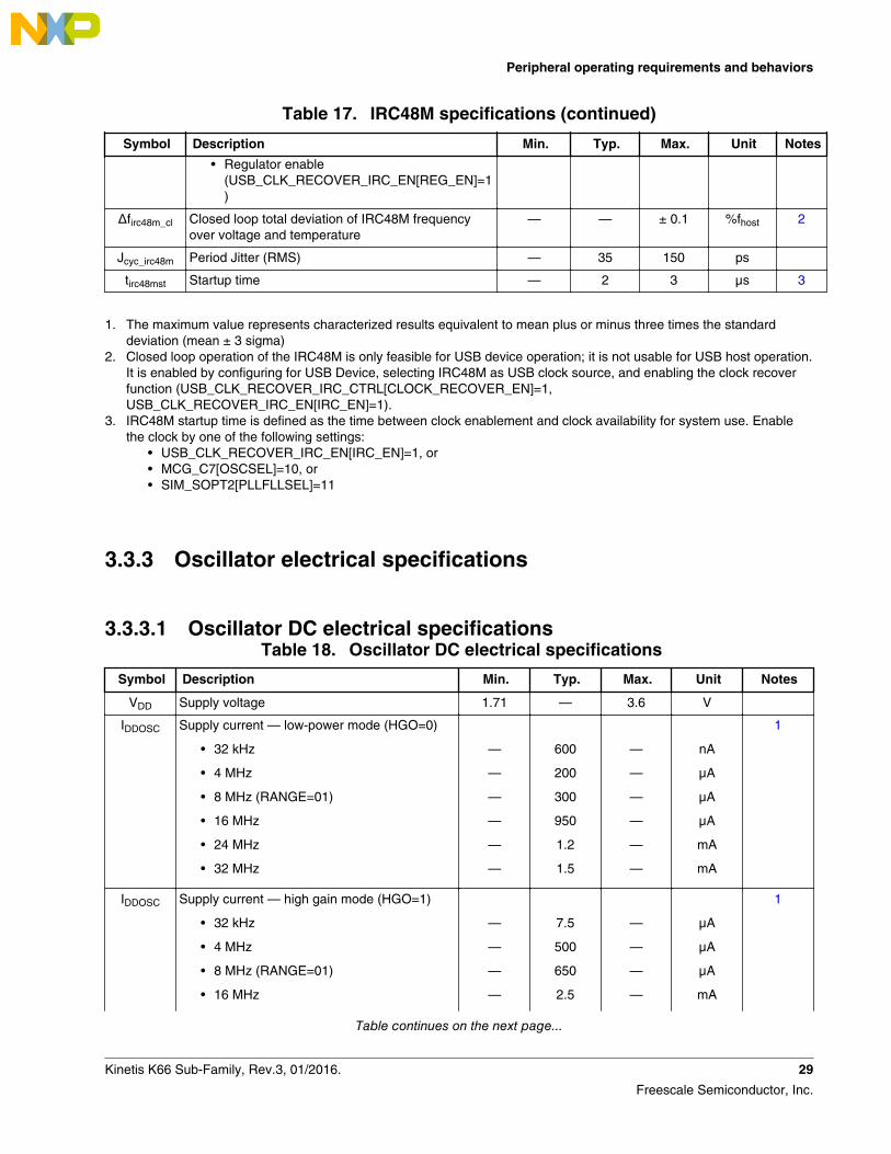
Table 17. IRC48M specifications (continued)
Symbol Description Min. Typ. Max. Unit Notes
• Regulator enable(USB_CLK_RECOVER_IRC_EN[REG_EN]=1)
Δfirc48m_cl Closed loop total deviation of IRC48M frequencyover voltage and temperature
— — ± 0.1 %fhost 2
Jcyc_irc48m Period Jitter (RMS) — 35 150 ps
tirc48mst Startup time — 2 3 μs 3
1. The maximum value represents characterized results equivalent to mean plus or minus three times the standarddeviation (mean ± 3 sigma)
2. Closed loop operation of the IRC48M is only feasible for USB device operation; it is not usable for USB host operation.It is enabled by configuring for USB Device, selecting IRC48M as USB clock source, and enabling the clock recoverfunction (USB_CLK_RECOVER_IRC_CTRL[CLOCK_RECOVER_EN]=1,USB_CLK_RECOVER_IRC_EN[IRC_EN]=1).
3. IRC48M startup time is defined as the time between clock enablement and clock availability for system use. Enablethe clock by one of the following settings:
• USB_CLK_RECOVER_IRC_EN[IRC_EN]=1, or• MCG_C7[OSCSEL]=10, or• SIM_SOPT2[PLLFLLSEL]=11
3.3.3 Oscillator electrical specifications
3.3.3.1 Oscillator DC electrical specificationsTable 18. Oscillator DC electrical specifications
Symbol Description Min. Typ. Max. Unit Notes
VDD Supply voltage 1.71 — 3.6 V
IDDOSC Supply current — low-power mode (HGO=0)
• 32 kHz
• 4 MHz
• 8 MHz (RANGE=01)
• 16 MHz
• 24 MHz
• 32 MHz
—
—
—
—
—
—
600
200
300
950
1.2
1.5
—
—
—
—
—
—
nA
μA
μA
μA
mA
mA
1
IDDOSC Supply current — high gain mode (HGO=1)
• 32 kHz
• 4 MHz
• 8 MHz (RANGE=01)
• 16 MHz
—
—
—
—
7.5
500
650
2.5
—
—
—
—
μA
μA
μA
mA
1
Table continues on the next page...
Peripheral operating requirements and behaviors
Kinetis K66 Sub-Family, Rev.3, 01/2016. 29
Freescale Semiconductor, Inc.
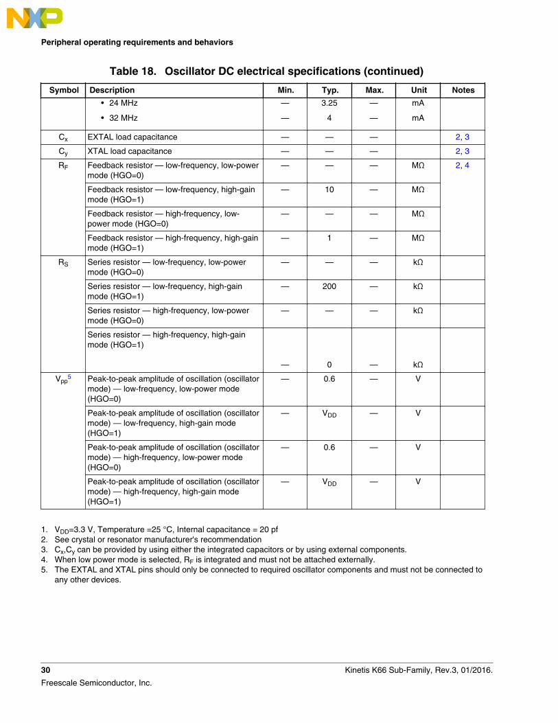
Table 18. Oscillator DC electrical specifications (continued)
Symbol Description Min. Typ. Max. Unit Notes
• 24 MHz
• 32 MHz
—
—
3.25
4
—
—
mA
mA
Cx EXTAL load capacitance — — — 2, 3
Cy XTAL load capacitance — — — 2, 3
RF Feedback resistor — low-frequency, low-powermode (HGO=0)
— — — MΩ 2, 4
Feedback resistor — low-frequency, high-gainmode (HGO=1)
— 10 — MΩ
Feedback resistor — high-frequency, low-power mode (HGO=0)
— — — MΩ
Feedback resistor — high-frequency, high-gainmode (HGO=1)
— 1 — MΩ
RS Series resistor — low-frequency, low-powermode (HGO=0)
— — — kΩ
Series resistor — low-frequency, high-gainmode (HGO=1)
— 200 — kΩ
Series resistor — high-frequency, low-powermode (HGO=0)
— — — kΩ
Series resistor — high-frequency, high-gainmode (HGO=1)
—
0
—
kΩ
Vpp5 Peak-to-peak amplitude of oscillation (oscillator
mode) — low-frequency, low-power mode(HGO=0)
— 0.6 — V
Peak-to-peak amplitude of oscillation (oscillatormode) — low-frequency, high-gain mode(HGO=1)
— VDD — V
Peak-to-peak amplitude of oscillation (oscillatormode) — high-frequency, low-power mode(HGO=0)
— 0.6 — V
Peak-to-peak amplitude of oscillation (oscillatormode) — high-frequency, high-gain mode(HGO=1)
— VDD — V
1. VDD=3.3 V, Temperature =25 °C, Internal capacitance = 20 pf2. See crystal or resonator manufacturer's recommendation3. Cx,Cy can be provided by using either the integrated capacitors or by using external components.4. When low power mode is selected, RF is integrated and must not be attached externally.5. The EXTAL and XTAL pins should only be connected to required oscillator components and must not be connected to
any other devices.
Peripheral operating requirements and behaviors
30 Kinetis K66 Sub-Family, Rev.3, 01/2016.
Freescale Semiconductor, Inc.
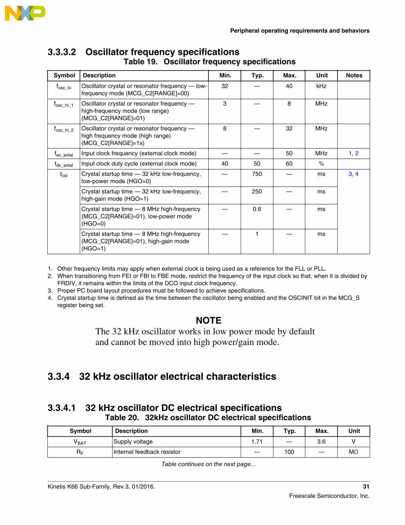
3.3.3.2 Oscillator frequency specificationsTable 19. Oscillator frequency specifications
Symbol Description Min. Typ. Max. Unit Notes
fosc_lo Oscillator crystal or resonator frequency — low-frequency mode (MCG_C2[RANGE]=00)
32 — 40 kHz
fosc_hi_1 Oscillator crystal or resonator frequency —high-frequency mode (low range)(MCG_C2[RANGE]=01)
3 — 8 MHz
fosc_hi_2 Oscillator crystal or resonator frequency —high frequency mode (high range)(MCG_C2[RANGE]=1x)
8 — 32 MHz
fec_extal Input clock frequency (external clock mode) — — 50 MHz 1, 2
tdc_extal Input clock duty cycle (external clock mode) 40 50 60 %
tcst Crystal startup time — 32 kHz low-frequency,low-power mode (HGO=0)
— 750 — ms 3, 4
Crystal startup time — 32 kHz low-frequency,high-gain mode (HGO=1)
— 250 — ms
Crystal startup time — 8 MHz high-frequency(MCG_C2[RANGE]=01), low-power mode(HGO=0)
— 0.6 — ms
Crystal startup time — 8 MHz high-frequency(MCG_C2[RANGE]=01), high-gain mode(HGO=1)
— 1 — ms
1. Other frequency limits may apply when external clock is being used as a reference for the FLL or PLL.2. When transitioning from FEI or FBI to FBE mode, restrict the frequency of the input clock so that, when it is divided by
FRDIV, it remains within the limits of the DCO input clock frequency.3. Proper PC board layout procedures must be followed to achieve specifications.4. Crystal startup time is defined as the time between the oscillator being enabled and the OSCINIT bit in the MCG_S
register being set.
NOTEThe 32 kHz oscillator works in low power mode by defaultand cannot be moved into high power/gain mode.
3.3.4 32 kHz oscillator electrical characteristics
3.3.4.1 32 kHz oscillator DC electrical specificationsTable 20. 32kHz oscillator DC electrical specifications
Symbol Description Min. Typ. Max. Unit
VBAT Supply voltage 1.71 — 3.6 V
RF Internal feedback resistor — 100 — MΩ
Table continues on the next page...
Peripheral operating requirements and behaviors
Kinetis K66 Sub-Family, Rev.3, 01/2016. 31
Freescale Semiconductor, Inc.
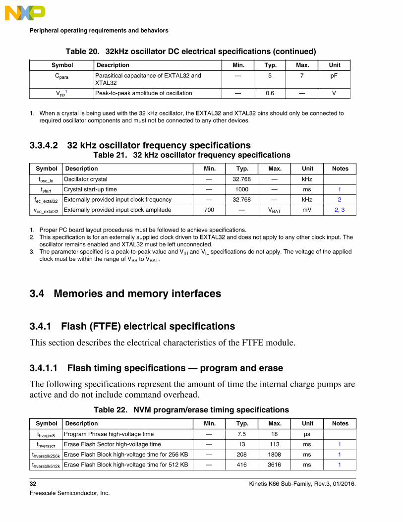
Table 20. 32kHz oscillator DC electrical specifications (continued)
Symbol Description Min. Typ. Max. Unit
Cpara Parasitical capacitance of EXTAL32 andXTAL32
— 5 7 pF
Vpp1 Peak-to-peak amplitude of oscillation — 0.6 — V
1. When a crystal is being used with the 32 kHz oscillator, the EXTAL32 and XTAL32 pins should only be connected torequired oscillator components and must not be connected to any other devices.
3.3.4.2 32 kHz oscillator frequency specificationsTable 21. 32 kHz oscillator frequency specifications
Symbol Description Min. Typ. Max. Unit Notes
fosc_lo Oscillator crystal — 32.768 — kHz
tstart Crystal start-up time — 1000 — ms 1
fec_extal32 Externally provided input clock frequency — 32.768 — kHz 2
vec_extal32 Externally provided input clock amplitude 700 — VBAT mV 2, 3
1. Proper PC board layout procedures must be followed to achieve specifications.2. This specification is for an externally supplied clock driven to EXTAL32 and does not apply to any other clock input. The
oscillator remains enabled and XTAL32 must be left unconnected.3. The parameter specified is a peak-to-peak value and VIH and VIL specifications do not apply. The voltage of the applied
clock must be within the range of VSS to VBAT.
3.4 Memories and memory interfaces
3.4.1 Flash (FTFE) electrical specifications
This section describes the electrical characteristics of the FTFE module.
3.4.1.1 Flash timing specifications — program and erase
The following specifications represent the amount of time the internal charge pumps areactive and do not include command overhead.
Table 22. NVM program/erase timing specifications
Symbol Description Min. Typ. Max. Unit Notes
thvpgm8 Program Phrase high-voltage time — 7.5 18 μs
thversscr Erase Flash Sector high-voltage time — 13 113 ms 1
thversblk256k Erase Flash Block high-voltage time for 256 KB — 208 1808 ms 1
thversblk512k Erase Flash Block high-voltage time for 512 KB — 416 3616 ms 1
Peripheral operating requirements and behaviors
32 Kinetis K66 Sub-Family, Rev.3, 01/2016.
Freescale Semiconductor, Inc.
1. Maximum time based on expectations at cycling end-of-life.
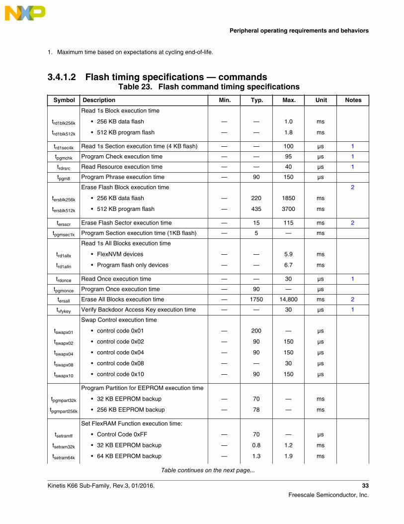
3.4.1.2 Flash timing specifications — commandsTable 23. Flash command timing specifications
Symbol Description Min. Typ. Max. Unit Notes
trd1blk256k
trd1blk512k
Read 1s Block execution time
• 256 KB data flash
• 512 KB program flash
—
—
—
—
1.0
1.8
ms
ms
trd1sec4k Read 1s Section execution time (4 KB flash) — — 100 μs 1
tpgmchk Program Check execution time — — 95 μs 1
trdrsrc Read Resource execution time — — 40 μs 1
tpgm8 Program Phrase execution time — 90 150 μs
tersblk256k
tersblk512k
Erase Flash Block execution time
• 256 KB data flash
• 512 KB program flash
—
—
220
435
1850
3700
ms
ms
2
tersscr Erase Flash Sector execution time — 15 115 ms 2
tpgmsec1k Program Section execution time (1KB flash) — 5 — ms
trd1allx
trd1alln
Read 1s All Blocks execution time
• FlexNVM devices
• Program flash only devices
—
—
—
—
5.9
6.7
ms
ms
trdonce Read Once execution time — — 30 μs 1
tpgmonce Program Once execution time — 90 — μs
tersall Erase All Blocks execution time — 1750 14,800 ms 2
tvfykey Verify Backdoor Access Key execution time — — 30 μs 1
tswapx01
tswapx02
tswapx04
tswapx08
tswapx10
Swap Control execution time
• control code 0x01
• control code 0x02
• control code 0x04
• control code 0x08
• control code 0x10
—
—
—
—
—
200
90
90
—
90
—
150
150
30
150
μs
μs
μs
μs
μs
tpgmpart32k
tpgmpart256k
Program Partition for EEPROM execution time
• 32 KB EEPROM backup
• 256 KB EEPROM backup
—
—
70
78
—
—
ms
ms
tsetramff
tsetram32k
tsetram64k
Set FlexRAM Function execution time:
• Control Code 0xFF
• 32 KB EEPROM backup
• 64 KB EEPROM backup
—
—
—
70
0.8
1.3
—
1.2
1.9
μs
ms
ms
Table continues on the next page...
Peripheral operating requirements and behaviors
Kinetis K66 Sub-Family, Rev.3, 01/2016. 33
Freescale Semiconductor, Inc.
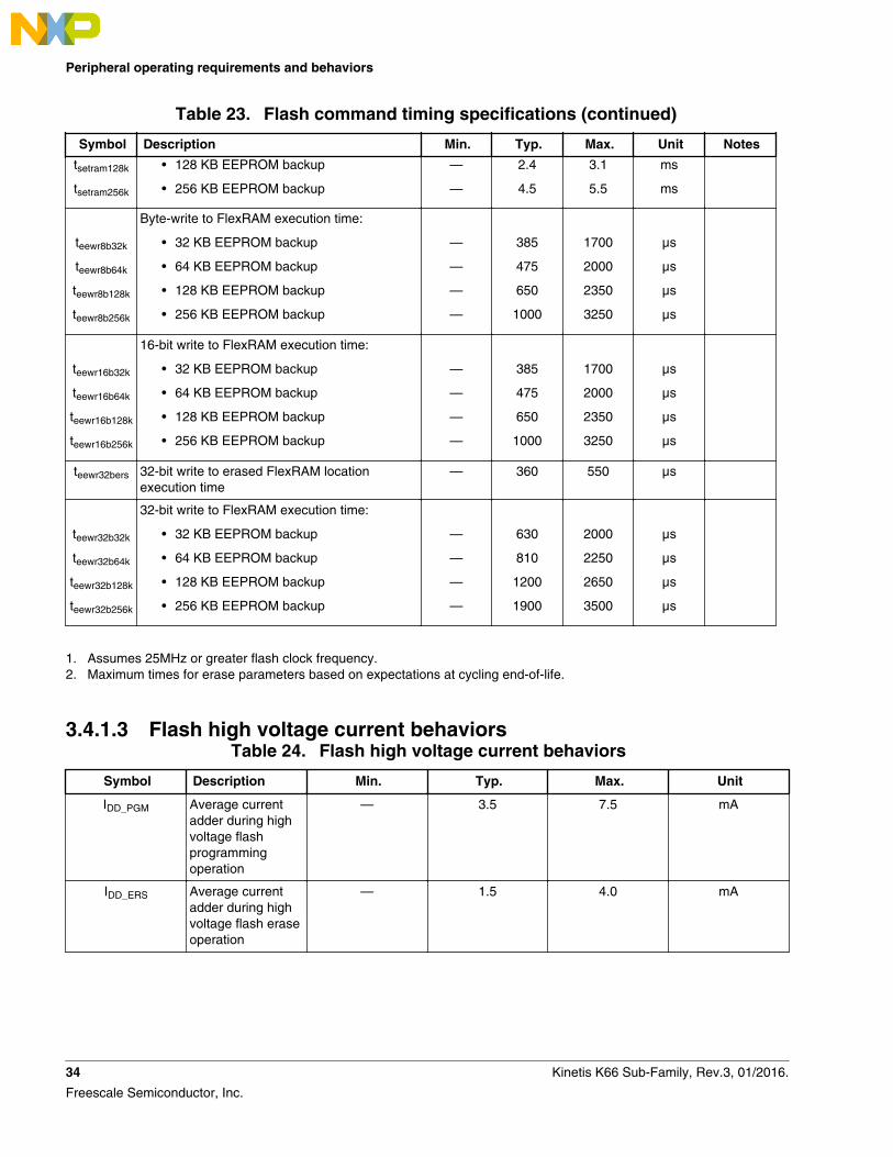
Table 23. Flash command timing specifications (continued)
Symbol Description Min. Typ. Max. Unit Notes
tsetram128k
tsetram256k
• 128 KB EEPROM backup
• 256 KB EEPROM backup
—
—
2.4
4.5
3.1
5.5
ms
ms
teewr8b32k
teewr8b64k
teewr8b128k
teewr8b256k
Byte-write to FlexRAM execution time:
• 32 KB EEPROM backup
• 64 KB EEPROM backup
• 128 KB EEPROM backup
• 256 KB EEPROM backup
—
—
—
—
385
475
650
1000
1700
2000
2350
3250
μs
μs
μs
μs
teewr16b32k
teewr16b64k
teewr16b128k
teewr16b256k
16-bit write to FlexRAM execution time:
• 32 KB EEPROM backup
• 64 KB EEPROM backup
• 128 KB EEPROM backup
• 256 KB EEPROM backup
—
—
—
—
385
475
650
1000
1700
2000
2350
3250
μs
μs
μs
μs
teewr32bers 32-bit write to erased FlexRAM locationexecution time
— 360 550 μs
teewr32b32k
teewr32b64k
teewr32b128k
teewr32b256k
32-bit write to FlexRAM execution time:
• 32 KB EEPROM backup
• 64 KB EEPROM backup
• 128 KB EEPROM backup
• 256 KB EEPROM backup
—
—
—
—
630
810
1200
1900
2000
2250
2650
3500
μs
μs
μs
μs
1. Assumes 25MHz or greater flash clock frequency.2. Maximum times for erase parameters based on expectations at cycling end-of-life.
3.4.1.3 Flash high voltage current behaviorsTable 24. Flash high voltage current behaviors
Symbol Description Min. Typ. Max. Unit
IDD_PGM Average currentadder during highvoltage flashprogrammingoperation
— 3.5 7.5 mA
IDD_ERS Average currentadder during highvoltage flash eraseoperation
— 1.5 4.0 mA
Peripheral operating requirements and behaviors
34 Kinetis K66 Sub-Family, Rev.3, 01/2016.
Freescale Semiconductor, Inc.
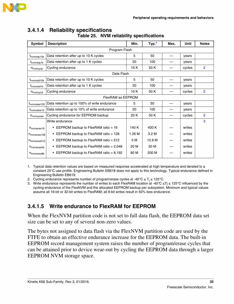
3.4.1.4 Reliability specificationsTable 25. NVM reliability specifications
Symbol Description Min. Typ.1 Max. Unit Notes
Program Flash
tnvmretp10k Data retention after up to 10 K cycles 5 50 — years
tnvmretp1k Data retention after up to 1 K cycles 20 100 — years
nnvmcycp Cycling endurance 10 K 50 K — cycles 2
Data Flash
tnvmretd10k Data retention after up to 10 K cycles 5 50 — years
tnvmretd1k Data retention after up to 1 K cycles 20 100 — years
nnvmcycd Cycling endurance 10 K 50 K — cycles 2
FlexRAM as EEPROM
tnvmretee100 Data retention up to 100% of write endurance 5 50 — years
tnvmretee10 Data retention up to 10% of write endurance 20 100 — years
nnvmcycee Cycling endurance for EEPROM backup 20 K 50 K — cycles 2
nnvmwree16
nnvmwree128
nnvmwree512
nnvmwree2k
nnvmwree8k
Write endurance
• EEPROM backup to FlexRAM ratio = 16
• EEPROM backup to FlexRAM ratio = 128
• EEPROM backup to FlexRAM ratio = 512
• EEPROM backup to FlexRAM ratio = 2,048
• EEPROM backup to FlexRAM ratio = 8,192
140 K
1.26 M
5 M
20 M
80 M
400 K
3.2 M
12.8 M
50 M
200 M
—
—
—
—
—
writes
writes
writes
writes
writes
3
1. Typical data retention values are based on measured response accelerated at high temperature and derated to aconstant 25°C use profile. Engineering Bulletin EB618 does not apply to this technology. Typical endurance defined inEngineering Bulletin EB619.
2. Cycling endurance represents number of program/erase cycles at -40°C ≤ Tj ≤ 125°C.3. Write endurance represents the number of writes to each FlexRAM location at -40°C ≤Tj ≤ 125°C influenced by the
cycling endurance of the FlexNVM and the allocated EEPROM backup per subsystem. Minimum and typical valuesassume all 16-bit or 32-bit writes to FlexRAM; all 8-bit writes result in 50% less endurance.
3.4.1.5 Write endurance to FlexRAM for EEPROM
When the FlexNVM partition code is not set to full data flash, the EEPROM data setsize can be set to any of several non-zero values.
The bytes not assigned to data flash via the FlexNVM partition code are used by theFTFE to obtain an effective endurance increase for the EEPROM data. The built-inEEPROM record management system raises the number of program/erase cycles thatcan be attained prior to device wear-out by cycling the EEPROM data through a largerEEPROM NVM storage space.
Peripheral operating requirements and behaviors
Kinetis K66 Sub-Family, Rev.3, 01/2016. 35
Freescale Semiconductor, Inc.
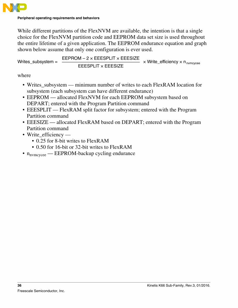
While different partitions of the FlexNVM are available, the intention is that a singlechoice for the FlexNVM partition code and EEPROM data set size is used throughoutthe entire lifetime of a given application. The EEPROM endurance equation and graphshown below assume that only one configuration is ever used.
Writes_subsystem = × Write_efficiency × nEEPROM – 2 × EEESPLIT × EEESIZE
EEESPLIT × EEESIZEnvmcycee
where
• Writes_subsystem — minimum number of writes to each FlexRAM location forsubsystem (each subsystem can have different endurance)
• EEPROM — allocated FlexNVM for each EEPROM subsystem based onDEPART; entered with the Program Partition command
• EEESPLIT — FlexRAM split factor for subsystem; entered with the ProgramPartition command
• EEESIZE — allocated FlexRAM based on DEPART; entered with the ProgramPartition command
• Write_efficiency —• 0.25 for 8-bit writes to FlexRAM• 0.50 for 16-bit or 32-bit writes to FlexRAM
• nnvmcycee — EEPROM-backup cycling endurance
Peripheral operating requirements and behaviors
36 Kinetis K66 Sub-Family, Rev.3, 01/2016.
Freescale Semiconductor, Inc.
16/32-bit
8-bit
Ratio of EEPROM Backup to FlexRAM
Aver
age
Writ
es p
er F
lexR
AM L
ocat
ion
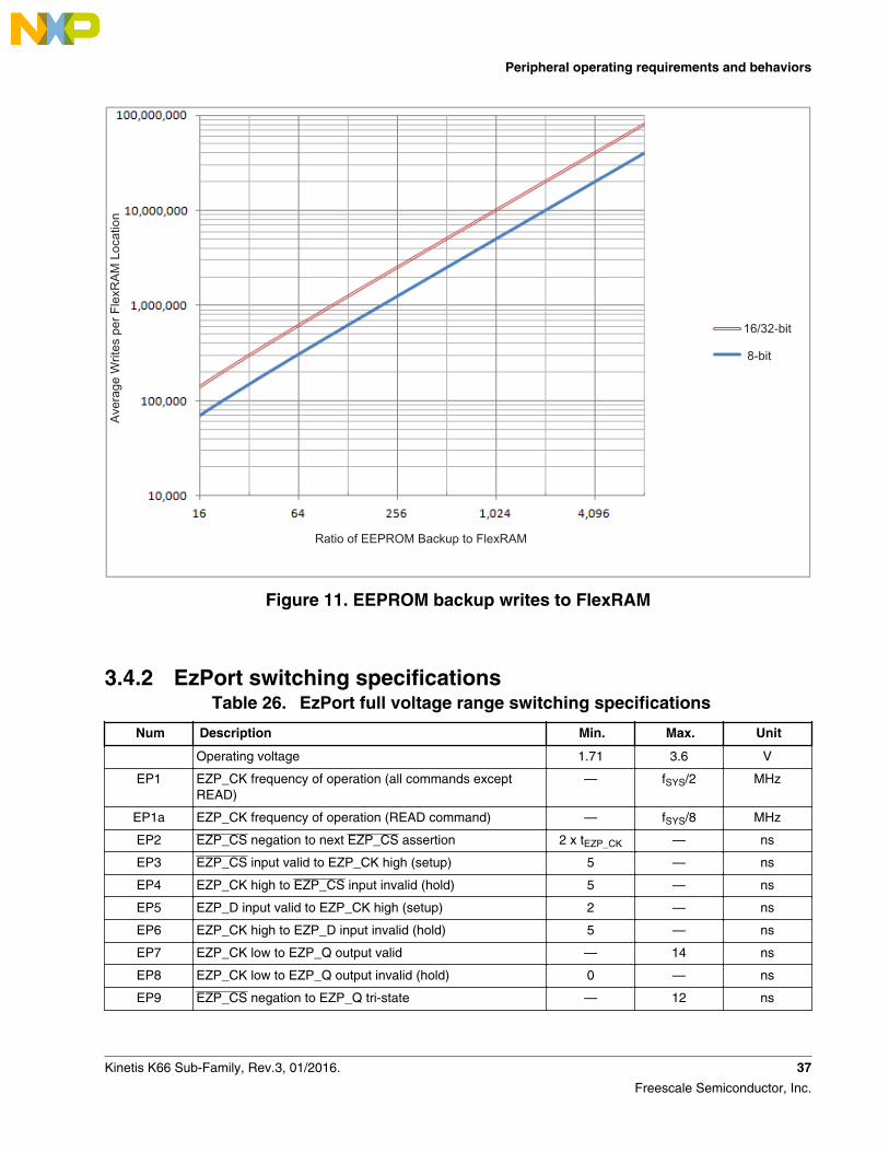
Figure 11. EEPROM backup writes to FlexRAM
3.4.2 EzPort switching specificationsTable 26. EzPort full voltage range switching specifications
Num Description Min. Max. Unit
Operating voltage 1.71 3.6 V
EP1 EZP_CK frequency of operation (all commands exceptREAD)
— fSYS/2 MHz
EP1a EZP_CK frequency of operation (READ command) — fSYS/8 MHz
EP2 EZP_CS negation to next EZP_CS assertion 2 x tEZP_CK — ns
EP3 EZP_CS input valid to EZP_CK high (setup) 5 — ns
EP4 EZP_CK high to EZP_CS input invalid (hold) 5 — ns
EP5 EZP_D input valid to EZP_CK high (setup) 2 — ns
EP6 EZP_CK high to EZP_D input invalid (hold) 5 — ns
EP7 EZP_CK low to EZP_Q output valid — 14 ns
EP8 EZP_CK low to EZP_Q output invalid (hold) 0 — ns
EP9 EZP_CS negation to EZP_Q tri-state — 12 ns
Peripheral operating requirements and behaviors
Kinetis K66 Sub-Family, Rev.3, 01/2016. 37
Freescale Semiconductor, Inc.
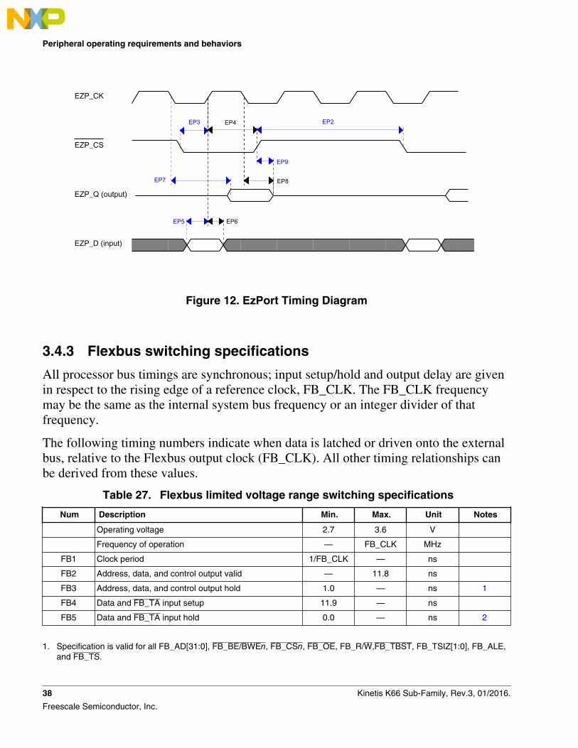
EP2EP3 EP4
EP5 EP6
EP7 EP8
EP9
EZP_CK
EZP_CS
EZP_Q (output)
EZP_D (input)
Figure 12. EzPort Timing Diagram
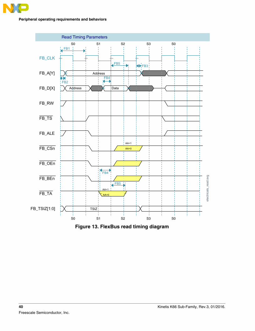
3.4.3 Flexbus switching specifications
All processor bus timings are synchronous; input setup/hold and output delay are givenin respect to the rising edge of a reference clock, FB_CLK. The FB_CLK frequencymay be the same as the internal system bus frequency or an integer divider of thatfrequency.
The following timing numbers indicate when data is latched or driven onto the externalbus, relative to the Flexbus output clock (FB_CLK). All other timing relationships canbe derived from these values.
Table 27. Flexbus limited voltage range switching specifications
Num Description Min. Max. Unit Notes
Operating voltage 2.7 3.6 V
Frequency of operation — FB_CLK MHz
FB1 Clock period 1/FB_CLK — ns
FB2 Address, data, and control output valid — 11.8 ns
FB3 Address, data, and control output hold 1.0 — ns 1
FB4 Data and FB_TA input setup 11.9 — ns
FB5 Data and FB_TA input hold 0.0 — ns 2
1. Specification is valid for all FB_AD[31:0], FB_BE/BWEn, FB_CSn, FB_OE, FB_R/W,FB_TBST, FB_TSIZ[1:0], FB_ALE,and FB_TS.
Peripheral operating requirements and behaviors
38 Kinetis K66 Sub-Family, Rev.3, 01/2016.
Freescale Semiconductor, Inc.

2. Specification is valid for all FB_AD[31:0] and FB_TA.
Table 28. Flexbus full voltage range switching specifications
Num Description Min. Max. Unit Notes
Operating voltage 1.71 3.6 V
Frequency of operation — FB_CLK MHz
FB1 Clock period 1/FB_CLK — ns
FB2 Address, data, and control output valid — 12.6 ns
FB3 Address, data, and control output hold 1.0 — ns 1
FB4 Data and FB_TA input setup 12.5 — ns
FB5 Data and FB_TA input hold 0 — ns 2
1. Specification is valid for all FB_AD[31:0], FB_BE/BWEn, FB_CSn, FB_OE, FB_R/W,FB_TBST, FB_TSIZ[1:0],FB_ALE, and FB_TS.
2. Specification is valid for all FB_AD[31:0] and FB_TA.
Peripheral operating requirements and behaviors
Kinetis K66 Sub-Family, Rev.3, 01/2016. 39
Freescale Semiconductor, Inc.
Address
Address Data
TSIZ
AA=1
AA=0
AA=1
AA=0
FB3FB5
FB4
FB4
FB5
FB1
FB_CLK
FB_A[Y]
FB_D[X]
FB_RW
FB_TS
FB_ALE
FB_CSn
FB_OEn
FB_BEn
FB_TA
FB_TSIZ[1:0]
FB2
Read Timing Parameters
elec
tric
als_
read
.svg
S0 S1 S2 S3 S0
S0 S1 S2 S3 S0
Figure 13. FlexBus read timing diagram
Peripheral operating requirements and behaviors
40 Kinetis K66 Sub-Family, Rev.3, 01/2016.
Freescale Semiconductor, Inc.
Address
Address Data
TSIZ
AA=1
AA=0
AA=1
AA=0
FB1
FB3
FB4
FB5
FB2FB_CLK
FB_A[Y]
FB_D[X]
FB_RW
FB_TS
FB_ALE
FB_CSn
FB_OEn
FB_BEn
FB_TA
FB_TSIZ[1:0]
Write Timing Parameters
elec
tric
als_
writ
e.sv
g
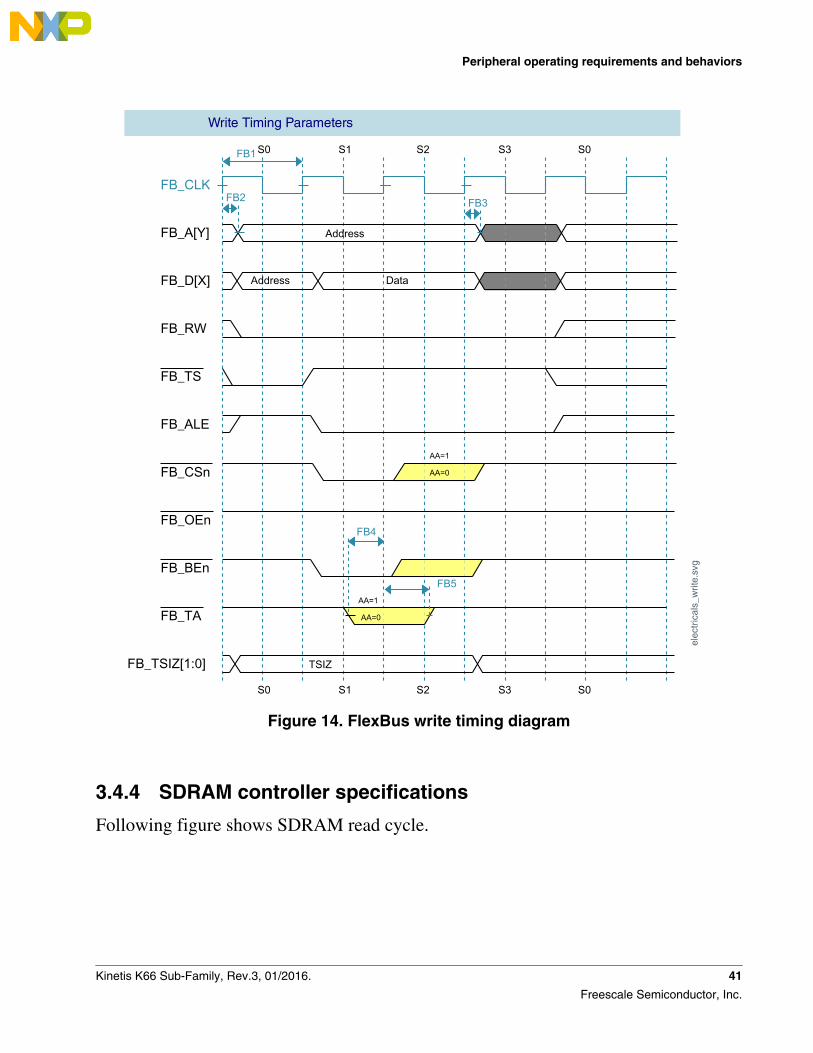
Figure 14. FlexBus write timing diagram
3.4.4 SDRAM controller specifications
Following figure shows SDRAM read cycle.
Peripheral operating requirements and behaviors
Kinetis K66 Sub-Family, Rev.3, 01/2016. 41
Freescale Semiconductor, Inc.
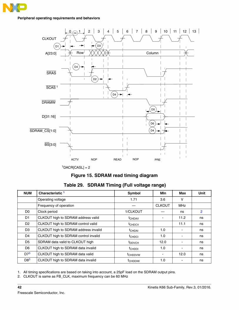
A[23:0]
SRAS
D[31:16]
ACTV NOP
SDRAM_CS[1:0]
READ
Column
CLKOUT
0
DRAMW
BS[3:0]
1 2 3 4 5 6 7 8 9 10 11 12 13
D1
D2
D4
D6
D5
D4
1
1
NOP
D4
Row
D3
PRE
D0
SCAS
DACR[CASL] = 2
Figure 15. SDRAM read timing diagram
Table 29. SDRAM Timing (Full voltage range)
NUM Characteristic 1 Symbol MIn Max Unit
Operating voltage 1.71 3.6 V
Frequency of operation — CLKOUT MHz
D0 Clock period 1/CLKOUT — ns 2
D1 CLKOUT high to SDRAM address valid tCHDAV - 11.2 ns
D2 CLKOUT high to SDRAM control valid tCHDCV 11.1 ns
D3 CLKOUT high to SDRAM address invalid tCHDAI 1.0 - ns
D4 CLKOUT high to SDRAM control invalid tCHDCI 1.0 - ns
D5 SDRAM data valid to CLKOUT high tDDVCH 12.0 - ns
D6 CLKOUT high to SDRAM data invalid tCHDDI 1.0 - ns
D73 CLKOUT high to SDRAM data valid tCHDDVW - 12.0 ns
D83 CLKOUT high to SDRAM data invalid tCHDDIW 1.0 - ns
1. All timing specifications are based on taking into account, a 25pF load on the SDRAM output pins.2. CLKOUT is same as FB_CLK, maximum frequency can be 60 MHz
Peripheral operating requirements and behaviors
42 Kinetis K66 Sub-Family, Rev.3, 01/2016.
Freescale Semiconductor, Inc.
3. D7 and D8 are for write cycles only.
Table 30. SDRAM Timing (Limited voltage range)
NUM Characteristic 1 Symbol MIn Max Unit
Operating voltage 2.7 3.6 V
Frequency of operation — CLKOUT MHz
D0 Clock period 1/CLKOUT — ns 2
D1 CLKOUT high to SDRAM address valid tCHDAV - 11.1 ns
D2 CLKOUT high to SDRAM control valid tCHDCV 11.1 ns
D3 CLKOUT high to SDRAM address invalid tCHDAI 1.0 - ns
D4 CLKOUT high to SDRAM control invalid tCHDCI 1.0 - ns
D5 SDRAM data valid to CLKOUT high tDDVCH 11.3 - ns
D6 CLKOUT high to SDRAM data invalid tCHDDI 1.0 - ns
D73 CLKOUT high to SDRAM data valid tCHDDVW - 11.1 ns
D83 CLKOUT high to SDRAM data invalid tCHDDIW 1.0 - ns
1. All timing specifications are based on taking into account, a 25pF load on the SDRAM output pins.2. CLKOUT is same as FB_CLK, maximum frequency can be 60 MHz3. D7 and D8 are for write cycles only.
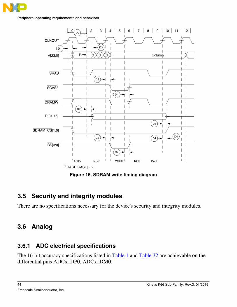
Following figure shows an SDRAM write cycle.
Peripheral operating requirements and behaviors
Kinetis K66 Sub-Family, Rev.3, 01/2016. 43
Freescale Semiconductor, Inc.
A[23:0]
SRAS
SCAS1
D[31:16]
ACTV PALLNOP
SDRAM_CS[1:0]
WRITE
Row Column
CLKOUT
DRAMW
BS[3:0]
D1
D2
D4
D8
D4
0 1 2 3 4 5 6 7 8 9 10 11 12
D7
NOP
1 DACR[CASL] = 2
D4
D3
D2
D4
D0
Figure 16. SDRAM write timing diagram
3.5 Security and integrity modules
There are no specifications necessary for the device's security and integrity modules.
3.6 Analog
3.6.1 ADC electrical specifications
The 16-bit accuracy specifications listed in Table 1 and Table 32 are achievable on thedifferential pins ADCx_DP0, ADCx_DM0.
Peripheral operating requirements and behaviors
44 Kinetis K66 Sub-Family, Rev.3, 01/2016.
Freescale Semiconductor, Inc.
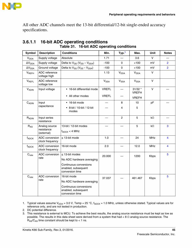
All other ADC channels meet the 13-bit differential/12-bit single-ended accuracyspecifications.
3.6.1.1 16-bit ADC operating conditionsTable 31. 16-bit ADC operating conditions
Symbol Description Conditions Min. Typ.1 Max. Unit Notes
VDDA Supply voltage Absolute 1.71 — 3.6 V —
ΔVDDA Supply voltage Delta to VDD (VDD – VDDA) -100 0 +100 mV 2
ΔVSSA Ground voltage Delta to VSS (VSS – VSSA) -100 0 +100 mV 2
VREFH ADC referencevoltage high
1.13 VDDA VDDA V
VREFL ADC referencevoltage low
VSSA VSSA VSSA V
VADIN Input voltage • 16-bit differential mode
• All other modes
VREFL
VREFL
—
—
31/32 *VREFH
VREFH
V —
CADIN Inputcapacitance
• 16-bit mode
• 8-bit / 10-bit / 12-bitmodes
—
—
8
4
10
5
pF —
RADIN Input seriesresistance
— 2 5 kΩ —
RAS Analog sourceresistance(external)
13-bit / 12-bit modes
fADCK < 4 MHz
— — 5 kΩ 3
fADCK ADC conversionclock frequency
≤ 13-bit mode 1.0 — 24 MHz 4
fADCK ADC conversionclock frequency
16-bit mode 2.0 — 12.0 MHz 4
Crate ADC conversionrate
≤ 13-bit modes
No ADC hardware averaging
Continuous conversionsenabled, subsequentconversion time
20.000 — 1200 Kbps5
Crate ADC conversionrate
16-bit mode
No ADC hardware averaging
Continuous conversionsenabled, subsequentconversion time
37.037 — 461.467 Kbps5
1. Typical values assume VDDA = 3.0 V, Temp = 25 °C, fADCK = 1.0 MHz, unless otherwise stated. Typical values are forreference only, and are not tested in production.
2. DC potential difference.3. This resistance is external to MCU. To achieve the best results, the analog source resistance must be kept as low as
possible. The results in this data sheet were derived from a system that had < 8 Ω analog source resistance. TheRAS/CAS time constant should be kept to < 1 ns.
Peripheral operating requirements and behaviors
Kinetis K66 Sub-Family, Rev.3, 01/2016. 45
Freescale Semiconductor, Inc.
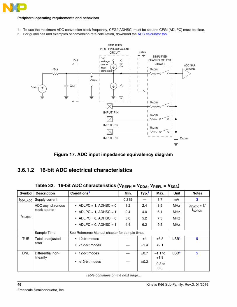
4. To use the maximum ADC conversion clock frequency, CFG2[ADHSC] must be set and CFG1[ADLPC] must be clear.5. For guidelines and examples of conversion rate calculation, download the ADC calculator tool.
RAS
VAS CAS
ZAS
VADIN
ZADIN
RADIN
RADIN
RADIN
RADIN
CADIN
Pad leakagedue toinput protection
INPUT PIN
INPUT PIN
INPUT PIN
SIMPLIFIEDINPUT PIN EQUIVALENT
CIRCUITSIMPLIFIED
CHANNEL SELECTCIRCUIT ADC SAR
ENGINE
Figure 17. ADC input impedance equivalency diagram
3.6.1.2 16-bit ADC electrical characteristics
Table 32. 16-bit ADC characteristics (VREFH = VDDA, VREFL = VSSA)
Symbol Description Conditions1 Min. Typ.2 Max. Unit Notes
IDDA_ADC Supply current 0.215 — 1.7 mA 3
fADACK
ADC asynchronousclock source
• ADLPC = 1, ADHSC = 0
• ADLPC = 1, ADHSC = 1
• ADLPC = 0, ADHSC = 0
• ADLPC = 0, ADHSC = 1
1.2
2.4
3.0
4.4
2.4
4.0
5.2
6.2
3.9
6.1
7.3
9.5
MHz
MHz
MHz
MHz
tADACK = 1/fADACK
Sample Time See Reference Manual chapter for sample times
TUE Total unadjustederror
• 12-bit modes
• <12-bit modes
—
—
±4
±1.4
±6.8
±2.1
LSB4 5
DNL Differential non-linearity
• 12-bit modes
• <12-bit modes
—
—
±0.7
±0.2
–1.1 to+1.9
–0.3 to0.5
LSB4 5
Table continues on the next page...
Peripheral operating requirements and behaviors
46 Kinetis K66 Sub-Family, Rev.3, 01/2016.
Freescale Semiconductor, Inc.
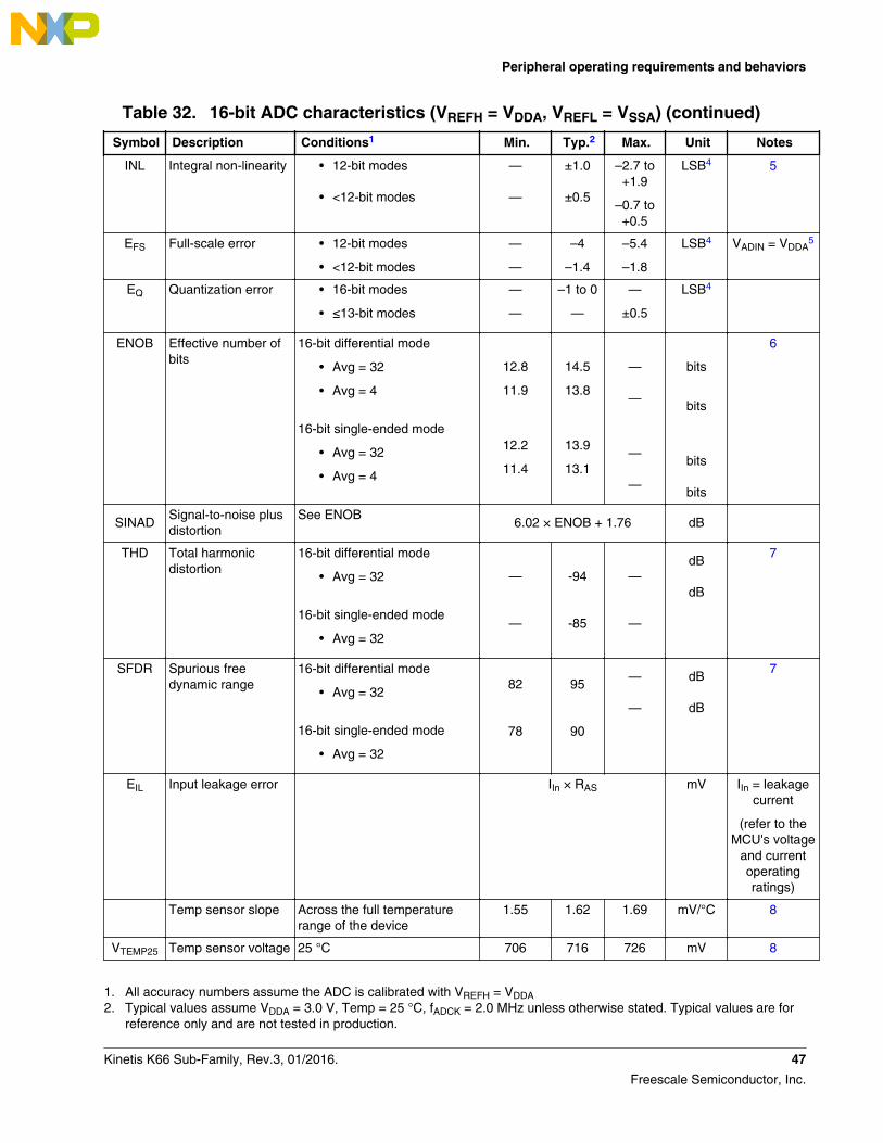
Table 32. 16-bit ADC characteristics (VREFH = VDDA, VREFL = VSSA) (continued)
Symbol Description Conditions1 Min. Typ.2 Max. Unit Notes
INL Integral non-linearity • 12-bit modes
• <12-bit modes
—
—
±1.0
±0.5
–2.7 to+1.9
–0.7 to+0.5
LSB4 5
EFS Full-scale error • 12-bit modes
• <12-bit modes
—
—
–4
–1.4
–5.4
–1.8
LSB4 VADIN = VDDA5
EQ Quantization error • 16-bit modes
• ≤13-bit modes
—
—
–1 to 0
—
—
±0.5
LSB4
ENOB Effective number ofbits
16-bit differential mode
• Avg = 32
• Avg = 4
16-bit single-ended mode
• Avg = 32
• Avg = 4
12.8
11.9
12.2
11.4
14.5
13.8
13.9
13.1
—
—
—
—
bits
bits
bits
bits
6
SINADSignal-to-noise plusdistortion
See ENOB6.02 × ENOB + 1.76 dB
THD Total harmonicdistortion
16-bit differential mode
• Avg = 32
16-bit single-ended mode
• Avg = 32
—
—
-94
-85
—
—
dB
dB
7
SFDR Spurious freedynamic range
16-bit differential mode
• Avg = 32
16-bit single-ended mode
• Avg = 32
82
78
95
90
—
—
dB
dB
7
EIL Input leakage error IIn × RAS mV IIn = leakagecurrent
(refer to theMCU's voltage
and currentoperatingratings)
Temp sensor slope Across the full temperaturerange of the device
1.55 1.62 1.69 mV/°C 8
VTEMP25 Temp sensor voltage 25 °C 706 716 726 mV 8
1. All accuracy numbers assume the ADC is calibrated with VREFH = VDDA2. Typical values assume VDDA = 3.0 V, Temp = 25 °C, fADCK = 2.0 MHz unless otherwise stated. Typical values are for
reference only and are not tested in production.
Peripheral operating requirements and behaviors
Kinetis K66 Sub-Family, Rev.3, 01/2016. 47
Freescale Semiconductor, Inc.
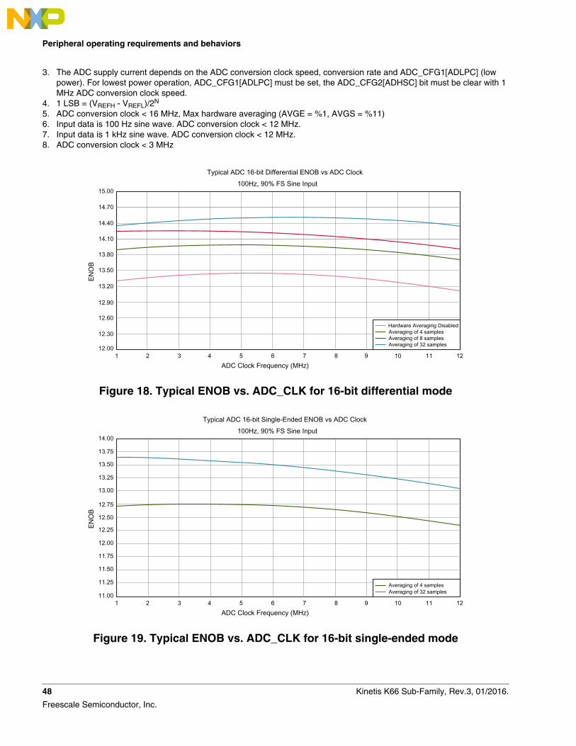
3. The ADC supply current depends on the ADC conversion clock speed, conversion rate and ADC_CFG1[ADLPC] (lowpower). For lowest power operation, ADC_CFG1[ADLPC] must be set, the ADC_CFG2[ADHSC] bit must be clear with 1MHz ADC conversion clock speed.
4. 1 LSB = (VREFH - VREFL)/2N
5. ADC conversion clock < 16 MHz, Max hardware averaging (AVGE = %1, AVGS = %11)6. Input data is 100 Hz sine wave. ADC conversion clock < 12 MHz.7. Input data is 1 kHz sine wave. ADC conversion clock < 12 MHz.8. ADC conversion clock < 3 MHz
Typical ADC 16-bit Differential ENOB vs ADC Clock100Hz, 90% FS Sine Input
ENO
B
ADC Clock Frequency (MHz)
15.00
14.70
14.40
14.10
13.80
13.50
13.20
12.90
12.60
12.30
12.001 2 3 4 5 6 7 8 9 10 1211
Hardware Averaging DisabledAveraging of 4 samplesAveraging of 8 samplesAveraging of 32 samples
Figure 18. Typical ENOB vs. ADC_CLK for 16-bit differential mode
Typical ADC 16-bit Single-Ended ENOB vs ADC Clock100Hz, 90% FS Sine Input
ENO
B
ADC Clock Frequency (MHz)
14.00
13.75
13.25
13.00
12.75
12.50
12.00
11.75
11.50
11.25
11.001 2 3 4 5 6 7 8 9 10 1211
Averaging of 4 samplesAveraging of 32 samples
13.50
12.25
Figure 19. Typical ENOB vs. ADC_CLK for 16-bit single-ended mode
Peripheral operating requirements and behaviors
48 Kinetis K66 Sub-Family, Rev.3, 01/2016.
Freescale Semiconductor, Inc.
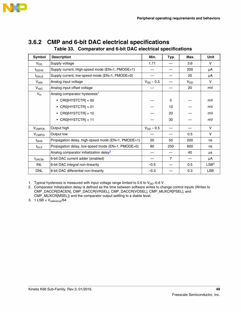
3.6.2 CMP and 6-bit DAC electrical specificationsTable 33. Comparator and 6-bit DAC electrical specifications
Symbol Description Min. Typ. Max. Unit
VDD Supply voltage 1.71 — 3.6 V
IDDHS Supply current, High-speed mode (EN=1, PMODE=1) — — 200 μA
IDDLS Supply current, low-speed mode (EN=1, PMODE=0) — — 20 μA
VAIN Analog input voltage VSS – 0.3 — VDD V
VAIO Analog input offset voltage — — 20 mV
VH Analog comparator hysteresis1
• CR0[HYSTCTR] = 00
• CR0[HYSTCTR] = 01
• CR0[HYSTCTR] = 10
• CR0[HYSTCTR] = 11
—
—
—
—
5
10
20
30
—
—
—
—
mV
mV
mV
mV
VCMPOh Output high VDD – 0.5 — — V
VCMPOl Output low — — 0.5 V
tDHS Propagation delay, high-speed mode (EN=1, PMODE=1) 20 50 200 ns
tDLS Propagation delay, low-speed mode (EN=1, PMODE=0) 80 250 600 ns
Analog comparator initialization delay2 — — 40 μs
IDAC6b 6-bit DAC current adder (enabled) — 7 — μA
INL 6-bit DAC integral non-linearity –0.5 — 0.5 LSB3
DNL 6-bit DAC differential non-linearity –0.3 — 0.3 LSB
1. Typical hysteresis is measured with input voltage range limited to 0.6 to VDD–0.6 V.2. Comparator initialization delay is defined as the time between software writes to change control inputs (Writes to
CMP_DACCR[DACEN], CMP_DACCR[VRSEL], CMP_DACCR[VOSEL], CMP_MUXCR[PSEL], andCMP_MUXCR[MSEL]) and the comparator output settling to a stable level.
3. 1 LSB = Vreference/64
Peripheral operating requirements and behaviors
Kinetis K66 Sub-Family, Rev.3, 01/2016. 49
Freescale Semiconductor, Inc.
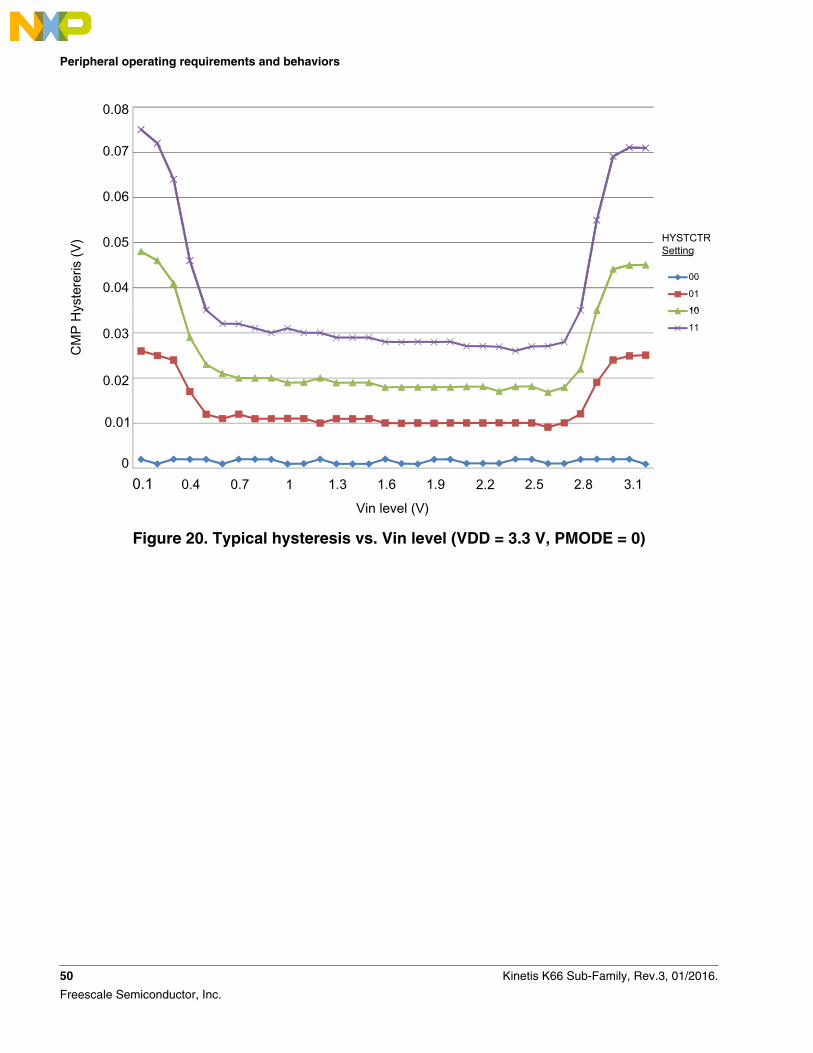
00
01
10
HYSTCTR Setting
0.1
10
11
Vin level (V)
CM
P H
yste
reris
(V)
3.12.82.52.21.91.61.310.70.4
0.05
0
0.01
0.02
0.03
0.08
0.07
0.06
0.04
Figure 20. Typical hysteresis vs. Vin level (VDD = 3.3 V, PMODE = 0)
Peripheral operating requirements and behaviors
50 Kinetis K66 Sub-Family, Rev.3, 01/2016.
Freescale Semiconductor, Inc.
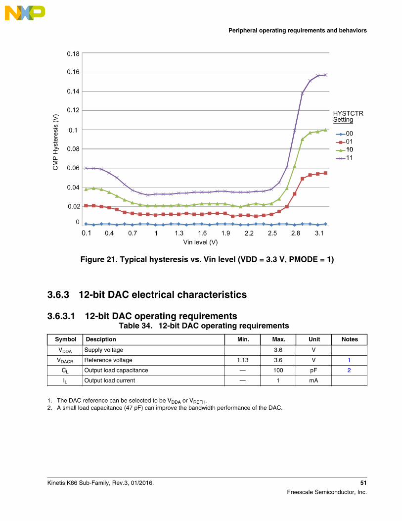
000110
HYSTCTR Setting
1011
0.1 3.12.82.52.21.91.61.310.70.4
0.1
0
0.02
0.04
0.06
0.18
0.14
0.12
0.08
0.16
Vin level (V)
CM
P H
yste
resi
s (V
)
Figure 21. Typical hysteresis vs. Vin level (VDD = 3.3 V, PMODE = 1)
3.6.3 12-bit DAC electrical characteristics
3.6.3.1 12-bit DAC operating requirementsTable 34. 12-bit DAC operating requirements
Symbol Desciption Min. Max. Unit Notes
VDDA Supply voltage 3.6 V
VDACR Reference voltage 1.13 3.6 V 1
CL Output load capacitance — 100 pF 2
IL Output load current — 1 mA
1. The DAC reference can be selected to be VDDA or VREFH.2. A small load capacitance (47 pF) can improve the bandwidth performance of the DAC.
Peripheral operating requirements and behaviors
Kinetis K66 Sub-Family, Rev.3, 01/2016. 51
Freescale Semiconductor, Inc.
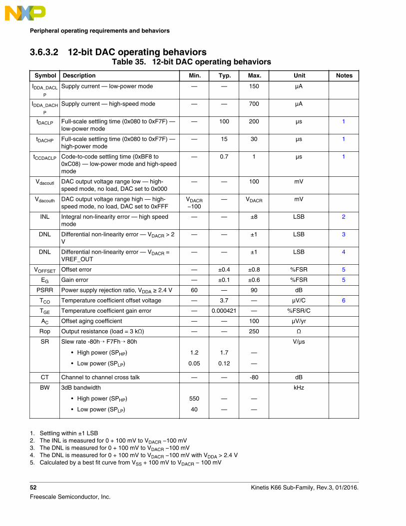
3.6.3.2 12-bit DAC operating behaviorsTable 35. 12-bit DAC operating behaviors
Symbol Description Min. Typ. Max. Unit Notes
IDDA_DACL
P
Supply current — low-power mode — — 150 μA
IDDA_DACH
P
Supply current — high-speed mode — — 700 μA
tDACLP Full-scale settling time (0x080 to 0xF7F) —low-power mode
— 100 200 μs 1
tDACHP Full-scale settling time (0x080 to 0xF7F) —high-power mode
— 15 30 μs 1
tCCDACLP Code-to-code settling time (0xBF8 to0xC08) — low-power mode and high-speedmode
— 0.7 1 μs 1
Vdacoutl DAC output voltage range low — high-speed mode, no load, DAC set to 0x000
— — 100 mV
Vdacouth DAC output voltage range high — high-speed mode, no load, DAC set to 0xFFF
VDACR−100
— VDACR mV
INL Integral non-linearity error — high speedmode
— — ±8 LSB 2
DNL Differential non-linearity error — VDACR > 2V
— — ±1 LSB 3
DNL Differential non-linearity error — VDACR =VREF_OUT
— — ±1 LSB 4
VOFFSET Offset error — ±0.4 ±0.8 %FSR 5
EG Gain error — ±0.1 ±0.6 %FSR 5
PSRR Power supply rejection ratio, VDDA ≥ 2.4 V 60 — 90 dB
TCO Temperature coefficient offset voltage — 3.7 — μV/C 6
TGE Temperature coefficient gain error — 0.000421 — %FSR/C
AC Offset aging coefficient — — 100 μV/yr
Rop Output resistance (load = 3 kΩ) — — 250 Ω
SR Slew rate -80h→ F7Fh→ 80h
• High power (SPHP)
• Low power (SPLP)
1.2
0.05
1.7
0.12
—
—
V/μs
CT Channel to channel cross talk — — -80 dB
BW 3dB bandwidth
• High power (SPHP)
• Low power (SPLP)
550
40
—
—
—
—
kHz
1. Settling within ±1 LSB2. The INL is measured for 0 + 100 mV to VDACR −100 mV3. The DNL is measured for 0 + 100 mV to VDACR −100 mV4. The DNL is measured for 0 + 100 mV to VDACR −100 mV with VDDA > 2.4 V5. Calculated by a best fit curve from VSS + 100 mV to VDACR − 100 mV
Peripheral operating requirements and behaviors
52 Kinetis K66 Sub-Family, Rev.3, 01/2016.
Freescale Semiconductor, Inc.
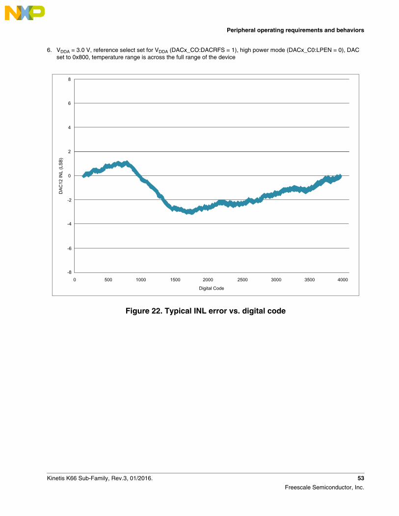
6. VDDA = 3.0 V, reference select set for VDDA (DACx_CO:DACRFS = 1), high power mode (DACx_C0:LPEN = 0), DACset to 0x800, temperature range is across the full range of the device
Digital Code
DAC
12 IN
L (L
SB)
0
500 1000 1500 2000 2500 3000 3500 4000
2
4
6
8
-2
-4
-6
-80
Figure 22. Typical INL error vs. digital code
Peripheral operating requirements and behaviors
Kinetis K66 Sub-Family, Rev.3, 01/2016. 53
Freescale Semiconductor, Inc.
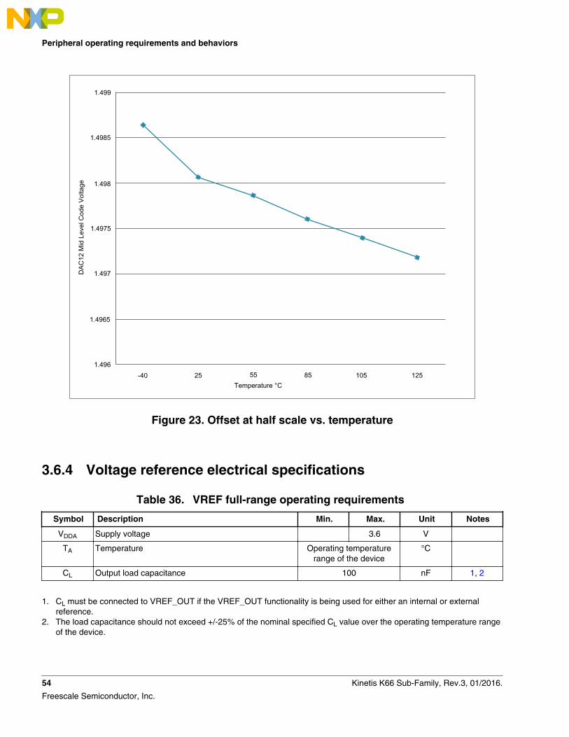
Temperature °C
DAC
12 M
id L
evel
Cod
e Vo
ltage
25 55 85 105 125
1.499
-40
1.4985
1.498
1.4975
1.497
1.4965
1.496
Figure 23. Offset at half scale vs. temperature
3.6.4 Voltage reference electrical specifications
Table 36. VREF full-range operating requirements
Symbol Description Min. Max. Unit Notes
VDDA Supply voltage 3.6 V
TA Temperature Operating temperaturerange of the device
°C
CL Output load capacitance 100 nF 1, 2
1. CL must be connected to VREF_OUT if the VREF_OUT functionality is being used for either an internal or externalreference.
2. The load capacitance should not exceed +/-25% of the nominal specified CL value over the operating temperature rangeof the device.
Peripheral operating requirements and behaviors
54 Kinetis K66 Sub-Family, Rev.3, 01/2016.
Freescale Semiconductor, Inc.

Table 37. VREF full-range operating behaviors
Symbol Description Min. Typ. Max. Unit Notes
Vout Voltage reference output with factory trim atnominal VDDA and temperature=25C
1.1915 1.195 1.1977 V 1
Vout Voltage reference output — factory trim 1.1584 — 1.2376 V 1
Vout Voltage reference output — user trim 1.193 — 1.197 V 1
Vstep Voltage reference trim step — 0.5 — mV 1
Vtdrift Temperature drift (Vmax -Vmin across the fulltemperature range)
— — 80 mV 1
Ac Aging coefficient — — 400 uV/yr —
Ibg Bandgap only current — — 80 µA 1
ΔVLOAD Load regulation
• current = ± 1.0 mA
—
200
—
µV 1, 2
Tstup Buffer startup time — — 100 µs
Tchop_osc_st
up
Internal bandgap start-up delay with choposcillator enabled
— — 35 ms —
Vvdrift Voltage drift (Vmax -Vmin across the fullvoltage range)
— 2 — mV 1
1. See the chip's Reference Manual for the appropriate settings of the VREF Status and Control register.2. Load regulation voltage is the difference between the VREF_OUT voltage with no load vs. voltage with defined load
Table 38. VREF limited-range operating requirements
Symbol Description Min. Max. Unit Notes
TA Temperature 0 50 °C
Table 39. VREF limited-range operating behaviors
Symbol Description Min. Max. Unit Notes
Vout Voltage reference output with factory trim 1.173 1.225 V
3.7 Timers
See General switching specifications.
3.8 Communication interfaces
Peripheral operating requirements and behaviors
Kinetis K66 Sub-Family, Rev.3, 01/2016. 55
Freescale Semiconductor, Inc.
3.8.1 Ethernet switching specifications
The following timing specs are defined at the chip I/O pin and must be translatedappropriately to arrive at timing specs/constraints for the physical interface.
3.8.1.1 MII signal switching specifications
The following timing specs meet the requirements for MII style interfaces for a range oftransceiver devices.
Table 40. MII signal switching specifications
Symbol Description Min. Max. Unit
— Operating Voltage 2.7 3.6 V
— RXCLK frequency — 25 MHz
MII1 RXCLK pulse width high 35% 65% RXCLK
period
MII2 RXCLK pulse width low 35% 65% RXCLK
period
MII3 RXD[3:0], RXDV, RXER to RXCLK setup 5 — ns
MII4 RXCLK to RXD[3:0], RXDV, RXER hold 5 — ns
— TXCLK frequency — 25 MHz
MII5 TXCLK pulse width high 35% 65% TXCLK
period
MII6 TXCLK pulse width low 35% 65% TXCLK
period
MII7 TXCLK to TXD[3:0], TXEN, TXER invalid 2 — ns
MII8 TXCLK to TXD[3:0], TXEN, TXER valid — 25 ns
Peripheral operating requirements and behaviors
56 Kinetis K66 Sub-Family, Rev.3, 01/2016.
Freescale Semiconductor, Inc.
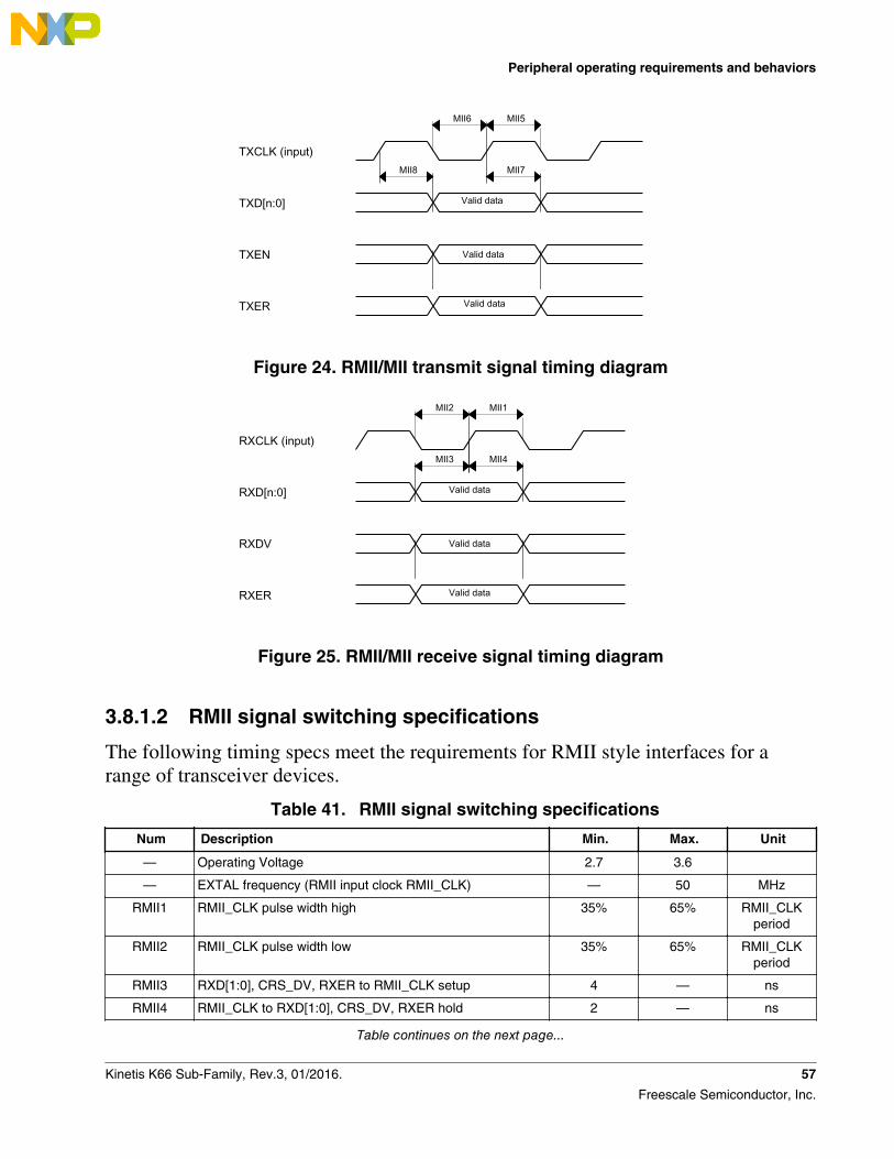
MII7MII8
Valid data
Valid data
Valid data
MII6 MII5
TXCLK (input)
TXD[n:0]
TXEN
TXER
Figure 24. RMII/MII transmit signal timing diagram
MII2 MII1
MII4MII3
Valid data
Valid data
Valid data
RXCLK (input)
RXD[n:0]
RXDV
RXER
Figure 25. RMII/MII receive signal timing diagram
3.8.1.2 RMII signal switching specifications
The following timing specs meet the requirements for RMII style interfaces for arange of transceiver devices.
Table 41. RMII signal switching specifications
Num Description Min. Max. Unit
— Operating Voltage 2.7 3.6
— EXTAL frequency (RMII input clock RMII_CLK) — 50 MHz
RMII1 RMII_CLK pulse width high 35% 65% RMII_CLKperiod
RMII2 RMII_CLK pulse width low 35% 65% RMII_CLKperiod
RMII3 RXD[1:0], CRS_DV, RXER to RMII_CLK setup 4 — ns
RMII4 RMII_CLK to RXD[1:0], CRS_DV, RXER hold 2 — ns
Table continues on the next page...
Peripheral operating requirements and behaviors
Kinetis K66 Sub-Family, Rev.3, 01/2016. 57
Freescale Semiconductor, Inc.
Table 41. RMII signal switching specifications(continued)
Num Description Min. Max. Unit
RMII7 RMII_CLK to TXD[1:0], TXEN invalid 4 — ns
RMII8 RMII_CLK to TXD[1:0], TXEN valid — 15.4 ns
3.8.2 USB Voltage Regulator Electrical SpecificationsTable 42. USB VREG electrical specifications
Symbol Description Min. Typ.1 Max. Unit Notes
VREG_IN0
VREG_IN1
Regulator selectable input supply voltages 2.7 — 5.5 V 2
IDDon
VREG_IN0
VREG_IN1
Quiescent current — Run mode, load currentequal zero, input supply (VREG_IN*) > 3.6 V —
—157
157
—
—
μA
IDDstby
VREG_IN0
VREG_IN1
Quiescent current — Standby mode, loadcurrent equal zero
—
—
2
2
—
—
μA
IDDoff
VREG_IN0
VREG_IN1
Quiescent current — Shutdown mode
• VREG_IN*= 5.0 V and temperature=25 °C —
—
680
920
—
—
nA
ILOADrun Maximum load current — Run mode — — 150 mA 3
ILOADstby Maximum load current — Standby mode — — 1 mA
VDROPOUT Regulator drop-out voltage — Run mode atmaximum load current with inrush current limitdisabled
300 — — mV
VREG_OUT Regulator programmable output target voltage— Selected input supply > programmed outputtarget voltage + VDROPOUT
• Run mode
• Standby mode
3
2.1
3.3
2.8
3.6
3.6
V
V
4
COUT External output capacitor 1.76 2.2 8.16 μF
ESR External output capacitor equivalent seriesresistance
1 — 100 mΩ
ILIM Short circuit current — 350 — mA 5
IINRUSH Inrush current limit 40 — 100 mA 6, 7, 8, 9, 10
1. Typical values assume the selected input supply is 5.0 V, Temp = 25 °C unless otherwise stated.
Peripheral operating requirements and behaviors
58 Kinetis K66 Sub-Family, Rev.3, 01/2016.
Freescale Semiconductor, Inc.
2. Operation range is 2.7 V to 5.5 V; tolerance voltage is up to 6 V.3. 150mA is inclusive of the run mode current of the on-chip USB modules. Available load outside of the chip depends on
USB operation and device power dissipation limits.4. The target voltage for the regulator is programmable, accounting for the range of the max and min values5. Current limit disabled.6. Current limit should be disabled after the powers have stabilized to allow full functionality of the regulator.7. Limited Characterization8. IINRUSH with VREGINx=4.0 V to 5.5 V9. The minimum value of IINRUSH is stated for operation when only one of VREG_IN0 / VREG_IN1 is powered, or when
VREG_IN0 and VREG_IN1 both have the same voltage level. When VREG_IN0 and VREG_IN1 are operated atdifferent voltage levels with the selected VREG_IN lower than the non-selected VREG_IN, the minumum value ofIINRUSH may decrease to a lower value.
10. Total current load on startup should be less than IINRUSH min over full input voltage range of the regulator.
3.8.3 USB Full Speed Transceiver and High Speed PHYspecifications
This section describes the USB0 port Full Speed/Low Speed transceiver and USB1port USB-PHY High Speed Phy parameters. The high speed phy is capable of full andlow speed signalling as well.
The USB0 (FS/LS Transceiver) and USB1 ((USB HS/FS/LS) meet the electricalcompliance requirements defined in the Universal Serial Bus Revision 2.0Specification with the amendments below.
• USB ENGINEERING CHANGE NOTICE• Title: 5V Short Circuit Withstand Requirement Change• Applies to: Universal Serial Bus Specification, Revision 2.0
• Errata for USB Revision 2.0 April 27, 2000 as of 12/7/2000• USB ENGINEERING CHANGE NOTICE
• Title: Pull-up/Pull-down resistors• Applies to: Universal Serial Bus Specification, Revision 2.0
• USB ENGINEERING CHANGE NOTICE• Title: Suspend Current Limit Changes• Applies to: Universal Serial Bus Specification, Revision 2.0
• On-The-Go and Embedded Host Supplement to the USB Revision 2.0Specification
• Revision 2.0 version 1.1a July 27, 2012• Battery Charging Specification (available from USB-IF)
• Revision 1.2 (including errata and ECNs through March 15, 2012), March 15,2012
USB1_VBUS pin is a detector function which is 5v tolerant and complies with theabove specifications without needing any external voltage division components.
Peripheral operating requirements and behaviors
Kinetis K66 Sub-Family, Rev.3, 01/2016. 59
Freescale Semiconductor, Inc.
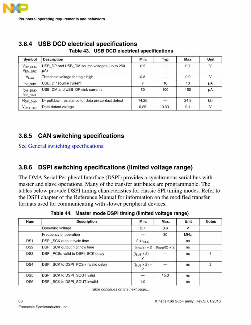
3.8.4 USB DCD electrical specificationsTable 43. USB DCD electrical specifications
Symbol Description Min. Typ. Max. Unit
VDP_SRC,VDM_SRC
USB_DP and USB_DM source voltages (up to 250μA)
0.5 — 0.7 V
VLGC Threshold voltage for logic high 0.8 — 2.0 V
IDP_SRC USB_DP source current 7 10 13 μA
IDM_SINK,IDP_SINK
USB_DM and USB_DP sink currents 50 100 150 μA
RDM_DWN D- pulldown resistance for data pin contact detect 14.25 — 24.8 kΩ
VDAT_REF Data detect voltage 0.25 0.33 0.4 V
3.8.5 CAN switching specifications
See General switching specifications.
3.8.6 DSPI switching specifications (limited voltage range)
The DMA Serial Peripheral Interface (DSPI) provides a synchronous serial bus withmaster and slave operations. Many of the transfer attributes are programmable. Thetables below provide DSPI timing characteristics for classic SPI timing modes. Refer tothe DSPI chapter of the Reference Manual for information on the modified transferformats used for communicating with slower peripheral devices.
Table 44. Master mode DSPI timing (limited voltage range)
Num Description Min. Max. Unit Notes
Operating voltage 2.7 3.6 V
Frequency of operation — 30 MHz
DS1 DSPI_SCK output cycle time 2 x tBUS — ns
DS2 DSPI_SCK output high/low time (tSCK/2) − 2 (tSCK/2) + 2 ns
DS3 DSPI_PCSn valid to DSPI_SCK delay (tBUS x 2) −2
— ns 1
DS4 DSPI_SCK to DSPI_PCSn invalid delay (tBUS x 2) −2
— ns 2
DS5 DSPI_SCK to DSPI_SOUT valid — 15.0 ns
DS6 DSPI_SCK to DSPI_SOUT invalid 1.0 — ns
Table continues on the next page...
Peripheral operating requirements and behaviors
60 Kinetis K66 Sub-Family, Rev.3, 01/2016.
Freescale Semiconductor, Inc.
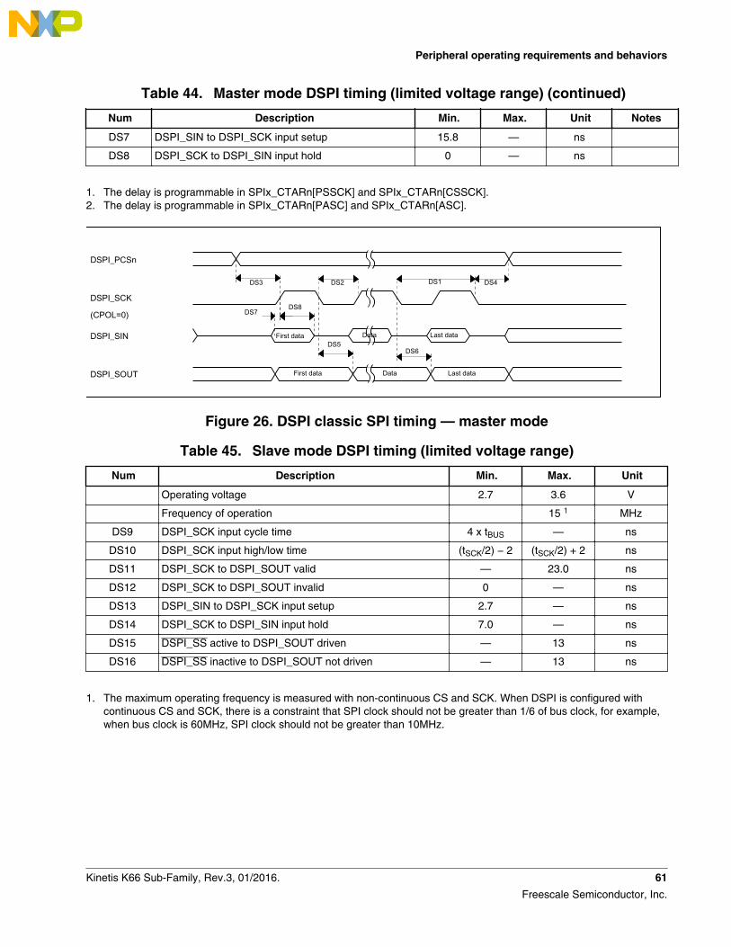
Table 44. Master mode DSPI timing (limited voltage range) (continued)
Num Description Min. Max. Unit Notes
DS7 DSPI_SIN to DSPI_SCK input setup 15.8 — ns
DS8 DSPI_SCK to DSPI_SIN input hold 0 — ns
1. The delay is programmable in SPIx_CTARn[PSSCK] and SPIx_CTARn[CSSCK].2. The delay is programmable in SPIx_CTARn[PASC] and SPIx_CTARn[ASC].
DS3 DS4DS1DS2
DS7DS8
First data Last dataDS5
First data Data Last data
DS6
Data
DSPI_PCSn
DSPI_SCK
(CPOL=0)
DSPI_SIN
DSPI_SOUT
Figure 26. DSPI classic SPI timing — master mode
Table 45. Slave mode DSPI timing (limited voltage range)
Num Description Min. Max. Unit
Operating voltage 2.7 3.6 V
Frequency of operation 15 1 MHz
DS9 DSPI_SCK input cycle time 4 x tBUS — ns
DS10 DSPI_SCK input high/low time (tSCK/2) − 2 (tSCK/2) + 2 ns
DS11 DSPI_SCK to DSPI_SOUT valid — 23.0 ns
DS12 DSPI_SCK to DSPI_SOUT invalid 0 — ns
DS13 DSPI_SIN to DSPI_SCK input setup 2.7 — ns
DS14 DSPI_SCK to DSPI_SIN input hold 7.0 — ns
DS15 DSPI_SS active to DSPI_SOUT driven — 13 ns
DS16 DSPI_SS inactive to DSPI_SOUT not driven — 13 ns
1. The maximum operating frequency is measured with non-continuous CS and SCK. When DSPI is configured withcontinuous CS and SCK, there is a constraint that SPI clock should not be greater than 1/6 of bus clock, for example,when bus clock is 60MHz, SPI clock should not be greater than 10MHz.
Peripheral operating requirements and behaviors
Kinetis K66 Sub-Family, Rev.3, 01/2016. 61
Freescale Semiconductor, Inc.
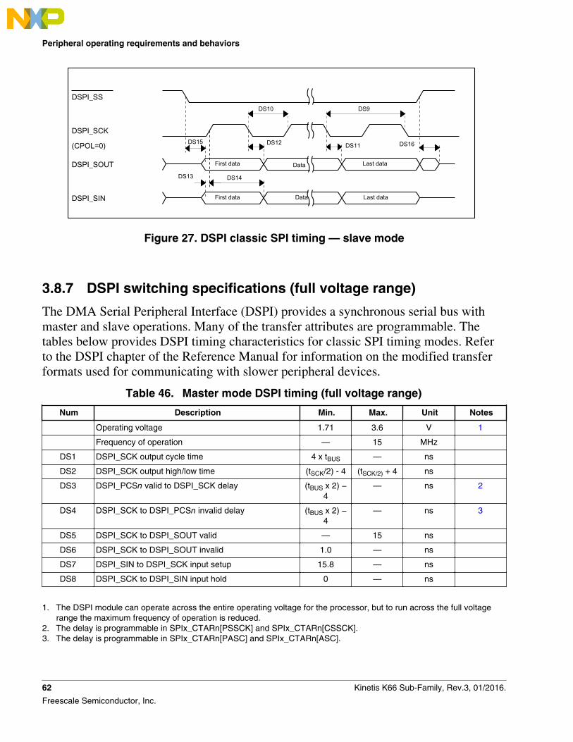
First data Last data
First data Data Last data
Data
DS15
DS10 DS9
DS16DS11DS12
DS14DS13
DSPI_SS
DSPI_SCK
(CPOL=0)
DSPI_SOUT
DSPI_SIN
Figure 27. DSPI classic SPI timing — slave mode
3.8.7 DSPI switching specifications (full voltage range)
The DMA Serial Peripheral Interface (DSPI) provides a synchronous serial bus withmaster and slave operations. Many of the transfer attributes are programmable. Thetables below provides DSPI timing characteristics for classic SPI timing modes. Referto the DSPI chapter of the Reference Manual for information on the modified transferformats used for communicating with slower peripheral devices.
Table 46. Master mode DSPI timing (full voltage range)
Num Description Min. Max. Unit Notes
Operating voltage 1.71 3.6 V 1
Frequency of operation — 15 MHz
DS1 DSPI_SCK output cycle time 4 x tBUS — ns
DS2 DSPI_SCK output high/low time (tSCK/2) - 4 (tSCK/2) + 4 ns
DS3 DSPI_PCSn valid to DSPI_SCK delay (tBUS x 2) −4
— ns 2
DS4 DSPI_SCK to DSPI_PCSn invalid delay (tBUS x 2) −4
— ns 3
DS5 DSPI_SCK to DSPI_SOUT valid — 15 ns
DS6 DSPI_SCK to DSPI_SOUT invalid 1.0 — ns
DS7 DSPI_SIN to DSPI_SCK input setup 15.8 — ns
DS8 DSPI_SCK to DSPI_SIN input hold 0 — ns
1. The DSPI module can operate across the entire operating voltage for the processor, but to run across the full voltagerange the maximum frequency of operation is reduced.
2. The delay is programmable in SPIx_CTARn[PSSCK] and SPIx_CTARn[CSSCK].3. The delay is programmable in SPIx_CTARn[PASC] and SPIx_CTARn[ASC].
Peripheral operating requirements and behaviors
62 Kinetis K66 Sub-Family, Rev.3, 01/2016.
Freescale Semiconductor, Inc.
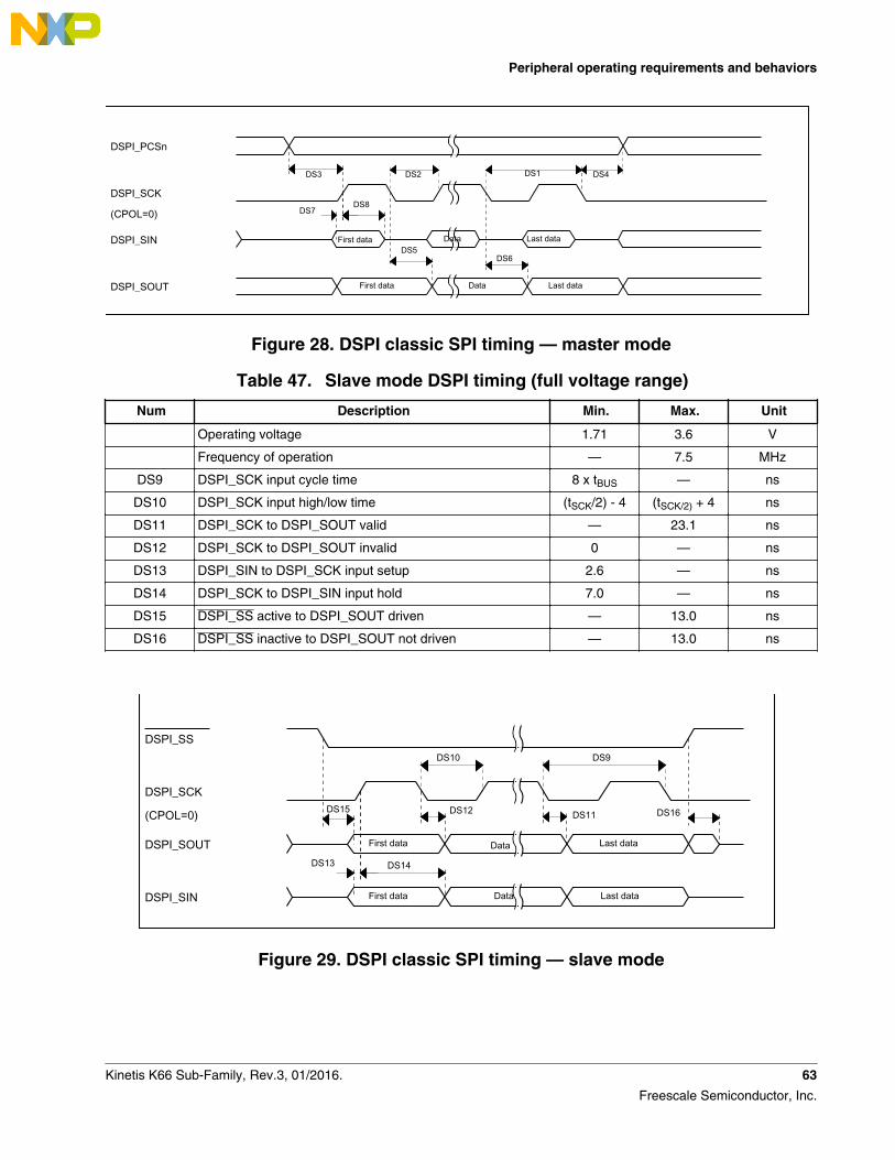
DS3 DS4DS1DS2
DS7DS8
First data Last dataDS5
First data Data Last data
DS6
Data
DSPI_PCSn
DSPI_SCK
(CPOL=0)
DSPI_SIN
DSPI_SOUT
Figure 28. DSPI classic SPI timing — master mode
Table 47. Slave mode DSPI timing (full voltage range)
Num Description Min. Max. Unit
Operating voltage 1.71 3.6 V
Frequency of operation — 7.5 MHz
DS9 DSPI_SCK input cycle time 8 x tBUS — ns
DS10 DSPI_SCK input high/low time (tSCK/2) - 4 (tSCK/2) + 4 ns
DS11 DSPI_SCK to DSPI_SOUT valid — 23.1 ns
DS12 DSPI_SCK to DSPI_SOUT invalid 0 — ns
DS13 DSPI_SIN to DSPI_SCK input setup 2.6 — ns
DS14 DSPI_SCK to DSPI_SIN input hold 7.0 — ns
DS15 DSPI_SS active to DSPI_SOUT driven — 13.0 ns
DS16 DSPI_SS inactive to DSPI_SOUT not driven — 13.0 ns
First data Last data
First data Data Last data
Data
DS15
DS10 DS9
DS16DS11DS12
DS14DS13
DSPI_SS
DSPI_SCK
(CPOL=0)
DSPI_SOUT
DSPI_SIN
Figure 29. DSPI classic SPI timing — slave mode
Peripheral operating requirements and behaviors
Kinetis K66 Sub-Family, Rev.3, 01/2016. 63
Freescale Semiconductor, Inc.
3.8.8 I2C switching specifications
See General switching specifications.
3.8.9 UART switching specifications
See General switching specifications.
3.8.10 Low Power UART switching specifications
See General switching specifications.
3.8.11 SDHC specifications
The following timing specs are defined at the chip I/O pin and must be translatedappropriately to arrive at timing specs/constraints for the physical interface.
Table 48. SDHC full voltage range switching specifications
Num Symbol Description Min. Max. Unit
Operating voltage 1.71 3.6 V
Card input clock
SD1 fpp Clock frequency (low speed) 0 400 kHz
fpp Clock frequency (SD\SDIO full speed\high speed) 0 25\50 MHz
fpp Clock frequency (MMC full speed\high speed) 0 20\50 MHz
fOD Clock frequency (identification mode) 0 400 kHz
SD2 tWL Clock low time 7 — ns
SD3 tWH Clock high time 7 — ns
SD4 tTLH Clock rise time — 3 ns
SD5 tTHL Clock fall time — 3 ns
SDHC output / card inputs SDHC_CMD, SDHC_DAT (reference to SDHC_CLK)
SD6 tOD SDHC output delay (output valid) -5 8.6 8.3 ns
SDHC input / card inputs SDHC_CMD, SDHC_DAT (reference to SDHC_CLK)
SD7 tISU SDHC input setup time 5 — ns
SD8 tIH SDHC input hold time 0 — ns
Peripheral operating requirements and behaviors
64 Kinetis K66 Sub-Family, Rev.3, 01/2016.
Freescale Semiconductor, Inc.
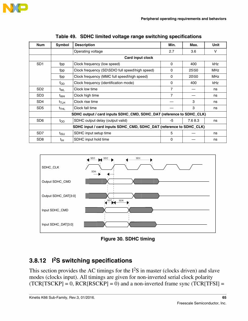
Table 49. SDHC limited voltage range switching specifications
Num Symbol Description Min. Max. Unit
Operating voltage 2.7 3.6 V
Card input clock
SD1 fpp Clock frequency (low speed) 0 400 kHz
fpp Clock frequency (SD\SDIO full speed\high speed) 0 25\50 MHz
fpp Clock frequency (MMC full speed\high speed) 0 20\50 MHz
fOD Clock frequency (identification mode) 0 400 kHz
SD2 tWL Clock low time 7 — ns
SD3 tWH Clock high time 7 — ns
SD4 tTLH Clock rise time — 3 ns
SD5 tTHL Clock fall time — 3 ns
SDHC output / card inputs SDHC_CMD, SDHC_DAT (reference to SDHC_CLK)
SD6 tOD SDHC output delay (output valid) -5 7.6 8.3 ns
SDHC input / card inputs SDHC_CMD, SDHC_DAT (reference to SDHC_CLK)
SD7 tISU SDHC input setup time 5 — ns
SD8 tIH SDHC input hold time 0 — ns
SD2SD3 SD1
SD6
SD8SD7
SDHC_CLK
Output SDHC_CMD
Output SDHC_DAT[3:0]
Input SDHC_CMD
Input SDHC_DAT[3:0]
Figure 30. SDHC timing
3.8.12 I2S switching specifications
This section provides the AC timings for the I2S in master (clocks driven) and slavemodes (clocks input). All timings are given for non-inverted serial clock polarity(TCR[TSCKP] = 0, RCR[RSCKP] = 0) and a non-inverted frame sync (TCR[TFSI] =
Peripheral operating requirements and behaviors
Kinetis K66 Sub-Family, Rev.3, 01/2016. 65
Freescale Semiconductor, Inc.
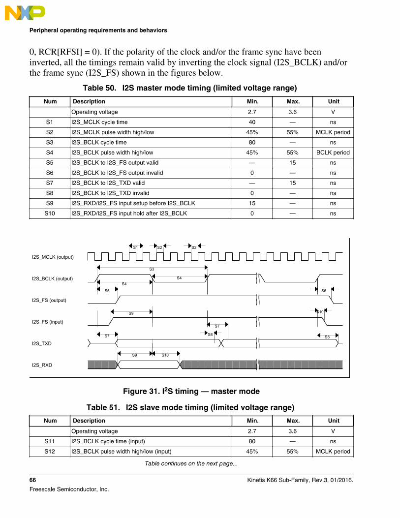
0, RCR[RFSI] = 0). If the polarity of the clock and/or the frame sync have beeninverted, all the timings remain valid by inverting the clock signal (I2S_BCLK) and/orthe frame sync (I2S_FS) shown in the figures below.
Table 50. I2S master mode timing (limited voltage range)
Num Description Min. Max. Unit
Operating voltage 2.7 3.6 V
S1 I2S_MCLK cycle time 40 — ns
S2 I2S_MCLK pulse width high/low 45% 55% MCLK period
S3 I2S_BCLK cycle time 80 — ns
S4 I2S_BCLK pulse width high/low 45% 55% BCLK period
S5 I2S_BCLK to I2S_FS output valid — 15 ns
S6 I2S_BCLK to I2S_FS output invalid 0 — ns
S7 I2S_BCLK to I2S_TXD valid — 15 ns
S8 I2S_BCLK to I2S_TXD invalid 0 — ns
S9 I2S_RXD/I2S_FS input setup before I2S_BCLK 15 — ns
S10 I2S_RXD/I2S_FS input hold after I2S_BCLK 0 — ns
S1 S2 S2
S3
S4S4
S5
S9
S7
S9 S10
S7
S8
S6
S10
S8
I2S_MCLK (output)
I2S_BCLK (output)
I2S_FS (output)
I2S_FS (input)
I2S_TXD
I2S_RXD
Figure 31. I2S timing — master mode
Table 51. I2S slave mode timing (limited voltage range)
Num Description Min. Max. Unit
Operating voltage 2.7 3.6 V
S11 I2S_BCLK cycle time (input) 80 — ns
S12 I2S_BCLK pulse width high/low (input) 45% 55% MCLK period
Table continues on the next page...
Peripheral operating requirements and behaviors
66 Kinetis K66 Sub-Family, Rev.3, 01/2016.
Freescale Semiconductor, Inc.
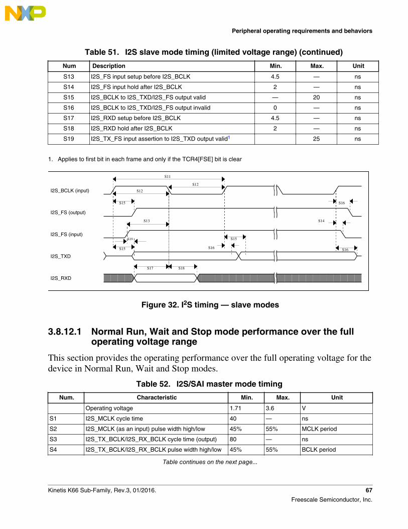
Table 51. I2S slave mode timing (limited voltage range) (continued)
Num Description Min. Max. Unit
S13 I2S_FS input setup before I2S_BCLK 4.5 — ns
S14 I2S_FS input hold after I2S_BCLK 2 — ns
S15 I2S_BCLK to I2S_TXD/I2S_FS output valid — 20 ns
S16 I2S_BCLK to I2S_TXD/I2S_FS output invalid 0 — ns
S17 I2S_RXD setup before I2S_BCLK 4.5 — ns
S18 I2S_RXD hold after I2S_BCLK 2 — ns
S19 I2S_TX_FS input assertion to I2S_TXD output valid1 25 ns
1. Applies to first bit in each frame and only if the TCR4[FSE] bit is clear
S15
S13
S15
S17 S18
S15
S16
S16
S14
S16
S11
S12
S12
I2S_BCLK (input)
I2S_FS (output)
I2S_FS (input)
I2S_TXD
I2S_RXD
S19
Figure 32. I2S timing — slave modes
3.8.12.1 Normal Run, Wait and Stop mode performance over the fulloperating voltage range
This section provides the operating performance over the full operating voltage for thedevice in Normal Run, Wait and Stop modes.
Table 52. I2S/SAI master mode timing
Num. Characteristic Min. Max. Unit
Operating voltage 1.71 3.6 V
S1 I2S_MCLK cycle time 40 — ns
S2 I2S_MCLK (as an input) pulse width high/low 45% 55% MCLK period
S3 I2S_TX_BCLK/I2S_RX_BCLK cycle time (output) 80 — ns
S4 I2S_TX_BCLK/I2S_RX_BCLK pulse width high/low 45% 55% BCLK period
Table continues on the next page...
Peripheral operating requirements and behaviors
Kinetis K66 Sub-Family, Rev.3, 01/2016. 67
Freescale Semiconductor, Inc.
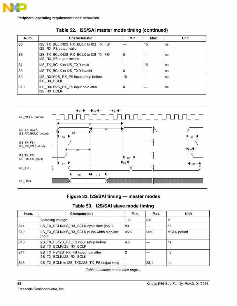
Table 52. I2S/SAI master mode timing (continued)
Num. Characteristic Min. Max. Unit
S5 I2S_TX_BCLK/I2S_RX_BCLK to I2S_TX_FS/I2S_RX_FS output valid
— 15 ns
S6 I2S_TX_BCLK/I2S_RX_BCLK to I2S_TX_FS/I2S_RX_FS output invalid
0 — ns
S7 I2S_TX_BCLK to I2S_TXD valid — 15 ns
S8 I2S_TX_BCLK to I2S_TXD invalid 0 — ns
S9 I2S_RXD/I2S_RX_FS input setup beforeI2S_RX_BCLK
15 — ns
S10 I2S_RXD/I2S_RX_FS input hold afterI2S_RX_BCLK
0 — ns
S1 S2 S2
S3
S4S4
S5
S9
S7
S9 S10
S7
S8
S6
S10
S8
I2S_MCLK (output)
I2S_TX_BCLK/ I2S_RX_BCLK (output)
I2S_TX_FS/ I2S_RX_FS (output)
I2S_TX_FS/ I2S_RX_FS (input)
I2S_TXD
I2S_RXD
Figure 33. I2S/SAI timing — master modes
Table 53. I2S/SAI slave mode timing
Num. Characteristic Min. Max. Unit
Operating voltage 1.71 3.6 V
S11 I2S_TX_BCLK/I2S_RX_BCLK cycle time (input) 80 — ns
S12 I2S_TX_BCLK/I2S_RX_BCLK pulse width high/low(input)
45% 55% MCLK period
S13 I2S_TX_FS/I2S_RX_FS input setup beforeI2S_TX_BCLK/I2S_RX_BCLK
4.5 — ns
S14 I2S_TX_FS/I2S_RX_FS input hold afterI2S_TX_BCLK/I2S_RX_BCLK
2 — ns
S15 I2S_TX_BCLK to I2S_TXD/I2S_TX_FS output valid — 23.1 ns
Table continues on the next page...
Peripheral operating requirements and behaviors
68 Kinetis K66 Sub-Family, Rev.3, 01/2016.
Freescale Semiconductor, Inc.
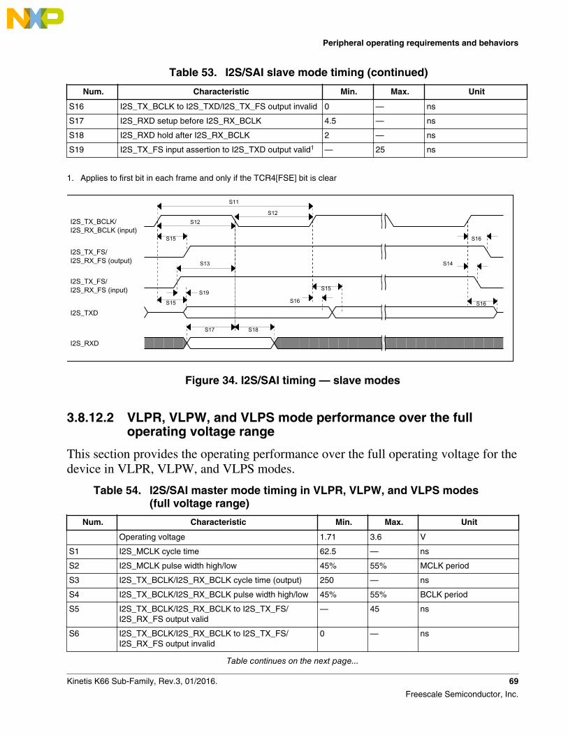
Table 53. I2S/SAI slave mode timing (continued)
Num. Characteristic Min. Max. Unit
S16 I2S_TX_BCLK to I2S_TXD/I2S_TX_FS output invalid 0 — ns
S17 I2S_RXD setup before I2S_RX_BCLK 4.5 — ns
S18 I2S_RXD hold after I2S_RX_BCLK 2 — ns
S19 I2S_TX_FS input assertion to I2S_TXD output valid1 — 25 ns
1. Applies to first bit in each frame and only if the TCR4[FSE] bit is clear
S15
S13
S15
S17 S18
S15
S16
S16
S14
S16
S11
S12S12
I2S_TX_BCLK/ I2S_RX_BCLK (input)
I2S_TX_FS/ I2S_RX_FS (output)
I2S_TXD
I2S_RXD
I2S_TX_FS/ I2S_RX_FS (input) S19
Figure 34. I2S/SAI timing — slave modes
3.8.12.2 VLPR, VLPW, and VLPS mode performance over the fulloperating voltage range
This section provides the operating performance over the full operating voltage for thedevice in VLPR, VLPW, and VLPS modes.
Table 54. I2S/SAI master mode timing in VLPR, VLPW, and VLPS modes(full voltage range)
Num. Characteristic Min. Max. Unit
Operating voltage 1.71 3.6 V
S1 I2S_MCLK cycle time 62.5 — ns
S2 I2S_MCLK pulse width high/low 45% 55% MCLK period
S3 I2S_TX_BCLK/I2S_RX_BCLK cycle time (output) 250 — ns
S4 I2S_TX_BCLK/I2S_RX_BCLK pulse width high/low 45% 55% BCLK period
S5 I2S_TX_BCLK/I2S_RX_BCLK to I2S_TX_FS/I2S_RX_FS output valid
— 45 ns
S6 I2S_TX_BCLK/I2S_RX_BCLK to I2S_TX_FS/I2S_RX_FS output invalid
0 — ns
Table continues on the next page...
Peripheral operating requirements and behaviors
Kinetis K66 Sub-Family, Rev.3, 01/2016. 69
Freescale Semiconductor, Inc.
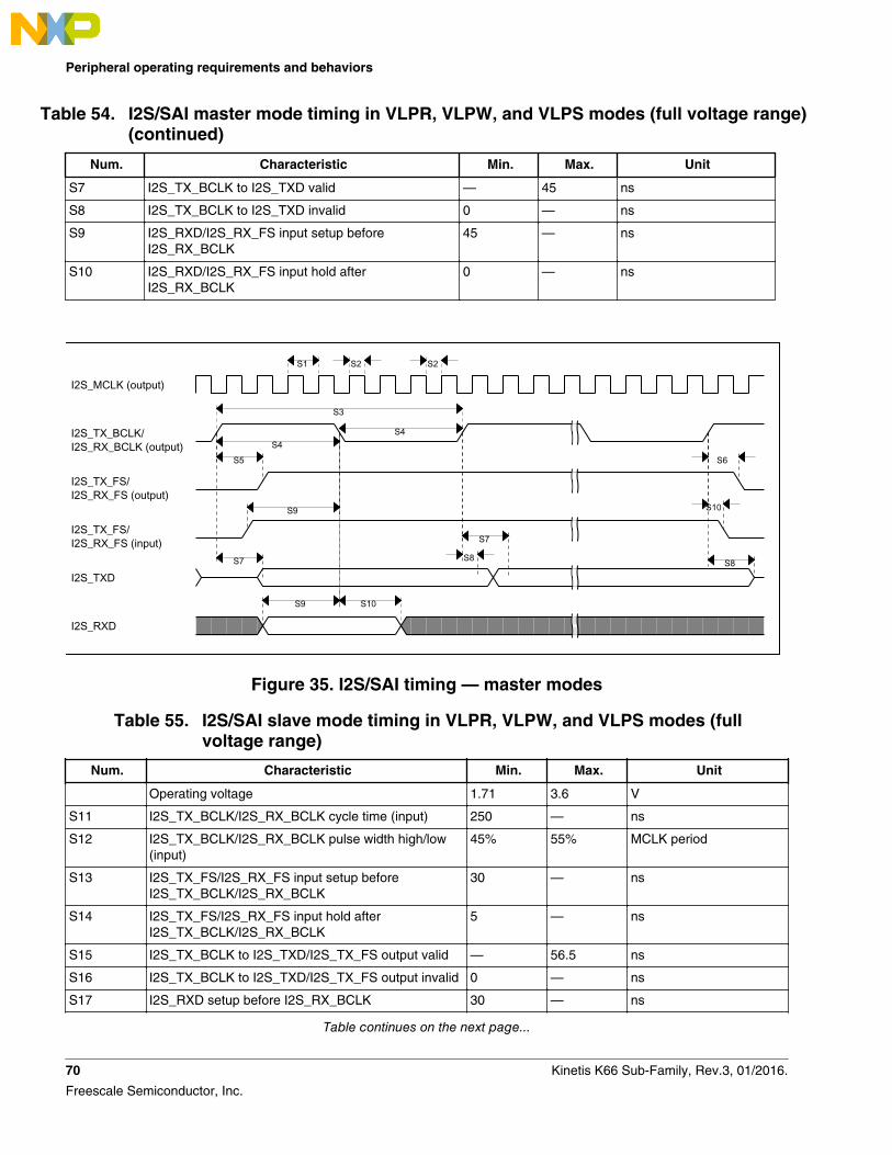
Table 54. I2S/SAI master mode timing in VLPR, VLPW, and VLPS modes (full voltage range)(continued)
Num. Characteristic Min. Max. Unit
S7 I2S_TX_BCLK to I2S_TXD valid — 45 ns
S8 I2S_TX_BCLK to I2S_TXD invalid 0 — ns
S9 I2S_RXD/I2S_RX_FS input setup beforeI2S_RX_BCLK
45 — ns
S10 I2S_RXD/I2S_RX_FS input hold afterI2S_RX_BCLK
0 — ns
S1 S2 S2
S3
S4S4
S5
S9
S7
S9 S10
S7
S8
S6
S10
S8
I2S_MCLK (output)
I2S_TX_BCLK/ I2S_RX_BCLK (output)
I2S_TX_FS/ I2S_RX_FS (output)
I2S_TX_FS/ I2S_RX_FS (input)
I2S_TXD
I2S_RXD
Figure 35. I2S/SAI timing — master modes
Table 55. I2S/SAI slave mode timing in VLPR, VLPW, and VLPS modes (fullvoltage range)
Num. Characteristic Min. Max. Unit
Operating voltage 1.71 3.6 V
S11 I2S_TX_BCLK/I2S_RX_BCLK cycle time (input) 250 — ns
S12 I2S_TX_BCLK/I2S_RX_BCLK pulse width high/low(input)
45% 55% MCLK period
S13 I2S_TX_FS/I2S_RX_FS input setup beforeI2S_TX_BCLK/I2S_RX_BCLK
30 — ns
S14 I2S_TX_FS/I2S_RX_FS input hold afterI2S_TX_BCLK/I2S_RX_BCLK
5 — ns
S15 I2S_TX_BCLK to I2S_TXD/I2S_TX_FS output valid — 56.5 ns
S16 I2S_TX_BCLK to I2S_TXD/I2S_TX_FS output invalid 0 — ns
S17 I2S_RXD setup before I2S_RX_BCLK 30 — ns
Table continues on the next page...
Peripheral operating requirements and behaviors
70 Kinetis K66 Sub-Family, Rev.3, 01/2016.
Freescale Semiconductor, Inc.
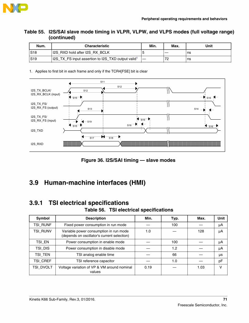
Table 55. I2S/SAI slave mode timing in VLPR, VLPW, and VLPS modes (full voltage range)(continued)
Num. Characteristic Min. Max. Unit
S18 I2S_RXD hold after I2S_RX_BCLK 5 — ns
S19 I2S_TX_FS input assertion to I2S_TXD output valid1 — 72 ns
1. Applies to first bit in each frame and only if the TCR4[FSE] bit is clear
S15
S13
S15
S17 S18
S15
S16
S16
S14
S16
S11
S12S12
I2S_TX_BCLK/ I2S_RX_BCLK (input)
I2S_TX_FS/ I2S_RX_FS (output)
I2S_TXD
I2S_RXD
I2S_TX_FS/ I2S_RX_FS (input) S19
Figure 36. I2S/SAI timing — slave modes
3.9 Human-machine interfaces (HMI)
3.9.1 TSI electrical specificationsTable 56. TSI electrical specifications
Symbol Description Min. Typ. Max. Unit
TSI_RUNF Fixed power consumption in run mode — 100 — µA
TSI_RUNV Variable power consumption in run mode(depends on oscillator's current selection)
1.0 — 128 µA
TSI_EN Power consumption in enable mode — 100 — µA
TSI_DIS Power consumption in disable mode — 1.2 — µA
TSI_TEN TSI analog enable time — 66 — µs
TSI_CREF TSI reference capacitor — 1.0 — pF
TSI_DVOLT Voltage variation of VP & VM around nominalvalues
0.19 — 1.03 V
Peripheral operating requirements and behaviors
Kinetis K66 Sub-Family, Rev.3, 01/2016. 71
Freescale Semiconductor, Inc.
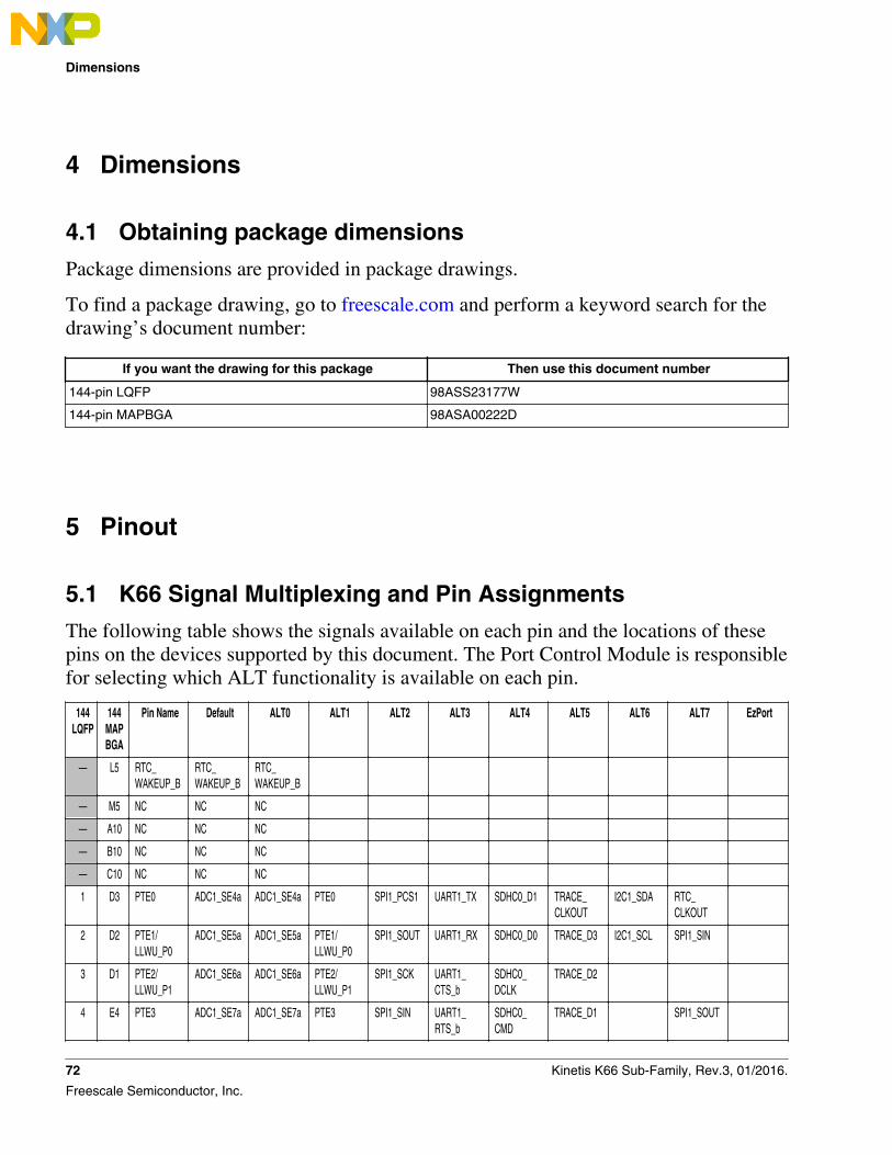
4 Dimensions
4.1 Obtaining package dimensions
Package dimensions are provided in package drawings.
To find a package drawing, go to freescale.com and perform a keyword search for thedrawing’s document number:
If you want the drawing for this package Then use this document number
144-pin LQFP 98ASS23177W
144-pin MAPBGA 98ASA00222D
5 Pinout
5.1 K66 Signal Multiplexing and Pin Assignments
The following table shows the signals available on each pin and the locations of thesepins on the devices supported by this document. The Port Control Module is responsiblefor selecting which ALT functionality is available on each pin.
144LQFP
144MAPBGA
Pin Name Default ALT0 ALT1 ALT2 ALT3 ALT4 ALT5 ALT6 ALT7 EzPort
— L5 RTC_WAKEUP_B
RTC_WAKEUP_B
RTC_WAKEUP_B
— M5 NC NC NC
— A10 NC NC NC
— B10 NC NC NC
— C10 NC NC NC
1 D3 PTE0 ADC1_SE4a ADC1_SE4a PTE0 SPI1_PCS1 UART1_TX SDHC0_D1 TRACE_CLKOUT
I2C1_SDA RTC_CLKOUT
2 D2 PTE1/LLWU_P0
ADC1_SE5a ADC1_SE5a PTE1/LLWU_P0
SPI1_SOUT UART1_RX SDHC0_D0 TRACE_D3 I2C1_SCL SPI1_SIN
3 D1 PTE2/LLWU_P1
ADC1_SE6a ADC1_SE6a PTE2/LLWU_P1
SPI1_SCK UART1_CTS_b
SDHC0_DCLK
TRACE_D2
4 E4 PTE3 ADC1_SE7a ADC1_SE7a PTE3 SPI1_SIN UART1_RTS_b
SDHC0_CMD
TRACE_D1 SPI1_SOUT
Dimensions
72 Kinetis K66 Sub-Family, Rev.3, 01/2016.
Freescale Semiconductor, Inc.
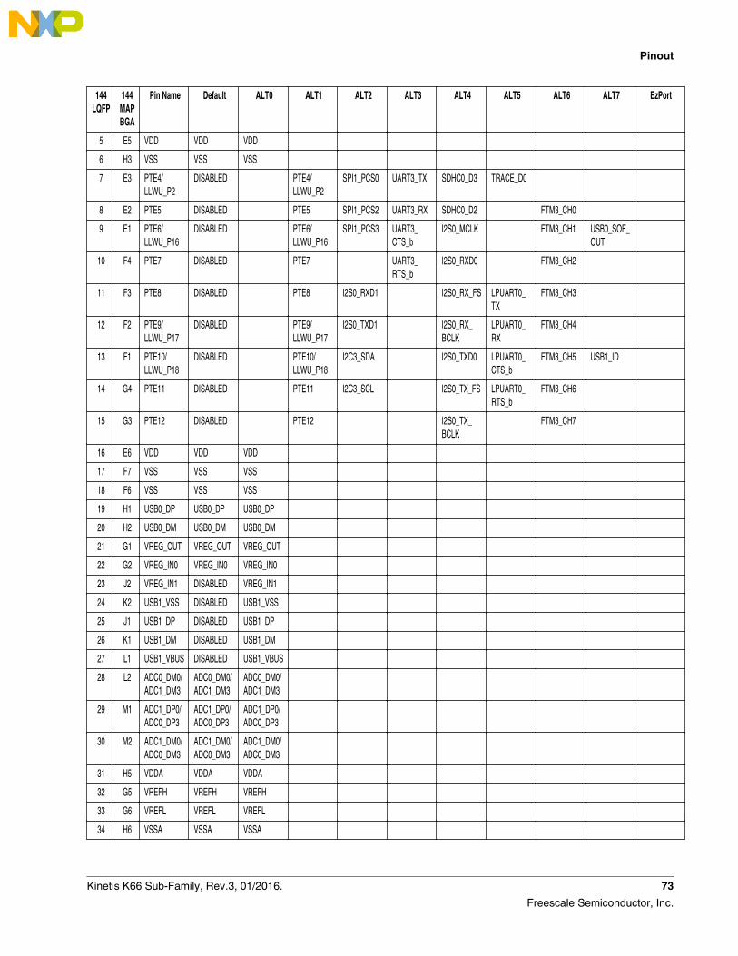
144LQFP
144MAPBGA
Pin Name Default ALT0 ALT1 ALT2 ALT3 ALT4 ALT5 ALT6 ALT7 EzPort
5 E5 VDD VDD VDD
6 H3 VSS VSS VSS
7 E3 PTE4/LLWU_P2
DISABLED PTE4/LLWU_P2
SPI1_PCS0 UART3_TX SDHC0_D3 TRACE_D0
8 E2 PTE5 DISABLED PTE5 SPI1_PCS2 UART3_RX SDHC0_D2 FTM3_CH0
9 E1 PTE6/LLWU_P16
DISABLED PTE6/LLWU_P16
SPI1_PCS3 UART3_CTS_b
I2S0_MCLK FTM3_CH1 USB0_SOF_OUT
10 F4 PTE7 DISABLED PTE7 UART3_RTS_b
I2S0_RXD0 FTM3_CH2
11 F3 PTE8 DISABLED PTE8 I2S0_RXD1 I2S0_RX_FS LPUART0_TX
FTM3_CH3
12 F2 PTE9/LLWU_P17
DISABLED PTE9/LLWU_P17
I2S0_TXD1 I2S0_RX_BCLK
LPUART0_RX
FTM3_CH4
13 F1 PTE10/LLWU_P18
DISABLED PTE10/LLWU_P18
I2C3_SDA I2S0_TXD0 LPUART0_CTS_b
FTM3_CH5 USB1_ID
14 G4 PTE11 DISABLED PTE11 I2C3_SCL I2S0_TX_FS LPUART0_RTS_b
FTM3_CH6
15 G3 PTE12 DISABLED PTE12 I2S0_TX_BCLK
FTM3_CH7
16 E6 VDD VDD VDD
17 F7 VSS VSS VSS
18 F6 VSS VSS VSS
19 H1 USB0_DP USB0_DP USB0_DP
20 H2 USB0_DM USB0_DM USB0_DM
21 G1 VREG_OUT VREG_OUT VREG_OUT
22 G2 VREG_IN0 VREG_IN0 VREG_IN0
23 J2 VREG_IN1 DISABLED VREG_IN1
24 K2 USB1_VSS DISABLED USB1_VSS
25 J1 USB1_DP DISABLED USB1_DP
26 K1 USB1_DM DISABLED USB1_DM
27 L1 USB1_VBUS DISABLED USB1_VBUS
28 L2 ADC0_DM0/ADC1_DM3
ADC0_DM0/ADC1_DM3
ADC0_DM0/ADC1_DM3
29 M1 ADC1_DP0/ADC0_DP3
ADC1_DP0/ADC0_DP3
ADC1_DP0/ADC0_DP3
30 M2 ADC1_DM0/ADC0_DM3
ADC1_DM0/ADC0_DM3
ADC1_DM0/ADC0_DM3
31 H5 VDDA VDDA VDDA
32 G5 VREFH VREFH VREFH
33 G6 VREFL VREFL VREFL
34 H6 VSSA VSSA VSSA
Pinout
Kinetis K66 Sub-Family, Rev.3, 01/2016. 73
Freescale Semiconductor, Inc.
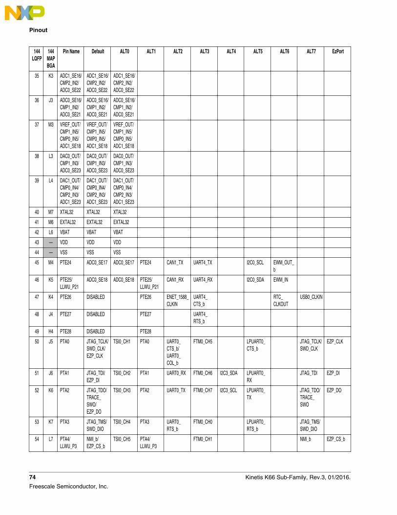
144LQFP
144MAPBGA
Pin Name Default ALT0 ALT1 ALT2 ALT3 ALT4 ALT5 ALT6 ALT7 EzPort
35 K3 ADC1_SE16/CMP2_IN2/ADC0_SE22
ADC1_SE16/CMP2_IN2/ADC0_SE22
ADC1_SE16/CMP2_IN2/ADC0_SE22
36 J3 ADC0_SE16/CMP1_IN2/ADC0_SE21
ADC0_SE16/CMP1_IN2/ADC0_SE21
ADC0_SE16/CMP1_IN2/ADC0_SE21
37 M3 VREF_OUT/CMP1_IN5/CMP0_IN5/ADC1_SE18
VREF_OUT/CMP1_IN5/CMP0_IN5/ADC1_SE18
VREF_OUT/CMP1_IN5/CMP0_IN5/ADC1_SE18
38 L3 DAC0_OUT/CMP1_IN3/ADC0_SE23
DAC0_OUT/CMP1_IN3/ADC0_SE23
DAC0_OUT/CMP1_IN3/ADC0_SE23
39 L4 DAC1_OUT/CMP0_IN4/CMP2_IN3/ADC1_SE23
DAC1_OUT/CMP0_IN4/CMP2_IN3/ADC1_SE23
DAC1_OUT/CMP0_IN4/CMP2_IN3/ADC1_SE23
40 M7 XTAL32 XTAL32 XTAL32
41 M6 EXTAL32 EXTAL32 EXTAL32
42 L6 VBAT VBAT VBAT
43 — VDD VDD VDD
44 — VSS VSS VSS
45 M4 PTE24 ADC0_SE17 ADC0_SE17 PTE24 CAN1_TX UART4_TX I2C0_SCL EWM_OUT_b
46 K5 PTE25/LLWU_P21
ADC0_SE18 ADC0_SE18 PTE25/LLWU_P21
CAN1_RX UART4_RX I2C0_SDA EWM_IN
47 K4 PTE26 DISABLED PTE26 ENET_1588_CLKIN
UART4_CTS_b
RTC_CLKOUT
USB0_CLKIN
48 J4 PTE27 DISABLED PTE27 UART4_RTS_b
49 H4 PTE28 DISABLED PTE28
50 J5 PTA0 JTAG_TCLK/SWD_CLK/EZP_CLK
TSI0_CH1 PTA0 UART0_CTS_b/UART0_COL_b
FTM0_CH5 LPUART0_CTS_b
JTAG_TCLK/SWD_CLK
EZP_CLK
51 J6 PTA1 JTAG_TDI/EZP_DI
TSI0_CH2 PTA1 UART0_RX FTM0_CH6 I2C3_SDA LPUART0_RX
JTAG_TDI EZP_DI
52 K6 PTA2 JTAG_TDO/TRACE_SWO/EZP_DO
TSI0_CH3 PTA2 UART0_TX FTM0_CH7 I2C3_SCL LPUART0_TX
JTAG_TDO/TRACE_SWO
EZP_DO
53 K7 PTA3 JTAG_TMS/SWD_DIO
TSI0_CH4 PTA3 UART0_RTS_b
FTM0_CH0 LPUART0_RTS_b
JTAG_TMS/SWD_DIO
54 L7 PTA4/LLWU_P3
NMI_b/EZP_CS_b
TSI0_CH5 PTA4/LLWU_P3
FTM0_CH1 NMI_b EZP_CS_b
Pinout
74 Kinetis K66 Sub-Family, Rev.3, 01/2016.
Freescale Semiconductor, Inc.
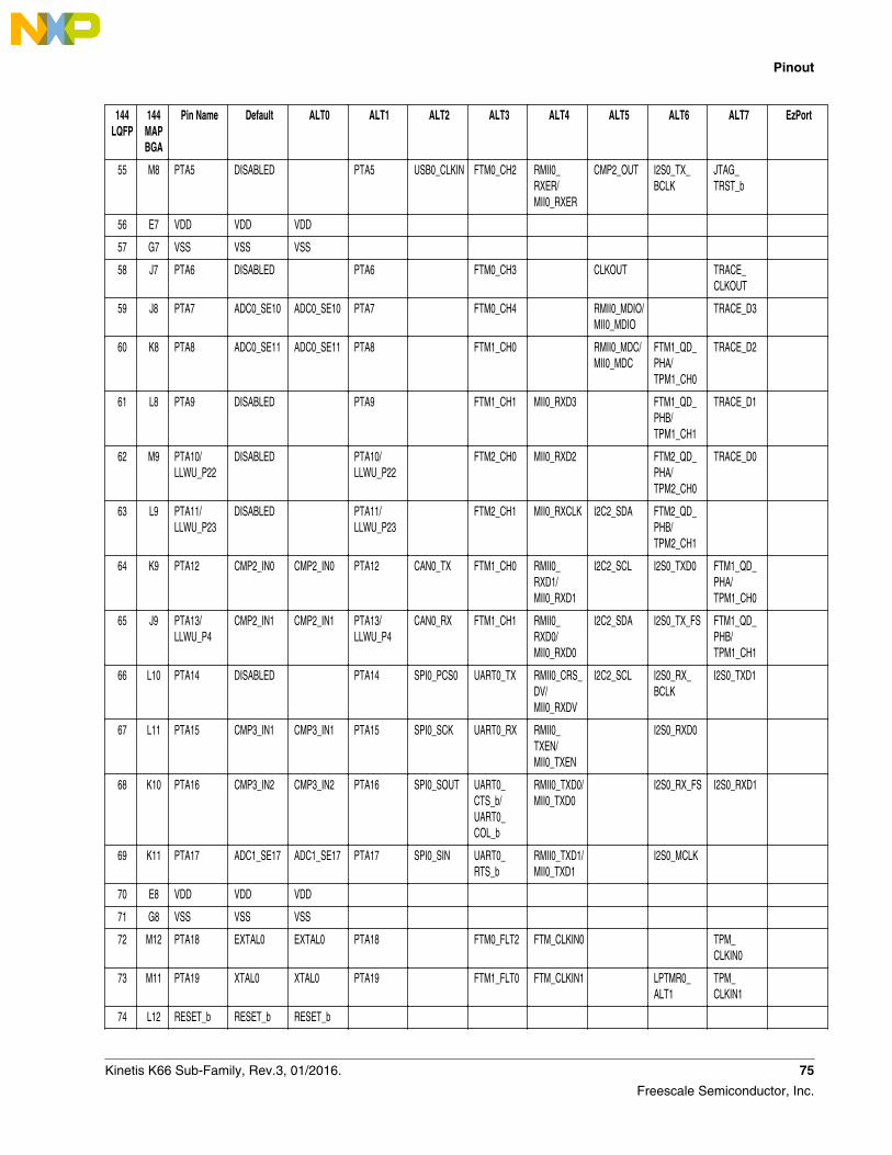
144LQFP
144MAPBGA
Pin Name Default ALT0 ALT1 ALT2 ALT3 ALT4 ALT5 ALT6 ALT7 EzPort
55 M8 PTA5 DISABLED PTA5 USB0_CLKIN FTM0_CH2 RMII0_RXER/MII0_RXER
CMP2_OUT I2S0_TX_BCLK
JTAG_TRST_b
56 E7 VDD VDD VDD
57 G7 VSS VSS VSS
58 J7 PTA6 DISABLED PTA6 FTM0_CH3 CLKOUT TRACE_CLKOUT
59 J8 PTA7 ADC0_SE10 ADC0_SE10 PTA7 FTM0_CH4 RMII0_MDIO/MII0_MDIO
TRACE_D3
60 K8 PTA8 ADC0_SE11 ADC0_SE11 PTA8 FTM1_CH0 RMII0_MDC/MII0_MDC
FTM1_QD_PHA/TPM1_CH0
TRACE_D2
61 L8 PTA9 DISABLED PTA9 FTM1_CH1 MII0_RXD3 FTM1_QD_PHB/TPM1_CH1
TRACE_D1
62 M9 PTA10/LLWU_P22
DISABLED PTA10/LLWU_P22
FTM2_CH0 MII0_RXD2 FTM2_QD_PHA/TPM2_CH0
TRACE_D0
63 L9 PTA11/LLWU_P23
DISABLED PTA11/LLWU_P23
FTM2_CH1 MII0_RXCLK I2C2_SDA FTM2_QD_PHB/TPM2_CH1
64 K9 PTA12 CMP2_IN0 CMP2_IN0 PTA12 CAN0_TX FTM1_CH0 RMII0_RXD1/MII0_RXD1
I2C2_SCL I2S0_TXD0 FTM1_QD_PHA/TPM1_CH0
65 J9 PTA13/LLWU_P4
CMP2_IN1 CMP2_IN1 PTA13/LLWU_P4
CAN0_RX FTM1_CH1 RMII0_RXD0/MII0_RXD0
I2C2_SDA I2S0_TX_FS FTM1_QD_PHB/TPM1_CH1
66 L10 PTA14 DISABLED PTA14 SPI0_PCS0 UART0_TX RMII0_CRS_DV/MII0_RXDV
I2C2_SCL I2S0_RX_BCLK
I2S0_TXD1
67 L11 PTA15 CMP3_IN1 CMP3_IN1 PTA15 SPI0_SCK UART0_RX RMII0_TXEN/MII0_TXEN
I2S0_RXD0
68 K10 PTA16 CMP3_IN2 CMP3_IN2 PTA16 SPI0_SOUT UART0_CTS_b/UART0_COL_b
RMII0_TXD0/MII0_TXD0
I2S0_RX_FS I2S0_RXD1
69 K11 PTA17 ADC1_SE17 ADC1_SE17 PTA17 SPI0_SIN UART0_RTS_b
RMII0_TXD1/MII0_TXD1
I2S0_MCLK
70 E8 VDD VDD VDD
71 G8 VSS VSS VSS
72 M12 PTA18 EXTAL0 EXTAL0 PTA18 FTM0_FLT2 FTM_CLKIN0 TPM_CLKIN0
73 M11 PTA19 XTAL0 XTAL0 PTA19 FTM1_FLT0 FTM_CLKIN1 LPTMR0_ALT1
TPM_CLKIN1
74 L12 RESET_b RESET_b RESET_b
Pinout
Kinetis K66 Sub-Family, Rev.3, 01/2016. 75
Freescale Semiconductor, Inc.
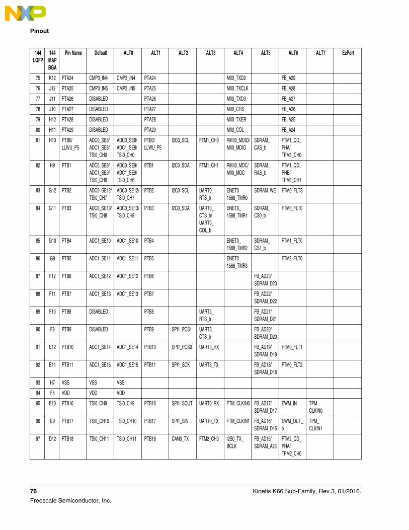
144LQFP
144MAPBGA
Pin Name Default ALT0 ALT1 ALT2 ALT3 ALT4 ALT5 ALT6 ALT7 EzPort
75 K12 PTA24 CMP3_IN4 CMP3_IN4 PTA24 MII0_TXD2 FB_A29
76 J12 PTA25 CMP3_IN5 CMP3_IN5 PTA25 MII0_TXCLK FB_A28
77 J11 PTA26 DISABLED PTA26 MII0_TXD3 FB_A27
78 J10 PTA27 DISABLED PTA27 MII0_CRS FB_A26
79 H12 PTA28 DISABLED PTA28 MII0_TXER FB_A25
80 H11 PTA29 DISABLED PTA29 MII0_COL FB_A24
81 H10 PTB0/LLWU_P5
ADC0_SE8/ADC1_SE8/TSI0_CH0
ADC0_SE8/ADC1_SE8/TSI0_CH0
PTB0/LLWU_P5
I2C0_SCL FTM1_CH0 RMII0_MDIO/MII0_MDIO
SDRAM_CAS_b
FTM1_QD_PHA/TPM1_CH0
82 H9 PTB1 ADC0_SE9/ADC1_SE9/TSI0_CH6
ADC0_SE9/ADC1_SE9/TSI0_CH6
PTB1 I2C0_SDA FTM1_CH1 RMII0_MDC/MII0_MDC
SDRAM_RAS_b
FTM1_QD_PHB/TPM1_CH1
83 G12 PTB2 ADC0_SE12/TSI0_CH7
ADC0_SE12/TSI0_CH7
PTB2 I2C0_SCL UART0_RTS_b
ENET0_1588_TMR0
SDRAM_WE FTM0_FLT3
84 G11 PTB3 ADC0_SE13/TSI0_CH8
ADC0_SE13/TSI0_CH8
PTB3 I2C0_SDA UART0_CTS_b/UART0_COL_b
ENET0_1588_TMR1
SDRAM_CS0_b
FTM0_FLT0
85 G10 PTB4 ADC1_SE10 ADC1_SE10 PTB4 ENET0_1588_TMR2
SDRAM_CS1_b
FTM1_FLT0
86 G9 PTB5 ADC1_SE11 ADC1_SE11 PTB5 ENET0_1588_TMR3
FTM2_FLT0
87 F12 PTB6 ADC1_SE12 ADC1_SE12 PTB6 FB_AD23/SDRAM_D23
88 F11 PTB7 ADC1_SE13 ADC1_SE13 PTB7 FB_AD22/SDRAM_D22
89 F10 PTB8 DISABLED PTB8 UART3_RTS_b
FB_AD21/SDRAM_D21
90 F9 PTB9 DISABLED PTB9 SPI1_PCS1 UART3_CTS_b
FB_AD20/SDRAM_D20
91 E12 PTB10 ADC1_SE14 ADC1_SE14 PTB10 SPI1_PCS0 UART3_RX FB_AD19/SDRAM_D19
FTM0_FLT1
92 E11 PTB11 ADC1_SE15 ADC1_SE15 PTB11 SPI1_SCK UART3_TX FB_AD18/SDRAM_D18
FTM0_FLT2
93 H7 VSS VSS VSS
94 F5 VDD VDD VDD
95 E10 PTB16 TSI0_CH9 TSI0_CH9 PTB16 SPI1_SOUT UART0_RX FTM_CLKIN0 FB_AD17/SDRAM_D17
EWM_IN TPM_CLKIN0
96 E9 PTB17 TSI0_CH10 TSI0_CH10 PTB17 SPI1_SIN UART0_TX FTM_CLKIN1 FB_AD16/SDRAM_D16
EWM_OUT_b
TPM_CLKIN1
97 D12 PTB18 TSI0_CH11 TSI0_CH11 PTB18 CAN0_TX FTM2_CH0 I2S0_TX_BCLK
FB_AD15/SDRAM_A23
FTM2_QD_PHA/TPM2_CH0
Pinout
76 Kinetis K66 Sub-Family, Rev.3, 01/2016.
Freescale Semiconductor, Inc.
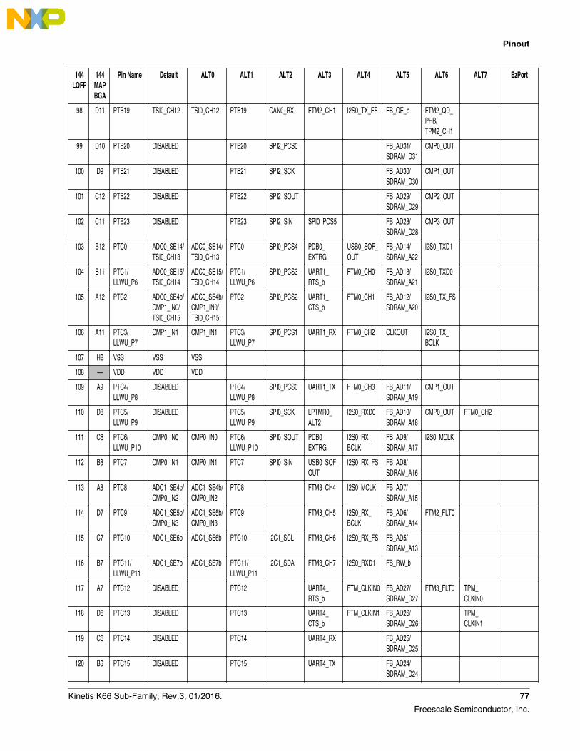
144LQFP
144MAPBGA
Pin Name Default ALT0 ALT1 ALT2 ALT3 ALT4 ALT5 ALT6 ALT7 EzPort
98 D11 PTB19 TSI0_CH12 TSI0_CH12 PTB19 CAN0_RX FTM2_CH1 I2S0_TX_FS FB_OE_b FTM2_QD_PHB/TPM2_CH1
99 D10 PTB20 DISABLED PTB20 SPI2_PCS0 FB_AD31/SDRAM_D31
CMP0_OUT
100 D9 PTB21 DISABLED PTB21 SPI2_SCK FB_AD30/SDRAM_D30
CMP1_OUT
101 C12 PTB22 DISABLED PTB22 SPI2_SOUT FB_AD29/SDRAM_D29
CMP2_OUT
102 C11 PTB23 DISABLED PTB23 SPI2_SIN SPI0_PCS5 FB_AD28/SDRAM_D28
CMP3_OUT
103 B12 PTC0 ADC0_SE14/TSI0_CH13
ADC0_SE14/TSI0_CH13
PTC0 SPI0_PCS4 PDB0_EXTRG
USB0_SOF_OUT
FB_AD14/SDRAM_A22
I2S0_TXD1
104 B11 PTC1/LLWU_P6
ADC0_SE15/TSI0_CH14
ADC0_SE15/TSI0_CH14
PTC1/LLWU_P6
SPI0_PCS3 UART1_RTS_b
FTM0_CH0 FB_AD13/SDRAM_A21
I2S0_TXD0
105 A12 PTC2 ADC0_SE4b/CMP1_IN0/TSI0_CH15
ADC0_SE4b/CMP1_IN0/TSI0_CH15
PTC2 SPI0_PCS2 UART1_CTS_b
FTM0_CH1 FB_AD12/SDRAM_A20
I2S0_TX_FS
106 A11 PTC3/LLWU_P7
CMP1_IN1 CMP1_IN1 PTC3/LLWU_P7
SPI0_PCS1 UART1_RX FTM0_CH2 CLKOUT I2S0_TX_BCLK
107 H8 VSS VSS VSS
108 — VDD VDD VDD
109 A9 PTC4/LLWU_P8
DISABLED PTC4/LLWU_P8
SPI0_PCS0 UART1_TX FTM0_CH3 FB_AD11/SDRAM_A19
CMP1_OUT
110 D8 PTC5/LLWU_P9
DISABLED PTC5/LLWU_P9
SPI0_SCK LPTMR0_ALT2
I2S0_RXD0 FB_AD10/SDRAM_A18
CMP0_OUT FTM0_CH2
111 C8 PTC6/LLWU_P10
CMP0_IN0 CMP0_IN0 PTC6/LLWU_P10
SPI0_SOUT PDB0_EXTRG
I2S0_RX_BCLK
FB_AD9/SDRAM_A17
I2S0_MCLK
112 B8 PTC7 CMP0_IN1 CMP0_IN1 PTC7 SPI0_SIN USB0_SOF_OUT
I2S0_RX_FS FB_AD8/SDRAM_A16
113 A8 PTC8 ADC1_SE4b/CMP0_IN2
ADC1_SE4b/CMP0_IN2
PTC8 FTM3_CH4 I2S0_MCLK FB_AD7/SDRAM_A15
114 D7 PTC9 ADC1_SE5b/CMP0_IN3
ADC1_SE5b/CMP0_IN3
PTC9 FTM3_CH5 I2S0_RX_BCLK
FB_AD6/SDRAM_A14
FTM2_FLT0
115 C7 PTC10 ADC1_SE6b ADC1_SE6b PTC10 I2C1_SCL FTM3_CH6 I2S0_RX_FS FB_AD5/SDRAM_A13
116 B7 PTC11/LLWU_P11
ADC1_SE7b ADC1_SE7b PTC11/LLWU_P11
I2C1_SDA FTM3_CH7 I2S0_RXD1 FB_RW_b
117 A7 PTC12 DISABLED PTC12 UART4_RTS_b
FTM_CLKIN0 FB_AD27/SDRAM_D27
FTM3_FLT0 TPM_CLKIN0
118 D6 PTC13 DISABLED PTC13 UART4_CTS_b
FTM_CLKIN1 FB_AD26/SDRAM_D26
TPM_CLKIN1
119 C6 PTC14 DISABLED PTC14 UART4_RX FB_AD25/SDRAM_D25
120 B6 PTC15 DISABLED PTC15 UART4_TX FB_AD24/SDRAM_D24
Pinout
Kinetis K66 Sub-Family, Rev.3, 01/2016. 77
Freescale Semiconductor, Inc.
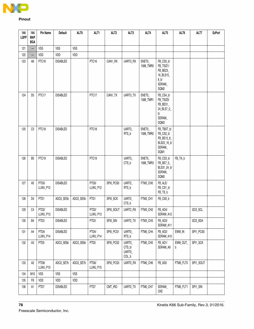
144LQFP
144MAPBGA
Pin Name Default ALT0 ALT1 ALT2 ALT3 ALT4 ALT5 ALT6 ALT7 EzPort
121 — VSS VSS VSS
122 — VDD VDD VDD
123 A6 PTC16 DISABLED PTC16 CAN1_RX UART3_RX ENET0_1588_TMR0
FB_CS5_b/FB_TSIZ1/FB_BE23_16_BLS15_8_b/SDRAM_DQM2
124 D5 PTC17 DISABLED PTC17 CAN1_TX UART3_TX ENET0_1588_TMR1
FB_CS4_b/FB_TSIZ0/FB_BE31_24_BLS7_0_b/SDRAM_DQM3
125 C5 PTC18 DISABLED PTC18 UART3_RTS_b
ENET0_1588_TMR2
FB_TBST_b/FB_CS2_b/FB_BE15_8_BLS23_16_b/SDRAM_DQM1
126 B5 PTC19 DISABLED PTC19 UART3_CTS_b
ENET0_1588_TMR3
FB_CS3_b/FB_BE7_0_BLS31_24_b/SDRAM_DQM0
FB_TA_b
127 A5 PTD0/LLWU_P12
DISABLED PTD0/LLWU_P12
SPI0_PCS0 UART2_RTS_b
FTM3_CH0 FB_ALE/FB_CS1_b/FB_TS_b
128 D4 PTD1 ADC0_SE5b ADC0_SE5b PTD1 SPI0_SCK UART2_CTS_b
FTM3_CH1 FB_CS0_b
129 C4 PTD2/LLWU_P13
DISABLED PTD2/LLWU_P13
SPI0_SOUT UART2_RX FTM3_CH2 FB_AD4/SDRAM_A12
I2C0_SCL
130 B4 PTD3 DISABLED PTD3 SPI0_SIN UART2_TX FTM3_CH3 FB_AD3/SDRAM_A11
I2C0_SDA
131 A4 PTD4/LLWU_P14
DISABLED PTD4/LLWU_P14
SPI0_PCS1 UART0_RTS_b
FTM0_CH4 FB_AD2/SDRAM_A10
EWM_IN SPI1_PCS0
132 A3 PTD5 ADC0_SE6b ADC0_SE6b PTD5 SPI0_PCS2 UART0_CTS_b/UART0_COL_b
FTM0_CH5 FB_AD1/SDRAM_A9
EWM_OUT_b
SPI1_SCK
133 A2 PTD6/LLWU_P15
ADC0_SE7b ADC0_SE7b PTD6/LLWU_P15
SPI0_PCS3 UART0_RX FTM0_CH6 FB_AD0 FTM0_FLT0 SPI1_SOUT
134 M10 VSS VSS VSS
135 F8 VDD VDD VDD
136 A1 PTD7 DISABLED PTD7 CMT_IRO UART0_TX FTM0_CH7 SDRAM_CKE
FTM0_FLT1 SPI1_SIN
Pinout
78 Kinetis K66 Sub-Family, Rev.3, 01/2016.
Freescale Semiconductor, Inc.
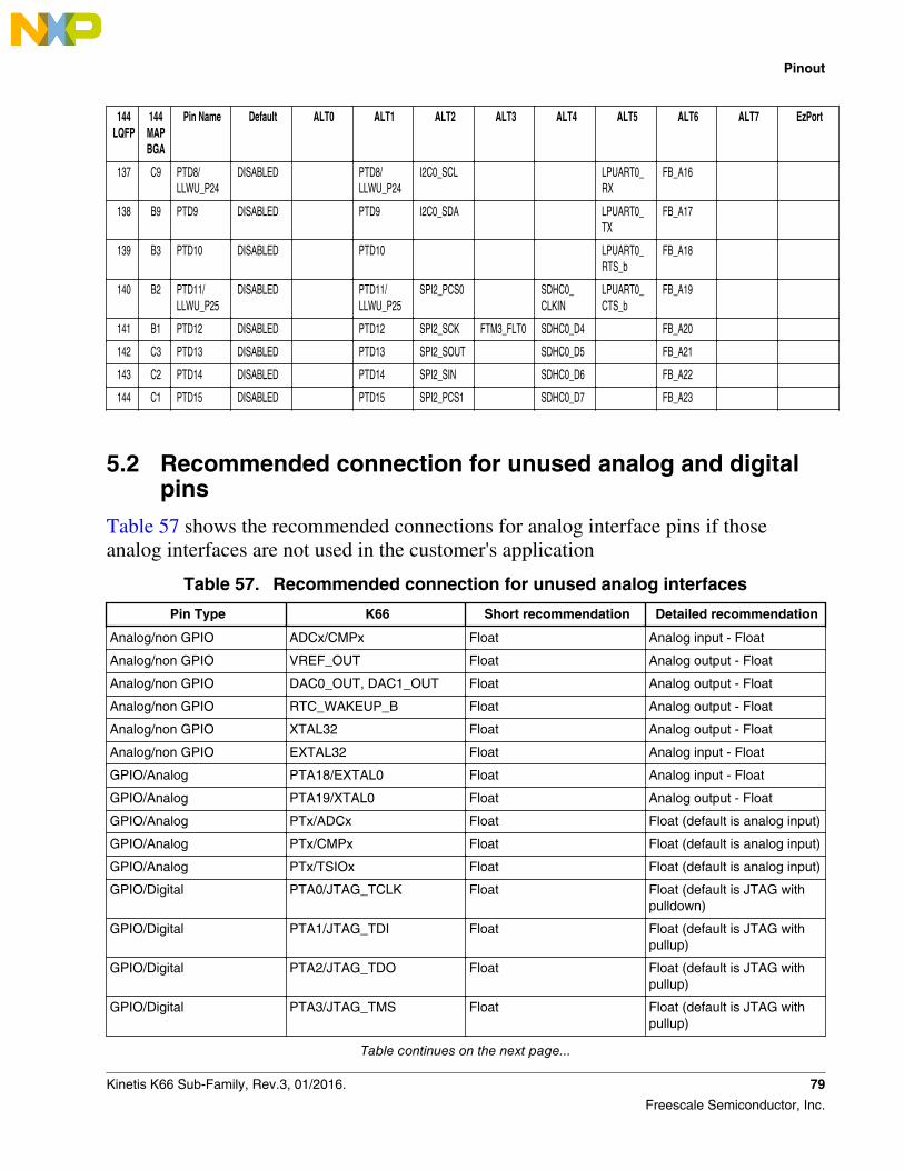
144LQFP
144MAPBGA
Pin Name Default ALT0 ALT1 ALT2 ALT3 ALT4 ALT5 ALT6 ALT7 EzPort
137 C9 PTD8/LLWU_P24
DISABLED PTD8/LLWU_P24
I2C0_SCL LPUART0_RX
FB_A16
138 B9 PTD9 DISABLED PTD9 I2C0_SDA LPUART0_TX
FB_A17
139 B3 PTD10 DISABLED PTD10 LPUART0_RTS_b
FB_A18
140 B2 PTD11/LLWU_P25
DISABLED PTD11/LLWU_P25
SPI2_PCS0 SDHC0_CLKIN
LPUART0_CTS_b
FB_A19
141 B1 PTD12 DISABLED PTD12 SPI2_SCK FTM3_FLT0 SDHC0_D4 FB_A20
142 C3 PTD13 DISABLED PTD13 SPI2_SOUT SDHC0_D5 FB_A21
143 C2 PTD14 DISABLED PTD14 SPI2_SIN SDHC0_D6 FB_A22
144 C1 PTD15 DISABLED PTD15 SPI2_PCS1 SDHC0_D7 FB_A23
5.2 Recommended connection for unused analog and digitalpins
Table 57 shows the recommended connections for analog interface pins if thoseanalog interfaces are not used in the customer's application
Table 57. Recommended connection for unused analog interfaces
Pin Type K66 Short recommendation Detailed recommendation
Analog/non GPIO ADCx/CMPx Float Analog input - Float
Analog/non GPIO VREF_OUT Float Analog output - Float
Analog/non GPIO DAC0_OUT, DAC1_OUT Float Analog output - Float
Analog/non GPIO RTC_WAKEUP_B Float Analog output - Float
Analog/non GPIO XTAL32 Float Analog output - Float
Analog/non GPIO EXTAL32 Float Analog input - Float
GPIO/Analog PTA18/EXTAL0 Float Analog input - Float
GPIO/Analog PTA19/XTAL0 Float Analog output - Float
GPIO/Analog PTx/ADCx Float Float (default is analog input)
GPIO/Analog PTx/CMPx Float Float (default is analog input)
GPIO/Analog PTx/TSIOx Float Float (default is analog input)
GPIO/Digital PTA0/JTAG_TCLK Float Float (default is JTAG withpulldown)
GPIO/Digital PTA1/JTAG_TDI Float Float (default is JTAG withpullup)
GPIO/Digital PTA2/JTAG_TDO Float Float (default is JTAG withpullup)
GPIO/Digital PTA3/JTAG_TMS Float Float (default is JTAG withpullup)
Table continues on the next page...
Pinout
Kinetis K66 Sub-Family, Rev.3, 01/2016. 79
Freescale Semiconductor, Inc.
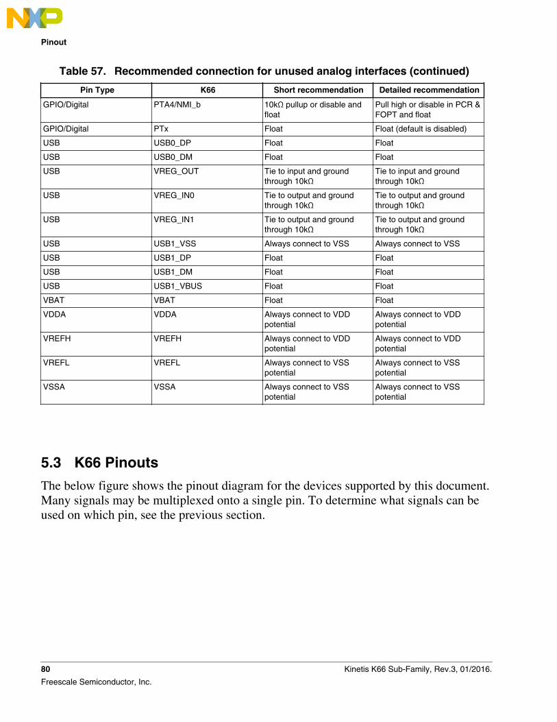
Table 57. Recommended connection for unused analog interfaces (continued)
Pin Type K66 Short recommendation Detailed recommendation
GPIO/Digital PTA4/NMI_b 10kΩ pullup or disable andfloat
Pull high or disable in PCR &FOPT and float
GPIO/Digital PTx Float Float (default is disabled)
USB USB0_DP Float Float
USB USB0_DM Float Float
USB VREG_OUT Tie to input and groundthrough 10kΩ
Tie to input and groundthrough 10kΩ
USB VREG_IN0 Tie to output and groundthrough 10kΩ
Tie to output and groundthrough 10kΩ
USB VREG_IN1 Tie to output and groundthrough 10kΩ
Tie to output and groundthrough 10kΩ
USB USB1_VSS Always connect to VSS Always connect to VSS
USB USB1_DP Float Float
USB USB1_DM Float Float
USB USB1_VBUS Float Float
VBAT VBAT Float Float
VDDA VDDA Always connect to VDDpotential
Always connect to VDDpotential
VREFH VREFH Always connect to VDDpotential
Always connect to VDDpotential
VREFL VREFL Always connect to VSSpotential
Always connect to VSSpotential
VSSA VSSA Always connect to VSSpotential
Always connect to VSSpotential
5.3 K66 Pinouts
The below figure shows the pinout diagram for the devices supported by this document.Many signals may be multiplexed onto a single pin. To determine what signals can beused on which pin, see the previous section.
Pinout
80 Kinetis K66 Sub-Family, Rev.3, 01/2016.
Freescale Semiconductor, Inc.
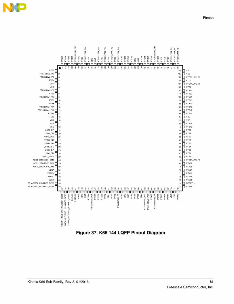
20
19
18
17
16
15
14
13
12
11
10
9
8
7
6
5
4
3
2
1
75
74
73
60595857565554535251 727170696867666564636261
25
24
23
22
21
40393837 50494847464544434241
36
35
34
33
32
31
30
29
28
27
26
99
79
78
77
76
98
97
96
95
94
93
92
91
90
89
88
80
81
82
83
84
85
86
87
100
108 VDD
107
106
105
104
103
102
101
VSS
PTC3/LLWU_P7
PTC2
PTC1/LLWU_P6
PTC0
PTB23
PTB22
116
PT
C11
/LLW
U_P
11
115
114
113
112
111
110
109
PT
C10
PT
C9
PT
C8
PT
C7
PT
C6/
LLW
U_P
10
PT
C5/
LLW
U_P
9
PT
C4/
LLW
U_P
8
124
PT
C17
123
122
121
120
119
118
117
PT
C16
VD
D
VS
S
PT
C15
PT
C14
PT
C13
PT
C12
132
PT
D5
131
130
129
128
127
126
125
PT
D4/
LLW
U_P
14
PT
D3
PT
D2/
LLW
U_P
13
PT
D1
PT
D0/
LLW
U_P
12
PT
C19
PT
C18
140
PT
D11
/LLW
U_P
25
139
138
137
136
135
134
133
PT
D10
PT
D9
PT
D8/
LLW
U_P
24
PT
D7
VD
D
VS
S
PT
D6/
LLW
U_P
15
144
143
142
141
PT
D15
PT
D14
PT
D13
PT
D12
PTB20
PTA28
PTA27
PTA26
PTA25
PTB19
PTB18
PTB17
PTB16
VDD
VSS
PTB11
PTB10
PTB9
PTB8
PTB7
PTA29
PTB0/LLWU_P5
PTB1
PTB2
PTB3
PTB4
PTB5
PTB6
PTB21
PTA24
RESET_b
PTA19
PTA
18
VS
S
VD
D
PTA
17
PTA
16
PTA
15
PTA
14
PTA
13/L
LWU
_P4
PTA
12
PTA
11/L
LWU
_P23
PTA
10/L
LWU
_P22
PTA
9
PTA
8
PTA
7
PTA
6
VS
S
VD
D
PTA
5
PTA
4/LL
WU
_P3
PTA
3
PTA
2
PTA
1
PTA
0
PT
E28
PT
E27
PT
E26
PT
E25
/LLW
U_P
21
PT
E24
VS
S
VD
D
VB
AT
EX
TAL3
2
XTA
L32
DA
C1_
OU
T/C
MP
0_IN
4/C
MP
2_IN
3/A
DC
1_S
E23
DA
C0_
OU
T/C
MP
1_IN
3/A
DC
0_S
E23
VR
EF
_OU
T/C
MP
1_IN
5/C
MP
0_IN
5/A
DC
1_S
E18
USB0_DM
USB0_DP
VSS
VSS
VDD
PTE12
PTE11
PTE10/LLWU_P18
PTE9/LLWU_P17
PTE8
PTE7
PTE6/LLWU_P16
PTE5
PTE4/LLWU_P2
VSS
VDD
PTE3
PTE2/LLWU_P1
PTE1/LLWU_P0
PTE0
USB1_DP
USB1_VSS
VREG_IN1
VREG_IN0
VREG_OUT
ADC0_SE16/CMP1_IN2/ADC0_SE21
ADC1_SE16/CMP2_IN2/ADC0_SE22
VSSA
VREFL
VREFH
VDDA
ADC1_DM0/ADC0_DM3
ADC1_DP0/ADC0_DP3
ADC0_DM0/ADC1_DM3
USB1_VBUS
USB1_DM
Figure 37. K66 144 LQFP Pinout Diagram
Pinout
Kinetis K66 Sub-Family, Rev.3, 01/2016. 81
Freescale Semiconductor, Inc.
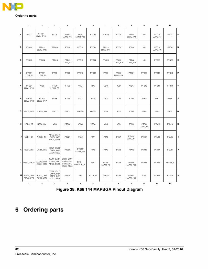
1 2 3 4 5 6 7 8 9
1 2 3 4 5 6 7 8 9
A
B
C
D
E
F
G
H
J
A
B
C
D
E
F
G
H
J
10
KK
10
11
11
LL
12
12
MM PTA18
PTC8 PTC4/LLWU_P8
NC PTC3/LLWU_P7
PTC2
PTA1 PTA6PTA0PTE27ADC0_SE16/CMP1_IN2/ADC0_SE21
ADC1_SE16/CMP2_IN2/ADC0_SE22
PTE26 PTE25/LLWU_P21
PTA2 PTA3 PTA8
PTA7
VSSVSSVSSAVDDAPTE28VSSUSB0_DM
VREG_IN1
USB1_VSS
ADC0_DM0/ADC1_DM3
DAC0_OUT/CMP1_IN3/ADC0_SE23
DAC1_OUT/CMP0_IN4/CMP2_IN3/ADC1_SE23
RTC_WAKEUP_B
VBAT PTA4/LLWU_P3
PTA9 PTA11/LLWU_P23
PTA12
PTA13/LLWU_P4
PTB1
PTA27
PTB0/LLWU_P5
PTB4PTB5VSSVSSVREFLVREFHPTE11PTE12VREG_IN0VREG_OUT
USB0_DP
USB1_DP
USB1_DM
USB1_VBUS
ADC1_DP0/ADC0_DP3
ADC1_DM0/ADC0_DM3
VREF_OUT/CMP1_IN5/CMP0_IN5/ADC1_SE18
PTE24 NC EXTAL32 XTAL32 PTA5 PTA10/LLWU_P22
VSS
PTA16
PTA14
PTB3
PTA29
PTA26
PTA17
PTA15
PTA19
RESET_b
PTA24
PTA25
PTA28
PTB2
PTB6PTB7PTB8PTB9VDD
VDD PTB17 PTB16 PTB10PTB11
PTB19 PTB18
PTB22PTB23NC
PTB20PTB21PTC5/LLWU_P9
PTD8/LLWU_P24
PTC6/LLWU_P10
PTC7 PTD9 NC PTC1/LLWU_P6
PTC0
VSS VSS
VDDVDD
PTC13 PTC9
PTC11/LLWU_P11
PTC10
PTC19 PTC15
PTC14PTC18PTD2/LLWU_P13
PTD3PTD10
PTD13
PTE0 PTD1 PTC17
VDD
VDDPTE7
PTE3PTE4/LLWU_P2
PTE8PTE9/LLWU_P17
PTE10/LLWU_P18
PTE6/LLWU_P16
PTE5
PTE1/LLWU_P0
PTE2/LLWU_P1
PTD15 PTD14
PTD11/LLWU_P25
PTD12
PTC12PTC16PTD0/LLWU_P12
PTD4/LLWU_P14
PTD5PTD6/LLWU_P15
PTD7
Figure 38. K66 144 MAPBGA Pinout Diagram
6 Ordering parts
Ordering parts
82 Kinetis K66 Sub-Family, Rev.3, 01/2016.
Freescale Semiconductor, Inc.
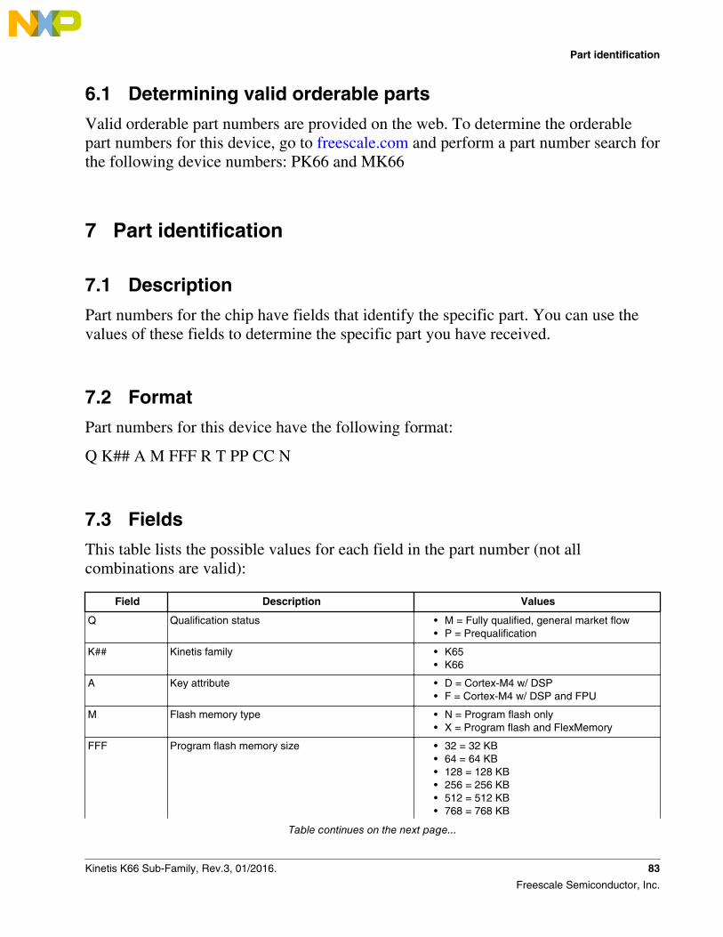
6.1 Determining valid orderable parts
Valid orderable part numbers are provided on the web. To determine the orderablepart numbers for this device, go to freescale.com and perform a part number search forthe following device numbers: PK66 and MK66
7 Part identification
7.1 Description
Part numbers for the chip have fields that identify the specific part. You can use thevalues of these fields to determine the specific part you have received.
7.2 Format
Part numbers for this device have the following format:
Q K## A M FFF R T PP CC N
7.3 Fields
This table lists the possible values for each field in the part number (not allcombinations are valid):
Field Description Values
Q Qualification status • M = Fully qualified, general market flow• P = Prequalification
K## Kinetis family • K65• K66
A Key attribute • D = Cortex-M4 w/ DSP• F = Cortex-M4 w/ DSP and FPU
M Flash memory type • N = Program flash only• X = Program flash and FlexMemory
FFF Program flash memory size • 32 = 32 KB• 64 = 64 KB• 128 = 128 KB• 256 = 256 KB• 512 = 512 KB• 768 = 768 KB
Table continues on the next page...
Part identification
Kinetis K66 Sub-Family, Rev.3, 01/2016. 83
Freescale Semiconductor, Inc.
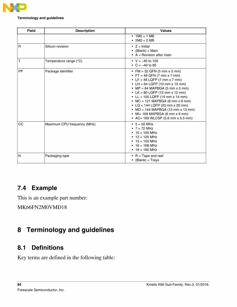
Field Description Values
• 1M0 = 1 MB• 2M0 = 2 MB
R Silicon revision • Z = Initial• (Blank) = Main• A = Revision after main
T Temperature range (°C) • V = –40 to 105• C = –40 to 85
PP Package identifier • FM = 32 QFN (5 mm x 5 mm)• FT = 48 QFN (7 mm x 7 mm)• LF = 48 LQFP (7 mm x 7 mm)• LH = 64 LQFP (10 mm x 10 mm)• MP = 64 MAPBGA (5 mm x 5 mm)• LK = 80 LQFP (12 mm x 12 mm)• LL = 100 LQFP (14 mm x 14 mm)• MC = 121 MAPBGA (8 mm x 8 mm)• LQ = 144 LQFP (20 mm x 20 mm)• MD = 144 MAPBGA (13 mm x 13 mm)• MI= 169 MAPBGA (9 mm x 9 mm)• AC= 169 WLCSP (5.6 mm x 5.5 mm)
CC Maximum CPU frequency (MHz) • 5 = 50 MHz• 7 = 72 MHz• 10 = 100 MHz• 12 = 120 MHz• 15 = 150 MHz• 16 = 168 MHz• 18 = 180 MHz
N Packaging type • R = Tape and reel• (Blank) = Trays
7.4 Example
This is an example part number:
MK66FN2M0VMD18
8 Terminology and guidelines
8.1 Definitions
Key terms are defined in the following table:
Terminology and guidelines
84 Kinetis K66 Sub-Family, Rev.3, 01/2016.
Freescale Semiconductor, Inc.
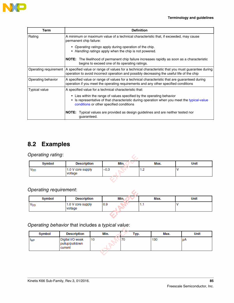
Term Definition
Rating A minimum or maximum value of a technical characteristic that, if exceeded, may causepermanent chip failure:
• Operating ratings apply during operation of the chip.• Handling ratings apply when the chip is not powered.
NOTE: The likelihood of permanent chip failure increases rapidly as soon as a characteristicbegins to exceed one of its operating ratings.
Operating requirement A specified value or range of values for a technical characteristic that you must guarantee duringoperation to avoid incorrect operation and possibly decreasing the useful life of the chip
Operating behavior A specified value or range of values for a technical characteristic that are guaranteed duringoperation if you meet the operating requirements and any other specified conditions
Typical value A specified value for a technical characteristic that:
• Lies within the range of values specified by the operating behavior• Is representative of that characteristic during operation when you meet the typical-value
conditions or other specified conditions
NOTE: Typical values are provided as design guidelines and are neither tested norguaranteed.
8.2 Examples
Operating rating:
Operating requirement:
Operating behavior that includes a typical value:
EXAMPLE
EXAMPLE
EXAMPLE
EXAMPLE
Terminology and guidelines
Kinetis K66 Sub-Family, Rev.3, 01/2016. 85
Freescale Semiconductor, Inc.
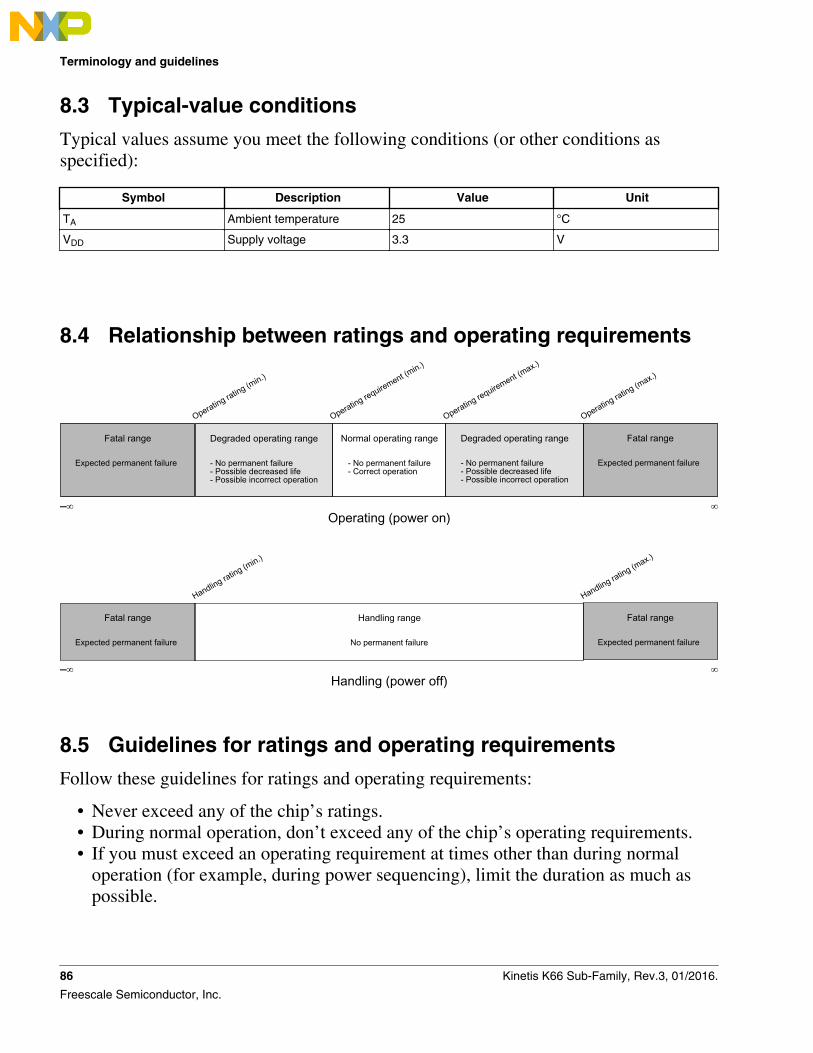
8.3 Typical-value conditions
Typical values assume you meet the following conditions (or other conditions asspecified):
Symbol Description Value Unit
TA Ambient temperature 25 °C
VDD Supply voltage 3.3 V
8.4 Relationship between ratings and operating requirements
–∞
- No permanent failure- Correct operation
Normal operating rangeFatal range
Expected permanent failure
Fatal range
Expected permanent failure
∞
Operating rating (max.)
Operating requirement (max.)
Operating requirement (min.)
Operating rating (min.)
Operating (power on)
Degraded operating range Degraded operating range
–∞
No permanent failure
Handling rangeFatal range
Expected permanent failure
Fatal range
Expected permanent failure
∞
Handling rating (max.)
Handling rating (min.)
Handling (power off)
- No permanent failure- Possible decreased life- Possible incorrect operation
- No permanent failure- Possible decreased life- Possible incorrect operation
8.5 Guidelines for ratings and operating requirements
Follow these guidelines for ratings and operating requirements:
• Never exceed any of the chip’s ratings.• During normal operation, don’t exceed any of the chip’s operating requirements.• If you must exceed an operating requirement at times other than during normal
operation (for example, during power sequencing), limit the duration as much aspossible.
Terminology and guidelines
86 Kinetis K66 Sub-Family, Rev.3, 01/2016.
Freescale Semiconductor, Inc.
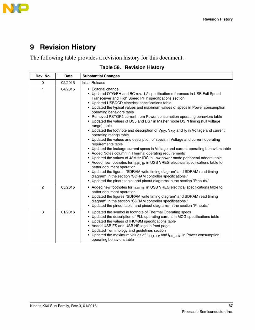
9 Revision HistoryThe following table provides a revision history for this document.
Table 58. Revision History
Rev. No. Date Substantial Changes
0 02/2015 Initial Release
1 04/2015 • Editorial change• Updated OTG/EH and BC rev. 1.2 specification references in USB Full Speed
Transceiver and High Speed PHY specifications section• Updated USBDCD electrical specifications table• Updated the typical values and maximum values of specs in Power consumption
operating behaviors table• Removed PSTOP2 current from Power consumption operating behaviors table• Updated the values of DS5 and DS7 in Master mode DSPI timing (full voltage
range) table• Updated the footnote and description of VDIO, VAIO and ID in Voltage and current
operating ratings table• Updated the values and description of specs in Voltage and current operating
requirements table• Updated the leakage current specs in Voltage and current operating behaviors table• Added Notes column in Thermal operating requirements• Updated the values of 48MHz IRC in Low power mode peripheral adders table• Added new footnotes for IINRUSH in USB VREG electrical specifications table to
better document operation.• Updated the figures "SDRAM write timing diagram" and SDRAM read timing
diagram" in the section "SDRAM controller specifications."• Updated the pinout table, and pinout diagrams in the section "Pinouts."
2 05/2015 • Added new footnotes for IINRUSH in USB VREG electrical specifications table tobetter document operation.
• Updated the figures "SDRAM write timing diagram" and SDRAM read timingdiagram" in the section "SDRAM controller specifications."
• Updated the pinout table, and pinout diagrams in the section "Pinouts."
3 01/2016 • Updated the symbol in footnote of Thermal Operating specs• Updated the description of PLL operating current in MCG specifications table• Updated the values of IRC48M specifications table• Added USB FS and USB HS logo in front page• Updated Terminology and guidelines section• Updated the maximum values of IDD_LLS2 and IDD_LLS3 in Power consumption
operating behaviors table
Revision History
Kinetis K66 Sub-Family, Rev.3, 01/2016. 87
Freescale Semiconductor, Inc.
How to Reach Us:
Home Page:freescale.com
Web Support:freescale.com/support
Information in this document is provided solely to enable system andsoftware implementers to use Freescale products. There are no expressor implied copyright licenses granted hereunder to design or fabricateany integrated circuits based on the information in this document.Freescale reserves the right to make changes without further notice toany products herein.
Freescale makes no warranty, representation, or guarantee regardingthe suitability of its products for any particular purpose, nor doesFreescale assume any liability arising out of the application or use ofany product or circuit, and specifically disclaims any and all liability,including without limitation consequential or incidental damages.“Typical” parameters that may be provided in Freescale data sheetsand/or specifications can and do vary in different applications, andactual performance may vary over time. All operating parameters,including “typicals,” must be validated for each customer application bycustomer's technical experts. Freescale does not convey any licenseunder its patent rights nor the rights of others. Freescale sells productspursuant to standard terms and conditions of sale, which can be foundat the following address: freescale.com/SalesTermsandConditions.
Freescale, the Freescale logo, and Kinetis are trademarks of FreescaleSemiconductor, Inc., Reg. U.S. Pat. & Tm. Off. All other product orservice names are the property of their respective owners. ARM, theARM Powered logo and Cortex are registered trademarks of ARMLimited (or its subsidiaries) in the EU and/or elsewhere. The USB-IFLogo is a registered trademark of USB Implementers Forum, Inc. Allrights reserved.
© 2016 Freescale Semiconductor, Inc.
Document Number K66P144M180SF5V2Revision 3, 01/2016