Embed Size (px)
Citation preview

Keysight Technologies M9195B PXIe Digital Stimulus/Response with PPMU: 250 MHz, 16-channel
Data Sheet

02 | Keysight | M9195B PXIe Digital Stimulus/Response with PPMU: 250 MHz, 16-channel - Data Sheet
Overview
Experience high speed digital test capabilities at a whole new level. The Keysight Technologies, Inc. M9195B PXIe Digital Stimulus/Response (PXI DSR) module is ideal for IC design validation and production test environments. It goes beyond providing just standard capabilities. The new 16-channel, single slot PXI module introduces a high performance pattern cyclizer for powerful pattern creation including advanced timing capabilities such as multiple drive edges per cycle. This provides flexible edge placement and stimulus/response delays for timing margin testing or cable length compensation. Additionally, it can support up to four independent multi-sites with an independent sequencer for each site.
Software tools included with the M9195B allow the user to modify vector and pattern parameters without requiring the user to recompile and download tests. An optional set of digital development tools are also available. These software tools include a graphical pattern editor and pattern conversion tools to speed test development by enabling test patterns from various EDA systems to be read in, edited, and output to the M9195B. Additonal ATE features include:
– High speed pattern application and RZ (Return-to-Zero) clock rate up to 250 MHz – Per pin programming of voltage levels – Real time compare, parametric measurement unit (PPMU) – Deep vector memory and flexible pattern sequencing
With the PXI DSR module you can easily emulate standard serial interfaces like the MIPI® RF Front-End interface or proprietary parallel device interfaces. The test development software tools enable you to quickly create and edit waveform patterns or to import patterns created by automatic test generation applications.
Applications
– RFFE bus emulation used in PA/FEM semiconductor device verification or production test
– Wireless communication devices using parallel or serial digital control – Automated test in product validation or manufacturing test – Backplane emulation for device, board, or module testing – Digital serial and parallel applications
Key features
– Combine modules to form systems of up to 192 channels (requires option MMS). – 16 bidirectional channels with per-pin programmable logic levels – Highly flexible, per-bit timing control for fast and accurate waveform development – Reconfigurable per-pin Parametric Measurement Unit (PPMU) for each channel – Single and multi-site configurations – Edit patterns on-the-fly without recompiling and downloading the test – Execute patterns in arbitrary order – Flexible allocation of deep pattern memory per channel or per site to allocate
memory where it is needed – Channel delay adjustment to compensate for cable and fixture propagation delays – 4 high voltage channels for flash programming or fuse test – 4 open drain auxillary output pins for fixture relays – Hardware triggers and markers for test system synchronization – Comprehensive software tool set for quick test development

03 | Keysight | M9195B PXIe Digital Stimulus/Response with PPMU: 250 MHz, 16-channel - Data Sheet
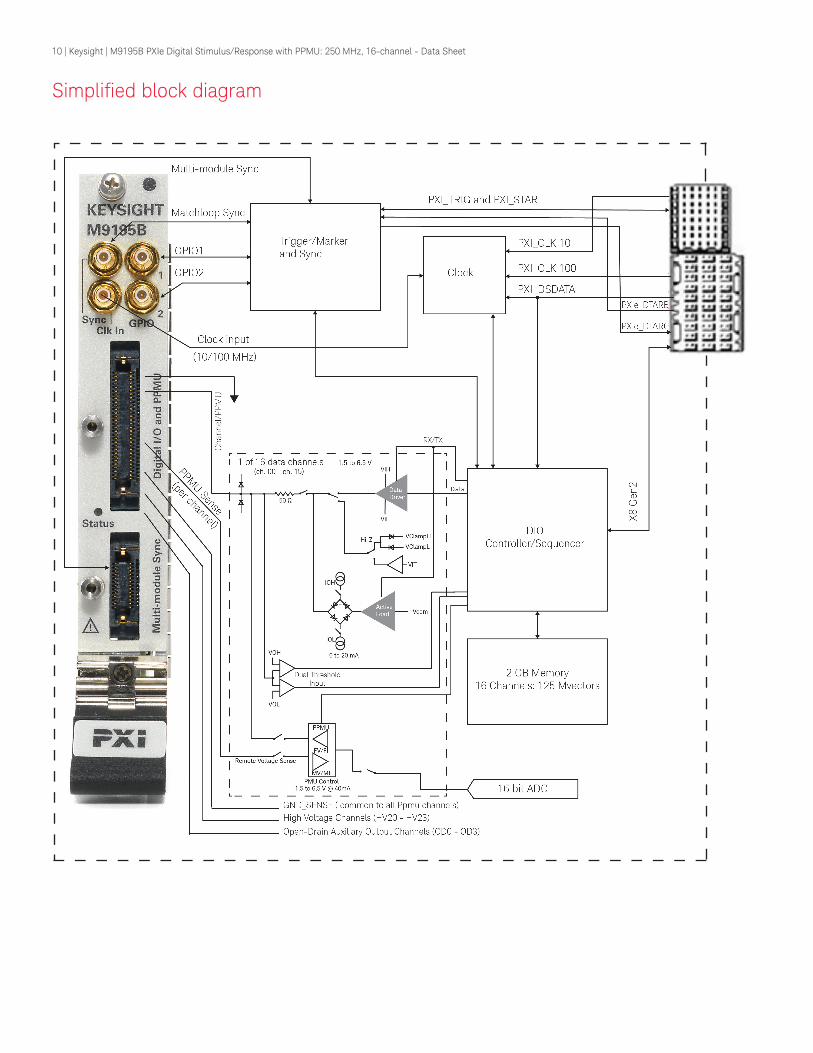
M9195B hardware overview
Individual channel capabilityEach of the 16 bidirectional channels provide programmable logic levels of –1.5 V to +6.5 V with 152 μV resolution. The per channel 4 quadrant parametric measurement unit (PPMU) enables FVMI, FIMV, FVMV, and FIMI and FNMV modes. With the 5 PPMU current ranges between ±2 μA to ±40 mA, users can make accurate leakage measurements.
Each channel can be configured for parametric measurements, as a static digital I/O pin, or with synchronized cyclized digital data. Digital channel direction and timing can be flexibly controlled on a per digital vector basis. The cyclized data allows each pin to operate in RZ or NRZ modes. In combination with the 1 ns edge placement resolution, each pin allows for an adjustable output delay, for timing margin testing, and receive delay to compensate for cabling propagation delays.
Multi-site capability The PXI DSR provides a choice of a single-site configuration with 16 synchronized channels, or a multi-site configuration with 4 sets of 4 synchronized channels. In multi-site mode, each site has its own independent sequencer. This enables site independent clock operation for simultaneous testing. The multi-site capability simplifies test development. Instead of forcing the test engineer to create a single test that encompasses all for sites simultaneously, the user only needs to focus on a single device. The single device test can be easily replicated for the remaining test sites. In addition to the digital pins, each site has a high voltage drive channel and an open drain control channel for relay control.
Multi-module synchronizationUp to 12 modules can be combined to build systems up to 192 channels (requires opt MMS for each module plus the appropriate sync cable, either Y1250A or Y1251A). When modules are combined, they operate in single-site mode and all channels are synchronized to a single test sequencer. Typical channel-to-channel skew (including across modules) is ±300 ps. Multiple modules are combined and programmed together into a single multi-module instrument.
Per-Pin Parametric Measurement Unit (PPMU)The PPMU feature, available on each of the PXI DSR’s 16 channels, enables DC current and voltage measurements. Each channel can be independently programmed to force a voltage and measure the corresponding current, or force a current and measure the voltage. The PPMU can make leakage current measurements at low current ranges or for measuring low input resistance in high current ranges. In a force voltage/measure current (FVMI) mode the PPMU can measure input bias current on a single DUT pin. For high current applications, each channel has remote sense capability to account for the voltage drop across the connecting cable.
Perform continuity testing of a DUT by forcing current into the pin with other DUT pins grounded while measuring the voltage at the pin (FIMV). The FNMV mode (Force Nothing, Measure Voltage) enables the PPMU to be used as a scanning voltmeter. The PPMU provides built-in 64 sample, 50 Hz or 60 Hz averaging to improve measurement quality by rejecting power line noise. All PPMU channels share a 16-bit measurement subsystem for fast accurate measurements.

04 | Keysight | M9195B PXIe Digital Stimulus/Response with PPMU: 250 MHz, 16-channel - Data Sheet
Flexible digital pattern generation With the included software tools, easily create, modify and reuse previously defined patterns. Pattern timing is controlled using up to 32 waveform tables. Within the waveform table, each of the 15 user-defined vector characters is translated into one of the following hardware actions: Force High/Low (U/D), Force to previous state (P), Stop Forcing (Z), Compare High/Low (H/L), Compare to Tri-state (T), Don’t Compare (X). Each vector period has two drive edges that are used when forcing a digital state and one receive edge used to compare digital data from the DUT. Edge placement resolution can be set as low as 1 ns and edge placement can vary from period to period so that oversampling is not required. The two drive edges enable the user to easily create a clock or other RZ formats from a single vector without requiring two vectors. The flexibility of the drive edges allow them to be changed on a per vector basis using the vector characters or by referencing a different waveform table.
The combination of the waveform tables and edge placement resolution simplifies the pattern programming. Variables and equations can be defined to allow the user to simultaneously modify timing relationships and edge placement.
Once compiled, the digital patterns are stored in the PXI DSR’s on-board pattern cache. The PXI DSR executes the patterns from the cache in order to provide high test throughput. High-level pattern sequencing commands allow for high level macros which can be used to define timing sets, counted and uncounted looping of pattern blocks, conditional execution based upon matching parallel or serial patterns, or wait for software trigger advance.
Advance timing capabilities Change pattern values that have been downloaded to the cache without recompiling. Pattern values can replace either parallel vectors or serial patterns. These powerful features allow you to quickly modify patterns directly from the API. The user can create pattern templates that are used to read or write to the DUT, then provide the vector information directly from the API.
Variables can be modified at the API level without recompiling the test pattern. This allows the user to control pattern timing or levels directly from the API. These advanced capabilities useful for test applications such as a timing or voltage level shmoo.
Serial and parallel digital bus emulationThe combination of the flexible pattern timing and sequencing features, enables the PXI DSR to emulate a wide variety of standard or custom serial/parallel protocols such as SPI and RFFE.

05 | Keysight | M9195B PXIe Digital Stimulus/Response with PPMU: 250 MHz, 16-channel - Data Sheet
Comprehensive software tool set
Keysight offers a choice of drivers and programming environments to configure and control the PXI DSR during test development including:
– Full featured, high-level IVI-COM, IVI-C, LabVIEW programming interfaces through drivers
– IEEE-1450/ STIL, OpenXML (Excel), or text file format for programmatically defining patterns
– The M9195B Soft Front Panel for interactive test control and debug – The M9192A/M9193A DSR pattern editor and data converters software enable test
patterns from various EDA systems to be read in, edited, and output to the M9195B
These test development tools can be used in powerful combinations to match the DUT’s test flow and test requirements.
Soft Front Panel (SFP)The SFP assists the user in the development and application of test patterns, allows the user to change key test execution parameters, and allows the user to validate and compensate for test fixture connectivity. During pattern development, the user interactively loads and execute STIL, XML, or bulk data files. When loading, the tests are checked for correct syntax and the SFP generates error messages to help debug patterns. The SFP enables the user to the control various execution and response logging modes. In addition to these features, the SFP uses the same IVI interface driver calls. Each function initiated by the SFP logs an example driver call that can then be used in a regular API environment.
IVI and LabVIEW driversThe IVI driver set can be used to fully control all aspects of test development using the DSR from assigning hardware pins to creating and executing waveform patterns using the M9195B. The drivers include high level commands for:
– Initial configuration including pin/channel names assignments, signal direction, grouping pins/channels to make vector definition easier.
– Setting physical layer conditions such as voltage levels, active loads – Defining single or multisite configurations. – Pattern definition and waveform timing. – Pattern sequencing

06 | Keysight | M9195B PXIe Digital Stimulus/Response with PPMU: 250 MHz, 16-channel - Data Sheet
Standard Test Interface Language (STIL) SupportThe PXI DSR takes advantage of the Standard Test Interface language (STIL) IEEE Std 1450.0 which was designed for ATE testing. The PXI DSR can be configured using STIL commands that specify signal grouping, patterns, format, and timing information used to apply digital test vectors to a device being tested. Using a simple text editor and using the STIL format, attributes needed to generate digital patterns can quickly be created. STIL tests are easy to read and understand which simplifies test development and debug. Either the IVI API or the SFP can execute tests developed in STIL.
Bulk data importThe PXI DSR supports bulk data file import to load legacy and tool generated patterns. Bulk data import utilizes simple text files where the first row contains signal names and provides the option to a reference a waveform table. Each subsequent row represents the vectors which make up the patterns. The waveform table itself can be defined using the SFP, IVI driver, or STIL file. This provides a quick and easy way to develop production tests using patterns developed in R&D.

07 | Keysight | M9195B PXIe Digital Stimulus/Response with PPMU: 250 MHz, 16-channel - Data Sheet
XML (.xlsx) programming interfaceThe XML interface allows the user to develop and debug tests in a spreadsheet form. The STIL methodology fits well with the multiple worksheet concepts provided in modern spreadsheet tools. Each worksheet matches a STIL function such as Signals, Waveform Tables, and Patterns. Digital patterns are tabular in nature and therefore fit very well into a spreadsheet. The spreadsheet provides an easy to use, flexible, and familiar interface for novice or expert users to quickly develop digital tests. All of the standard spreadsheet tools, such as equations, are available to help with pattern creation. This spreadsheet interface can be used to configure and control the M9195B channels and key features is provided as a standard development tool. Spreadsheet tests can be executed using either the SFP or associated IVI commands.

08 | Keysight | M9195B PXIe Digital Stimulus/Response with PPMU: 250 MHz, 16-channel - Data Sheet
M9192A and M9193A DSR Pattern Editor and Data Converter SoftwareThe optional M9192A and M9193A provide a complete set of vector translation and pattern validation software tools for the M9195B. These tools enable design and test engineers to save time, cut costs, and dramatically decrease time to market.
M9192A DSR pattern editor softwareThe M9192A DSR pattern editor, based on the Solstice-TDS WaveMaker+ module from Test Systems Strategies Inc. (TSSI), was customized to support the M9195B. The M9192A includes a DSR STIL In-converter, a DSR STIL Tester Bridge, and M9195B error handling. M9195B STIL files can be read using the In-converter and graphically displayed in the pattern editor. Patterns and timing information can then be edited in a single window. This enables you to generate and validate your own test patterns. The modified digital patterns can then be output as a STIL file utilizing the DSR STIL tester bridge. These STIL files can be loaded directly into the M9195B Soft Front Panel or used programmatically.
The pattern editor also speeds up test debug. M9195B error log files can be dragged-and-dropped into waveform editor. This gives immediate visibility of discrepancies between the expected and actual states of the DUT. The digital waveforms can then be edited to ensure a passing test.

09 | Keysight | M9195B PXIe Digital Stimulus/Response with PPMU: 250 MHz, 16-channel - Data Sheet
M9193A DSR Pattern Editor with Data Converters SoftwareThe M9193A DSR pattern editor with data converters combines the digital pattern editor with data converters based on Solstice-TDS In-converters from TSSI. The M9193A enables the utilization of digital pattern files from various Automatic Test Program Generators (ATPGs). Vector files can be read using an appropriate In-converter and then edited using the pattern editor. In the case of Verilog files, an event-based database without timing is created when the VCE/ECVD file is read, and supplied cyclization tools add timing. Once the digital patterns are complete, they can be utilized by the M9195B via the DSR tester bridge. The resulting digital development environment results in fast test development using ATPGs and customized output for the M9195B DSR.
The M9193A includes the following In-converters:
– The WGL In-converter reads an ASCII file that’s compliant to the TSSI Waveform Generation Language (WGL) Specification.
– The STIL In-converter reads a text file that is STIL specification compliant (IEEE Std 1450.0-1999). This In-converter is very useful for reading files produced by many ATPGs including Synopsys TetraMAX, Cadence Encounter, and Mentor Graphics FastScan. Note: the M9195B PXIe DSR uses an enhanced version of STIL and is not supported with this STIL In-converter. However, the M9195B is supported with the Keysight DSR STIL In-converter that comes standard with the pattern editor.
– The Verilog In-converter converts a Value Change Dump (VCD) or an Extended Value Change Dump (EVCD) file generated by a Verilog simulator (e.g., Cadence IUS, Mentor Questa, or Synopsys VCS).
– The ASCII In-converter is a flexible, tabular form reader. The TSSI ASCII format is a host-independent, human-readable representation of cyclized test patterns. This format is designed for importing a bulk of data. The bulk data can be created from scratch or by converting from a different pattern format as long as it conforms to the TSSI ASCII format specification. Note: this data format is different than the bulk data format used with the M9195B Soft Front panel.
10 | Keysight | M9195B PXIe Digital Stimulus/Response with PPMU: 250 MHz, 16-channel - Data Sheet
Simplified block diagram

11 | Keysight | M9195B PXIe Digital Stimulus/Response with PPMU: 250 MHz, 16-channel - Data Sheet
Accessories and cables are designed for easy, accurate, and reliable digital IO connections
Single-site (16 channels) signal cables – Y1245A (0.5 meter), Y1246A (1 meter), or Y1247A (2 meter) – 60 micro coax lines for 16 digital Ch, 16 PPMU sense Ch, 4 high voltage Ch , and 4
open drain/grounds Ch – Male Edge Rate with squeeze latches or thumb screw hood
Multi-site (4 sites of 4 channels) signal cables – 1248A (1 meter) or Y1249A (2 meter) – 16 Ch divided into 4 independent partitions (connectors) – Each partition contains an Edge Rate connector with squeeze latch, 4 digital Ch, 4
PPMU sense Ch, 1 high voltage Ch, and 1 open drain Ch – 4 alternate thumb screw hoods are also provided for optional use – Requires option S04
Multi-module synchronization cables – Y1250A four module cable or Y1251A twelve module cable – Used to interconnect and synchronize multiple M9195B modules – Only one cable is required per set of M9195B modules – Requires option MMS

12 | Keysight | M9195B PXIe Digital Stimulus/Response with PPMU: 250 MHz, 16-channel - Data Sheet
Evaluation and prototyping board – Y1253A allows users to access individual signal pins
for prototyping or debug. – Board consists of 1 inch of signal header breakout
pins, prototyping area with associated power connector, and signal termination pads.
– Offers 9in2 of bread board area, power/ground, includes headers for 16 channels, 16 PPMU channels high voltage and open drain channels
– The Y1253A proto board is designed for use with the single-site, Y1245A, Y1246A and Y1247A, cables only.
SMA breakout cables – Y1254A (1 meter) and Y1255A (2 meter) – Enables user access to individual signal pins/channels
for prototyping or debug – SMA connectors plus a header for low-speed signals. – Cables work with both the single and multi-site
configurations

13 | Keysight | M9195B PXIe Digital Stimulus/Response with PPMU: 250 MHz, 16-channel - Data Sheet
Definitions for specifications and characteristics
Specifications Warranted performance. Specifications include guardbands to account for the expected statistical performance distribution, measurement uncertainties, and changes in performance due to environmental conditions. All specifications and characteristics apply over the operating environment outlined in “Environmental and Regulatory” section of this data sheet. In addition, the following conditions must be met:
– Instrument has been turned on for 30 minutes with the PXI DSR software running. – Instrument is within its calibration cycle. – Instrument remains at a stable surrounding environment temperature (between 0°C to 45°C) for 1 hour prior to turn-on.
Specifications in this document are identified by an asterisk (*).
Characteristics A performance parameter that the product is expected to meet before it leaves the factory, but that is not verified in the field. A characteristic includes the same guardbands as a specification.
Typical Expected performance of an average unit at a stable temperature between 20°C to 30°C for 30 minutes prior to turn-on and during operation; does not include guardbands. The instrument must be within its calibration cycle.
Nominal A general, descriptive term or design parameter. It is not tested. Data represented in this document are nominal unless otherwise identified.
Best practices To ensure proper cooling, use Keysight slot blockers (Y1212A), filler panels (Y1213A), and the air inlet module kit (Y1214A) in the chassis when there are empty slots. Keysight chassis and filler panels optimize module temperature performance.
At environmental temperatures > 40 °C, chassis fans should be set to high.
Additional information All data are measured from multiple units at room temperature and are representative of product performance within the operating temperature range unless otherwise noted.
The specifications contained in this document are subject to change.
Technical specifications and characteristics
General Characteristics
Module characteristics
Bus interface & compatibility PXI Express peripheral module (x1, x4, x8 PCIe® specification v 2.1)
Number of data channels 16, per-channel parametric measurement unit (PPMU)
Number of sites per module One 16 channel or four 4-channel sites (option dependent)
Maximum data rate for data channels 250 Mbps (option dependent)
Maximum RTZ clock on data channels 250 MHz (option dependent)
Number of high voltage channels 4
Number of auxiliary open drain channels 4
Module memory 2 GB (allocated between pattern, response capture and sequence control)
Maximum number of synchronized modules 12 (requires opt MMS)
Maximum number of synchronized channels 192 (requires opt MMS)
Front panel connectors
Data , open drain, HV, PPMU sense ERCD30
Reference clock input (REF CLK IN) SMB connector
Sync in/out (SYNC) SMB connector
Trigger in/marker out (GPIO1/2) SMB connector
Mechanical characteristics
Dimensions(H x W x D) in mm
3U/1-slot PXIe standard130.1 x 21.7 x 210 mm; includes connector and handle extensions
Weight 482 g

14 | Keysight | M9195B PXIe Digital Stimulus/Response with PPMU: 250 MHz, 16-channel - Data Sheet
Technical specifications and characteristics
DC Power Requirements
DC supply Typical Maximum
DC supply current:
+3.3 V 3.0 A 4.5 A
+12 V 2.8 A 3.2 A
Power dissipation (max) 44 W 53 W
Data Channel Characteristics
Characteristic* denotes warranted specification
Value Comments
Number of data channels 16
Maximum pattern memory 125 Mvectors per channel Option dependent
Channel type Single-ended, ground reference
Channel impedence 50 Ω Nominal
Direction control (In, Out, In/Out) Per channel, per cycle (period)
Per cycle digital states 2 drive states, 1 receive state
Programmable drive states Force high, force low, force terminate Terminate state either drives active termination or is high-Z with reflection clamps
Programmable receive states Compare high, compare low, compare three-state, compare off
Three-state: a signal level between receive high and receive low thresholds
Programmable voltage setting Per channel
Drive/receive voltage range –1.5 V to +6.5 V(16-bit with 152 µV resolution)
VIH − VIL ≥ 100 mVVIL (–1.5 V to +6.4 V)VIH (–1.4 V to +6.5 V)
Drive voltage accuracy * ±25 mV (VIH & VIL)DUT centric
DUT centric. Maximum accuracy from ±5 °C of AutoCorrections
Receive voltage accuracy * ±20 mV (VOH & VOL)DUT centric
DUT centric. Hysteresis off. Maximum accuracy from ±5 °C of AutoCorrections
Channel output short circuit current limit ±75 mA, nominal Maximum of 250 mA per module in combination with other channels
Channel rise time <450 ps @ 1 V pp (programmed) <700 ps @ 3 V pp (programmed) <1250 ps @ 6 V pp (programmed)
Into 50 Ω, 20-80%, typical
Channel fall time <450 ps @ 1 V pp (programmed) <700 ps @ 3 V pp (programmed) <1250 ps @ 6 V pp (programmed)
Into 50 Ω, 20-80%, typical
Minimum detectable voltage swing, receive
40 mV Nominal. Hysteresis off
High impedance current leakage – Receive-only channel – Receive-only, low leakage mode * – Bi-directional channel
±6 nA±1.5 nA±2 μA
Typical. Static or dynamic digital modeDynamic digital mode only 1
Typical. Static or dynamic digital mode
Channel power-on state high-Z
Receive hysteresis settings 0 mV, 50 mV, 100 mV
Channel jitter <25 ps RMS Typical. EPR 2 = 1 ns
Channel to channel jitter <25 ps RMS Typical. EPR 2 = 1 ns
1. The following conditions apply: 0 °C - 30 °C operating range, ±2 °C of measure leakage current, 250 mV of measure leakage voltage (±1 V range)2. EPR = Edge Placement Resolution

15 | Keysight | M9195B PXIe Digital Stimulus/Response with PPMU: 250 MHz, 16-channel - Data Sheet
Data Channel Characteristics
Characteristic* denotes warranted specification
Value Comments
Active termination range –1.5 V to +6.5 V(16-bit with 152 µV resolution)
50 Ω terminated into VIT
Active termination accuracy * ±25 mV (VIT) Maximum accuracy from ±5 °C of AutoCorrections
Reflection clamp range –2 V to +7 V(16-bit with 152 µV resolution)
VCH − VCL > 0.8 VVCL (–2 V to +6.2 V)VCH (–1.2 V to +7 V)
Reflection clamp accuracy ±30 mV @ 1 mA (VCH & VCL)±200 mV @ 10 mA (VCH & VCL)±400 mV @ 25 mA (VCH & VCL)
50 Ω source impedence into clamps. Characteristic accuracy from ±5 °C of AutoCorrections neglecting source impedence voltage drop
Active load range (IOH & IOL) 0 mA to 25 mA(16-bit with 762 nA resolution)
Maximum of 250 mA per module in combination with other channels
Active load accuracy ±0.40 mA (IOH & IOL) Characteristic accuracy from ±5 °C of AutoCorrections
Commutation voltage range –1.5 V to +6.5 V–1 V to +5.5 V
| IOL & IOH | ≤ 1 mA| IOL & IOH | ≤ 25 mA
Commutation voltage accuracy ±20 mV (VCOM) Characteristic accuracy from ±5 °C of AutoCorrections
High Voltage Channel Characteristics
Characteristic* denotes warranted specification
Value Comments
Number of high voltage channels 4
Channel type Single-ended, ground referenced
Channel control Shared with dependent data channel Refer to user manual for HV control informationHV20 shared with CH 02HV21 shared with CH 06HV23 shared with CH 10HV24 shared with CH 14
Channel impedence <10 Ω (when forcing to terminate) 50 Ω (when forcing High or Low)
Nominal
Channel power-on state Passive 50 Ω termination
Maximum data rate 10 MHz
Programmable voltage range setting Per channel
HV drive range 0 V to +13.5 V(16-bit with 305 µV resolution)
Force terminate
HV drive accuracy * ±40 mV (VHH) Maximum accuracy from ±5 °C of AutoCorrections
Drive voltage range –0.1 V to +6.5 V(16-bit with 152 µV resolution)
Force high or low
Drive voltage accuracy * ±35 mV (VIH & VIL) Maximum accuracy from ±5 °C of AutoCorrections
HV drive settling time < 4 µs @ 13.5 V pp into 1 M Ω (1nF)< 350 µs @ 13.5 V pp into 1 M Ω (1nF)
Settled to 1% of final valueTypical
HV channel short circuit current limit ±60 mA, nominal Maximum of 250 mA per module in combination with other channels. Nominal
Technical specifications and characteristics

16 | Keysight | M9195B PXIe Digital Stimulus/Response with PPMU: 250 MHz, 16-channel - Data Sheet
Open Drain Channel Characteristics
Characteristic Value Comments
Number of auxiliary open drain channels 4
Channel type Output only, single-ended, ground referenced
Channel termination Open drain Internal 10k Ω pull-up to +5 V
Sink current per channel 1 A max Nominal
Channel power-on state Off 10k Ω pull-up to +5 V
Maximum working voltage + 12 Vdc
Technical specifications and characteristics
High Voltage Channel Characteristics
Characteristic* denotes warranted specification
Value Comments
Drive rise time <9 ps @ 1 V pp (programmed) <10 ps @ 3 V pp (programmed) <11 ps @ 6 V pp (programmed)
Into 50 Ω, 20-80%, Typical
Drive fall time <9 ps @ 1 V pp (programmed) <10 ps @ 3 V pp (programmed) <11 ps @ 6 V pp (programmed)
Into 50 Ω, 20-80%, Typical
Drive source/sink current per channel ±60 mA, nominal Maximum of 250 mA per module in combination with other channels
GP-IO Characteristics
Characteristic* denotes warranted specification
Value Comments
Number GP-IO channels 2 Trigger In/Marker Out (GPIO 1/2 SMB)
Channel type Single ended, ground referenced
Direction control Per channel
Channel input impedance 50 Ω or 10 kΩ Software selectable, DC coupled
Programmable polarity Positive or negative slope
Programmable threshold setting Per channel
Input voltage range –2 to + 5 V
Programmable input threshold –2 to + 5 V
Input threshold accuracy ±100 mV 10 kΩ input impedance
Input minimum pulse width 16 ns
Input rate DC to 30 MHz
Channel output impedance 50 Ω Marker
Output voltage 3.3 V max (into high-Z)1.65 V max (into 50 Ω)
Nominal
Output rate DC to 100 MHz
Output rise / fall time <3 ns Typical into 50 Ω, 20%-80%
Source/sink current per channel ± 64 mA Nominal

17 | Keysight | M9195B PXIe Digital Stimulus/Response with PPMU: 250 MHz, 16-channel - Data Sheet
Technical specifications and characteristics
PPMU Characteristics
Characteristic* denotes warranted specification
Value Comments
Number of PPMU channels 16
PPMU modes Force V measure V, Force V measure I, Force I measure I, Force I measure V, Force nothing measure V
Measurement averaging modes None, 64 averages, 50 Hz one PLC, 60 Hz one PLC
Force voltage range –2 V to +6.5 V (| Current | ≤ 4 mA)–2 V to +6 V (| Current | ≤ 25 mA)–2 V to +5.75 V (| Current | ≤ 40 mA)(16-bit with 152 µV resolution)
Force voltage accuracy * ±10 mV Maximum accuracy from ±5 °C of AutoCorrections. Ground sense tied to ground.
Measure voltage accuracy * ±10 mV With remote sense. Maximum accuracy from ±5 °C of AutoCorrections with one PLC averaging at sense location. Ground sense tied to ground
Force voltage settling time < 20 µS (40 mA range)< 20 µS (1 mA range)< 25 µS (100 µA range)< 100 µS (10 µA range)< 525 µS (2 µA range)
1 V rising and falling step settled to 1% of final value into 1 MΩ/ 1nF load. Typical
Force voltage stability Stable at all ranges into 1 µF Larger load capacitance possible, but response limited by current slew rate.
Current range –40 mA to + 40 mA(16-bit with 2.44 µA resolution)
Maximum of 250 mA per module in combination with other channels
–1 mA to + 1 mA(16-bit with 61 nA resolution)
–100 µA to + 100 µA(16-bit with 6.1 nA resolution)
–10 µA to + 10 µA(16-bit with 610 pA resolution)
–2 µA to + 2 µA(16-bit with 122 pA resolution)
Force current accuracy * ±1% of range Maximum accuracy from ±5 °C of AutoCorrections. Remote sense disconnected.
Measure current accuracy * ±1% of range Maximum accuracy from ±5 °C of AutoCorrections with one PLC averaging. Remote sense disconnected.
Force current settling time Dependent on load
Channel leakage ±10 nA Typical
Remote sense 16 channels1 GND
Ground sense should be tied to ground at measurement location for maximum accuracy.
Remote sense leakage ±4 nA Typical
Force current voltage clamp range –2 V to +6.5 V(16-bit with 152 µV resolution)
VCH > VCLVCL (–2 V to +4 V)VCH (0 V to +6.5 V)
Force current voltage clamp accuracy ±50 mV Characteristic accuracy from ±5 °C of AutoCorrections

18 | Keysight | M9195B PXIe Digital Stimulus/Response with PPMU: 250 MHz, 16-channel - Data Sheet
Timing and Trigger Characteristics
Channel clock
Number of independent clock domains 1 - when configured as a single, 16 channel site4 - when configured as 4, 4 channel sites
Number of independent clocks depends on the number of sites selected and option
Maximum RZ clock rate on a data channel 250 MHz (option dependent)
Minimum RZ clock rate on a data channel 5 mHz
Clock jitter <25 ps RMS
Internal reference clock
Frequency 100 MHz
Accuracy ±25 ppm
Period jitter <2 ps RMS
Reference clock sources PXI_CLK100, PXIe-DSTARA, CLK IN
External reference clock input (SMB front panel)
Input frequency 10 MHz or 100 MHz
Input impedance (CLK IN) 50 Ω Nominal, AC coupled
Input voltage range (CLK IN) +1.8 V to + 3.3 V
Lock range accuracy ±25 ppm
Duty cycle 40 to 60%
Channel timing (per channel)
Waveform timing change Per vector
Edge placement resolution (EPR) 1 ns minimum Dependent on waveform table period
Stimulus delay resolution per test: Edge Placement Resolution (EPR) isspecified at the time of test activation. – For EPR ≥ 1 ns and ≤ 1.3 ns
– For EPR > 1.3 ns 24 psEPR
Stimulus delay range per test 254 x EPR
Response delay compensation resolution per test: Edge Placement Resolution (EPR) isspecified at the time of test activation. – For EPR ≥ 1 ns and ≤ 1.3 ns
– For EPR > 1.3 ns 24 psEPR
Response delay compensation range per test 254 x EPR
Channel-to-channel skew ±300 ps Typical, at 1ns EPR
Trigger characteristics
Trigger sources Software (API-driven) or Hardware (GPIO1/2, PXI_TRIG0-7, PXI_STAR, and PXIe_DSTAR)
Waveform characteristics
Number of waveform tables 32
Number of waveform characters 15 (user definable)
Generation waveform iteration count Once, n times, infinite
Receive post trigger sampling 0 to full record waveform
Technical specifications and characteristics

19 | Keysight | M9195B PXIe Digital Stimulus/Response with PPMU: 250 MHz, 16-channel - Data Sheet
Module calibration
Both adjustment and performance verification is required to calibrate M9195B modules. Self-maintainers can perform these procedures by using software available from Keysight:
– N7800A Test management environment – N7876A PXI digital IO calibration application
Module adjustment requires the Y1252A adjustment cable. This accessory consists of three cable assemblies necessary for voltage and current adjustments of the M9195B. These cables are used with a high-end digital multimeter (DMM) to adjust on-board analog-digital conversion. The N7876A is required to make adjustments using this cable.
Other instruments and hardware is required for calibration. The N7876A WebHelp file lists the equipment required for adjustment and verification of the M9195B when using the N7800A and N7876A. For more details and access to the N7876A WebHelp file see: http://cal.software.keysight.com/.
Technical specifications and characteristics
Environmental Characteristics
Operating and storage conditions Operating StorageTemperature 0 to 45 °C –40 to +70 °C
Humidity Maximum 80% at 40°C (non-condensing)
Altitude 3,000 meters, de-rate max temperature by 5 °C above 2,000 meters
Calibration interval 1 year: return to Keysight service center or use Y1252A with N7800A/N7867A
Mechanical
Operating vibration 5-500 Hz: 0.21 g RMS, random
Survival sine vibration 5-500 Hz: 0.5 g (0 to peak), swept sine
Survival random vibration 5-500 Hz: 2.09 g RMS, random
Transportation shock 125 G, 8.6 m/s, trapezoidal pulse
End use handling shock 1.6 m/s, <3 msec duration, half-sine pulse
Warm-up time 30 minutes
Samples of this product have been type tested in accordance with the Keysight environmental test manual and verified to be robust against the environmental stresses of storage, transportation and end-use; those stresses include but are not limited to temperature, humidity, shock, vibration, altitude, and power line conditions. Test methods are aligned with IEC 60068-2 and levels are similar to MIL-PRF-28800F Class3.
Regulatory
Safety
IEC/ EN 61010-1USA: ANSI/UL 61010
EMC
IEC 61326-1

20 | Keysight | M9195B PXIe Digital Stimulus/Response with PPMU: 250 MHz, 16-channel - Data Sheet
Software information
Supported operating systems Microsoft Windows 7 (32/64-bit)
Standard compliant drivers IVI-COM, IVI-C, MATLAB
Supported application development environments (ADE) VisualStudio (VB.NET, C#, C/C++), VEE, LabVIEW, LabWindows/CVI, MATLAB
Keysight IO libraries (16.3 update 2 and 17.1 update 1 or newer) Includes: VISA libraries, Keysight Connection Expert, IO monitor
Keysight command expert Instrument control for SCPI or IVI-COM drivers
Ordering information
Model Description
M9195B PXIe Digital Stimulus/Response with PPMU: 250 MHz, 16 Ch
M9195B-M01 Memory, 16 Mvectors/ch
M9195B-M06 Memory, 64 Mvectors/ch
M9195B-M12 Memory, 125 Mvectors/ch
M9195B-S01 Single site enabled
M9195B-S04 Multi-site enabled
M9195B-SR1 Max clock rate, 125 MHz
M9195B-SR2 Max clock rate, 250 MHz
M9195B-MMS Multiple module sync
Development software
M9192A DSR pattern editor software
M9192A-1TP Transportable perpetual license (includes 1 year SW updates)
M9192A-1TP-12R Annual SW updates, 1 year renewal
M9193A DSR pattern editor with data conversion software
M9193A-1TP Transportable perpetual license (includes 1 year SW updates)
M9193A-1TP-12R Annual SW updates, 1 year renewal
Accessories and cables
Y1245A Single-site DSR cable: 0.5 m
Y1246A Single-site DSR cable: 1m
Y1247A Single-site DSR cable: 2m
Y1248A Multi-site DSR cable: 1m
Y1249A Multi-site DSR cable: 2m
Y1250A Four module sync cable
Y1251A Twelve module sync cable
Y1252A DSR adjustment cable
Y1253A DSR Evaluation and prototyping board
Y1254A DSR SMA breakout cable: 1m
Y1255A DSR SMA breakout cable: 2m
Related products
M9381A PXIe Vector Signal Generator: 1 MHz to 3 GHz or 6 GHzM9393A PXIe Performance Vector Signal Analyzer: 9 kHz to 27 GHzM9371A PXIe Vector Network Analyzer, 300 kHz to 6.5 GHzM9300A PXIe Frequency Reference: 10 MHz and 100 MHzM9018A PXIe 18-Slot ChassisM9037A PXIe High Performance Embedded Controller

21 | Keysight | M9195B PXIe Digital Stimulus/Response with PPMU: 250 MHz, 16ch - Data Sheet
This information is subject to change without notice.© Keysight Technologies, 2017Published in USA, December 1, 20175992-1396ENwww.keysight.com
PCI-SIG®, PCIe® and the PCI Express® are US registered trademarks and/or service marks of PCI-SIG. MIPI® service marks and logo marks are owned by MIPI Alliance, Inc. and any use of such marks by Keysight Technologies is under license. Other service marks and trade names are those of their respective owners.
www.keysight.com/find/m9195bwww.keysight.com/find/modular
Evolving Since 1939Our unique combination of hardware, software, services, and people can help you reach your next breakthrough. We are unlocking the future of technology. From Hewlett-Packard to Agilent to Keysight.
myKeysightwww.keysight.com/find/mykeysightA personalized view into the information most relevant to you.
http://www.keysight.com/find/emt_product_registrationRegister your products to get up-to-date product information and find warranty information.
Keysight Serviceswww.keysight.com/find/serviceKeysight Services can help from acquisition to renewal across your instrument’s lifecycle. Our comprehensive service offerings—one-stop calibration, repair, asset management, technology refresh, consulting, training and more—helps you improve product quality and lower costs.
Keysight Assurance Planswww.keysight.com/find/AssurancePlansUp to ten years of protection and no budgetary surprises to ensure your instruments are operating to specification, so you can rely on accurate measurements.
Keysight Channel Partnerswww.keysight.com/find/channelpartnersGet the best of both worlds: Keysight’s measurement expertise and product breadth, combined with channel partner convenience.
For more information on Keysight Technologies’ products, applications or services, please contact your local Keysight office. The complete list is available at:www.keysight.com/find/contactus
Americas Canada (877) 894 4414Brazil 55 11 3351 7010Mexico 001 800 254 2440United States (800) 829 4444
Asia PacificAustralia 1 800 629 485China 800 810 0189Hong Kong 800 938 693India 1 800 11 2626Japan 0120 (421) 345Korea 080 769 0800Malaysia 1 800 888 848Singapore 1 800 375 8100Taiwan 0800 047 866Other AP Countries (65) 6375 8100
Europe & Middle EastAustria 0800 001122Belgium 0800 58580Finland 0800 523252France 0805 980333Germany 0800 6270999Ireland 1800 832700Israel 1 809 343051Italy 800 599100Luxembourg +32 800 58580Netherlands 0800 0233200Russia 8800 5009286Spain 800 000154Sweden 0200 882255Switzerland 0800 805353
Opt. 1 (DE)Opt. 2 (FR)Opt. 3 (IT)
United Kingdom 0800 0260637
For other unlisted countries:www.keysight.com/find/contactus(BP-9-7-17)
DEKRA CertifiedISO9001 Quality Management System
www.keysight.com/go/qualityKeysight Technologies, Inc.DEKRA Certified ISO 9001:2015Quality Management System