Embed Size (px)
Citation preview
FN6811Rev 3.00
May 31, 2016
KAD5510P-5010-Bit, 500MSPS A/D Converter
DATASHEET
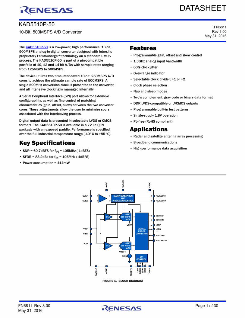
The KAD5510P-50 is a low-power, high performance, 10-bit, 500MSPS analog-to-digital converter designed with Intersil’s proprietary FemtoCharge™ technology on a standard CMOS process. The KAD5510P-50 is part of a pin-compatible portfolio of 10, 12 and 14-bit A/Ds with sample rates ranging from 125MSPS to 500MSPS.
The device utilizes two time-interleaved 10-bit, 250MSPS A/D cores to achieve the ultimate sample rate of 500MSPS. A single 500MHz conversion clock is presented to the converter, and all interleave clocking is managed internally.
A Serial Peripheral Interface (SPI) port allows for extensive configurability, as well as fine control of matching characteristics (gain, offset, skew) between the two converter cores. These adjustments allow the user to minimize spurs associated with the interleaving process.
Digital output data is presented in selectable LVDS or CMOS formats. The KAD5510P-50 is available in a 72 Ld QFN package with an exposed paddle. Performance is specified over the full industrial temperature range (-40°C to +85°C).
Key Specifications• SNR = 60.7dBFS for fIN = 105MHz (-1dBFS)
• SFDR = 83.2dBc for fIN = 105MHz (-1dBFS)
• Power consumption = 414mW
Features• Programmable gain, offset and skew control
• 1.3GHz analog input bandwidth
• 60fs clock jitter
• Over-range indicator
• Selectable clock divider: ÷1 or ÷2
• Clock phase selection
• Nap and sleep modes
• Two’s complement, gray code or binary data format
• DDR LVDS-compatible or LVCMOS outputs
• Programmable built-in test patterns
• Single-supply 1.8V operation
• Pb-free (RoHS compliant)
Applications• Radar and satellite antenna array processing
• Broadband communications
• High-performance data acquisition
DIGITALERROR
CORRECTION
SHA
1.25V
VINP
VINN
10-BIT250 MSPS
ADC
CLOCK GENERATIONAND
INTERLEAVE CONTROL
SHA10-BIT
250 MSPSADC
CLKP
CLKN
SPICONTROL
CSB
SCLK
SDIO
VREF
OG
ND
AGND
AVDD
CLKOUTP
CLKOUTN
D[9:0]P
D[9:0]N
ORP
ORN
OUTFMT
OUTMODE
OVD
D
CLKD
IV
NAPS
LP
SDO
+–
VCM
RESE
TN
VREF
FIGURE 1. BLOCK DIAGRAM
FN6811 Rev 3.00 Page 1 of 30May 31, 2016
KAD5510P-50
Table of ContentsOrdering Information . . . . . . . . . . . . . . . . . . . . . . . . . . . . . . . . . . . . . . . . . . . . . . . . . . . . . . . . . . . . . . . . . . . . . . . . . . . . . . . . . . . . . . . . 3
Pin-Compatible Family . . . . . . . . . . . . . . . . . . . . . . . . . . . . . . . . . . . . . . . . . . . . . . . . . . . . . . . . . . . . . . . . . . . . . . . . . . . . . . . . . . . . . . . 3
Absolute Maximum Ratings . . . . . . . . . . . . . . . . . . . . . . . . . . . . . . . . . . . . . . . . . . . . . . . . . . . . . . . . . . . . . . . . . . . . . . . . . . . . . . . . . . . 4
Thermal Information . . . . . . . . . . . . . . . . . . . . . . . . . . . . . . . . . . . . . . . . . . . . . . . . . . . . . . . . . . . . . . . . . . . . . . . . . . . . . . . . . . . . . . . . . 4
Electrical Specifications . . . . . . . . . . . . . . . . . . . . . . . . . . . . . . . . . . . . . . . . . . . . . . . . . . . . . . . . . . . . . . . . . . . . . . . . . . . . . . . . . . . . . 4
Digital Specifications . . . . . . . . . . . . . . . . . . . . . . . . . . . . . . . . . . . . . . . . . . . . . . . . . . . . . . . . . . . . . . . . . . . . . . . . . . . . . . . . . . . . . . . . 6
Timing Diagrams . . . . . . . . . . . . . . . . . . . . . . . . . . . . . . . . . . . . . . . . . . . . . . . . . . . . . . . . . . . . . . . . . . . . . . . . . . . . . . . . . . . . . . . . . . . . 6
Switching Specifications . . . . . . . . . . . . . . . . . . . . . . . . . . . . . . . . . . . . . . . . . . . . . . . . . . . . . . . . . . . . . . . . . . . . . . . . . . . . . . . . . . . . . 7
Pin Descriptions. . . . . . . . . . . . . . . . . . . . . . . . . . . . . . . . . . . . . . . . . . . . . . . . . . . . . . . . . . . . . . . . . . . . . . . . . . . . . . . . . . . . . . . . . . . . . 8
Pin Configuration. . . . . . . . . . . . . . . . . . . . . . . . . . . . . . . . . . . . . . . . . . . . . . . . . . . . . . . . . . . . . . . . . . . . . . . . . . . . . . . . . . . . . . . . . . . 10
Typical Performance Curves . . . . . . . . . . . . . . . . . . . . . . . . . . . . . . . . . . . . . . . . . . . . . . . . . . . . . . . . . . . . . . . . . . . . . . . . . . . . . . . . . 11
Theory of Operation. . . . . . . . . . . . . . . . . . . . . . . . . . . . . . . . . . . . . . . . . . . . . . . . . . . . . . . . . . . . . . . . . . . . . . . . . . . . . . . . . . . . . . . . . 14Functional Description . . . . . . . . . . . . . . . . . . . . . . . . . . . . . . . . . . . . . . . . . . . . . . . . . . . . . . . . . . . . . . . . . . . . . . . . . . . . . . . . . . . . . . . . . . . 14Power-On Calibration. . . . . . . . . . . . . . . . . . . . . . . . . . . . . . . . . . . . . . . . . . . . . . . . . . . . . . . . . . . . . . . . . . . . . . . . . . . . . . . . . . . . . . . . . . . . . 14User Initiated Reset . . . . . . . . . . . . . . . . . . . . . . . . . . . . . . . . . . . . . . . . . . . . . . . . . . . . . . . . . . . . . . . . . . . . . . . . . . . . . . . . . . . . . . . . . . . . . . 15Analog Input . . . . . . . . . . . . . . . . . . . . . . . . . . . . . . . . . . . . . . . . . . . . . . . . . . . . . . . . . . . . . . . . . . . . . . . . . . . . . . . . . . . . . . . . . . . . . . . . . . . . 15Clock Input . . . . . . . . . . . . . . . . . . . . . . . . . . . . . . . . . . . . . . . . . . . . . . . . . . . . . . . . . . . . . . . . . . . . . . . . . . . . . . . . . . . . . . . . . . . . . . . . . . . . . 16Jitter. . . . . . . . . . . . . . . . . . . . . . . . . . . . . . . . . . . . . . . . . . . . . . . . . . . . . . . . . . . . . . . . . . . . . . . . . . . . . . . . . . . . . . . . . . . . . . . . . . . . . . . . . . . 16Voltage Reference . . . . . . . . . . . . . . . . . . . . . . . . . . . . . . . . . . . . . . . . . . . . . . . . . . . . . . . . . . . . . . . . . . . . . . . . . . . . . . . . . . . . . . . . . . . . . . . 17Digital Outputs . . . . . . . . . . . . . . . . . . . . . . . . . . . . . . . . . . . . . . . . . . . . . . . . . . . . . . . . . . . . . . . . . . . . . . . . . . . . . . . . . . . . . . . . . . . . . . . . . . 17Over-Range Indicator. . . . . . . . . . . . . . . . . . . . . . . . . . . . . . . . . . . . . . . . . . . . . . . . . . . . . . . . . . . . . . . . . . . . . . . . . . . . . . . . . . . . . . . . . . . . . 17Power Dissipation . . . . . . . . . . . . . . . . . . . . . . . . . . . . . . . . . . . . . . . . . . . . . . . . . . . . . . . . . . . . . . . . . . . . . . . . . . . . . . . . . . . . . . . . . . . . . . . 17Nap/Sleep. . . . . . . . . . . . . . . . . . . . . . . . . . . . . . . . . . . . . . . . . . . . . . . . . . . . . . . . . . . . . . . . . . . . . . . . . . . . . . . . . . . . . . . . . . . . . . . . . . . . . . 17Data Format . . . . . . . . . . . . . . . . . . . . . . . . . . . . . . . . . . . . . . . . . . . . . . . . . . . . . . . . . . . . . . . . . . . . . . . . . . . . . . . . . . . . . . . . . . . . . . . . . . . . 18
Serial Peripheral Interface . . . . . . . . . . . . . . . . . . . . . . . . . . . . . . . . . . . . . . . . . . . . . . . . . . . . . . . . . . . . . . . . . . . . . . . . . . . . . . . . . . 20SPI Physical Interface . . . . . . . . . . . . . . . . . . . . . . . . . . . . . . . . . . . . . . . . . . . . . . . . . . . . . . . . . . . . . . . . . . . . . . . . . . . . . . . . . . . . . . . . . . . . 20SPI Configuration. . . . . . . . . . . . . . . . . . . . . . . . . . . . . . . . . . . . . . . . . . . . . . . . . . . . . . . . . . . . . . . . . . . . . . . . . . . . . . . . . . . . . . . . . . . . . . . . 21Device Information . . . . . . . . . . . . . . . . . . . . . . . . . . . . . . . . . . . . . . . . . . . . . . . . . . . . . . . . . . . . . . . . . . . . . . . . . . . . . . . . . . . . . . . . . . . . . . 21Indexed Device Configuration/Control . . . . . . . . . . . . . . . . . . . . . . . . . . . . . . . . . . . . . . . . . . . . . . . . . . . . . . . . . . . . . . . . . . . . . . . . . . . . . . 21Global Device Configuration/Control . . . . . . . . . . . . . . . . . . . . . . . . . . . . . . . . . . . . . . . . . . . . . . . . . . . . . . . . . . . . . . . . . . . . . . . . . . . . . . . 22Device Test . . . . . . . . . . . . . . . . . . . . . . . . . . . . . . . . . . . . . . . . . . . . . . . . . . . . . . . . . . . . . . . . . . . . . . . . . . . . . . . . . . . . . . . . . . . . . . . . . . . . . 23
Equivalent Circuits . . . . . . . . . . . . . . . . . . . . . . . . . . . . . . . . . . . . . . . . . . . . . . . . . . . . . . . . . . . . . . . . . . . . . . . . . . . . . . . . . . . . . . . . . 25
ADC Evaluation Platform . . . . . . . . . . . . . . . . . . . . . . . . . . . . . . . . . . . . . . . . . . . . . . . . . . . . . . . . . . . . . . . . . . . . . . . . . . . . . . . . . . . . 26
Layout Considerations . . . . . . . . . . . . . . . . . . . . . . . . . . . . . . . . . . . . . . . . . . . . . . . . . . . . . . . . . . . . . . . . . . . . . . . . . . . . . . . . . . . . . . 26Split Ground and Power Planes . . . . . . . . . . . . . . . . . . . . . . . . . . . . . . . . . . . . . . . . . . . . . . . . . . . . . . . . . . . . . . . . . . . . . . . . . . . . . . . . . . . . 26Clock Input Considerations. . . . . . . . . . . . . . . . . . . . . . . . . . . . . . . . . . . . . . . . . . . . . . . . . . . . . . . . . . . . . . . . . . . . . . . . . . . . . . . . . . . . . . . . 26Exposed Paddle . . . . . . . . . . . . . . . . . . . . . . . . . . . . . . . . . . . . . . . . . . . . . . . . . . . . . . . . . . . . . . . . . . . . . . . . . . . . . . . . . . . . . . . . . . . . . . . . . 26Bypass and Filtering . . . . . . . . . . . . . . . . . . . . . . . . . . . . . . . . . . . . . . . . . . . . . . . . . . . . . . . . . . . . . . . . . . . . . . . . . . . . . . . . . . . . . . . . . . . . . 26LVDS Outputs . . . . . . . . . . . . . . . . . . . . . . . . . . . . . . . . . . . . . . . . . . . . . . . . . . . . . . . . . . . . . . . . . . . . . . . . . . . . . . . . . . . . . . . . . . . . . . . . . . . 26LVCMOS Outputs . . . . . . . . . . . . . . . . . . . . . . . . . . . . . . . . . . . . . . . . . . . . . . . . . . . . . . . . . . . . . . . . . . . . . . . . . . . . . . . . . . . . . . . . . . . . . . . . 26Unused Inputs . . . . . . . . . . . . . . . . . . . . . . . . . . . . . . . . . . . . . . . . . . . . . . . . . . . . . . . . . . . . . . . . . . . . . . . . . . . . . . . . . . . . . . . . . . . . . . . . . . 27Definitions . . . . . . . . . . . . . . . . . . . . . . . . . . . . . . . . . . . . . . . . . . . . . . . . . . . . . . . . . . . . . . . . . . . . . . . . . . . . . . . . . . . . . . . . . . . . . . . . . . . . . 27
Revision History. . . . . . . . . . . . . . . . . . . . . . . . . . . . . . . . . . . . . . . . . . . . . . . . . . . . . . . . . . . . . . . . . . . . . . . . . . . . . . . . . . . . . . . . . . . . 28
About Intersil . . . . . . . . . . . . . . . . . . . . . . . . . . . . . . . . . . . . . . . . . . . . . . . . . . . . . . . . . . . . . . . . . . . . . . . . . . . . . . . . . . . . . . . . . . . . . . 29
Package Outline Drawing . . . . . . . . . . . . . . . . . . . . . . . . . . . . . . . . . . . . . . . . . . . . . . . . . . . . . . . . . . . . . . . . . . . . . . . . . . . . . . . . . . . . 30
FN6811 Rev 3.00 Page 2 of 30May 31, 2016

KAD5510P-50
Ordering InformationPART NUMBER
(Notes 1, 2) PART MARKINGSPEED(MSPS)
TEMP. RANGE(°C)
PACKAGE(RoHS Compliant)
PKG.DWG. #
KAD5510P-50Q72 KAD5510P-50 Q72EP-I 500 -40 to +85 72 Ld QFN L72.10x10D
NOTES:
1. These Intersil Pb-free plastic packaged products employ special Pb-free material sets; molding compounds/die attach materials and NiPdAu plate - e4 termination finish, which is RoHS compliant and compatible with both SnPb and Pb-free soldering operations. Intersil Pb-free products are MSL classified at Pb-free peak reflow temperatures that meet or exceed the Pb-free requirements of IPC/JEDEC J STD-020.
2. For Moisture Sensitivity Level (MSL), please see product information page for KAD5510P-50. For more information on MSL, please see tech brief TB363.
Pin-Compatible Family
MODEL RESOLUTIONSPEED(MSPS)
KAD5514P-25 14 250
KAD5514P-21 14 210
KAD5514P-17 14 170
KAD5514P-12 14 125
KAD5512P-50 12 500
KAD5512P-25, KAD5512HP-25 12 250
KAD5512P-21, KAD5512HP-21 12 210
KAD5512P-17, KAD5512HP-17 12 170
KAD5512P-12, KAD5512HP-12 12 125
KAD5510P-50 10 500
FN6811 Rev 3.00 Page 3 of 30May 31, 2016
KAD5510P-50
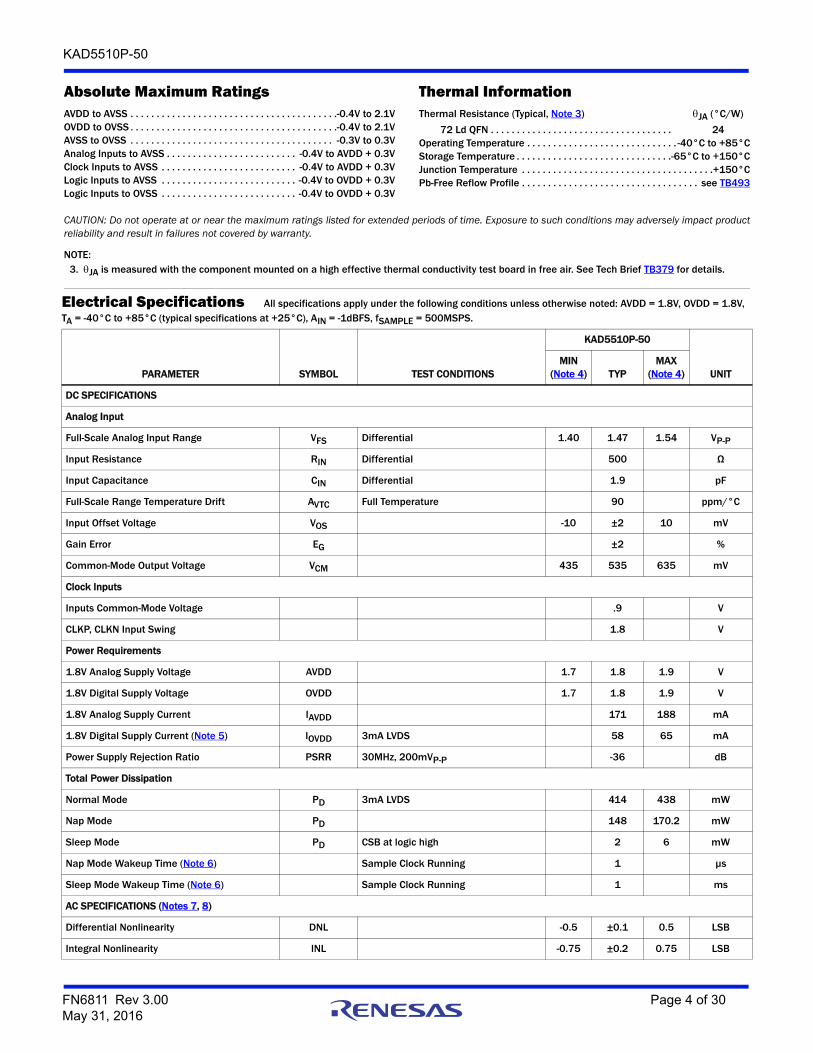
Absolute Maximum Ratings Thermal InformationAVDD to AVSS . . . . . . . . . . . . . . . . . . . . . . . . . . . . . . . . . . . . . . . .-0.4V to 2.1VOVDD to OVSS . . . . . . . . . . . . . . . . . . . . . . . . . . . . . . . . . . . . . . . .-0.4V to 2.1VAVSS to OVSS . . . . . . . . . . . . . . . . . . . . . . . . . . . . . . . . . . . . . . . -0.3V to 0.3VAnalog Inputs to AVSS . . . . . . . . . . . . . . . . . . . . . . . . . -0.4V to AVDD + 0.3VClock Inputs to AVSS . . . . . . . . . . . . . . . . . . . . . . . . . . -0.4V to AVDD + 0.3VLogic Inputs to AVSS . . . . . . . . . . . . . . . . . . . . . . . . . . -0.4V to OVDD + 0.3VLogic Inputs to OVSS . . . . . . . . . . . . . . . . . . . . . . . . . . -0.4V to OVDD + 0.3V
Thermal Resistance (Typical, Note 3) JA (°C/W)
72 Ld QFN . . . . . . . . . . . . . . . . . . . . . . . . . . . . . . . . . . . 24Operating Temperature . . . . . . . . . . . . . . . . . . . . . . . . . . . . . -40°C to +85°CStorage Temperature . . . . . . . . . . . . . . . . . . . . . . . . . . . . . .-65°C to +150°CJunction Temperature . . . . . . . . . . . . . . . . . . . . . . . . . . . . . . . . . . . . .+150°CPb-Free Reflow Profile . . . . . . . . . . . . . . . . . . . . . . . . . . . . . . . . . . see TB493
CAUTION: Do not operate at or near the maximum ratings listed for extended periods of time. Exposure to such conditions may adversely impact productreliability and result in failures not covered by warranty.
NOTE:3. JA is measured with the component mounted on a high effective thermal conductivity test board in free air. See Tech Brief TB379 for details.
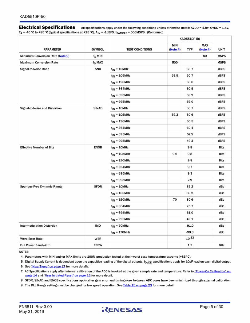
Electrical Specifications All specifications apply under the following conditions unless otherwise noted: AVDD = 1.8V, OVDD = 1.8V, TA = -40°C to +85°C (typical specifications at +25°C), AIN = -1dBFS, fSAMPLE = 500MSPS.
PARAMETER SYMBOL TEST CONDITIONS
KAD5510P-50
UNITMIN
(Note 4) TYPMAX
(Note 4)
DC SPECIFICATIONS
Analog Input
Full-Scale Analog Input Range VFS Differential 1.40 1.47 1.54 VP-P
Input Resistance RIN Differential 500 Ω
Input Capacitance CIN Differential 1.9 pF
Full-Scale Range Temperature Drift AVTC Full Temperature 90 ppm/°C
Input Offset Voltage VOS -10 ±2 10 mV
Gain Error EG ±2 %
Common-Mode Output Voltage VCM 435 535 635 mV
Clock Inputs
Inputs Common-Mode Voltage .9 V
CLKP, CLKN Input Swing 1.8 V
Power Requirements
1.8V Analog Supply Voltage AVDD 1.7 1.8 1.9 V
1.8V Digital Supply Voltage OVDD 1.7 1.8 1.9 V
1.8V Analog Supply Current IAVDD 171 188 mA
1.8V Digital Supply Current (Note 5) IOVDD 3mA LVDS 58 65 mA
Power Supply Rejection Ratio PSRR 30MHz, 200mVP-P -36 dB
Total Power Dissipation
Normal Mode PD 3mA LVDS 414 438 mW
Nap Mode PD 148 170.2 mW
Sleep Mode PD CSB at logic high 2 6 mW
Nap Mode Wakeup Time (Note 6) Sample Clock Running 1 µs
Sleep Mode Wakeup Time (Note 6) Sample Clock Running 1 ms
AC SPECIFICATIONS (Notes 7, 8)
Differential Nonlinearity DNL -0.5 ±0.1 0.5 LSB
Integral Nonlinearity INL -0.75 ±0.2 0.75 LSB
FN6811 Rev 3.00 Page 4 of 30May 31, 2016
KAD5510P-50
Minimum Conversion Rate (Note 9) fS MIN 80 MSPS
Maximum Conversion Rate fS MAX 500 MSPS
Signal-to-Noise Ratio SNR fIN = 10MHz 60.7 dBFS
fIN = 105MHz 59.5 60.7 dBFS
fIN = 190MHz 60.6 dBFS
fIN = 364MHz 60.5 dBFS
fIN = 695MHz 59.9 dBFS
fIN = 995MHz 59.0 dBFS
Signal-to-Noise and Distortion SINAD fIN = 10MHz 60.7 dBFS
fIN = 105MHz 59.3 60.6 dBFS
fIN = 190MHz 60.5 dBFS
fIN = 364MHz 60.4 dBFS
fIN = 695MHz 57.5 dBFS
fIN = 995MHz 49.3 dBFS
Effective Number of Bits ENOB fIN = 10MHz 9.8 Bits
fIN = 105MHz 9.6 9.8 Bits
fIN = 190MHz 9.8 Bits
fIN = 364MHz 9.7 Bits
fIN = 695MHz 9.3 Bits
fIN = 995MHz 7.9 Bits
Spurious-Free Dynamic Range SFDR fIN = 10MHz 83.2 dBc
fIN = 105MHz 83.2 dBc
fIN = 190MHz 70 80.6 dBc
fIN = 364MHz 75.7 dBc
fIN = 695MHz 61.0 dBc
fIN = 995MHz 49.1 dBc
Intermodulation Distortion IMD fIN = 70MHz -91.0 dBc
fIN = 170MHz -90.3 dBc
Word Error Rate WER 10-12
Full Power Bandwidth FPBW 1.3 GHz
NOTES:
4. Parameters with MIN and/or MAX limits are 100% production tested at their worst case temperature extreme (+85°C).
5. Digital Supply Current is dependent upon the capacitive loading of the digital outputs. IOVDD specifications apply for 10pF load on each digital output.
6. See “Nap/Sleep” on page 17 for more details.
7. AC Specifications apply after internal calibration of the ADC is invoked at the given sample rate and temperature. Refer to “Power-On Calibration” on page 14 and “User Initiated Reset” on page 15 for more detail.
8. SFDR, SINAD and ENOB specifications apply after gain error and timing skew between ADC cores have been minimized through external calibration.
9. The DLL Range setting must be changed for low speed operation. See Table 15 on page 23 for more detail.
Electrical Specifications All specifications apply under the following conditions unless otherwise noted: AVDD = 1.8V, OVDD = 1.8V, TA = -40°C to +85°C (typical specifications at +25°C), AIN = -1dBFS, fSAMPLE = 500MSPS. (Continued)
PARAMETER SYMBOL TEST CONDITIONS
KAD5510P-50
UNITMIN
(Note 4) TYPMAX
(Note 4)
FN6811 Rev 3.00 Page 5 of 30May 31, 2016

KAD5510P-50
Digital SpecificationsPARAMETER SYMBOL TEST CONDITIONS MIN TYP MAX UNIT
INPUTS
Input Current High (SDIO, RESETN) IIH VIN = 1.8V 0 1 10 µA
Input Current Low (SDIO, RESETN) IIL VIN = 0V -25 -12 -5 µA
Input Voltage High (SDIO, RESETN) VIH 1.17 V
Input Voltage Low (SDIO, RESETN) VIL .63 V
Input Current High (OUTMODE, NAPSLP, CLKDIV, OUTFMT) (Note 10)
IIH 15 25 40 µA
Input Current Low (OUTMODE, NAPSLP, CLKDIV, OUTFMT)
IIL -40 25 -15 µA
Input Capacitance CDI 3 pF
LVDS OUTPUTS
Differential Output Voltage VT 620 mVP-P
Output Offset Voltage VOS 950 965 980 mV
Output Rise Time tR 500 ps
Output Fall Time tF 500 ps
CMOS OUTPUTS
Voltage Output High VOH IOH = -500µA OVDD - 0.3 OVDD - 0.1 V
Voltage Output Low VOL IOL = 1mA 0.1 0.3 V
Output Rise Time tR 1.8 ns
Output Fall Time tF 1.4 ns
Timing Diagrams
FIGURE 2. LVDS TIMING DIAGRAM (See “Digital Outputs” on page 17)
FIGURE 3. CMOS TIMING DIAGRAM (See “Digital Outputs” on page 17)
INP
INN
CLKPCLKN
CLKOUTPCLKOUTN
D[9:0]ND[9:0]P
tA
tCPD
tDC
tPD
DATAN-L
LATENCY = L CYCLES
SAMPLE N
DATAN
DATAN-L+1
DATAN-L+2
INP
INN
CLKPCLKN
tA
tCPD
tDC
tPD
LATENCY = L CYCLES
SAMPLE N
CLKOUTPCLKOUTN
D[9:0]ND[9:0]P
DATAN-L
DATAN
DATAN-L+1 DATA
N-L+2
FN6811 Rev 3.00 Page 6 of 30May 31, 2016

KAD5510P-50
Switching SpecificationsPARAMETER TEST CONDITIONS SYMBOL MIN TYP MAX UNIT
ADC OUTPUT
Aperture Delay tA 375 ps
RMS Aperture Jitter jA 60 fs
Output Clock to Data Propagation Delay, LVDS Mode (Note 11)
Rising Edge tDC -260 -50 120 ps
Falling Edge tDC -160 10 230 ps
Output Clock to Data Propagation Delay, CMOS Mode (Note 11)
Rising Edge tDC -220 -10 200 ps
Falling Edge tDC -310 -90 110 ps
Latency (Pipeline Delay) L 15 cycles
Overvoltage Recovery tOVR 1 cycles
SPI INTERFACE (Notes 12, 13)
SCLK Period Write Operation tCLK 32 cycles(Note 12)
Read Operation tCLK 132 cycles
SCLK Duty Cycle (tHI/tCLK or tLO/tCLK) Read or Write 25 50 75 %
CSBto SCLK Set-up Time Read or Write tS 2 cycles
CSBafter SCLK Hold Time Read or Write tH 6 cycles
Data Valid to SCLK Set-up Time Write tDSW 2 cycles
Data Valid after SCLK Hold Time Write tDHW 6 cycles
Data Valid after SCLK Time Read tDVR 33 cycles
Data Invalid after SCLK Time Read tDHR 6 cycles
Sleep Mode CSBto SCLK Set-up Time (Note 14)
Read or Write in Sleep Mode tS 150 µs
NOTES:
10. The Tri-Level Inputs internal switching thresholds are approximately 0.43V and 1.34V. It is advised to float the inputs, tie to ground or AVDD depending on desired function.
11. The input clock to output clock delay is a function of sample rate, using the output clock to latch the data simplifies data capture for most applications. Contact support for more info if needed.
12. SPI Interface timing is directly proportional to the ADC sample period (tS). (2ns at 500Msps).
13. The SPI may operate asynchronously with respect to the ADC sample clock.
14. The CSB set-up time increases in sleep mode due to the reduced power state, CSB set-up time in Nap mode is equal to normal mode CSB set-up time (4ns min).
FN6811 Rev 3.00 Page 7 of 30May 31, 2016
KAD5510P-50
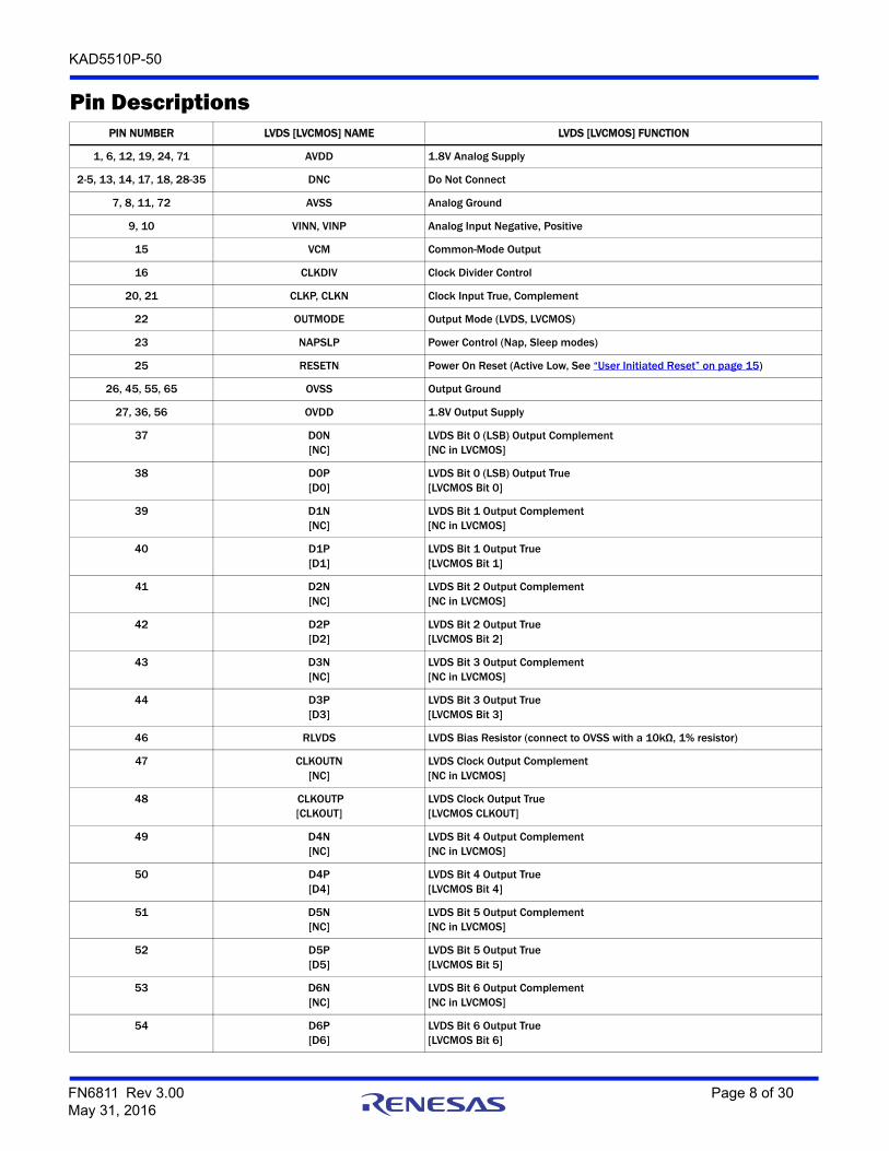
Pin DescriptionsPIN NUMBER LVDS [LVCMOS] NAME LVDS [LVCMOS] FUNCTION
1, 6, 12, 19, 24, 71 AVDD 1.8V Analog Supply
2-5, 13, 14, 17, 18, 28-35 DNC Do Not Connect
7, 8, 11, 72 AVSS Analog Ground
9, 10 VINN, VINP Analog Input Negative, Positive
15 VCM Common-Mode Output
16 CLKDIV Clock Divider Control
20, 21 CLKP, CLKN Clock Input True, Complement
22 OUTMODE Output Mode (LVDS, LVCMOS)
23 NAPSLP Power Control (Nap, Sleep modes)
25 RESETN Power On Reset (Active Low, See “User Initiated Reset” on page 15)
26, 45, 55, 65 OVSS Output Ground
27, 36, 56 OVDD 1.8V Output Supply
37 D0N[NC]
LVDS Bit 0 (LSB) Output Complement [NC in LVCMOS]
38 D0P [D0]
LVDS Bit 0 (LSB) Output True [LVCMOS Bit 0]
39 D1N[NC]
LVDS Bit 1 Output Complement [NC in LVCMOS]
40 D1P [D1]
LVDS Bit 1 Output True [LVCMOS Bit 1]
41 D2N[NC]
LVDS Bit 2 Output Complement [NC in LVCMOS]
42 D2P [D2]
LVDS Bit 2 Output True [LVCMOS Bit 2]
43 D3N[NC]
LVDS Bit 3 Output Complement [NC in LVCMOS]
44 D3P [D3]
LVDS Bit 3 Output True [LVCMOS Bit 3]
46 RLVDS LVDS Bias Resistor (connect to OVSS with a 10kΩ, 1% resistor)
47 CLKOUTN[NC]
LVDS Clock Output Complement[NC in LVCMOS]
48 CLKOUTP[CLKOUT]
LVDS Clock Output True[LVCMOS CLKOUT]
49 D4N[NC]
LVDS Bit 4 Output Complement [NC in LVCMOS]
50 D4P [D4]
LVDS Bit 4 Output True [LVCMOS Bit 4]
51 D5N[NC]
LVDS Bit 5 Output Complement [NC in LVCMOS]
52 D5P [D5]
LVDS Bit 5 Output True [LVCMOS Bit 5]
53 D6N[NC]
LVDS Bit 6 Output Complement [NC in LVCMOS]
54 D6P [D6]
LVDS Bit 6 Output True [LVCMOS Bit 6]
FN6811 Rev 3.00 Page 8 of 30May 31, 2016
KAD5510P-50
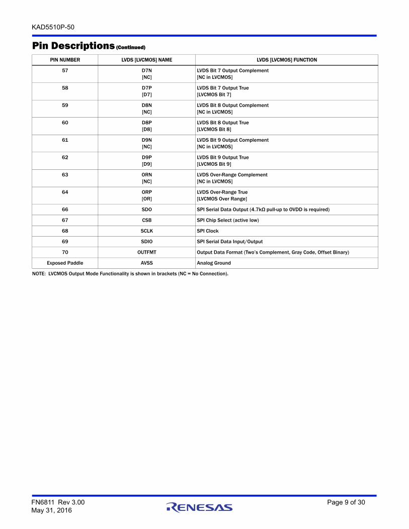
57 D7N[NC]
LVDS Bit 7 Output Complement [NC in LVCMOS]
58 D7P [D7]
LVDS Bit 7 Output True [LVCMOS Bit 7]
59 D8N[NC]
LVDS Bit 8 Output Complement [NC in LVCMOS]
60 D8P [D8]
LVDS Bit 8 Output True [LVCMOS Bit 8]
61 D9N[NC]
LVDS Bit 9 Output Complement [NC in LVCMOS]
62 D9P [D9]
LVDS Bit 9 Output True [LVCMOS Bit 9]
63 ORN[NC]
LVDS Over-Range Complement[NC in LVCMOS]
64 ORP[OR]
LVDS Over-Range True[LVCMOS Over Range]
66 SDO SPI Serial Data Output (4.7kΩ pull-up to OVDD is required)
67 CSB SPI Chip Select (active low)
68 SCLK SPI Clock
69 SDIO SPI Serial Data Input/Output
70 OUTFMT Output Data Format (Two’s Complement, Gray Code, Offset Binary)
Exposed Paddle AVSS Analog Ground
NOTE: LVCMOS Output Mode Functionality is shown in brackets (NC = No Connection).
Pin Descriptions (Continued)
PIN NUMBER LVDS [LVCMOS] NAME LVDS [LVCMOS] FUNCTION
FN6811 Rev 3.00 Page 9 of 30May 31, 2016
KAD5510P-50
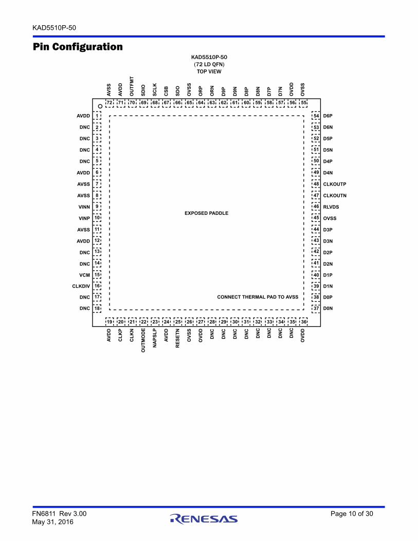
Pin ConfigurationKAD5510P-50(72 LD QFN)
TOP VIEW
AV
SS
AV
DD
OU
TF
MT
SD
IO
72 71 70 69 68 67 66 65 64 63 62 61
SC
LK
CS
B
SD
O
OV
SS
OR
P
OR
N
D9
P
D9
N
60 59
D8
P
D8
N
D6P
D6N
D5P
D5N
D4P
D4N
CLKOUTP
CLKOUTN
RLVDS
OVSS
D3P
D3N
D2P
D2N
1
2
3
4
5
6
7
8
9
10
11
12
13
14
54
53
52
51
50
49
48
47
46
45
44
43
42
41
AVDD
DNC
DNC
DNC
DNC
AVDD
AVSS
AVSS
VINN
VINP
AVSS
AVDD
DNC
DNC
19 20 21 22 23 24 25 26 27 28 29 30 31 32
AV
DD
CL
KP
CL
KN
OU
TM
OD
E
NA
PS
LP
AV
DD
RE
SE
TN
OV
SS
OV
DD
DN
C
DN
C
DN
C
DN
C
DN
C
15
16
17
18
VCM
CLKDIV
DNC
DNC
33 34 35 36
DN
C
DN
C
DN
C
OV
DD
D1P
D1N
D0P
D0N
40
39
38
37
58 57
D7
P
D7
N
56 55
OV
DD
OV
SS
CONNECT THERMAL PAD TO AVSS
EXPOSED PADDLE
FN6811 Rev 3.00 Page 10 of 30May 31, 2016
KAD5510P-50
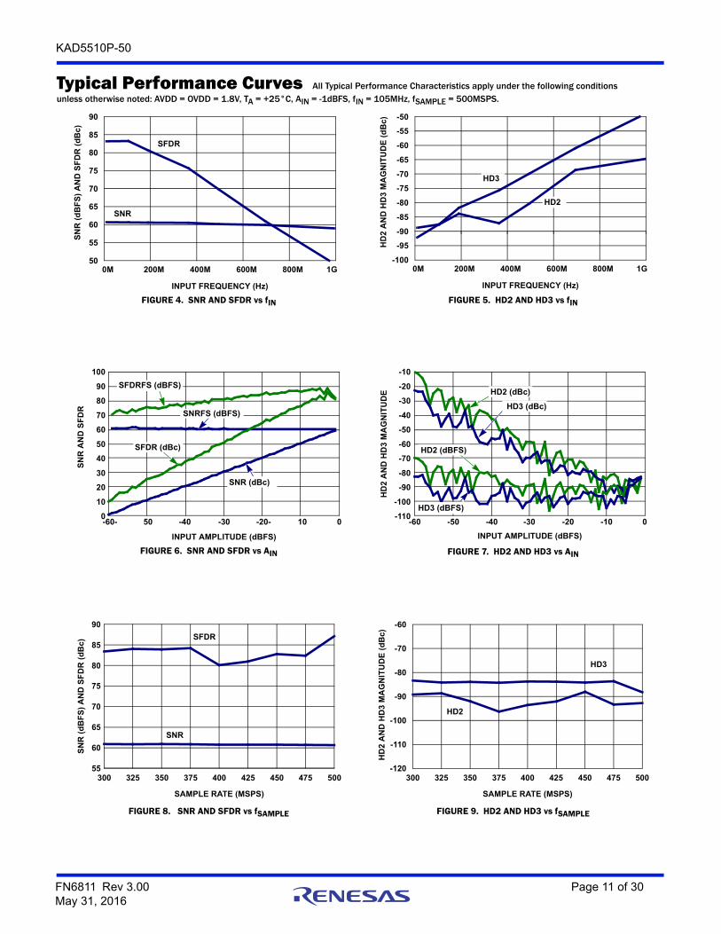
Typical Performance Curves All Typical Performance Characteristics apply under the following conditions unless otherwise noted: AVDD = OVDD = 1.8V, TA = +25°C, AIN = -1dBFS, fIN = 105MHz, fSAMPLE = 500MSPS.
FIGURE 4. SNR AND SFDR vs fIN FIGURE 5. HD2 AND HD3 vs fIN
FIGURE 6. SNR AND SFDR vs AIN FIGURE 7. HD2 AND HD3 vs AIN
FIGURE 8. SNR AND SFDR vs fSAMPLE FIGURE 9. HD2 AND HD3 vs fSAMPLE
50
55
60
65
70
75
80
85
90
0M 200M 400M 600M 800M 1G
INPUT FREQUENCY (Hz)
SN
R (
dB
FS
) A
ND
SF
DR
(d
Bc
)
SNR
SFDR
-100
-95
-90
-85
-80
-75
-70
-65
-60
-55
-50
0M 200M 400M 600M 800M 1G
INPUT FREQUENCY (Hz)
HD
2 A
ND
HD
3 M
AG
NIT
UD
E (
dB
c)
HD3
HD2
0
10
20
30
40
50
60
70
80
90
100
-60- 50 -40 -30 -20- 10 0
INPUT AMPLITUDE (dBFS)
SN
R A
ND
SF
DR
SNR (dBc)
SFDR (dBc)
SNRFS (dBFS)
SFDRFS (dBFS)
-110
-100
-90
-80
-70
-60
-50
-40
-30
-20
-10
-60 -50 -40 -30 -20 -10 0
INPUT AMPLITUDE (dBFS)
HD
2 A
ND
HD
3 M
AG
NIT
UD
E
HD2 (dBFS)
HD3 (dBFS)
HD3 (dBc)
HD2 (dBc)
SFDR
55
60
65
70
75
80
85
90
300 325 350 375 400 425 450 475 500
SAMPLE RATE (MSPS)
SN
R (
dB
FS
) A
ND
SF
DR
(d
Bc
)
SNR
-120
-110
-100
-90
-80
-70
-60
300 325 350 375 400 425 450 475 500
SAMPLE RATE (MSPS)
HD
2 A
ND
HD
3 M
AG
NIT
UD
E (
dB
c)
HD2
HD3
FN6811 Rev 3.00 Page 11 of 30May 31, 2016

KAD5510P-50
FIGURE 10. POWER vs fSAMPLE IN 3mA LVDS MODE FIGURE 11. DIFFERENTIAL NONLINEARITY
FIGURE 12. INTEGRAL NONLINEARITY FIGURE 13. SNR AND SFDR vs VCM
FIGURE 14. NOISE HISTOGRAM FIGURE 15. SINGLE-TONE SPECTRUM AT 105MHz
Typical Performance Curves All Typical Performance Characteristics apply under the following conditions unless otherwise noted: AVDD = OVDD = 1.8V, TA = +25°C, AIN = -1dBFS, fIN = 105MHz, fSAMPLE = 500MSPS. (Continued)
0
50
100
150
200
250
300
350
400
450
80 140 200 260 320 380 440 500
SAMPLE RATE (MSPS)
TO
TAL
PO
WE
R (
mW
)
-0.25
-0.20
-0.15
-0.10
-0.05
0.00
0.05
0.10
0.15
0.20
0.25
0 128 256 384 512 640 768 896 1024
CODE
DN
L (
LS
Bs
)
-0.25
-0.20
-0.15
-0.10
-0.05
0.00
0.05
0.10
0.15
0.20
0.25
0 128 256 384 512 640 768 896 1024
CODE
INL
(L
SB
s)
50
55
60
65
70
75
80
85
90
300 400 500 600 700 800
INPUT COMMON MODE (mV)
SN
R (
dB
FS
) A
ND
SF
DR
(d
Bc)
SNR
SFDR
508 509 510 511 512 513 514 515 516 5170
100000
200000
300000
400000
500000
600000
700000
800000
900000
1000000
CODE
NU
MB
ER
OF
HIT
S
0M 50M 100M 150M 200M 250M-120
-100
-80
-60
-40
-20
0
FREQUENCY (Hz)
AIN = -1.0dBFS SNR = 60.7dBFS SFDR = 82.4dBc SINAD = 60.6dBFS
AM
PL
ITU
DE
(d
BF
S)
FN6811 Rev 3.00 Page 12 of 30May 31, 2016

KAD5510P-50
FIGURE 16. SINGLE-TONE SPECTRUM AT 190MHz FIGURE 17. SINGLE-TONE SPECTRUM AT 495MHz
FIGURE 18. SINGLE-TONE SPECTRUM AT 995MHz FIGURE 19. TWO-TONE SPECTRUM AT 70MHz
FIGURE 20. TWO-TONE SPECTRUM AT 170MHz
Typical Performance Curves All Typical Performance Characteristics apply under the following conditions unless otherwise noted: AVDD = OVDD = 1.8V, TA = +25°C, AIN = -1dBFS, fIN = 105MHz, fSAMPLE = 500MSPS. (Continued)
0M 50M 100M 150M 200M 250M-120
-100
-80
-60
-40
-20
0
FREQUENCY (Hz)
AIN = -1.0dBFS SNR = 60.5dBFS SFDR = 77.7dBc SINAD = 60.4dBFS
AM
PL
ITU
DE
(d
BF
S)
0M 50M 100M 150M 200M 250M
FREQUENCY (Hz)
AIN = -1.0dBFS SNR = 60.2dBFS SFDR = 69.4dBc SINAD = 59.8dBFS
-120
-100
-80
-60
-40
-20
0
AM
PL
ITU
DE
(d
BF
S)
0M 50M 100M 150M 200M 250M-120
-100
-80
-60
-40
-20
0AIN = -1.0dBFS SNR = 58.7dBFS SFDR = 49.6dBc SINAD = 49.7dBFS
AM
PL
ITU
DE
(d
BF
S)
FREQUENCY (Hz)
0M 50M 100M 150M 200M 250M-120
-100
-80
-60
-40
-20
0
IMD = -91.0dBFS
FREQUENCY (Hz)
AM
PL
ITU
DE
(d
BF
S)
0M 50M 100M 150M 200M 250M-120
-100
-80
-60
-40
-20
0
IMD = -90.3dBFS
FREQUENCY (Hz)
AM
PL
ITU
DE
(d
BF
S)
FN6811 Rev 3.00 Page 13 of 30May 31, 2016
KAD5510P-50
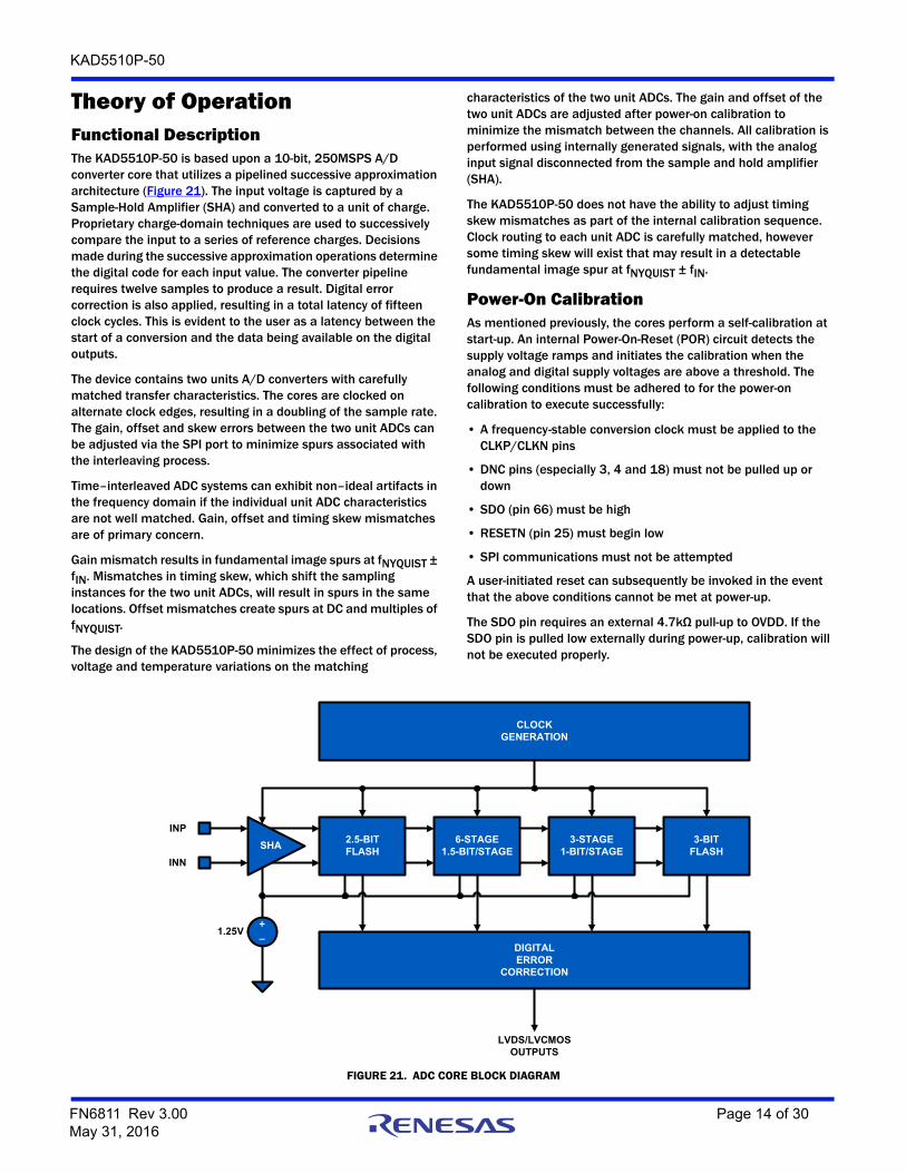
Theory of OperationFunctional DescriptionThe KAD5510P-50 is based upon a 10-bit, 250MSPS A/D converter core that utilizes a pipelined successive approximation architecture (Figure 21). The input voltage is captured by a Sample-Hold Amplifier (SHA) and converted to a unit of charge. Proprietary charge-domain techniques are used to successively compare the input to a series of reference charges. Decisions made during the successive approximation operations determine the digital code for each input value. The converter pipeline requires twelve samples to produce a result. Digital error correction is also applied, resulting in a total latency of fifteen clock cycles. This is evident to the user as a latency between the start of a conversion and the data being available on the digital outputs.
The device contains two units A/D converters with carefully matched transfer characteristics. The cores are clocked on alternate clock edges, resulting in a doubling of the sample rate. The gain, offset and skew errors between the two unit ADCs can be adjusted via the SPI port to minimize spurs associated with the interleaving process.
Time–interleaved ADC systems can exhibit non–ideal artifacts in the frequency domain if the individual unit ADC characteristics are not well matched. Gain, offset and timing skew mismatches are of primary concern.
Gain mismatch results in fundamental image spurs at fNYQUIST ± fIN. Mismatches in timing skew, which shift the sampling instances for the two unit ADCs, will result in spurs in the same locations. Offset mismatches create spurs at DC and multiples of fNYQUIST.
The design of the KAD5510P-50 minimizes the effect of process, voltage and temperature variations on the matching
characteristics of the two unit ADCs. The gain and offset of the two unit ADCs are adjusted after power-on calibration to minimize the mismatch between the channels. All calibration is performed using internally generated signals, with the analog input signal disconnected from the sample and hold amplifier (SHA).
The KAD5510P-50 does not have the ability to adjust timing skew mismatches as part of the internal calibration sequence. Clock routing to each unit ADC is carefully matched, however some timing skew will exist that may result in a detectable fundamental image spur at fNYQUIST ± fIN.
Power-On CalibrationAs mentioned previously, the cores perform a self-calibration at start-up. An internal Power-On-Reset (POR) circuit detects the supply voltage ramps and initiates the calibration when the analog and digital supply voltages are above a threshold. The following conditions must be adhered to for the power-on calibration to execute successfully:
• A frequency-stable conversion clock must be applied to the CLKP/CLKN pins
• DNC pins (especially 3, 4 and 18) must not be pulled up or down
• SDO (pin 66) must be high
• RESETN (pin 25) must begin low
• SPI communications must not be attempted
A user-initiated reset can subsequently be invoked in the event that the above conditions cannot be met at power-up.
The SDO pin requires an external 4.7kΩ pull-up to OVDD. If the SDO pin is pulled low externally during power-up, calibration will not be executed properly.
FIGURE 21. ADC CORE BLOCK DIAGRAM
DIGITALERROR
CORRECTION
SHA
1.25V
INP
INN
CLOCKGENERATION
2.5-BITFLASH
6-STAGE1.5-BIT/STAGE
3-STAGE1-BIT/STAGE
3-BITFLASH
LVDS/LVCMOSOUTPUTS
+
–
FN6811 Rev 3.00 Page 14 of 30May 31, 2016

KAD5510P-50
After the power supply has stabilized the internal POR releases RESETN and an internal pull-up pulls it high, which starts the calibration sequence. If a subsequent user-initiated reset is required, the RESETN pin should be connected to an open-drain driver with a drive strength of less than 0.5mA.
The calibration sequence is initiated on the rising edge of RESETN, as shown in Figure 22. The Over-Range (OR) output is set high once RESETN is pulled low, and remains in that state until calibration is complete. The OR output returns to normal operation at that time, so it is important that the analog input be within the converter’s full-scale range to observe the transition. If the input is in an over-range condition the OR pin will stay high, and it will not be possible to detect the end of the calibration cycle.
While RESETN is low, the output clock (CLKOUTP/CLKOUTN) is set low. Normal operation of the output clock resumes at the next input clock edge (CLKP/CLKN) after RESETN is deasserted. At 500MSPS the nominal calibration time is 200ms, while the maximum calibration time is 550ms.
User Initiated ResetRecalibration of the ADC can be initiated at any time by driving the RESETN pin low for a minimum of one clock cycle. An open-drain driver with a drive strength of less than 0.5mA is recommended, RESETN has an internal high impedance pull-up to OVDD. As is the case during power-on reset, the SDO, RESETN and DNC pins must be in the proper state for the calibration to successfully execute.
The performance of the KAD5510P-50 changes with variations in temperature, supply voltage or sample rate. The extent of these changes may necessitate recalibration, depending on system performance requirements. Best performance will be achieved by recalibrating the ADC under the environmental conditions at which it will operate.
A supply voltage variation of less than 100mV will generally result in an SNR change of less than 0.1dBFS and SFDR change of less than 3dBc.
In situations where the sample rate is not constant, best results will be obtained if the device is calibrated at the highest sample rate. Reducing the sample rate by less than 80MSPS will typically result in an SNR change of less than 0.1dBFS and an SFDR change of less than 3dBc.
Figures 23 and 24 show the effect of temperature on SNR and SFDR performance with calibration performed at -40°C, +25°C, and +85°C. Each plot shows the variation of SNR/SFDR across temperature after a single calibration at -40°C, +25°C and +85°C. Best performance is typically achieved by calibration at the operating conditions as stated earlier but it can be seen that performance drift with temperature is not a very strong function of the temperature at which the calibration is performed.
Analog InputA single fully differential input (VINP/VINN) connects to the sample and hold amplifier (SHA) of each unit ADC. The ideal full-scale input voltage is 1.45V, centered at the VCM voltage of 0.535V as shown in Figure 25.
FIGURE 22. CALIBRATION TIMING
CLKPCLKN
CLKOUTP
RESETN
ORP
CALIBRATION BEGINS
CALIBRATION COMPLETE
CALIBRATION TIME
FIGURE 23. SNR PERFORMANCE vs TEMPERATURE
-4
-3
-2
-1
0
1
2
3
-40 -15 10 35 60 85
SN
R C
HA
NG
E (
dB
fs) CAL DONE AT
+85°C
TEMPERATURE (°C)
CAL DONE AT-40°C
CAL DONE AT+25°C
FIGURE 24. SFDR PERFORMANCE vs TEMPERATURE
-15
-10
-5
0
5
10
15
-40 -15 10 35 60 85
SF
DR
CH
AN
GE
(d
Bc
)
TEMPERATURE (°C)
CAL DONE AT-40°C
CAL DONE AT+25°C
CAL DONE AT+85°C
FIGURE 25. ANALOG INPUT RANGE
1.0
1.8
0.6
0.2
1.4
INP
INN
VCM
0.535V
0.725V
FN6811 Rev 3.00 Page 15 of 30May 31, 2016
KAD5510P-50
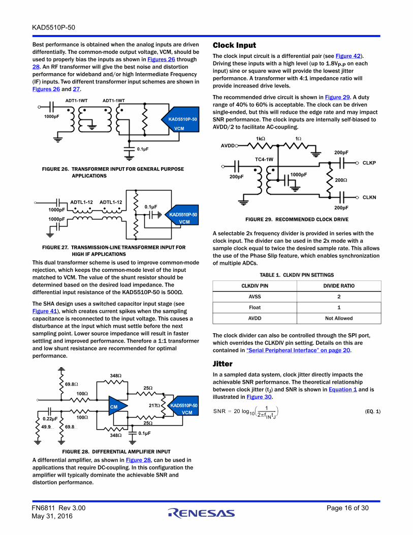
Best performance is obtained when the analog inputs are driven differentially. The common-mode output voltage, VCM, should be used to properly bias the inputs as shown in Figures 26 through 28. An RF transformer will give the best noise and distortion performance for wideband and/or high Intermediate Frequency (IF) inputs. Two different transformer input schemes are shown in Figures 26 and 27.
This dual transformer scheme is used to improve common-mode rejection, which keeps the common-mode level of the input matched to VCM. The value of the shunt resistor should be determined based on the desired load impedance. The differential input resistance of the KAD5510P-50 is 500Ω.
The SHA design uses a switched capacitor input stage (see Figure 41), which creates current spikes when the sampling capacitance is reconnected to the input voltage. This causes a disturbance at the input which must settle before the next sampling point. Lower source impedance will result in faster settling and improved performance. Therefore a 1:1 transformer and low shunt resistance are recommended for optimal performance.
A differential amplifier, as shown in Figure 28, can be used in applications that require DC-coupling. In this configuration the amplifier will typically dominate the achievable SNR and distortion performance.
Clock InputThe clock input circuit is a differential pair (see Figure 42). Driving these inputs with a high level (up to 1.8VP-P on each input) sine or square wave will provide the lowest jitter performance. A transformer with 4:1 impedance ratio will provide increased drive levels.
The recommended drive circuit is shown in Figure 29. A duty range of 40% to 60% is acceptable. The clock can be driven single-ended, but this will reduce the edge rate and may impact SNR performance. The clock inputs are internally self-biased to AVDD/2 to facilitate AC-coupling.
A selectable 2x frequency divider is provided in series with the clock input. The divider can be used in the 2x mode with a sample clock equal to twice the desired sample rate. This allows the use of the Phase Slip feature, which enables synchronization of multiple ADCs.
The clock divider can also be controlled through the SPI port, which overrides the CLKDIV pin setting. Details on this are contained in “Serial Peripheral Interface” on page 20.
JitterIn a sampled data system, clock jitter directly impacts the achievable SNR performance. The theoretical relationship between clock jitter (tJ) and SNR is shown in Equation 1 and is illustrated in Figure 30.
FIGURE 26. TRANSFORMER INPUT FOR GENERAL PURPOSE APPLICATIONS
ADT1-1WT
0.1µF
KAD5510P-50
VCM
ADT1-1WT
1000pF
FIGURE 27. TRANSMISSION-LINE TRANSFORMER INPUT FOR HIGH IF APPLICATIONS
ADTL1-120.1µF
KAD5510P-50
VCM
ADTL1-12
1000pF
1000pF
FIGURE 28. DIFFERENTIAL AMPLIFIER INPUT
KAD5510P-50
VCM
0.1µF
0.22µF
69.849.9
100
100
69.8
348
348
CM 217
25
25
TABLE 1. CLKDIV PIN SETTINGS
CLKDIV PIN DIVIDE RATIO
AVSS 2
Float 1
AVDD Not Allowed
FIGURE 29. RECOMMENDED CLOCK DRIVE
TC4-1W
200pF
AVDD
200
200pF
200pF
CLKP
CLKN
1k 1k
1000pF
SNR 20 log101
2fINtJ-------------------- = (EQ. 1)
FN6811 Rev 3.00 Page 16 of 30May 31, 2016
KAD5510P-50
This relationship shows the SNR that would be achieved if clock jitter were the only non-ideal factor. In reality, achievable SNR is limited by internal factors such as linearity, aperture jitter and thermal noise. Internal aperture jitter is the uncertainty in the sampling instant shown in Figure 2 on page 6. The internal aperture jitter combines with the input clock jitter in a root-sum-square fashion, since they are not statistically correlated, and this determines the total jitter in the system. The total jitter, combined with other noise sources, then determines the achievable SNR.
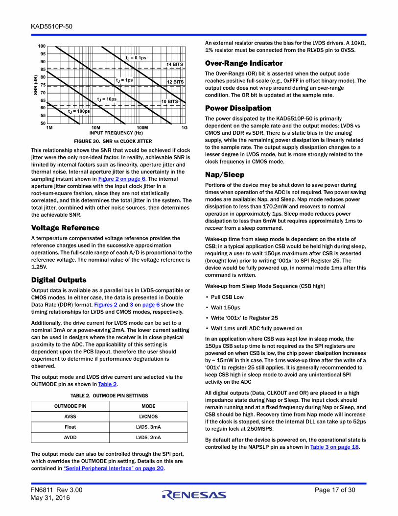
Voltage ReferenceA temperature compensated voltage reference provides the reference charges used in the successive approximation operations. The full-scale range of each A/D is proportional to the reference voltage. The nominal value of the voltage reference is 1.25V.
Digital OutputsOutput data is available as a parallel bus in LVDS-compatible or CMOS modes. In either case, the data is presented in Double Data Rate (DDR) format. Figures 2 and 3 on page 6 show the timing relationships for LVDS and CMOS modes, respectively.
Additionally, the drive current for LVDS mode can be set to a nominal 3mA or a power-saving 2mA. The lower current setting can be used in designs where the receiver is in close physical proximity to the ADC. The applicability of this setting is dependent upon the PCB layout, therefore the user should experiment to determine if performance degradation is observed.
The output mode and LVDS drive current are selected via the OUTMODE pin as shown in Table 2.
The output mode can also be controlled through the SPI port, which overrides the OUTMODE pin setting. Details on this are contained in “Serial Peripheral Interface” on page 20.
An external resistor creates the bias for the LVDS drivers. A 10kΩ, 1% resistor must be connected from the RLVDS pin to OVSS.
Over-Range IndicatorThe Over-Range (OR) bit is asserted when the output code reaches positive full-scale (e.g., 0xFFF in offset binary mode). The output code does not wrap around during an over-range condition. The OR bit is updated at the sample rate.
Power DissipationThe power dissipated by the KAD5510P-50 is primarily dependent on the sample rate and the output modes: LVDS vs CMOS and DDR vs SDR. There is a static bias in the analog supply, while the remaining power dissipation is linearly related to the sample rate. The output supply dissipation changes to a lesser degree in LVDS mode, but is more strongly related to the clock frequency in CMOS mode.
Nap/SleepPortions of the device may be shut down to save power during times when operation of the ADC is not required. Two power saving modes are available: Nap, and Sleep. Nap mode reduces power dissipation to less than 170.2mW and recovers to normal operation in approximately 1µs. Sleep mode reduces power dissipation to less than 6mW but requires approximately 1ms to recover from a sleep command.
Wake-up time from sleep mode is dependent on the state of CSB; in a typical application CSB would be held high during sleep, requiring a user to wait 150µs maximum after CSB is asserted (brought low) prior to writing ‘001x’ to SPI Register 25. The device would be fully powered up, in normal mode 1ms after this command is written.
Wake-up from Sleep Mode Sequence (CSB high)
• Pull CSB Low
• Wait 150µs
• Write ‘001x’ to Register 25
• Wait 1ms until ADC fully powered on
In an application where CSB was kept low in sleep mode, the 150µs CSB setup time is not required as the SPI registers are powered on when CSB is low, the chip power dissipation increases by ~ 15mW in this case. The 1ms wake-up time after the write of a ‘001x’ to register 25 still applies. It is generally recommended to keep CSB high in sleep mode to avoid any unintentional SPI activity on the ADC
All digital outputs (Data, CLKOUT and OR) are placed in a high impedance state during Nap or Sleep. The input clock should remain running and at a fixed frequency during Nap or Sleep, and CSB should be high. Recovery time from Nap mode will increase if the clock is stopped, since the internal DLL can take up to 52µs to regain lock at 250MSPS.
By default after the device is powered on, the operational state is controlled by the NAPSLP pin as shown in Table 3 on page 18.
TABLE 2. OUTMODE PIN SETTINGS
OUTMODE PIN MODE
AVSS LVCMOS
Float LVDS, 3mA
AVDD LVDS, 2mA
FIGURE 30. SNR vs CLOCK JITTER
tJ = 100ps
tJ = 10ps
tJ = 1ps
tJ = 0.1ps
10 BITS
12 BITS
14 BITS
50
55
60
65
70
75
80
85
90
95
100
1M 10M 100M 1G
SN
R (
dB
)
INPUT FREQUENCY (Hz)
FN6811 Rev 3.00 Page 17 of 30May 31, 2016

KAD5510P-50
The power-down mode can also be controlled through the SPI port, which overrides the NAPSLP pin setting. Details on this are contained in “Serial Peripheral Interface” on page 20. This is an indexed function when controlled from the SPI, but a global function when driven from the pin.
Data FormatOutput data can be presented in three formats: two’s complement, Gray code and offset binary. The data format is selected via the OUTFMT pin as shown in Table 4.
The data format can also be controlled through the SPI port, which overrides the OUTFMT pin setting. Details on this are contained in “Serial Peripheral Interface” on page 20.
Offset binary coding maps the most negative input voltage to code 0x000 (all zeros) and the most positive input to 0xFFF (all ones). Two’s complement coding simply complements the MSB of the offset binary representation.
When calculating Gray code, the MSB is unchanged. The remaining bits are computed as the XOR of the current bit position and the next most significant bit. Figure 31 shows this operation.
Converting back to offset binary from Gray code must be done recursively, using the result of each bit for the next lower bit as shown in Figure 32.
Mapping of the input voltage to the various data formats is shown in Table 5.
TABLE 3. NAPSLP PIN SETTINGS
NAPSLP PIN MODE
AVSS Normal
Float Sleep
AVDD Nap
TABLE 4. OUTFMT PIN SETTINGS
OUTFMT PIN MODE
AVSS Offset Binary
Float Two’s Complement
AVDD Gray Code
FIGURE 31. BINARY TO GRAY CODE CONVERSION
89 7 01BINARY
89 7 0GRAY CODE
• • • •
• • • •
• • • •
1
TABLE 5. INPUT VOLTAGE TO OUTPUT CODE MAPPING
INPUT VOLTAGE OFFSET BINARY
TWO’S COMPLEMENT GRAY CODE
–Full Scale 000 00 000 00 100 00 000 00 000 00 000 00
–Full Scale + 1 LSB
000 00 000 01 100 00 000 01 000 00 000 01
Mid–Scale 100 00 000 00 000 00 000 00 110 00 000 00
+Full Scale – 1 LSB
111 11 111 10 011 11 111 10 100 00 000 01
+Full Scale 111 11 111 11 011 11 111 11 100 00 000 00
FIGURE 32. GRAY CODE TO BINARY CONVERSION
89 7 01
BINARY 89 7 0
GRAY CODE • • • •
• • • •
• • • •
1
• • • •
FN6811 Rev 3.00 Page 18 of 30May 31, 2016

KAD5510P-50
FIGURE 33. MSB-FIRST ADDRESSING
CSB
SCLK
SDIO R/W W1 W0 A12 A11 A1 A0 D7 D6 D5 D4 D3 D2 D1 D0A10
FIGURE 34. LSB-FIRST ADDRESSING
CSB
SCLK
SDIO R/WW1W0A12A11A1A0 D7D6D5D4D3D2D1D0A2
FIGURE 35. SPI WRITE
tS
tHI tCLKtLO
R/W W1 W0 A12 A11 A10 A9 A8 A7 D5 D4 D3 D2 D1 D0
tHtDHW
tDSW
SPI WRITE
CSB
SCLK
SDIO
FIGURE 36. SPI READ
(3-WIRE MODE)
(4-WIRE MODE)
R/W W1 W0 A12 A11 A10 A9 A2 A1 D7 D6 D3 D2 D1
D7 D3 D2 D1 D0
A0
WRITING A READ COMMAND READING DATA
D0
tHtDHR
tDVR
SPI READ
tHI tCLKtLO
tDHWtDSW
tSCSB
SCLK
SDIO
SDO
FN6811 Rev 3.00 Page 19 of 30May 31, 2016
KAD5510P-50
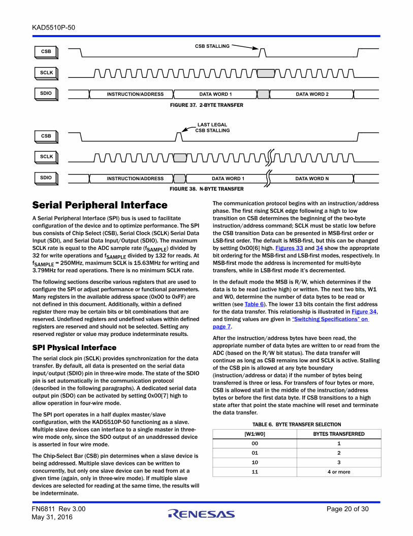
Serial Peripheral InterfaceA Serial Peripheral Interface (SPI) bus is used to facilitate configuration of the device and to optimize performance. The SPI bus consists of Chip Select (CSB), Serial Clock (SCLK) Serial Data Input (SDI), and Serial Data Input/Output (SDIO). The maximum SCLK rate is equal to the ADC sample rate (fSAMPLE) divided by 32 for write operations and fSAMPLE divided by 132 for reads. At fSAMPLE = 250MHz, maximum SCLK is 15.63MHz for writing and 3.79MHz for read operations. There is no minimum SCLK rate.
The following sections describe various registers that are used to configure the SPI or adjust performance or functional parameters. Many registers in the available address space (0x00 to 0xFF) are not defined in this document. Additionally, within a defined register there may be certain bits or bit combinations that are reserved. Undefined registers and undefined values within defined registers are reserved and should not be selected. Setting any reserved register or value may produce indeterminate results.
SPI Physical InterfaceThe serial clock pin (SCLK) provides synchronization for the data transfer. By default, all data is presented on the serial data input/output (SDIO) pin in three-wire mode. The state of the SDIO pin is set automatically in the communication protocol (described in the following paragraphs). A dedicated serial data output pin (SDO) can be activated by setting 0x00[7] high to allow operation in four-wire mode.
The SPI port operates in a half duplex master/slave configuration, with the KAD5510P-50 functioning as a slave. Multiple slave devices can interface to a single master in three-wire mode only, since the SDO output of an unaddressed device is asserted in four wire mode.
The Chip-Select Bar (CSB) pin determines when a slave device is being addressed. Multiple slave devices can be written to concurrently, but only one slave device can be read from at a given time (again, only in three-wire mode). If multiple slave devices are selected for reading at the same time, the results will be indeterminate.
The communication protocol begins with an instruction/address phase. The first rising SCLK edge following a high to low transition on CSB determines the beginning of the two-byte instruction/address command; SCLK must be static low before the CSB transition Data can be presented in MSB-first order or LSB-first order. The default is MSB-first, but this can be changed by setting 0x00[6] high. Figures 33 and 34 show the appropriate bit ordering for the MSB-first and LSB-first modes, respectively. In MSB-first mode the address is incremented for multi-byte transfers, while in LSB-first mode it’s decremented.
In the default mode the MSB is R/W, which determines if the data is to be read (active high) or written. The next two bits, W1 and W0, determine the number of data bytes to be read or written (see Table 6). The lower 13 bits contain the first address for the data transfer. This relationship is illustrated in Figure 34, and timing values are given in “Switching Specifications” on page 7.
After the instruction/address bytes have been read, the appropriate number of data bytes are written to or read from the ADC (based on the R/W bit status). The data transfer will continue as long as CSB remains low and SCLK is active. Stalling of the CSB pin is allowed at any byte boundary (instruction/address or data) if the number of bytes being transferred is three or less. For transfers of four bytes or more, CSB is allowed stall in the middle of the instruction/address bytes or before the first data byte. If CSB transitions to a high state after that point the state machine will reset and terminate the data transfer.
FIGURE 37. 2-BYTE TRANSFER
CSB
SCLK
SDIO INSTRUCTION/ADDRESS DATA WORD 1 DATA WORD 2
CSB STALLING
FIGURE 38. N-BYTE TRANSFER
CSB
SCLK
SDIO INSTRUCTION/ADDRESS DATA WORD 1 DATA WORD N
LAST LEGALCSB STALLING
TABLE 6. BYTE TRANSFER SELECTION
[W1:W0] BYTES TRANSFERRED
00 1
01 2
10 3
11 4 or more
FN6811 Rev 3.00 Page 20 of 30May 31, 2016

KAD5510P-50
Figures 37 and 38 illustrate the timing relationships for 2-byte and N-byte transfers, respectively. The operation for a 3-byte transfer can be inferred from these diagrams.
SPI Configuration
ADDRESS 0x00: CHIP_PORT_CONFIGBit ordering and SPI reset are controlled by this register. Bit order can be selected as MSB to LSB (MSB first) or LSB to MSB (LSB first) to accommodate various microcontrollers.
Bit 7 SDO Active
Bit 6 LSB First
Setting this bit high configures the SPI to interpret serial data as arriving in LSB to MSB order.
Bit 5 Soft Reset
Setting this bit high resets all SPI registers to default values.
Bit 4 Reserved
This bit should always be set high.
Bits 3:0 These bits should always mirror bits 4:7 to avoid ambiguity in bit ordering.
ADDRESS 0x02: BURST_ENDIf a series of sequential registers are to be set, burst mode can improve throughput by eliminating redundant addressing. In 3-wire SPI mode the burst is ended by pulling the CSB pin high. If the device is operated in 2-wire mode the CSB pin is not available. In that case, setting the burst_end address determines the end of the transfer. During a write operation, the user must be cautious to transmit the correct number of bytes based on the starting and ending addresses.
Bits 7:0 Burst End Address
This register value determines the ending address of the burst data.
Device Information
ADDRESS 0x08: CHIP_ID
ADDRESS 0x09: CHIP_VERSIONThe generic die identifier and a revision number, respectively, can be read from these two registers.
Indexed Device Configuration/Control
ADDRESS 0x10: DEVICE_INDEX_ABits 1:0 ADC01, ADC00
Determines which ADC is addressed. Valid states for this register are 0x01 or 0x10. The two ADC cores cannot be adjusted concurrently.
A common SPI map, which can accommodate single-channel or multi-channel devices, is used for all Intersil ADC products. Certain configuration commands (identified as Indexed in the SPI map) can be executed on a per-converter basis. This register determines which converter is being addressed for an Indexed command. It is
important to note that only a single converter can be addressed at a time.
This register defaults to 00h, indicating that no ADC is addressed. Error code ‘AD’ is returned if any indexed register is read from without properly setting device_index_A.
ADDRESS 0x20: OFFSET_COARSE
ADDRESS 0x21: OFFSET_FINEThe input offset of the ADC core can be adjusted in fine and coarse steps. Both adjustments are made via an 8-bit word as detailed in Table 7. The data format is two’s complement.
The default value of each register will be the result of the self-calibration after initial power-up. If a register is to be incremented or decremented, the user should first read the register value then write the incremented or decremented value back to the same register.
ADDRESS 0x22: GAIN_COARSE
ADDRESS 0x23: GAIN_MEDIUM
ADDRESS 0x24: GAIN_FINEGain of the ADC core can be adjusted in coarse, medium and fine steps. Coarse gain is a 4-bit adjustment while medium and fine are 8-bit. Multiple Coarse Gain Bits can be set for a total adjustment range of ±4.2%. (‘0011’ -4.2% and ‘1100’ +4.2%) It is recommended to use one of the coarse gain settings (-4.2%, -2.8%, -1.4%, 0, 1.4%, 2.8%, 4.2%) and fine-tune the gain using the registers at 23h and 24h.
The default value of each register will be the result of the self-calibration after initial power-up. If a register is to be incremented or decremented, the user should first read the register value then write the incremented or decremented value back to the same register.
TABLE 7. OFFSET ADJUSTMENTS
PARAMETER0x20[7:0]
COARSE OFFSET0x21[7:0]
FINE OFFSET
Steps 255 255
-Full Scale (0x00) -133 LSB (-47mV) -5 LSB (-1.75mV)
Mid–Scale (0x80) 0.0 LSB (0.0mV) 0.0LSB
+Full Scale (0xFF) +133 LSB (+47mV) +5 LSB (+1.75mV)
Nominal Step Size 1.04 LSB (0.37mV) 0.04 LSB (0.014mV)
TABLE 8. COARSE GAIN ADJUSTMENT
0x22[3:0]NOMINAL COARSE GAIN ADJUST
(%)
Bit3 +2.8
Bit2 +1.4
Bit1 -2.8
Bit0 -1.4
FN6811 Rev 3.00 Page 21 of 30May 31, 2016
KAD5510P-50
ADDRESS 0x25: MODESTwo distinct reduced power modes can be selected. By default, the tri-level NAPSLP pin can select normal operation, nap or sleep modes (refer to “Nap/Sleep” on page 17). This functionality can be overridden and controlled through the SPI. This is an indexed function when controlled from the SPI, but a global function when driven from the pin. This register is not changed by a soft reset.
Global Device Configuration/Control
ADDRESS 0x70: SKEW_DIFFThe value in the skew_diff register adjusts the timing skew between the two ADCs cores. The nominal range and resolution of this adjustment are given in Table 11. The default value of this register after power-up is 80h.
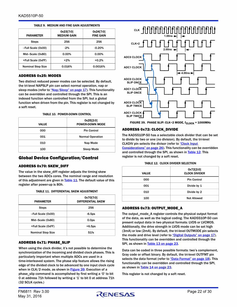
ADDRESS 0x71: PHASE_SLIPWhen using the clock divider, it’s not possible to determine the synchronization of the incoming and divided clock phases. This is particularly important when multiple ADCs are used in a time-interleaved system. The phase slip feature allows the rising edge of the divided clock to be advanced by one input clock cycle when in CLK/2 mode, as shown in Figure 39. Execution of a phase_slip command is accomplished by first writing a ‘0’ to bit 0 at address 71h followed by writing a ‘1’ to bit 0 at address 71h (32 SCLK cycles.)
ADDRESS 0x72: CLOCK_DIVIDEThe KAD5510P-50 has a selectable clock divider that can be set to divide by two or one (no division). By default, the tri-level CLKDIV pin selects the divisor (refer to “Clock Input Considerations” on page 26). This functionality can be overridden and controlled through the SPI, as shown in Table 12. This register is not changed by a soft reset.
ADDRESS 0x73: OUTPUT_MODE_AThe output_mode_A register controls the physical output format of the data, as well as the logical coding. The KAD5510P-50 can present output data in two physical formats: LVDS or LVCMOS. Additionally, the drive strength in LVDS mode can be set high (3mA) or low (2mA). By default, the tri-level OUTMODE pin selects the mode and drive level (refer to “Digital Outputs” on page 17). This functionality can be overridden and controlled through the SPI, as shown in Table 13 on page 23.
Data can be coded in three possible formats: two’s complement, Gray code or offset binary. By default, the tri-level OUTFMT pin selects the data format (refer to “Data Format” on page 18). This functionality can be overridden and controlled through the SPI, as shown in Table 14 on page 23.
This register is not changed by a soft reset.
TABLE 9. MEDIUM AND FINE GAIN ADJUSTMENTS
PARAMETER0x23[7:0]
MEDIUM GAIN0x24[7:0]FINE GAIN
Steps 256 256
–Full Scale (0x00) -2% -0.20%
Mid–Scale (0x80) 0.00% 0.00%
+Full Scale (0xFF) +2% +0.2%
Nominal Step Size 0.016% 0.0016%
TABLE 10. POWER-DOWN CONTROL
VALUE0x25[2:0]
POWER-DOWN MODE
000 Pin Control
001 Normal Operation
010 Nap Mode
100 Sleep Mode
TABLE 11. DIFFERENTIAL SKEW ADJUSTMENT
PARAMETER0x70[7:0]
DIFFERENTIAL SKEW
Steps 256
–Full Scale (0x00) -6.5ps
Mid–Scale (0x80) 0.0ps
+Full Scale (0xFF) +6.5ps
Nominal Step Size 51fs
TABLE 12. CLOCK DIVIDER SELECTION
VALUE0x72[2:0]
CLOCK DIVIDER
000 Pin Control
001 Divide by 1
010 Divide by 2
100 Not Allowed
FIGURE 39. PHASE SLIP: CLK÷2 MODE, fCLOCK = 1000MHz
CLK
CLK÷2
ADC0 CLOCKSLIP ONCE
ADC0 CLOCKSLIP TWICE
ADC1 CLOCKSLIP ONCE
ADC1 CLOCKSLIP TWICE
ADC0 CLOCK
ADC1 CLOCK
1.00ns
2.00ns
4.00ns
FN6811 Rev 3.00 Page 22 of 30May 31, 2016
KAD5510P-50
ADDRESS 0x74: OUTPUT_MODE_B
ADDRESS 0x75: CONFIG_STATUSBit 6 DLL Range
This bit sets the DLL operating range to fast (default) or slow.
Internal clock signals are generated by a delay-locked loop (DLL), which has a finite operating range. Table 15 shows the allowable sample rate ranges for the slow and fast settings.
The output_mode_B and config_status registers are used in conjunction to enable DDR mode and select the frequency range of the DLL clock generator. The method of setting these options is different from the other registers.
The procedure for setting output_mode_B is shown in Figure 40. Read the contents of output_mode_B and config_status and XOR them. Then XOR this result with the desired value for output_mode_B and write that XOR result to the register.
Device TestThe KAD5510P-50 can produce preset or user defined patterns on the digital outputs to facilitate in-situ testing. A static word can be placed on the output bus, or two different words can alternate. In the alternate mode, the values defined as Word 1
and Word 2 (as shown in Table 16) are set on the output bus on alternating clock phases. The test mode is enabled asynchronously to the sample clock, therefore several sample clock cycles may elapse before the data is present on the output bus.
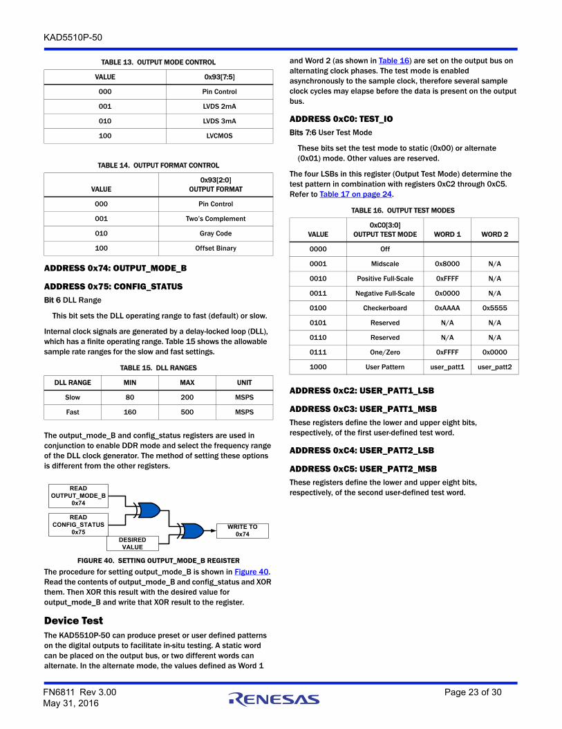
ADDRESS 0xC0: TEST_IOBits 7:6 User Test Mode
These bits set the test mode to static (0x00) or alternate (0x01) mode. Other values are reserved.
The four LSBs in this register (Output Test Mode) determine the test pattern in combination with registers 0xC2 through 0xC5. Refer to Table 17 on page 24.
ADDRESS 0xC2: USER_PATT1_LSB
ADDRESS 0xC3: USER_PATT1_MSBThese registers define the lower and upper eight bits, respectively, of the first user-defined test word.
ADDRESS 0xC4: USER_PATT2_LSB
ADDRESS 0xC5: USER_PATT2_MSBThese registers define the lower and upper eight bits, respectively, of the second user-defined test word.
TABLE 13. OUTPUT MODE CONTROL
VALUE 0x93[7:5]
000 Pin Control
001 LVDS 2mA
010 LVDS 3mA
100 LVCMOS
TABLE 14. OUTPUT FORMAT CONTROL
VALUE0x93[2:0]
OUTPUT FORMAT
000 Pin Control
001 Two’s Complement
010 Gray Code
100 Offset Binary
TABLE 15. DLL RANGES
DLL RANGE MIN MAX UNIT
Slow 80 200 MSPS
Fast 160 500 MSPS
FIGURE 40. SETTING OUTPUT_MODE_B REGISTER
READ CONFIG_STATUS
0x75
READ OUTPUT_MODE_B
0x74
DESIRED VALUE
WRITE TO0x74
TABLE 16. OUTPUT TEST MODES
VALUE0xC0[3:0]
OUTPUT TEST MODE WORD 1 WORD 2
0000 Off
0001 Midscale 0x8000 N/A
0010 Positive Full-Scale 0xFFFF N/A
0011 Negative Full-Scale 0x0000 N/A
0100 Checkerboard 0xAAAA 0x5555
0101 Reserved N/A N/A
0110 Reserved N/A N/A
0111 One/Zero 0xFFFF 0x0000
1000 User Pattern user_patt1 user_patt2
FN6811 Rev 3.00 Page 23 of 30May 31, 2016

KAD5510P-50
TABLE 17. SPI MEMORY MAP
ADDR(HEX)
PARAMETERNAME
BIT 7(MSB) BIT 6 BIT 5 BIT 4 BIT 3 BIT 2 BIT 1
BIT 0 (LSB)
DEF. VALUE (HEX)
INDEXED/GLOBAL
SP
I CO
NFI
G
00 port_config SDOActive
LSB First
Soft Reset
Mirror (bit5)
Mirror (bit6)
Mirror (bit7)
00h G
01 Reserved Reserved
02 burst_end Burst end address [7:0] 00h G
03-07 Reserved Reserved
INFO
08 chip_id Chip ID # Read only G
09 chip_version Chip Version # Read only G
IND
EXED
DEV
ICE
CO
NFI
G/C
ON
TRO
L
10 device_index_A Reserved ADC01 ADC00 00h I
11-1F Reserved Reserved
20 offset_coarse Coarse Offset Cal. value I
21 offset_fine Fine Offset Cal. value I
22 gain_coarse Reserved Coarse Gain Cal. value I
23 gain_medium Medium Gain Cal. value I
24 gain_fine Fine Gain Cal. value I
25 modes Reserved Power-Down Mode [2:0] 000 = Pin Control 001 = Normal Operation 010 = Nap 100 = Sleep Other codes = Reserved
00h NOT
affected by soft
reset
I
26-5F Reserved Reserved
60-6F Reserved Reserved
GLO
BA
L D
EVIC
ECO
NFI
G/C
ON
TRO
L
70 skew_diff Differential Skew 80h
71 phase_slip Reserved Next ClockEdge
00h G
72 clock_divide Clock Divide [2:0]000 = Pin Control 001 = divide by 1 010 = divide by 2 100 = divide by 4 Other codes = Reserved
00h NOT
affected by soft reset
G
73 output_mode_A Output Mode [2:0] 000 = Pin Control 001 = LVDS 2mA 010 = LVDS 3mA 100 = LVCMOS other codes = Reserved
Output Format [2:0] 000 = Pin Control 001 = Twos Complement 010 = Gray Code 100 = Offset Binary Other codes = Reserved
00h NOT
affected by soft reset
G
74 output_mode_B DLL Range
0 = fast 1 = slow
00h NOT
affected by soft
reset
G
75 config_status XOR Result
Read Only G
76-BF Reserved Reserved
FN6811 Rev 3.00 Page 24 of 30May 31, 2016
KAD5510P-50
Dev
ice
Test
C0 test_io User Test Mode[1:0]
00 = Single 01 = Alternate10 = Reserved11 = Reserved
Output Test Mode [3:0] 00h G
0 = Off 1 = Midscale Short 2 = +FS Short 3 = -FS Short 4 = Checker Board 5 = Reserved 6 = Reserved
7 = One/Zero Word Toggle 8 = User Input 9-15 = Reserved
C1 Reserved Reserved 00h G
C2 user_patt 1_lsb B7 B6 B5 B4 B3 B2 B1 B0 00h G
C3 user_patt1_msb B15 B14 B13 B12 B11 B10 B9 B8 00h G
C4 user_patt 2_lsb B7 B6 B5 B4 B3 B2 B1 B0 00h G
C5 user_patt2_msb B15 B14 B13 B12 B11 B10 B9 B8 00h G
C6-FF Reserved Reserved
TABLE 17. SPI MEMORY MAP (Continued)
ADDR(HEX)
PARAMETERNAME
BIT 7(MSB) BIT 6 BIT 5 BIT 4 BIT 3 BIT 2 BIT 1
BIT 0 (LSB)
DEF. VALUE (HEX)
INDEXED/GLOBAL
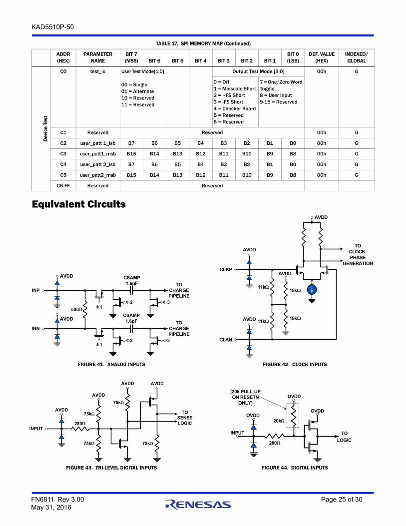
Equivalent Circuits
FIGURE 41. ANALOG INPUTS FIGURE 42. CLOCK INPUTS
FIGURE 43. TRI-LEVEL DIGITAL INPUTS FIGURE 44. DIGITAL INPUTS
AVDD
INP
INN
AVDD
F 1
F 1
F 2 F 3
F 2 F 3
CSAMP1.6pF
CSAMP1.6pF TO
CHARGE PIPELINE
TO CHARGE PIPELINE
500
AVDD
CLKP
CLKN
AVDD
AVDD
TOCLOCK-PHASE
GENERATION
11k
11k
AVDD
18k
18k
AVDD
INPUT
AVDD
AVDD AVDD
TO SENSE LOGIC
75k
75k
75k75k
280
INPUT
OVDDOVDD
280
TO
LOGIC
20k
OVDD(20k PULL-UP ON RESETN
ONLY)
FN6811 Rev 3.00 Page 25 of 30May 31, 2016
KAD5510P-50
ADC Evaluation PlatformIntersil offers an ADC Evaluation platform which can be used to evaluate any of the KADxxxxx ADC family. The platform consists of a FPGA based data capture motherboard and a family of ADC daughtercards. This USB based platform allows a user to quickly evaluate the ADC’s performance at a user’s specific application frequency requirements. More information is available at http://www.intersil.com/converters/adc_eval_platform/.
Layout ConsiderationsSplit Ground and Power PlanesData converters operating at high sampling frequencies require extra care in PC board layout. Many complex board designs benefit from isolating the analog and digital sections. Analog supply and ground planes should be laid out under signal and clock inputs. Locate the digital planes under outputs and logic pins. Grounds should be joined under the chip.
Clock Input ConsiderationsUse matched transmission lines to the transformer inputs for the analog input and clock signals. Locate transformers and terminations as close to the chip as possible.
Exposed PaddleThe exposed paddle must be electrically connected to analog ground (AVSS) and should be connected to a large copper plane using numerous vias for optimal thermal performance.
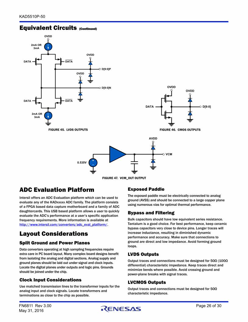
Bypass and FilteringBulk capacitors should have low equivalent series resistance. Tantalum is a good choice. For best performance, keep ceramic bypass capacitors very close to device pins. Longer traces will increase inductance, resulting in diminished dynamic performance and accuracy. Make sure that connections to ground are direct and low impedance. Avoid forming ground loops.
LVDS OutputsOutput traces and connections must be designed for 50Ω (100Ω differential) characteristic impedance. Keep traces direct and minimize bends where possible. Avoid crossing ground and power-plane breaks with signal traces.
LVCMOS OutputsOutput traces and connections must be designed for 50Ω characteristic impedance.
FIGURE 45. LVDS OUTPUTS FIGURE 46. CMOS OUTPUTS
FIGURE 47. VCM_OUT OUTPUT
Equivalent Circuits (Continued)
D[9:0]P
OVDD
OVDD
2mA OR3mA
2mA OR3mA
DATA
DATA
DATA
DATA
D[9:0]N
OVDD
D[9:0]
OVDDOVDD
DATA
VCM
AVDD
0.535V+
–
FN6811 Rev 3.00 Page 26 of 30May 31, 2016

KAD5510P-50
Unused InputsStandard logic inputs (RESETN, CSB, SCLK, SDIO, SDO) which will not be operated do not require connection to ensure optimal ADC performance. These inputs can be left floating if they are not used. Tri-level inputs (NAPSLP, OUTMODE, OUTFMT, CLKDIV) accept a floating input as a valid state, and therefore should be biased according to the desired functionality.
DefinitionsAnalog Input Bandwidth is the analog input frequency at which the spectral output power at the fundamental frequency (as determined by FFT analysis) is reduced by 3dB from its full-scale low-frequency value. This is also referred to as Full Power Bandwidth.
Aperture Delay or Sampling Delay is the time required after the rise of the clock input for the sampling switch to open, at which time the signal is held for conversion.
Aperture Jitter is the RMS variation in aperture delay for a set of samples.
Clock Duty Cycle is the ratio of the time the clock wave is at logic high to the total time of one clock period.
Differential Nonlinearity (DNL) is the deviation of any code width from an ideal 1 LSB step.
Effective Number of Bits (ENOB) is an alternate method of specifying Signal to Noise-and-Distortion Ratio (SINAD). In dB, it is calculated as: ENOB = (SINAD - 1.76)/6.02
Gain Error is the ratio of the difference between the voltages that cause the lowest and highest code transitions to the full-scale voltage less 2 LSB. It is typically expressed in percent.
Integral Nonlinearity (INL) is the maximum deviation of the ADC’s transfer function from a best fit line determined by a least squares curve fit of that transfer function, measured in units of LSBs.
Least Significant Bit (LSB) is the bit that has the smallest value or weight in a digital word. Its value in terms of input voltage is VFS/(2N-1) where N is the resolution in bits.
Missing Codes are output codes that are skipped and will never appear at the ADC output. These codes cannot be reached with any input value.
Most Significant Bit (MSB) is the bit that has the largest value or weight.
Pipeline Delay is the number of clock cycles between the initiation of a conversion and the appearance at the output pins of the data.
Power Supply Rejection Ratio (PSRR) is the ratio of the observed magnitude of a spur in the ADC FFT, caused by an AC signal superimposed on the power supply voltage.
Signal to Noise and Distortion (SINAD) is the ratio of the RMS signal amplitude to the RMS sum of all other spectral components below one half the clock frequency, including harmonics but excluding DC.
Signal-to-Noise Ratio (without Harmonics) is the ratio of the RMS signal amplitude to the RMS sum of all other spectral components below one-half the sampling frequency, excluding harmonics and DC.
SNR and SINAD are either given in units of dB when the power of the fundamental is used as the reference, or dBFS (dB to full scale) when the converter’s full-scale input power is used as the reference.
Spurious Free Dynamic Range (SFDR) is the ratio of the RMS signal amplitude to the RMS value of the largest spurious spectral component. The largest spurious spectral component may or may not be a harmonic.
FN6811 Rev 3.00 Page 27 of 30May 31, 2016
KAD5510P-50
Revision History The revision history provided is for informational purposes only and is believed to be accurate, but not warranted. Please go to the web to make sure that you have the latest revision.
DATE REVISION CHANGE
May 31, 2016 FN6811.3 Increased maximum currents and NAP power dissipation as follows:IAVDD Max from 178 to 188NAP mode power Max from 163 to 170.2Updated 163 to 170.2 in “Nap/Sleep” on page 17.Added About Intersil section.
May 8, 2009 FN6811.2 1)Added nap mode, sleep mode wake up times to spec table2) Added CSB,SCLK Setup time specs for nap,sleep modes to spec table3) Changed SPI setup spec wording inspec table4) Change to pin description table for clarification5) Added thermal pad note6) Updated fig 23 and fig 24 and description in text.7) Update multiple device usage note on at “SPI Physical Interface” on page 208) Added ‘Reserved’ to SPI memory mapat address 25H9) Added section on “ADC Evaluation Platform” on page 2610) Updated table “DIFFERENTIAL SKEW ADJUSTMENT” on page 22.11) Intersil Standards - Added Pb-free reflow link12) Changed to SPI interface section in spec table, timing in cycles now, added write, read specific timing specs.13) Updated SPI timing diagrams, Figures 35, 3614) Updated wakeup time description in “Nap/Sleep” on page 17.15) Updated sleep mode power spec16) Changed label in Figure 4417) Updated cal paragraph in user initiated reset section per DCChanged standard over-temp from “Parameters with MIN and/or MAX limits are 100% tested at +25°C, unless otherwise specified. Temperature limits established by characterization and are not production tested” TO “Parameters with Min and/or MAX limits are 100% production tested at their worst case temperature extreme (+85°C) per Jeff Rogers and Gary Hendrickson.” Updated Note references in Electrical Spec Table.
January 19, 2009 FN6811.1 P1; revised Key SpecsP2; added Part Marking column to Order InfoP4; Moved Thermal Impedance under Thermal Info (used to be on p. 7). Added Theta JA Note 2.P4-7; edits throughout the Specs table. Added Notes 8 and 9. Revised Notes 6 and 7.P7; Removed ESD sectionP10-12; revised Performance Curves throughoutP14; User Initiated Reset section; revised 2nd sentence of 1st paragraphP16; Nap/Sleep; revised 3rd and 4th sentences of 1st paragraphP19; Serial Peripheral Interface; revised 2nd to last sentence of 1st paragraph. SPI Physical Interface; revised 2nd and 3rd sentences of 4th paragraphP20; added last 2 sentences to 1st paragraph of "ADDRESS 0X24: GAIN_FINE". Revised Table 8P21; revised last 2 sentences of "ADDRESS 0X71: PHASE_SLIP". Removed Figure of "PHASE SLIP: CLK÷1 MODE, fCLOCK = 500MHz"P24; revised Figure 43P24; Table 17; revised Bits7:4, Addr C0 Throughout; formatted graphics to Intersil standards
August 6, 2008 FN6811.1 Initial Release
December 5, 2008 FN6811.0 Converted to intersil template. Assigned file number FN6811. Rev 0 - first release (as preliminary datasheet) with new file number.
FN6811 Rev 3.00 Page 28 of 30May 31, 2016

KAD5510P-50
Intersil products are manufactured, assembled and tested utilizing ISO9001 quality systems as notedin the quality certifications found at www.intersil.com/en/support/qualandreliability.html
Intersil products are sold by description only. Intersil may modify the circuit design and/or specifications of products at any time without notice, provided that such modification does not, in Intersil's sole judgment, affect the form, fit or function of the product. Accordingly, the reader is cautioned to verify that datasheets are current before placing orders. Information furnished by Intersil is believed to be accurate and reliable. However, no responsibility is assumed by Intersil or its subsidiaries for its use; nor for any infringements of patents or other rights of third parties which may result from its use. No license is granted by implication or otherwise under any patent or patent rights of Intersil or its subsidiaries.
For information regarding Intersil Corporation and its products, see www.intersil.com
For additional products, see www.intersil.com/en/products.html
© Copyright Intersil Americas LLC 2008-2016. All Rights Reserved.All trademarks and registered trademarks are the property of their respective owners.
About IntersilIntersil Corporation is a leading provider of innovative power management and precision analog solutions. The company's products address some of the largest markets within the industrial and infrastructure, mobile computing and high-end consumer markets.
For the most updated datasheet, application notes, related documentation and related parts, please see the respective product information page found at www.intersil.com.
You may report errors or suggestions for improving this datasheet by visiting www.intersil.com/ask.
Reliability reports are also available from our website at www.intersil.com/support.
FN6811 Rev 3.00 Page 29 of 30May 31, 2016
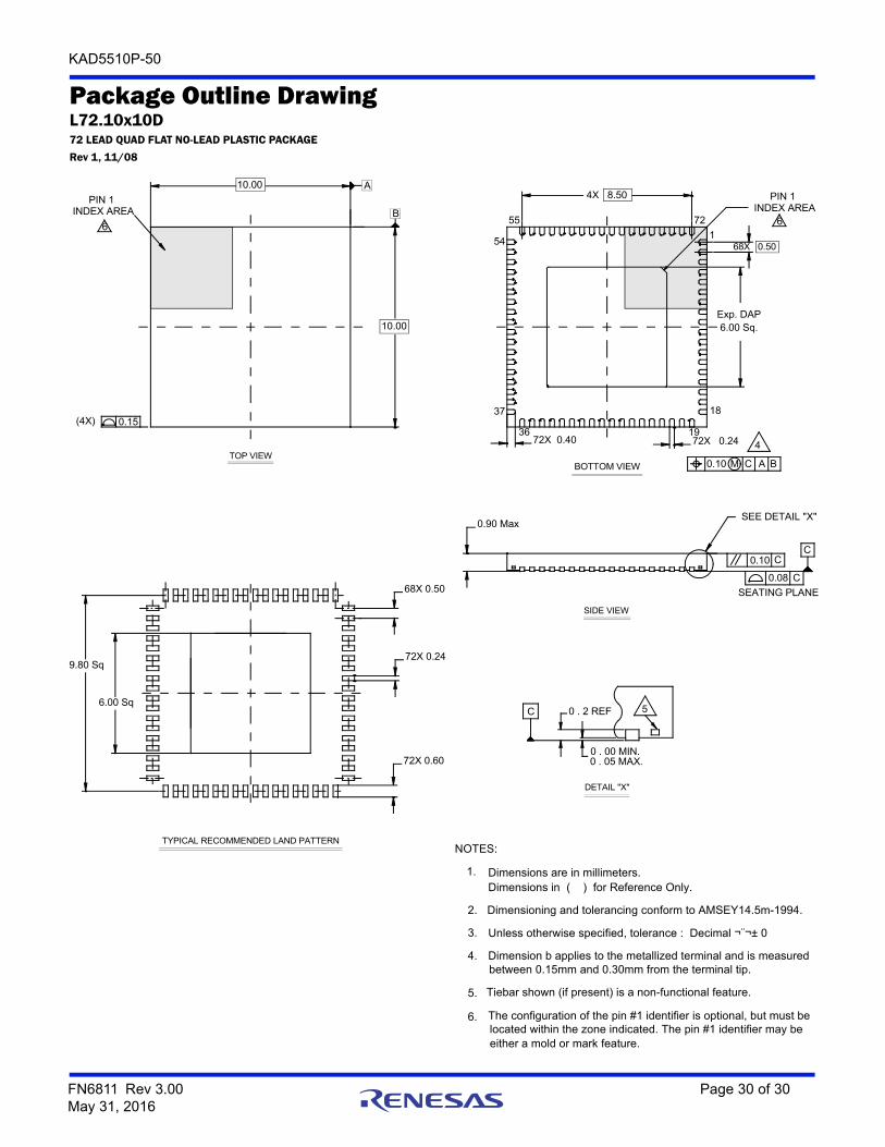
KAD5510P-50
FN6811 Rev 3.00 Page 30 of 30May 31, 2016
Package Outline DrawingL72.10x10D72 LEAD QUAD FLAT NO-LEAD PLASTIC PACKAGE
Rev 1, 11/08
located within the zone indicated. The pin #1 identifier may be
Unless otherwise specified, tolerance : Decimal ± 0
Tiebar shown (if present) is a non-functional feature.
The configuration of the pin #1 identifier is optional, but must be
between 0.15mm and 0.30mm from the terminal tip.Dimension b applies to the metallized terminal and is measured
Dimensions in ( ) for Reference Only.
Dimensioning and tolerancing conform to AMSEY14.5m-1994.
6.
either a mold or mark feature.
3.
5.
4.
2.
Dimensions are in millimeters.1.
NOTES:
DETAIL "X"
SIDE VIEW
TYPICAL RECOMMENDED LAND PATTERN
TOP VIEWBOTTOM VIEW
C 0 . 2 REF
0 . 05 MAX.0 . 00 MIN.
5
B6
PIN 1INDEX AREA
18
1
36 19
0.10 AM C B
4
A4X 8.50
72X 0.40 72X 0.24
68X 0.50
10.00
10.00
0.90 Max
72X 0.24
72X 0.60
68X 0.50
6.00 Sq
9.80 Sq
6
PIN 1INDEX AREA
Exp. DAP6.00 Sq.
SEE DETAIL "X"
SEATING PLANE
0.08
0.10C
C
C
(4X) 0.1537
54
7255