Embed Size (px)
Citation preview

7/25/2019 juction field transistor
http://slidepdf.com/reader/full/juction-field-transistor 1/32
Storey: Electrical & Electronic Systems © Pearson Education Limited 2004 OHT 20.1
Field-Effect Transistors
Introduction
An Overview of ield!Effect "ransistors
Insulated!#ate ield!Effect "ransistors
$unction!#ate ield!Effect "ransistors
E" %aracteristics
Summary of E" %aracteristics
E" Am'lifiers Oter E" A''lications
%a'ter 20

7/25/2019 juction field transistor
http://slidepdf.com/reader/full/juction-field-transistor 2/32
Storey: Electrical & Electronic Systems © Pearson Education Limited 2004 OHT 20.2
Introduction
Field-effect transistors (FETs) are 'ro*a*ly te
sim'lest form of transistor
+ widely used in *ot analo,ue and di,ital a''lications
+ tey are caracterised *y a very i, in'ut resistance
and small 'ysical si-e. and tey can *e used to form
circuits wit a low 'ower consum'tion
+ tey are widely used in very large-scale integration + two *asic forms:
insulated gate FETs
junction gate FETs
20/

7/25/2019 juction field transistor
http://slidepdf.com/reader/full/juction-field-transistor 3/32
Storey: Electrical & Electronic Systems © Pearson Education Limited 2004 OHT 20.3
An Overvie of Field-Effect Transistors
1any forms. *ut *asic o'eration is te same
+ a volta,e on a control in'ut 'roduces an electric field
tat affects te current *etween two oter terminals
+ wen considerin,
am'lifiers we looed
at a circuit usin, a
3control device
+ a E" is a suita*le
control device
20/2

7/25/2019 juction field transistor
http://slidepdf.com/reader/full/juction-field-transistor 4/32
Storey: Electrical & Electronic Systems © Pearson Education Limited 2004 OHT 20.!
"otation
+ E"s are 5 terminal devices drain (d)
source (s) ,ate(,)
+ te ,ate is te control in'ut
+ dia,ram illustrates te
notation used for la*ellin,volta,es and currents

7/25/2019 juction field transistor
http://slidepdf.com/reader/full/juction-field-transistor 5/32
Storey: Electrical & Electronic Systems © Pearson Education Limited 2004 OHT 20.#
Insulated-$ate Field-Effect Transistors
Suc devices are sometimes called I$FETs
(insulated!,ate field!effect transistors) or sometimes
%O&FETs (metal o6ide semiconductor field!effect
transistors)
7i,ital circuits constructed usin, tese devices are
usually descri*ed as usin, %O& tec'nology
8ere we will descri*e tem as 1OSE"s
20/5
7/25/2019 juction field transistor
http://slidepdf.com/reader/full/juction-field-transistor 6/32
Storey: Electrical & Electronic Systems © Pearson Education Limited 2004 OHT 20.(
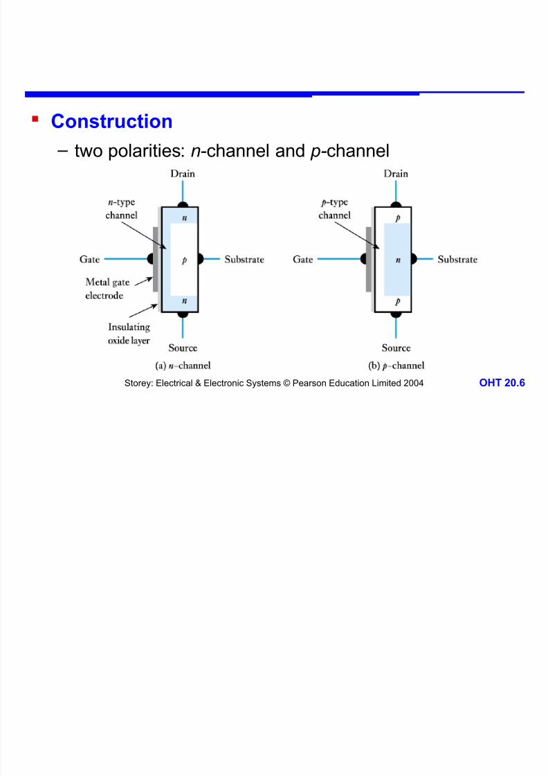
)onstruction
+ two 'olarities: n!cannel and p-cannel

7/25/2019 juction field transistor
http://slidepdf.com/reader/full/juction-field-transistor 7/32
Storey: Electrical & Electronic Systems © Pearson Education Limited 2004 OHT 20.*
O+eration
+ ,ate volt controls te ticness of te cannel
+ consider an n!cannel device
main, te ,ate more positive attracts electrons tote ,ate and maes te ,ate re,ion thicker +reducin, te resistance of te cannel/ "e cannelis said to *e en'anced
main, te ,ate more negative re'els electronsfrom te ,ate and maes te ,ate re,ion thinner +increasin, te resistance of te cannel/ "ecannel is said to *e de+leted

7/25/2019 juction field transistor
http://slidepdf.com/reader/full/juction-field-transistor 8/32
Storey: Electrical & Electronic Systems © Pearson Education Limited 2004 OHT 20.,
+ te effect of varyin, te ,ate volta,e

7/25/2019 juction field transistor
http://slidepdf.com/reader/full/juction-field-transistor 9/32
Storey: Electrical & Electronic Systems © Pearson Education Limited 2004 OHT 20.
+ ,ates as descri*ed a*ove are termed 7e'letion!
Enancement 1OSE"s or sim'ly E %O&FETs
+ some 1OSE"s are constructed so tat in te
a*sence of any ,ate volta,e tere is no cannel suc devices can *e o'erated in an enancement mode. *ut
not in a de'letion mode (since tere is no cannel to de'lete)
tese are called En'ance/ent %O&FETs
+ *ot forms of 1OSE" are availa*le as eitern!cannel or p!cannel devices

7/25/2019 juction field transistor
http://slidepdf.com/reader/full/juction-field-transistor 10/32
Storey: Electrical & Electronic Systems © Pearson Education Limited 2004 OHT 20.10
%O&FET
circuit sy/ols

7/25/2019 juction field transistor
http://slidepdf.com/reader/full/juction-field-transistor 11/32
Storey: Electrical & Electronic Systems © Pearson Education Limited 2004 OHT 20.11
unction-$ate Field-Effect Transistors
Sometimes nown as a $FET
8ere we will use anoter common name + te FET
8ere te insulated ,ate of a 1OSE" is re'lacedwit a reverse!*iased pn 9unction
Since te ,ate 9unction is always reverse!*iased no
current flows into te ,ate and it acts as if it were
insulated
20/4

7/25/2019 juction field transistor
http://slidepdf.com/reader/full/juction-field-transistor 12/32
Storey: Electrical & Electronic Systems © Pearson Education Limited 2004 OHT 20.12
)onstruction
+ two 'olarities: n!cannel and p-cannel

7/25/2019 juction field transistor
http://slidepdf.com/reader/full/juction-field-transistor 13/32
Storey: Electrical & Electronic Systems © Pearson Education Limited 2004 OHT 20.13
O+eration
+ te reverse!*iased ,ate 9unction 'roduced a de'letionlayer in te re,ion of te cannel
+ te ,ate volt controls te ticness of te de'letionlayer and ence te ticness of te cannel
+ consider an n!cannel device te ,ate will always *e ne,ative wit res'ect to te source to
ee' te 9unction *etween te ,ate and te cannel reverse!
*iased main, te ,ate more negative increases te ticness of te
de'letion layer. reducin, te widt of te cannel + increasing te resistance of te cannel/

7/25/2019 juction field transistor
http://slidepdf.com/reader/full/juction-field-transistor 14/32
Storey: Electrical & Electronic Systems © Pearson Education Limited 2004 OHT 20.1!
+ te effect of varyin, te ,ate volta,e

7/25/2019 juction field transistor
http://slidepdf.com/reader/full/juction-field-transistor 15/32
Storey: Electrical & Electronic Systems © Pearson Education Limited 2004 OHT 20.1#
FET circuit sy/ols

7/25/2019 juction field transistor
http://slidepdf.com/reader/full/juction-field-transistor 16/32
Storey: Electrical & Electronic Systems © Pearson Education Limited 2004 OHT 20.1(
FET )'aracteristics
ile 1OSE"s and $E"s o'erate in different
ways. teir caracteristics are ;uite similar
In+ut c'aracteristics
+ in *ot 1OSE"s and $E"s te ,ate is effectively
insulated from te remainder of te device
Out+ut c'aracteristics
+ consider n!cannel devices
+ usually te drain is more 'ositive tan te source
+ te drain volta,e affects te ticness of te cannel
20/<

7/25/2019 juction field transistor
http://slidepdf.com/reader/full/juction-field-transistor 17/32
Storey: Electrical & Electronic Systems © Pearson Education Limited 2004 OHT 20.1*

7/25/2019 juction field transistor
http://slidepdf.com/reader/full/juction-field-transistor 18/32
Storey: Electrical & Electronic Systems © Pearson Education Limited 2004 OHT 20.1,
FET out+ut c'aracteristics

7/25/2019 juction field transistor
http://slidepdf.com/reader/full/juction-field-transistor 19/32
Storey: Electrical & Electronic Systems © Pearson Education Limited 2004 OHT 20.1
Transfer c'aracteristics
+ similar sa'e for all forms of E" + *ut wit a different
offset
+ not a linear res'onse. *ut over a small re,ion mi,t *econsidered to a''ro6imate a linear res'onse
7/25/2019 juction field transistor
http://slidepdf.com/reader/full/juction-field-transistor 20/32
Storey: Electrical & Electronic Systems © Pearson Education Limited 2004 OHT 20.20
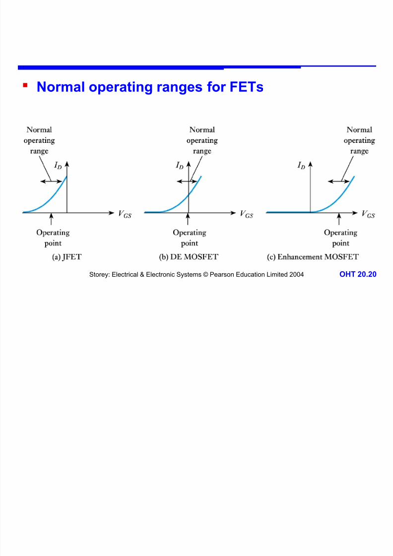
"or/al o+erating ranges for FETs

7/25/2019 juction field transistor
http://slidepdf.com/reader/full/juction-field-transistor 21/32
Storey: Electrical & Electronic Systems © Pearson Education Limited 2004 OHT 20.21
en o'eratin, a*out its o+erating +oint we can
descri*e te transfer caracteristic *y te change in
out'ut tat is caused *y a certain change in te in'ut
+ tis corres'onds to te slo'e of te earlier curves + tis ;uantity as units of current=volta,e. wic is te
reci'rocal of resistance (tis is conductance)
+ since tis ;uantity descri*ed te transfer
caracteristics it is called te transconductance. g m
>ote:
GS
Dm
V
I
∆
∆= g
GS
Dm
V
I ≠ g

7/25/2019 juction field transistor
http://slidepdf.com/reader/full/juction-field-transistor 22/32
Storey: Electrical & Electronic Systems © Pearson Education Limited 2004 OHT 20.22
&/all-signal euivalent circuit of a FET
+ models te *eaviour of te device for small variations
of te in'ut a*out te o'eratin, 'oint
7/25/2019 juction field transistor
http://slidepdf.com/reader/full/juction-field-transistor 23/32
Storey: Electrical & Electronic Systems © Pearson Education Limited 2004 OHT 20.23
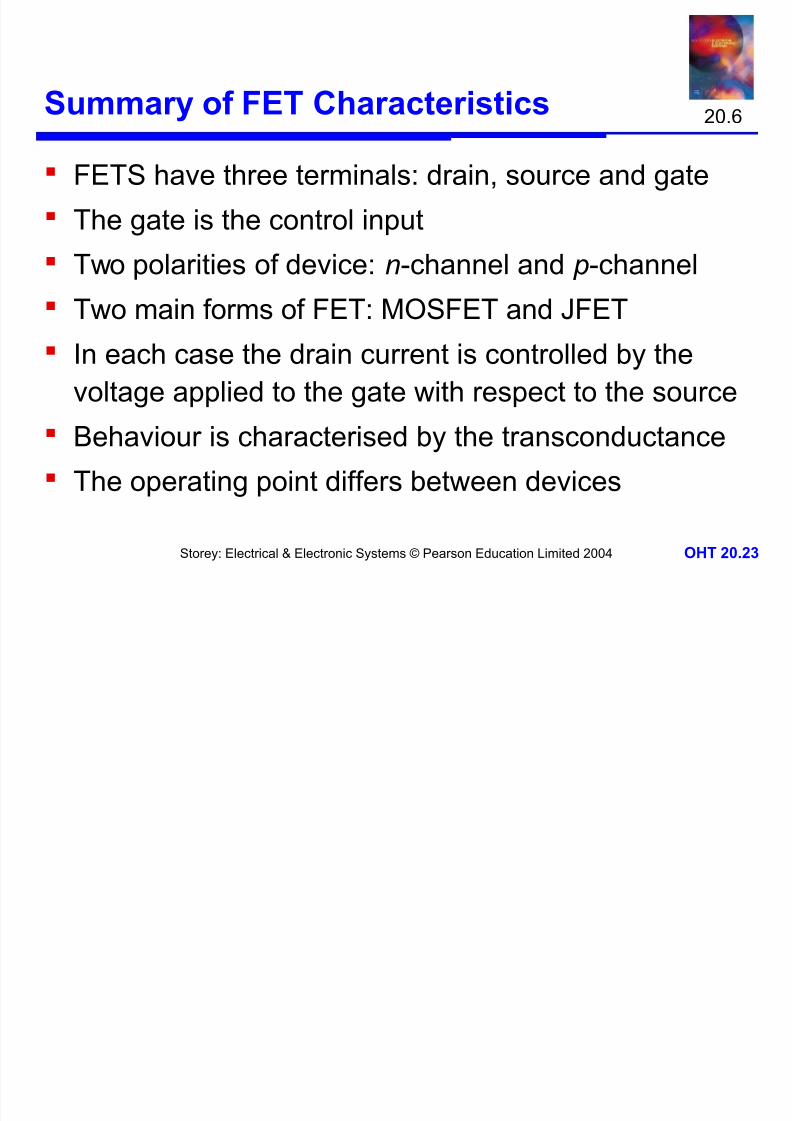
&u//ary of FET )'aracteristics
E"S ave tree terminals: drain. source and ,ate
"e ,ate is te control in'ut
"wo 'olarities of device: n!cannel and p!cannel "wo main forms of E": 1OSE" and $E"
In eac case te drain current is controlled *y te
volta,e a''lied to te ,ate wit res'ect to te source
?eaviour is caracterised *y te transconductance
"e o'eratin, 'oint differs *etween devices
20/@

7/25/2019 juction field transistor
http://slidepdf.com/reader/full/juction-field-transistor 24/32
Storey: Electrical & Electronic Systems © Pearson Education Limited 2004 OHT 20.2!
FET circuit
sy/ols4

7/25/2019 juction field transistor
http://slidepdf.com/reader/full/juction-field-transistor 25/32
Storey: Electrical & Electronic Systems © Pearson Education Limited 2004 OHT 20.2#
FET A/+lifiers
A si/+le E %O&FET a/+lifier
+ R G is used to 3ias te
,ate at its correct o'eratin,
'oint (wic for a7E 1OSE" is 0 )
+ C is a cou+ling ca+acitor
and is used to cou'le te
A% si,nal wile 'reventin,e6ternals circuits from
affectin, te *ias
+ tis is an A)-cou+led a/+lifier
20/B

7/25/2019 juction field transistor
http://slidepdf.com/reader/full/juction-field-transistor 26/32
Storey: Electrical & Electronic Systems © Pearson Education Limited 2004 OHT 20.2(
A)-cou+led a/+lifier
+ in'ut resistance + e;ual to R G
+ out'ut resistance + a''ro6imately e;ual to R D
+ ,ain + a''ro6imately +g mR D (te minus si,n sows tattis is an invertin, am'lifier)
+ C 'roduced a low!fre;uency cut!off at a fre;uency f c,iven *y
were R is te in'ut resistance of te am'lifier (wic intis case is e;ual to R G)
CR c
π 2
0= f

7/25/2019 juction field transistor
http://slidepdf.com/reader/full/juction-field-transistor 27/32
Storey: Electrical & Electronic Systems © Pearson Education Limited 2004 OHT 20.2*
"egative feedac5 a/+lifier
+ reduces 'ro*lems of varia*ility
of active com'onents
+ volta,e across R s is'ro'ortional to drain current.
wic is directly 'ro'ortional
to te out'ut volta,e
+ tis volta,e is su*tractedfrom in'ut volta,e to ,ate
+ ence negative feedac5

7/25/2019 juction field transistor
http://slidepdf.com/reader/full/juction-field-transistor 28/32
Storey: Electrical & Electronic Systems © Pearson Education Limited 2004 OHT 20.2,
&ource folloer
+ similar to earlier circuit.
*ut out'ut is now taen
from te source + feed*ac causes te
source to follow te in'ut
volta,e
+ 'roduces a unity-gaina/+lifier
+ also called a source folloer

7/25/2019 juction field transistor
http://slidepdf.com/reader/full/juction-field-transistor 29/32
Storey: Electrical & Electronic Systems © Pearson Education Limited 2004 OHT 20.2
Ot'er FET A++lications
A voltage controlled attenuator
+ for small drain!to!source
volta,es E"s resem*le
voltage-controlled resistors
+ te ,ate volta,e V G is used
to control tis resistance and
ence te ,ain of te 'otential
divider
+ used. for e6am'le. in auto/atic
gain control in radio receivers
20/C
7/25/2019 juction field transistor
http://slidepdf.com/reader/full/juction-field-transistor 30/32
Storey: Electrical & Electronic Systems © Pearson Education Limited 2004 OHT 20.30
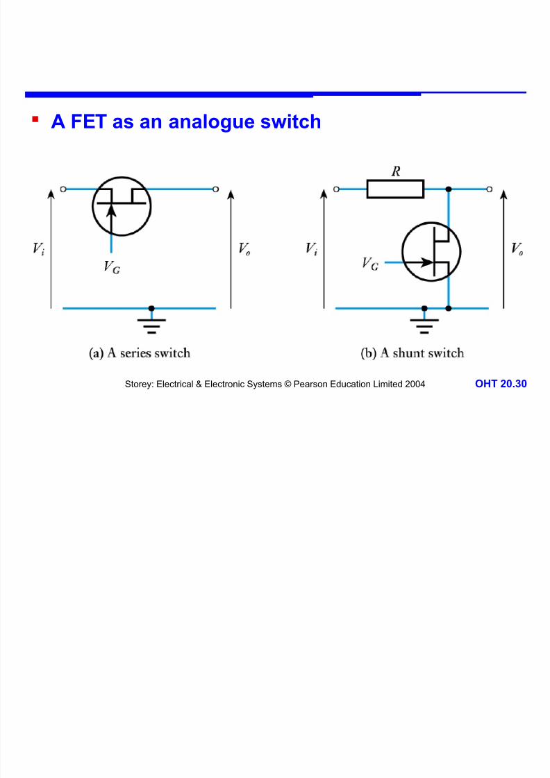
A FET as an analogue sitc'

7/25/2019 juction field transistor
http://slidepdf.com/reader/full/juction-field-transistor 31/32
Storey: Electrical & Electronic Systems © Pearson Education Limited 2004 OHT 20.31
A FET as a logical sitc'

7/25/2019 juction field transistor
http://slidepdf.com/reader/full/juction-field-transistor 32/32
Storey: Electrical & Electronic Systems © Pearson Education Limited 2004 OHT 20 32
6ey 7oints
E"s are widely used in *ot analo,ue and di,ital circuits
"ey ave i, in'ut resistance and small 'ysical si-e
"ere are two *asic forms of E": 1OSE"s and $E"s
1OSE"s may *e divided into 7E and Enancement ty'es
In eac case te ,ate volta,e controls te current from tedrain to te source
"e caracteristics of te various forms of E" are similar
e6ce't tat tey re;uire different *ias volta,es "e use of cou'lin, ca'acitors 'revents te am'lification of
7% and 'roduced A% am'lifiers
E"s can *e used to 'roduce various forms of am'lifier anda ran,e of oter circuit a''lications