Embed Size (px)
Citation preview
J O U R N A L O F M A T E R I A L S S C I E N C E 4 0 (2 0 0 5 ) 1 – 26
Review
Nano and macro-structured component
fabrication by electron beam-physical
vapor deposition (EB-PVD)
J. SINGH, D. E. WOLFEApplied Research Laboratory, The Pennsylvania State University, University Park, 115 MRIBuilding, PA 16804, USAE-mail: [email protected]
The objective of this paper is to demonstrate the versatility of electron beam-physical vapordeposition (EB-PVD) technology in engineering new materials with controlledmicrostructure and microchemistry in the form of coatings. EB-PVD technology is beingexplored in forming net-shaped components for many applications including space,turbine, optical, biomedical and auto industry. Coatings are often applied on componentsto extend their performance and life under severe environmental conditions includingthermal, corrosion, wear, and oxidation. In addition, coatings have been used in designingand developing sensors. Performance and properties of the coatings depend upon itscomposition, microstructure and deposition condition. This paper presents recent results ofvarious materials including ceramic, metallic, and functionally graded coatings producedby EB-PVD. Simultaneous co-evaporation of multiple ingots of different compositions in thehigh energy EB-PVD chamber has brought considerable interest in the architecture offunctional graded coatings, nano-laminated coatings and designing of new structuralmaterials that could not be produced economically by conventional methods. In addition,high evaporation and condensate rate allowed fabricating precision net-shapedcomponents with nanograined microstructure for various applications. This paper will alsopresent the results of various metallic and ceramic coatings including chromium, titaniumcarbide (TiC), hafnium carbide (HfC), tantalum carbide (TaC), hafnium nitride (HfN),titanium-boron-carbonitride (TiBCN), and partially yttria stabilized zirconia (YSZ), andHfO2-based TBC coatings deposited by EB-PVD for various applications. C© 2005 SpringerScience + Business Media, Inc.
1. IntroductionCoatings play an important role ranging from under-seato space applications including communications, sen-sors, satellites, optics, auto, and aerospace industries[1–6]. High temperature components of gas-turbineengines for aircraft such as airfoils and vanes arecoated with metallic and ceramic coatings to enhanceperformance and reliability [7–10]. Thus, there is acontinuous effort to engineer surface properties ofthe material enhancing the life of components undersevere environmental conditions where corrosion, high-temperature oxidation, and wear are concerns. Simi-larly, multilayered ceramic and metallic films are ex-tensively used in the fabrication of microelectronic andcommunication components [11, 12]. It is important tounderstand the inter-relationship of applications, coat-ings and processes. Applications dictate the selectionof coating materials, and the desired thermal, chemical,and mechanical properties often determine the deposi-tion method and processing parameters [13].
Coating process can be broadly classified into threegroups: vapor phase, which includes physical vapor de-position (PVD) and chemical vapor deposition (CVD);liquid phase, which-includes painting, dipping andelectroplating; and solid phase which includes plasmaspray processes and laser cladding [14–20]. Each pro-cess can again be sub-classified based on the source ofenergy used for the deposition of coatings as shown inTable I, and briefly discussed in the Appendix. Each ofthese processes has its advantages and disadvantages.Comparison of CVD, PVD and plasma spray processesis given in Table II [21–23]. Chemical and physical con-ditions during the deposition reaction can strongly af-fect the composition, residual stresses, and microstruc-ture (i.e., amorphous, polycrystalline, epitaxial, andtextured) of the coating. The desired coating thick-ness and material properties (including microstructure,physical, and mechanical properties) are dictated by itsapplication, which will determine the coating deposi-tion process to be used. The objective of this research
0022–2461 C© 2005 Springer Science + Business Media, Inc. 1
T ABL E I Coating deposition techniques [14–20]
Powder Spray deposition processes• Thermal spray, Plasma spray• High-velocity-oxy-fuel (HVOF)• Detonation gun (D-gun)
Chemical vapor deposition processes (CVD)• Low pressure CVD• Plasma enhanced CVD• Photochemical and laser-CVD
Physical vapor deposition processes (PVD)• Thermal evaporation• Electron beam-PVD• Sputtering
• Balanced and unbalanced magnetron sputtering• Direct current diode sputtering• Radio frequency sputtering• Triode-assisted PVD
• Cathodic arc• Ion plating
paper is to briefly review vapor phase coating growthmechanism followed by the most recent research workconducted in developing coatings/components for var-ious applications by the electron beam-physical vapordeposition (EB-PVD) process. In addition, the usageof EB-PVD technology will demonstrate in produc-ing near net-shaped components with controlled mi-crostructure and chemistry.
2. Electron beam-physical vapor deposition(EB-PVD) process
EB-PVD is a simple process in which a focused high-energy electron beam is directed to melt the evaporantmaterial(s) in a vacuum chamber (Fig. 1). The evap-orating material condenses on the surface of the sub-strates or components resulting in the formation of de-posit, i.e., coating. During deposition, external heating
T ABL E I I Comparison between CVD, PVD, EB-PVD and plasma spray processes [21–23]
Coating Substrate Deposition Surface Type of Typical Coatingprocess temperature (◦C) rate roughness bonding microstructure material Environment Flexibility
Plasma spray RT to 800 (flexible) >100 µm/min Very rough Mechanical Deformed-lamella Metal, ceramic Noise FlexibleCVD >800–1200 (must) <0.08 µm/min Smooth Diffusional Columnar, Metal, ceramic Chemical Limited
(<5 µm/h) Equiaxed gas disposalPVD- <600 (flexible) <0.08 µm/min Smooth Diffusional Columnar Metal, ceramic Clean Limited
sputtering (<5 µm/h)EB-PVD RT to 1200 .01 to 100 µm/min Smooth Diffusional Columnar, Metal, ceramic Clean Flexible
(flexible) nanograinedequiaxed
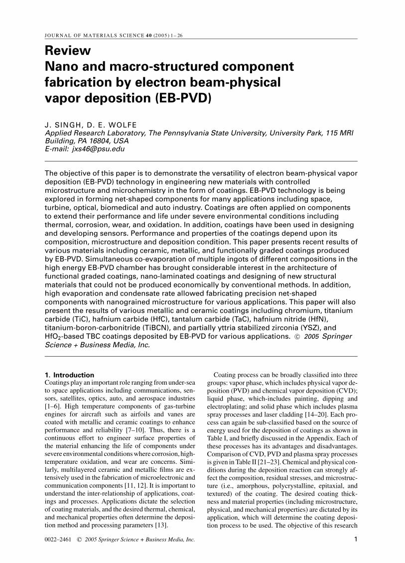
Figure 1 Schematic diagram showing: (a) straight and (b) electromagnetic deflected electron beam guns [24].
is often applied to the substrate for enhancing metal-lurgical bonding between the coating and the substrate.EB-PVD is primarily a line-of-sight process, therefore,uniform coating of complex parts (such as turbine air-foils) is accomplished by continuous rotation in the va-por cloud during the deposition process.
There are four main components in the EB-PVD unit,namely, EB-gun assembly, water cooled copper cru-cible which contains the material to be evaporated, thesubstrate (part to be coated), and the vacuum cham-ber unit with enhanced flexibility for a variety of coat-ing applications. The EB gun can be self-acceleratedstraight or electromagnetic deflected through 180 or270◦ as shown in Fig. 1. Similarly, the evaporant mate-rial is placed in a water-cooled copper crucible, whichcould be either pocket type for small quantity evapo-ration application (Fig. 1) or continuous ingot feedingthrough a copper-cooled crucible (Fig. 2 as marked A,B and C) for larger quantity evaporation. Flexibilityin the application of EB-PVD unit can be enhancedby using many EB guns and continuous multiple in-gots feeding system (Fig. 2) as discussed in the nextsection.
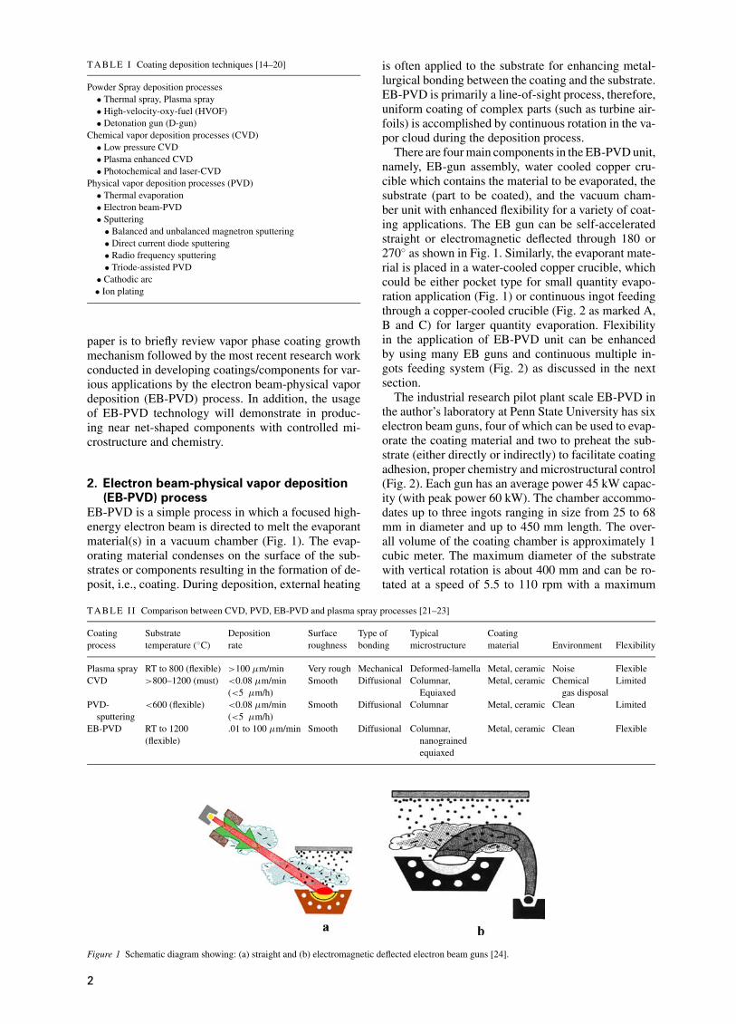
The industrial research pilot plant scale EB-PVD inthe author’s laboratory at Penn State University has sixelectron beam guns, four of which can be used to evap-orate the coating material and two to preheat the sub-strate (either directly or indirectly) to facilitate coatingadhesion, proper chemistry and microstructural control(Fig. 2). Each gun has an average power 45 kW capac-ity (with peak power 60 kW). The chamber accommo-dates up to three ingots ranging in size from 25 to 68mm in diameter and up to 450 mm length. The over-all volume of the coating chamber is approximately 1cubic meter. The maximum diameter of the substratewith vertical rotation is about 400 mm and can be ro-tated at a speed of 5.5 to 110 rpm with a maximum
2
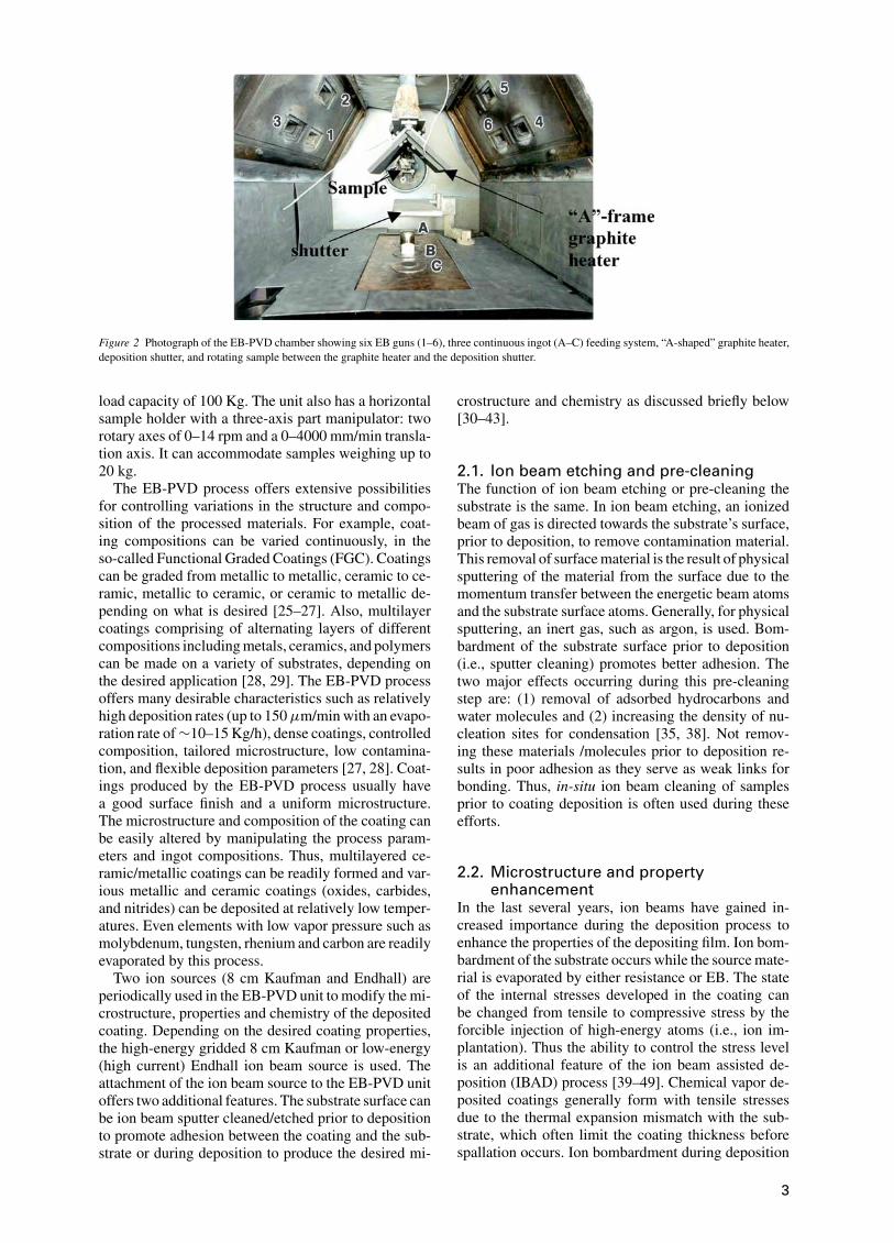
Figure 2 Photograph of the EB-PVD chamber showing six EB guns (1–6), three continuous ingot (A–C) feeding system, “A-shaped” graphite heater,deposition shutter, and rotating sample between the graphite heater and the deposition shutter.
load capacity of 100 Kg. The unit also has a horizontalsample holder with a three-axis part manipulator: tworotary axes of 0–14 rpm and a 0–4000 mm/min transla-tion axis. It can accommodate samples weighing up to20 kg.
The EB-PVD process offers extensive possibilitiesfor controlling variations in the structure and compo-sition of the processed materials. For example, coat-ing compositions can be varied continuously, in theso-called Functional Graded Coatings (FGC). Coatingscan be graded from metallic to metallic, ceramic to ce-ramic, metallic to ceramic, or ceramic to metallic de-pending on what is desired [25–27]. Also, multilayercoatings comprising of alternating layers of differentcompositions including metals, ceramics, and polymerscan be made on a variety of substrates, depending onthe desired application [28, 29]. The EB-PVD processoffers many desirable characteristics such as relativelyhigh deposition rates (up to 150 µm/min with an evapo-ration rate of ∼10–15 Kg/h), dense coatings, controlledcomposition, tailored microstructure, low contamina-tion, and flexible deposition parameters [27, 28]. Coat-ings produced by the EB-PVD process usually havea good surface finish and a uniform microstructure.The microstructure and composition of the coating canbe easily altered by manipulating the process param-eters and ingot compositions. Thus, multilayered ce-ramic/metallic coatings can be readily formed and var-ious metallic and ceramic coatings (oxides, carbides,and nitrides) can be deposited at relatively low temper-atures. Even elements with low vapor pressure such asmolybdenum, tungsten, rhenium and carbon are readilyevaporated by this process.
Two ion sources (8 cm Kaufman and Endhall) areperiodically used in the EB-PVD unit to modify the mi-crostructure, properties and chemistry of the depositedcoating. Depending on the desired coating properties,the high-energy gridded 8 cm Kaufman or low-energy(high current) Endhall ion beam source is used. Theattachment of the ion beam source to the EB-PVD unitoffers two additional features. The substrate surface canbe ion beam sputter cleaned/etched prior to depositionto promote adhesion between the coating and the sub-strate or during deposition to produce the desired mi-
crostructure and chemistry as discussed briefly below[30–43].
2.1. Ion beam etching and pre-cleaningThe function of ion beam etching or pre-cleaning thesubstrate is the same. In ion beam etching, an ionizedbeam of gas is directed towards the substrate’s surface,prior to deposition, to remove contamination material.This removal of surface material is the result of physicalsputtering of the material from the surface due to themomentum transfer between the energetic beam atomsand the substrate surface atoms. Generally, for physicalsputtering, an inert gas, such as argon, is used. Bom-bardment of the substrate surface prior to deposition(i.e., sputter cleaning) promotes better adhesion. Thetwo major effects occurring during this pre-cleaningstep are: (1) removal of adsorbed hydrocarbons andwater molecules and (2) increasing the density of nu-cleation sites for condensation [35, 38]. Not remov-ing these materials /molecules prior to deposition re-sults in poor adhesion as they serve as weak links forbonding. Thus, in-situ ion beam cleaning of samplesprior to coating deposition is often used during theseefforts.
2.2. Microstructure and propertyenhancement
In the last several years, ion beams have gained in-creased importance during the deposition process toenhance the properties of the depositing film. Ion bom-bardment of the substrate occurs while the source mate-rial is evaporated by either resistance or EB. The stateof the internal stresses developed in the coating canbe changed from tensile to compressive stress by theforcible injection of high-energy atoms (i.e., ion im-plantation). Thus the ability to control the stress levelis an additional feature of the ion beam assisted de-position (IBAD) process [39–49]. Chemical vapor de-posited coatings generally form with tensile stressesdue to the thermal expansion mismatch with the sub-strate, which often limit the coating thickness beforespallation occurs. Ion bombardment during deposition
3
has a tendency to reduce the tensile stress and oftenchanges the intrinsic stress from tensile to compressive[41–49]. Depending on the energy of the ion beam,texturing or preferred crystal growth orientation can becontrolled [50–60]. IBAD can be used to change opti-cal properties and decrease the permeability of water byincreasing the density of the deposited film. Changesin the crystal structure of the film have also been re-ported with IBAD. For example, the microstructure ofZrO2 has been changed from amorphous to polycrys-talline using IBAD [61]. In addition, the morphology ofmolybdenum films deposited on silicon were shown tochange from columnar to isotropic due to ion bombard-ment [44]. In addition, numerous authors have reportedincreases in the average hardness of coatings depositedwith IBAD [38, 62–66]. The increase in hardness isobtained by increasing the density, decreasing grainsize, changing stress state, and controlling the crystallo-graphic texture of the coating. Improved step coverage(i.e., high surface roughness or complex geometries)has also been reported when using IBAD [67]. This ismost likely the result of increased atom mobility underbombardment.
In addition, ion beams are used in synthesizing coat-ings by reacting the evaporant with the ionized reactivegases including nitrogen, oxygen, methane and acety-lene. Ionized gas chemically reacts with the vapor cloudforming alloyed coatings such as nitrides of Hf, Ti, Zr;carbides of Ti, Hf, Ta, and Zr, and oxides of Zr andAl.
The choice of the deposition technique is determinedby the application for the coating, the desired coatingproperties, temperature limitation of the substrate, uni-formity or consistency of the process, and its compati-bility with subsequent processing steps. Chemical andphysical conditions during the deposition reaction canstrongly affect the resultant microstructure of the coat-ing (i.e., single-crystalline, polycrystalline, amorphous,epitaxial). Multilayered metallic or ceramic coatingsare often applied on the components to achieve thedesired properties. Properties and performance of thecoating are heavily dependent upon the coating mi-crostructure. It has been well established that multi-layered coatings with the layer thickness of <1 µmoffer superior structural and physical properties dueto refined microstructure in the coating [68–70]. Inall vapor-phase coating processes including CVD andPVD, the basic mechanisms of coating growth are verysimilar, therefore it is important to briefly review thinfilm growth mechanisms.
3. Nucleation and growth mechanismsof thin films
The films growth mechanism remains the same as de-posited by either CVD or PVD including sputteringand EB-PVD. Significant progress has been made inunderstanding the nucleation and growth mechanismof thin films [71–73]. The structural evolution of thinfilm undergoes three main stages:
(i) In the early stage, vapor will condense on thesubstrate and migrate to a site where lowest activation
Figure 3 Schematic diagram illustrating nucleation and growth se-quence of thin films [44].
energy is available for the nucleation to occur. It iscalled the nucleation stage (Fig. 3a).
(ii) Next step is the incorporation of incoming con-densation flux into the growing individual units of thefilm structure. The condensate will try to re-structurein order to reduce surface free energy (ϒ). This step iscalled a crystal/film growth. Since the surface free en-ergy is generally an anisotropic property, crystal growthwill take place initially in all directions to reduce thesurface free energy (it will follow the stages as shownin Fig. 3b and c).
(iii) Re-organize the unit structure of the film. It iscalled grain growth by coalescence (as shown in Fig. 3dand e). This depends upon the substrate depositiontemperature, or total energy of the system.
It is evident from Fig. 3 that the final structure of thefilm is a result of the creation of multiple nucleationevents followed by subsequent growth of the structuralunits (grains in crystalline materials) and their peri-odic reorganization during coalescence. The continu-ous growth and coalescence process is associated withthe surface free energy, surface diffusion and bulk dif-fusion that are dependent upon the substrate deposi-tion temperature and total energy of the system. Dur-ing the growth process, individual grains grow in theform of single crystals. Microstructural evolution ofthe thick films and bulk coatings have been investi-gated as a function of melting point of coating mate-rials (TMP), substrate temperature (Tsub), and pressureduring the deposition and is summarized by the wellknown structure zone models as shown in Fig. 4a [74–78]. Zone 1 consists of dome topped, tapered crystalsseparated by voids and such microstructure is observedat homologous temperature Tsub/TMP < 0.3 and is dueto insufficient surface diffusion of adatoms. Transitionzone or Zone T (ZT) microstructures generally occurin energy-enhanced deposition processes (i.e., IBADand higher temperature). The additional energy in-creases atom mobility resulting in fewer voids betweenthe discontinuous columns observed in Z1 microstruc-ture. ZT structure is often densely packed fibrousgrains. Zone 2 (Z2)consists of dense columnar grainswith a smooth, sometimes faceted surface, resultingfrom surface dominant condensation and is observed at
4
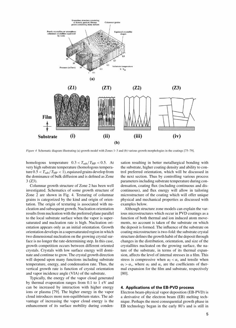
Figure 4 Schematic diagram illustrating (a) growth model with Zones 1–3 and (b) various growth morphologies in the coatings [75–79].
homologous temperature 0.3 < Tsub/TMP < 0.5. Atvery high substrate temperature (homologous tempera-ture 0.5 < Tsub/TMP < 1), equiaxed grains develop fromthe dominance of bulk diffusion and is defined as Zone3 (Z3).
Columnar growth structure of Zone 2 has been wellinvestigated. Schematics of some growth structure ofZone 2 are shown in Fig. 4. Texturing of columnargrains is categorized by the kind and origin of orien-tation. The origin of texturing is associated with nu-cleation and subsequent growth. Nucleation orientationresults from nucleation with the preferred plane parallelto the local substrate surface when the vapor is super-saturated and nucleation rate is high. Nucleation ori-entation appears only as an initial orientation. Growthorientation develops in a supersaturated region in whichtwo dimensional nucleation on the growing crystal sur-face is no longer the rate-determining step. In this case,growth competition occurs between different orientedcrystals. Crystals with low surface energy will domi-nate and continue to grow. The crystal growth directionwill depend upon many functions including substratetemperature, energy, and condensation rate. Thus, thevertical growth rate is function of crystal orientationand vapor incidence angle (VIA) of the substrate.
Typically, the energy of the vapor cloud generatedby thermal evaporation ranges from 0.1 to 1 eV andcan be increased by interaction with higher energyions or plasma [79]. The higher energy in the vaporcloud introduces more non-equilibrium states. The ad-vantage of increasing the vapor cloud energy is theenhancement of its surface mobility during conden-
sation resulting in better metallurgical bonding withthe substrate, higher coating density and ability to con-trol preferred orientation, which will be discussed inthe next section. Thus by controlling various processparameters including substrate temperature during con-densation, coating flux (including continuous and dis-continuous), and flux energy will allow in tailoringmicrostructure of the coating which will offer uniquephysical and mechanical properties as discussed withexamples below.
Although structure zone models can explain the var-ious microstructures which occur in PVD coatings as afunction of both thermal and ion induced atom move-ments, no account is taken of the substrate on whichthe deposit is formed. The influence of the substrate oncoating microstructure is two-fold: the substrate crystalstructure defines the growth habit of the deposit throughchanges in the distribution, orientation, and size of thecrystallites nucleated on the growing surface, the na-ture of the substrate, in terms of its thermal expan-sion, affects the level of internal stresses in a film. Thisstress is compressive when αf < αs and tensile whenαf > αs, where αf and αs are the coefficients of ther-mal expansion for the film and substrate, respectively[80].
4. Applications of the EB-PVD processElectron beam-physical vapor deposition (EB-PVD) isa derivative of the electron beam (EB) melting tech-nique. Perhaps the most consequential growth phase inEB technology began in the early 80’s and is still in
5
progress. This significant progress was driven by threefactors: (i) greatly improved vacuum generation tech-nology, (ii) significant advancement in computers, and(iii) availability of high quality EB-guns. Since then,EB technology has been developed for a wide rangeof applications including surface treatment, welding,glazing and evaporation for coatings. Incorporation ofan ion source in the EB-PVD chamber with multipleingots has increased its versatility in developing newmaterials with a very wide range of applications such asmicro-electronics, sensors, optics, aerospace and bio-medical industries. Some successful applications of theEB-PVD and ion beam-assisted EB-PVD processes aregiven below.
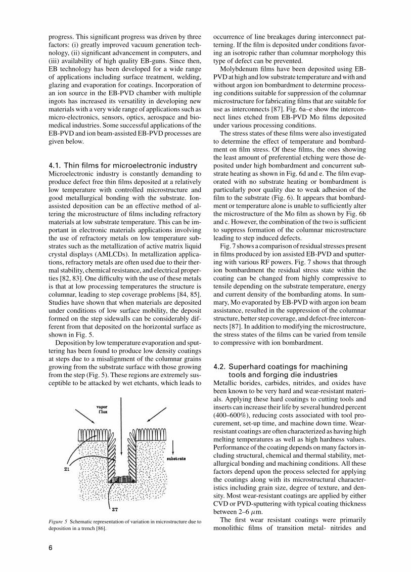
4.1. Thin films for microelectronic industryMicroelectronic industry is constantly demanding toproduce defect free thin films deposited at a relativelylow temperature with controlled microstructure andgood metallurgical bonding with the substrate. Ion-assisted deposition can be an effective method of al-tering the microstructure of films including refractorymaterials at low substrate temperature. This can be im-portant in electronic materials applications involvingthe use of refractory metals on low temperature sub-strates such as the metallization of active matrix liquidcrystal displays (AMLCDs). In metallization applica-tions, refractory metals are often used due to their ther-mal stability, chemical resistance, and electrical proper-ties [82, 83]. One difficulty with the use of these metalsis that at low processing temperatures the structure iscolumnar, leading to step coverage problems [84, 85].Studies have shown that when materials are depositedunder conditions of low surface mobility, the depositformed on the step sidewalls can be considerably dif-ferent from that deposited on the horizontal surface asshown in Fig. 5.
Deposition by low temperature evaporation and sput-tering has been found to produce low density coatingsat steps due to a misalignment of the columnar grainsgrowing from the substrate surface with those growingfrom the step (Fig. 5). These regions are extremely sus-ceptible to be attacked by wet etchants, which leads to
Figure 5 Schematic representation of variation in microstructure due todeposition in a trench [86].
occurrence of line breakages during interconnect pat-terning. If the film is deposited under conditions favor-ing an isotropic rather than columnar morphology thistype of defect can be prevented.
Molybdenum films have been deposited using EB-PVD at high and low substrate temperature and with andwithout argon ion bombardment to determine process-ing conditions suitable for suppression of the columnarmicrostructure for fabricating films that are suitable foruse as interconnects [87]. Fig. 6a–e show the intercon-nect lines etched from EB-PVD Mo films depositedunder various processing conditions.
The stress states of these films were also investigatedto determine the effect of temperature and bombard-ment on film stress. Of these films, the ones showingthe least amount of preferential etching were those de-posited under high bombardment and concurrent sub-strate heating as shown in Fig. 6d and e. The film evap-orated with no substrate heating or bombardment isparticularly poor quality due to weak adhesion of thefilm to the substrate (Fig. 6). It appears that bombard-ment or temperature alone is unable to sufficiently alterthe microstructure of the Mo film as shown by Fig. 6band c. However, the combination of the two is sufficientto suppress formation of the columnar microstructureleading to step induced defects.
Fig. 7 shows a comparison of residual stresses presentin films produced by ion assisted EB-PVD and sputter-ing with various RF powers. Fig. 7 shows that throughion bombardment the residual stress state within thecoating can be changed from highly compressive totensile depending on the substrate temperature, energyand current density of the bombarding atoms. In sum-mary, Mo evaporated by EB-PVD with argon ion beamassistance, resulted in the suppression of the columnarstructure, better step coverage, and defect-free intercon-nects [87]. In addition to modifying the microstructure,the stress states of the films can be varied from tensileto compressive with ion bombardment.
4.2. Superhard coatings for machiningtools and forging die industries
Metallic borides, carbides, nitrides, and oxides havebeen known to be very hard and wear-resistant materi-als. Applying these hard coatings to cutting tools andinserts can increase their life by several hundred percent(400–600%), reducing costs associated with tool pro-curement, set-up time, and machine down time. Wear-resistant coatings are often characterized as having highmelting temperatures as well as high hardness values.Performance of the coating depends on many factors in-cluding structural, chemical and thermal stability, met-allurgical bonding and machining conditions. All thesefactors depend upon the process selected for applyingthe coatings along with its microstructural character-istics including grain size, degree of texture, and den-sity. Most wear-resistant coatings are applied by eitherCVD or PVD-sputtering with typical coating thicknessbetween 2–6 µm.
The first wear resistant coatings were primarilymonolithic films of transition metal- nitrides and
6
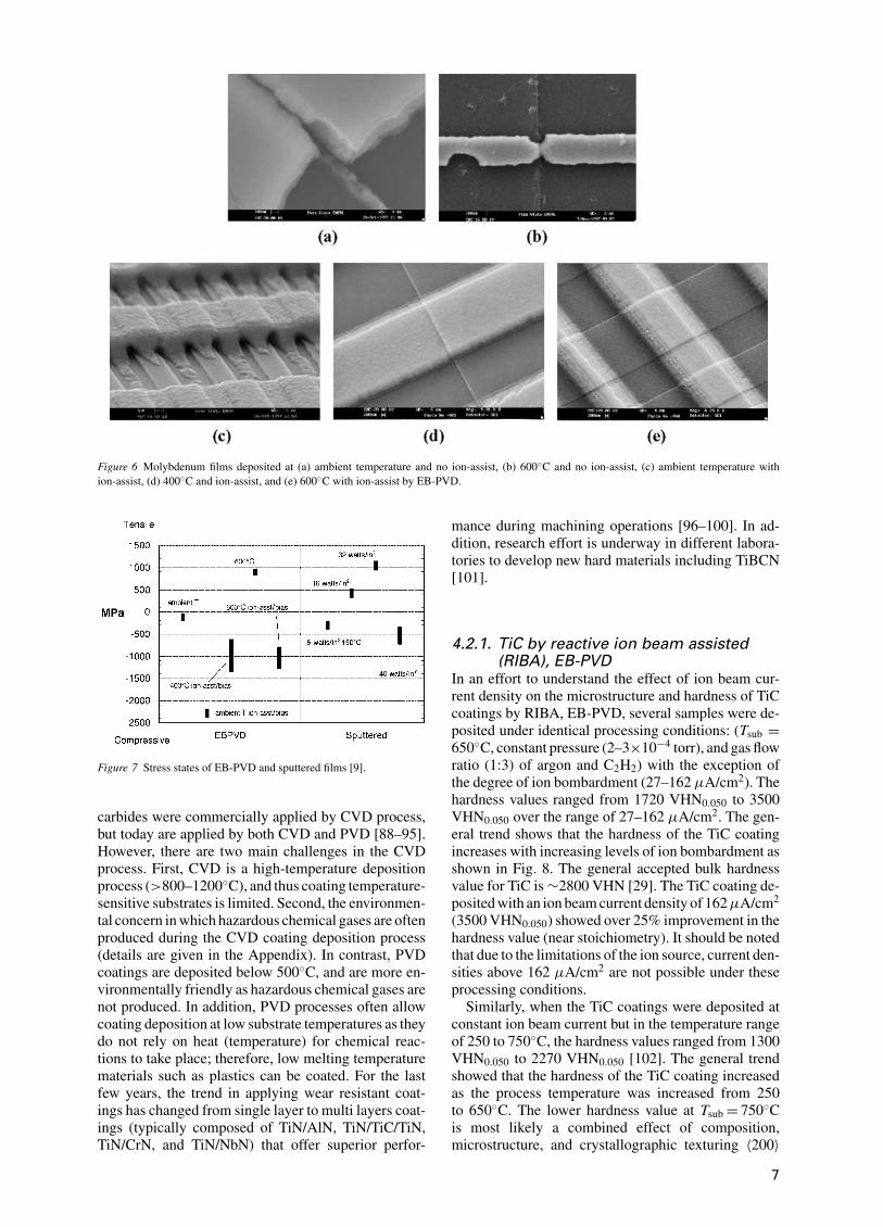
Figure 6 Molybdenum films deposited at (a) ambient temperature and no ion-assist, (b) 600◦C and no ion-assist, (c) ambient temperature withion-assist, (d) 400◦C and ion-assist, and (e) 600◦C with ion-assist by EB-PVD.
Figure 7 Stress states of EB-PVD and sputtered films [9].
carbides were commercially applied by CVD process,but today are applied by both CVD and PVD [88–95].However, there are two main challenges in the CVDprocess. First, CVD is a high-temperature depositionprocess (>800–1200◦C), and thus coating temperature-sensitive substrates is limited. Second, the environmen-tal concern in which hazardous chemical gases are oftenproduced during the CVD coating deposition process(details are given in the Appendix). In contrast, PVDcoatings are deposited below 500◦C, and are more en-vironmentally friendly as hazardous chemical gases arenot produced. In addition, PVD processes often allowcoating deposition at low substrate temperatures as theydo not rely on heat (temperature) for chemical reac-tions to take place; therefore, low melting temperaturematerials such as plastics can be coated. For the lastfew years, the trend in applying wear resistant coat-ings has changed from single layer to multi layers coat-ings (typically composed of TiN/AlN, TiN/TiC/TiN,TiN/CrN, and TiN/NbN) that offer superior perfor-
mance during machining operations [96–100]. In ad-dition, research effort is underway in different labora-tories to develop new hard materials including TiBCN[101].
4.2.1. TiC by reactive ion beam assisted(RIBA), EB-PVD
In an effort to understand the effect of ion beam cur-rent density on the microstructure and hardness of TiCcoatings by RIBA, EB-PVD, several samples were de-posited under identical processing conditions: (Tsub =650◦C, constant pressure (2–3×10⁻⁴ torr), and gas flowratio (1:3) of argon and C2H2) with the exception ofthe degree of ion bombardment (27–162 µA/cm2). Thehardness values ranged from 1720 VHN0.050 to 3500VHN0.050 over the range of 27–162 µA/cm2. The gen-eral trend shows that the hardness of the TiC coatingincreases with increasing levels of ion bombardment asshown in Fig. 8. The general accepted bulk hardnessvalue for TiC is ∼2800 VHN [29]. The TiC coating de-posited with an ion beam current density of 162µA/cm2
(3500 VHN0.050) showed over 25% improvement in thehardness value (near stoichiometry). It should be notedthat due to the limitations of the ion source, current den-sities above 162 µA/cm2 are not possible under theseprocessing conditions.
Similarly, when the TiC coatings were deposited atconstant ion beam current but in the temperature rangeof 250 to 750◦C, the hardness values ranged from 1300VHN0.050 to 2270 VHN0.050 [102]. The general trendshowed that the hardness of the TiC coating increasedas the process temperature was increased from 250to 650◦C. The lower hardness value at Tsub = 750◦Cis most likely a combined effect of composition,microstructure, and crystallographic texturing 〈200〉
7
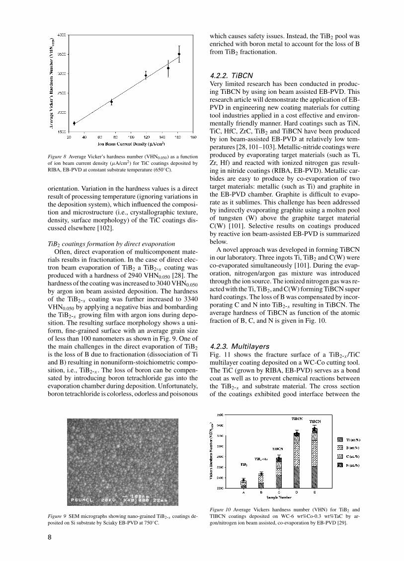
Figure 8 Average Vicker’s hardness number (VHN0.050) as a functionof ion beam current density (µA/cm2) for TiC coatings deposited byRIBA, EB-PVD at constant substrate temperature (650◦C).
orientation. Variation in the hardness values is a directresult of processing temperature (ignoring variations inthe deposition system), which influenced the composi-tion and microstructure (i.e., crystallographic texture,density, surface morphology) of the TiC coatings dis-cussed elsewhere [102].
TiB2 coatings formation by direct evaporationOften, direct evaporation of multicomponent mate-
rials results in fractionation. In the case of direct elec-tron beam evaporation of TiB2 a TiB2-x coating wasproduced with a hardness of 2940 VHN0.050 [28]. Thehardness of the coating was increased to 3040 VHN0.050by argon ion beam assisted deposition. The hardnessof the TiB2-x coating was further increased to 3340VHN0.050 by applying a negative bias and bombardingthe TiB2-x growing film with argon ions during depo-sition. The resulting surface morphology shows a uni-form, fine-grained surface with an average grain sizeof less than 100 nanometers as shown in Fig. 9. One ofthe main challenges in the direct evaporation of TiB2is the loss of B due to fractionation (dissociation of Tiand B) resulting in nonuniform-stoichiometric compo-sition, i.e., TiB2-x . The loss of boron can be compen-sated by introducing boron tetrachloride gas into theevaporation chamber during deposition. Unfortunately,boron tetrachloride is colorless, odorless and poisonous
Figure 9 SEM micrographs showing nano-grained TiB2-x coatings de-posited on Si substrate by Sciaky EB-PVD at 750◦C.
which causes safety issues. Instead, the TiB2 pool wasenriched with boron metal to account for the loss of Bfrom TiB2 fractionation.
4.2.2. TiBCNVery limited research has been conducted in produc-ing TiBCN by using ion beam assisted EB-PVD. Thisresearch article will demonstrate the application of EB-PVD in engineering new coating materials for cuttingtool industries applied in a cost effective and environ-mentally friendly manner. Hard coatings such as TiN,TiC, HfC, ZrC, TiB2 and TiBCN have been producedby ion beam-assisted EB-PVD at relatively low tem-peratures [28, 101–103]. Metallic-nitride coatings wereproduced by evaporating target materials (such as Ti,Zr, Hf) and reacted with ionized nitrogen gas result-ing in nitride coatings (RIBA, EB-PVD). Metallic car-bides are easy to produce by co-evaporation of twotarget materials: metallic (such as Ti) and graphite inthe EB-PVD chamber. Graphite is difficult to evapo-rate as it sublimes. This challenge has been addressedby indirectly evaporating graphite using a molten poolof tungsten (W) above the graphite target materialC(W) [101]. Selective results on coatings producedby reactive ion beam-assisted EB-PVD is summarizedbelow.
A novel approach was developed in forming TiBCNin our laboratory. Three ingots Ti, TiB2 and C(W) wereco-evaporated simultaneously [101]. During the evap-oration, nitrogen/argon gas mixture was introducedthrough the ion source. The ionized nitrogen gas was re-acted with the Ti, TiB2, and C(W) forming TiBCN superhard coatings. The loss of B was compensated by incor-porating C and N into TiB2-x resulting in TiBCN. Theaverage hardness of TiBCN as function of the atomicfraction of B, C, and N is given in Fig. 10.
4.2.3. MultilayersFig. 11 shows the fracture surface of a TiB2-x /TiCmultilayer coating deposited on a WC-Co cutting tool.The TiC (grown by RIBA, EB-PVD) serves as a bondcoat as well as to prevent chemical reactions betweenthe TiB2-x and substrate material. The cross sectionof the coatings exhibited good interface between the
Figure 10 Average Vickers hardness number (VHN) for TiB2 andTIBCN coatings deposited on WC-6 wt%Co-0.3 wt%TaC by ar-gon/nitrogen ion beam assisted, co-evaporation by EB-PVD [29].
8
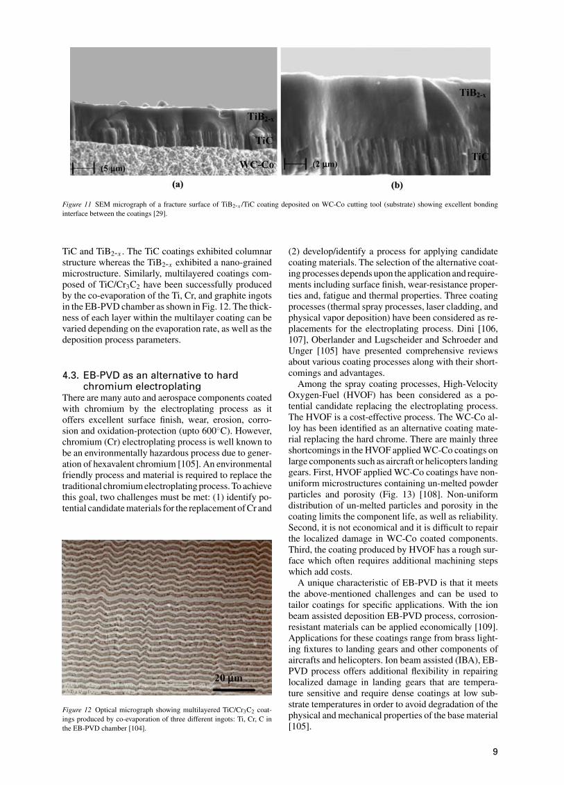
Figure 11 SEM micrograph of a fracture surface of TiB2-x /TiC coating deposited on WC-Co cutting tool (substrate) showing excellent bondinginterface between the coatings [29].
TiC and TiB2-x . The TiC coatings exhibited columnarstructure whereas the TiB2-x exhibited a nano-grainedmicrostructure. Similarly, multilayered coatings com-posed of TiC/Cr3C2 have been successfully producedby the co-evaporation of the Ti, Cr, and graphite ingotsin the EB-PVD chamber as shown in Fig. 12. The thick-ness of each layer within the multilayer coating can bevaried depending on the evaporation rate, as well as thedeposition process parameters.
4.3. EB-PVD as an alternative to hardchromium electroplating
There are many auto and aerospace components coatedwith chromium by the electroplating process as itoffers excellent surface finish, wear, erosion, corro-sion and oxidation-protection (upto 600◦C). However,chromium (Cr) electroplating process is well known tobe an environmentally hazardous process due to gener-ation of hexavalent chromium [105]. An environmentalfriendly process and material is required to replace thetraditional chromium electroplating process. To achievethis goal, two challenges must be met: (1) identify po-tential candidate materials for the replacement of Cr and
Figure 12 Optical micrograph showing multilayered TiC/Cr3C2 coat-ings produced by co-evaporation of three different ingots: Ti, Cr, C inthe EB-PVD chamber [104].
(2) develop/identify a process for applying candidatecoating materials. The selection of the alternative coat-ing processes depends upon the application and require-ments including surface finish, wear-resistance proper-ties and, fatigue and thermal properties. Three coatingprocesses (thermal spray processes, laser cladding, andphysical vapor deposition) have been considered as re-placements for the electroplating process. Dini [106,107], Oberlander and Lugscheider and Schroeder andUnger [105] have presented comprehensive reviewsabout various coating processes along with their short-comings and advantages.
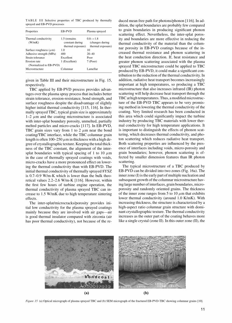
Among the spray coating processes, High-VelocityOxygen-Fuel (HVOF) has been considered as a po-tential candidate replacing the electroplating process.The HVOF is a cost-effective process. The WC-Co al-loy has been identified as an alternative coating mate-rial replacing the hard chrome. There are mainly threeshortcomings in the HVOF applied WC-Co coatings onlarge components such as aircraft or helicopters landinggears. First, HVOF applied WC-Co coatings have non-uniform microstructures containing un-melted powderparticles and porosity (Fig. 13) [108]. Non-uniformdistribution of un-melted particles and porosity in thecoating limits the component life, as well as reliability.Second, it is not economical and it is difficult to repairthe localized damage in WC-Co coated components.Third, the coating produced by HVOF has a rough sur-face which often requires additional machining stepswhich add costs.
A unique characteristic of EB-PVD is that it meetsthe above-mentioned challenges and can be used totailor coatings for specific applications. With the ionbeam assisted deposition EB-PVD process, corrosion-resistant materials can be applied economically [109].Applications for these coatings range from brass light-ing fixtures to landing gears and other components ofaircrafts and helicopters. Ion beam assisted (IBA), EB-PVD process offers additional flexibility in repairinglocalized damage in landing gears that are tempera-ture sensitive and require dense coatings at low sub-strate temperatures in order to avoid degradation of thephysical and mechanical properties of the base material[105].
9
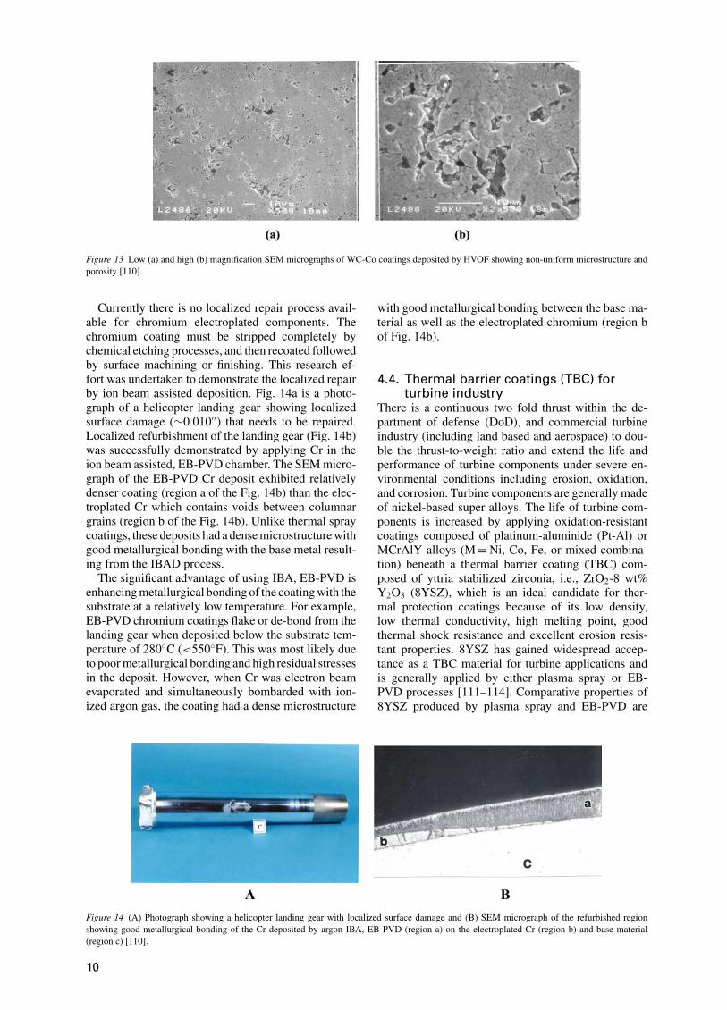
Figure 13 Low (a) and high (b) magnification SEM micrographs of WC-Co coatings deposited by HVOF showing non-uniform microstructure andporosity [110].
Currently there is no localized repair process avail-able for chromium electroplated components. Thechromium coating must be stripped completely bychemical etching processes, and then recoated followedby surface machining or finishing. This research ef-fort was undertaken to demonstrate the localized repairby ion beam assisted deposition. Fig. 14a is a photo-graph of a helicopter landing gear showing localizedsurface damage (∼0.010′′) that needs to be repaired.Localized refurbishment of the landing gear (Fig. 14b)was successfully demonstrated by applying Cr in theion beam assisted, EB-PVD chamber. The SEM micro-graph of the EB-PVD Cr deposit exhibited relativelydenser coating (region a of the Fig. 14b) than the elec-troplated Cr which contains voids between columnargrains (region b of the Fig. 14b). Unlike thermal spraycoatings, these deposits had a dense microstructure withgood metallurgical bonding with the base metal result-ing from the IBAD process.
The significant advantage of using IBA, EB-PVD isenhancing metallurgical bonding of the coating with thesubstrate at a relatively low temperature. For example,EB-PVD chromium coatings flake or de-bond from thelanding gear when deposited below the substrate tem-perature of 280◦C (<550◦F). This was most likely dueto poor metallurgical bonding and high residual stressesin the deposit. However, when Cr was electron beamevaporated and simultaneously bombarded with ion-ized argon gas, the coating had a dense microstructure
Figure 14 (A) Photograph showing a helicopter landing gear with localized surface damage and (B) SEM micrograph of the refurbished regionshowing good metallurgical bonding of the Cr deposited by argon IBA, EB-PVD (region a) on the electroplated Cr (region b) and base material(region c) [110].
with good metallurgical bonding between the base ma-terial as well as the electroplated chromium (region bof Fig. 14b).
4.4. Thermal barrier coatings (TBC) forturbine industry
There is a continuous two fold thrust within the de-partment of defense (DoD), and commercial turbineindustry (including land based and aerospace) to dou-ble the thrust-to-weight ratio and extend the life andperformance of turbine components under severe en-vironmental conditions including erosion, oxidation,and corrosion. Turbine components are generally madeof nickel-based super alloys. The life of turbine com-ponents is increased by applying oxidation-resistantcoatings composed of platinum-aluminide (Pt-Al) orMCrAlY alloys (M = Ni, Co, Fe, or mixed combina-tion) beneath a thermal barrier coating (TBC) com-posed of yttria stabilized zirconia, i.e., ZrO2-8 wt%Y2O3 (8YSZ), which is an ideal candidate for ther-mal protection coatings because of its low density,low thermal conductivity, high melting point, goodthermal shock resistance and excellent erosion resis-tant properties. 8YSZ has gained widespread accep-tance as a TBC material for turbine applications andis generally applied by either plasma spray or EB-PVD processes [111–114]. Comparative properties of8YSZ produced by plasma spray and EB-PVD are
10
T ABL E I I I Selective properties of TBC produced by thermallysprayed and EB-PVD processes
Properties EB-PVD Plasma sprayed
Thermal conductivity 1.5 (remains 0.8–>1.8(W/mK) constant during (changes during
thermal exposure) thermal exposure)Surface roughness (µm) 1.0 10Adhesive strength (MPa) 400 20–40Strain tolerance Excellent PoorErosion rate 1 (Excellent) 7 (Poor)
(Normalized to EB-PVD)Microstructure Columnar Lamellar
given in Table III and their microstructure in Fig. 15,respectively.
TBC applied by EB-PVD process provides advan-tages over the plasma spray process that includes betterstrain tolerance, erosion-resistance, bond strength, andsurface roughness despite the disadvantage of slightlyhigher initial thermal conductivity [115, 116]. In ther-mally sprayed TBC, typical grain size is approximately1–2 µm and the coating microstructure is associatedwith inter-splat boundary porosity, unmelted, partiallymelted particles and micro-cracks [117]. In EB-PVD,TBC grain sizes vary from 1 to 2 µm near the bondcoating/TBC interface, while the TBC columnar grainlength is often 100–250 µm in thickness with a high de-gree of crystallographic texture. Keeping the total thick-ness of the TBC constant, the alignment of the inter-splat boundaries with typical spacing of 1 to 10 µmin the case of thermally sprayed coatings with voids,micro-cracks have a more pronounced effect on lower-ing the thermal conductivity than with EB-PVD. Theinitial thermal conductivity of thermally sprayed 8YSZis 0.7–0.9 W/m-K which is lower than the bulk theo-retical values 2.2–2.6 W/m-K [116]. However, withinthe first few hours of turbine engine operation, thethermal conductivity of plasma sprayed TBC can in-crease to 1.5 W/mK due to high temperature sinteringeffects.
The inter-splat/microcracks/porosity provides ini-tial low conductivity for the plasma sprayed coatingsmainly because they are involved with air gaps—airis good thermal insulator compared with zirconia (airhas poor thermal conductivity), not because of the re-
Figure 15 (a) Optical micrograph of plasma sprayed TBC and (b) SEM micrograph of the fractured EB-PVD-TBC showing columnar grains [10].
duced mean free path for photons/phonon [116]. In ad-dition, the splat boundaries are probably few comparedto grain boundaries in producing significant phononscattering effect. Nevertheless, the inter-splat poros-ity and boundaries are more effective in reducing thethermal conductivity of the material than the colum-nar porosity in EB-PVD coatings because of the in-creased thermal resistance and phonon scattering inthe heat conduction direction. If, heat resistance andgreater phonon scattering associated with the plasmasprayed TBC microstructure could be applied to TBCproduced by EB-PVD, it could make a significant con-tribution to the reduction of the thermal conductivity. Inaddition, radiative heat transport becomes increasinglyimportant at high temperatures, so producing a TBCmicrostructure that also increases infrared (IR) photonscattering will help decrease heat transport through theTBC at high temperatures. Thus, a modified microstruc-ture of the EB-PVD TBC appears to be very promis-ing method in lowering the thermal conductivity of thecoating. Very limited research has been conducted inthis area which could significantly impact the turbineindustry by producing TBC materials with lower ther-mal conductivity for high temperature applications. Itis important to distinguish the effects of phonon scat-tering, which decreases thermal conductivity, and pho-ton scattering which reduces radiative heat transport.Both scattering properties are influenced by the pres-ence of interfaces including voids, micro-porosity andgrain boundaries; however, phonon scattering is ef-fected by smaller dimension features than IR photonscattering.
The typical microstructure of a TBC produced byEB-PVD can be divided into two zones (Fig. 16a). Theinner zone (I) is the early part of multiple nucleation andsubsequent growth of the columnar microstructure hav-ing large number of interfaces, grain boundaries, micro-porosity and randomly oriented grains. The thicknessof the inner zone ranges from 5 to 10 µm that exhibitslower thermal conductivity (around 1.0 K/mK). Withincreasing thickness, the structure is characterized by ahigh-aspect ratio columnar grain structure with domi-nant crystallographic texture. The thermal conductivityincreases as the outer part of the coating behaves morelike a single crystal (zone II). In this outer zone (II), the
11
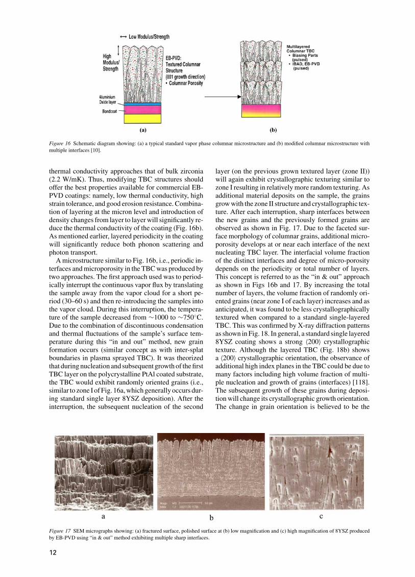
Figure 16 Schematic diagram showing: (a) a typical standard vapor phase columnar microstructure and (b) modified columnar microstructure withmultiple interfaces [10].
thermal conductivity approaches that of bulk zirconia(2.2 W/mK). Thus, modifying TBC structures shouldoffer the best properties available for commercial EB-PVD coatings: namely, low thermal conductivity, highstrain tolerance, and good erosion resistance. Combina-tion of layering at the micron level and introduction ofdensity changes from layer to layer will significantly re-duce the thermal conductivity of the coating (Fig. 16b).As mentioned earlier, layered periodicity in the coatingwill significantly reduce both phonon scattering andphoton transport.
A microstructure similar to Fig. 16b, i.e., periodic in-terfaces and microporosity in the TBC was produced bytwo approaches. The first approach used was to period-ically interrupt the continuous vapor flux by translatingthe sample away from the vapor cloud for a short pe-riod (30–60 s) and then re-introducing the samples intothe vapor cloud. During this interruption, the tempera-ture of the sample decreased from ∼1000 to ∼750◦C.Due to the combination of discontinuous condensationand thermal fluctuations of the sample’s surface tem-perature during this “in and out” method, new grainformation occurs (similar concept as with inter-splatboundaries in plasma sprayed TBC). It was theorizedthat during nucleation and subsequent growth of the firstTBC layer on the polycrystalline PtAl coated substrate,the TBC would exhibit randomly oriented grains (i.e.,similar to zone I of Fig. 16a, which generally occurs dur-ing standard single layer 8YSZ deposition). After theinterruption, the subsequent nucleation of the second
Figure 17 SEM micrographs showing: (a) fractured surface, polished surface at (b) low magnification and (c) high magnification of 8YSZ producedby EB-PVD using “in & out” method exhibiting multiple sharp interfaces.
layer (on the previous grown textured layer (zone II))will again exhibit crystallographic texturing similar tozone I resulting in relatively more random texturing. Asadditional material deposits on the sample, the grainsgrow with the zone II structure and crystallographic tex-ture. After each interruption, sharp interfaces betweenthe new grains and the previously formed grains areobserved as shown in Fig. 17. Due to the faceted sur-face morphology of columnar grains, additional micro-porosity develops at or near each interface of the nextnucleating TBC layer. The interfacial volume fractionof the distinct interfaces and degree of micro-porositydepends on the periodicity or total number of layers.This concept is referred to as the “in & out” approachas shown in Figs 16b and 17. By increasing the totalnumber of layers, the volume fraction of randomly ori-ented grains (near zone I of each layer) increases and asanticipated, it was found to be less crystallographicallytextured when compared to a standard single-layeredTBC. This was confirmed by X-ray diffraction patternsas shown in Fig. 18. In general, a standard single layered8YSZ coating shows a strong 〈200〉 crystallographictexture. Although the layered TBC (Fig. 18b) showsa 〈200〉 crystallographic orientation, the observance ofadditional high index planes in the TBC could be due tomany factors including high volume fraction of multi-ple nucleation and growth of grains (interfaces) [118].The subsequent growth of these grains during deposi-tion will change its crystallographic growth orientation.The change in grain orientation is believed to be the
12
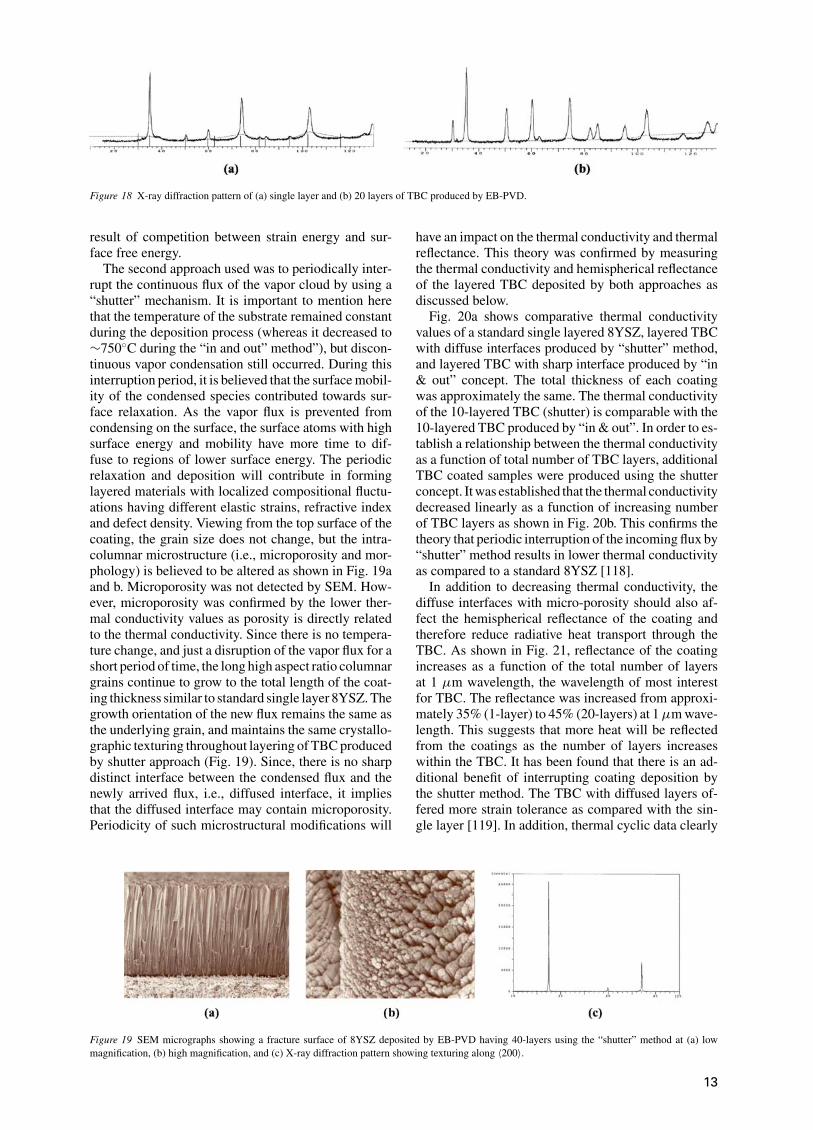
Figure 18 X-ray diffraction pattern of (a) single layer and (b) 20 layers of TBC produced by EB-PVD.
result of competition between strain energy and sur-face free energy.
The second approach used was to periodically inter-rupt the continuous flux of the vapor cloud by using a“shutter” mechanism. It is important to mention herethat the temperature of the substrate remained constantduring the deposition process (whereas it decreased to∼750◦C during the “in and out” method”), but discon-tinuous vapor condensation still occurred. During thisinterruption period, it is believed that the surface mobil-ity of the condensed species contributed towards sur-face relaxation. As the vapor flux is prevented fromcondensing on the surface, the surface atoms with highsurface energy and mobility have more time to dif-fuse to regions of lower surface energy. The periodicrelaxation and deposition will contribute in forminglayered materials with localized compositional fluctu-ations having different elastic strains, refractive indexand defect density. Viewing from the top surface of thecoating, the grain size does not change, but the intra-columnar microstructure (i.e., microporosity and mor-phology) is believed to be altered as shown in Fig. 19aand b. Microporosity was not detected by SEM. How-ever, microporosity was confirmed by the lower ther-mal conductivity values as porosity is directly relatedto the thermal conductivity. Since there is no tempera-ture change, and just a disruption of the vapor flux for ashort period of time, the long high aspect ratio columnargrains continue to grow to the total length of the coat-ing thickness similar to standard single layer 8YSZ. Thegrowth orientation of the new flux remains the same asthe underlying grain, and maintains the same crystallo-graphic texturing throughout layering of TBC producedby shutter approach (Fig. 19). Since, there is no sharpdistinct interface between the condensed flux and thenewly arrived flux, i.e., diffused interface, it impliesthat the diffused interface may contain microporosity.Periodicity of such microstructural modifications will
Figure 19 SEM micrographs showing a fracture surface of 8YSZ deposited by EB-PVD having 40-layers using the “shutter” method at (a) lowmagnification, (b) high magnification, and (c) X-ray diffraction pattern showing texturing along 〈200〉.
have an impact on the thermal conductivity and thermalreflectance. This theory was confirmed by measuringthe thermal conductivity and hemispherical reflectanceof the layered TBC deposited by both approaches asdiscussed below.
Fig. 20a shows comparative thermal conductivityvalues of a standard single layered 8YSZ, layered TBCwith diffuse interfaces produced by “shutter” method,and layered TBC with sharp interface produced by “in& out” concept. The total thickness of each coatingwas approximately the same. The thermal conductivityof the 10-layered TBC (shutter) is comparable with the10-layered TBC produced by “in & out”. In order to es-tablish a relationship between the thermal conductivityas a function of total number of TBC layers, additionalTBC coated samples were produced using the shutterconcept. It was established that the thermal conductivitydecreased linearly as a function of increasing numberof TBC layers as shown in Fig. 20b. This confirms thetheory that periodic interruption of the incoming flux by“shutter” method results in lower thermal conductivityas compared to a standard 8YSZ [118].
In addition to decreasing thermal conductivity, thediffuse interfaces with micro-porosity should also af-fect the hemispherical reflectance of the coating andtherefore reduce radiative heat transport through theTBC. As shown in Fig. 21, reflectance of the coatingincreases as a function of the total number of layersat 1 µm wavelength, the wavelength of most interestfor TBC. The reflectance was increased from approxi-mately 35% (1-layer) to 45% (20-layers) at 1 µm wave-length. This suggests that more heat will be reflectedfrom the coatings as the number of layers increaseswithin the TBC. It has been found that there is an ad-ditional benefit of interrupting coating deposition bythe shutter method. The TBC with diffused layers of-fered more strain tolerance as compared with the sin-gle layer [119]. In addition, thermal cyclic data clearly
13
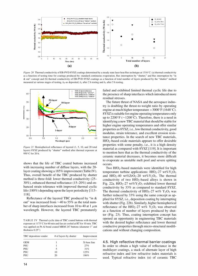
Figure 20 Thermal conductivity of EB-PVD 8YSZ coatings determined by a steady state laser heat flux technique at 1316◦C: (a) thermal conductivityas a function of testing time for coatings produced by: standard continuous evaporation, flux interruption by “shutter,” and flux interruption by “in& out” concept and (b) thermal conductivity of EB-PVD 8YSZ coatings as a function of total number of layers produced by the “shutter” methodmeasured at various stages of testing, k0-as deposited, k2 after 2 h testing and k5 after 5 h testing.
Figure 21 Hemispherical reflectance of layered (1, 5, 10, and 20 totallayers) 8YSZ produced by “shutter” method after thermal exposure at950◦C for 20 h.
shows that the life of TBC coated buttons increasedwith increasing number of diffuse layers, with the 20-layer coating showing a 185% improvement (Table IV).Thus, overall benefit of the TBC produced by shuttermethod is three-fold: lower thermal conductivity (25–30%), enhanced thermal reflectance (15–20%) and en-hanced strain tolerance with improved thermal cycliclife (180%) depending upon the layer periodicity [113–118].
Reflectance of the layered TBC produced by “in &out” was increased from ∼40 to 55% as the total num-ber of sharp interfaces increased from 10 to 40 at 1 µmwavelength. However, the layered TBC prematurely
T ABL E IV Thermal cyclic data of TBC coated buttons with thermalexposure at 1175◦C for 60 min and fan air cooled at RT for 10 min. TBCwas applied on Pt-Al bond coated MRM 247 buttons (diameter 1′′ andthickness 0.25′′)
TBC deposition vendor # of layers by shutter Improvement
OEM 1 X-base linePSU 1 27%PSU 5 31%PSU 10 125%PSU 20 186%
failed and exhibited limited thermal cyclic life due tothe presence of sharp interfaces which introduced moreresidual stresses.
The future thrust of NASA and the aerospace indus-try is doubling the thrust-to-weight ratio by operatingengine at much higher temperature >3000◦F (1648◦C).8YSZ is suitable for engine operating temperatures onlyup to 2200◦F (∼1200◦C). Therefore, there is a need inidentifying a new TBC material that should be stable forhigher engine operating temperatures and offer similarproperties as 8YSZ, i.e., low thermal conductivity, goodmodulus, strain tolerance, and excellent erosion resis-tance properties. In the search of new TBC materials,HfO2-based oxide materials appeare to offer desirableproperties with some penalty, i.e., it is a high densitymaterial as compared with 8YSZ [119]. It is importantto mention here that as the thermal conductivity of theceramic material decreases, it becomes more difficultto evaporate as unstable melt pool and severe spittingoccurs.
Two HfO2-based materials were identified for hightemperature turbine applications: HfO2-27 wt%Y2O3and HfO2-40 wt%ZrO2-20 wt%Y2O3. The thermalconductivity of two HfO2-based alloys is shown inFig. 22a. HfO2-27 wt%Y2O3 exhibited lower thermalconductivity by 33% as compared to standard 8YSZ.The thermal conductivity of HfO2-27 wt% Y2O3 wasfurther reduced by 33% using the same concept as ap-plied for 8YSZ, i.e., deposition coating by interruptingwith shutter (Fig. 22b). Similarly, higher hemisphericalreflectance of the HfO2-27 wt% Y2O3 was observedas a function of number of layers produced by shut-ter (Fig. 23). Thus, coating interruption concept hasopened an opportunity in engineering TBC materialswith the desired higher reflectance and lower thermalconductive properties through micro-structural modifi-cations and without changing composition.
4.5. High reflective thermal barrier coatingsIn order to obtain a high value of reflectance in themultilayer coatings, a stack of alternate layer of highrefractive index and low refractive index materials isused. Typical refractive index (n) of ceramic TBC
14
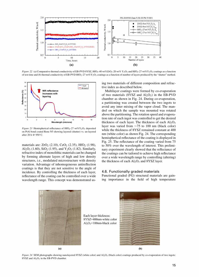
Figure 22 (a) Comparative thermal conductivity of EB-PVD 8YSZ, HfO2-40 wt%ZrO2-20 wt% Y2O3 and HfO2-27 wt%Y2O3 coatings as a functionof test time and (b) thermal conductivity of EB-PVD HfO2-27 wt%Y2O3 coatings as a function of number of layers produced by the “shutter” method.
Figure 23 Hemispherical reflectance of HfO2-27 wt%Y2O3 depositedon PtAl bond coated Rene N5 showing layered (shutter) vs. un-layeredafter 20 h @ 950◦C.
materials are: ZrO2 (2.10), CeO2 (2.35), HfO2 (1.98),Al2O3 (1.60), SiO2 (1.95), and Y2O3 (1.82). Similarly,refractive index of monolithic materials can be changedby forming alternate layers of high and low densitystructures, i.e., modulated microstructure with densityvariation. Advantage of inhomogeneous antireflectioncoatings is that they are not sensitive to the angle ofincidence. By controlling the thickness of each layer,reflectance of the coating can be controlled over a widewavelength range. This concept was demonstrated us-
Figure 24 SEM photographs showing nanolayered 8YSZ (white color) and Al2O3 (black color) coatings produced by co-evaporation of two ingots:8YSZ and Al2O3 in the EB-PVD chamber.
ing two materials of different composition and refrac-tive index as described below.
Multilayer coatings were formed by co-evaporationof two materials (8YSZ and Al2O3) in the EB-PVDchamber as shown in Fig. 24. During co-evaporation,a partitioning was created between the two ingots toavoid any inter mixing of the vapor cloud. The man-drel on which the sample was mounted was rotatedabove the partitioning. The rotation speed and evapora-tion rate of each ingot was controlled to get the desiredthickness of each layer. The thickness of each Al2O3layer was varied from ∼75 to 100 nm (black color)while the thickness of 8YSZ remained constant at 400nm (white color) as shown Fig. 24. The correspondinghemispherical reflectance of the coating is displayed inFig. 25. The reflectance of the coating varied from 75to 50% over the wavelength of interest. This prelimi-nary experiment clearly showed that the reflectance ofthe coatings can be tailored to achieve high reflectanceover a wide wavelength range by controlling (altering)the thickness of each Al2O3 and 8YSZ layer.
4.6. Functionally graded materialsFunctional graded (FG) structural materials are gain-ing importance in the field of high temperature
15
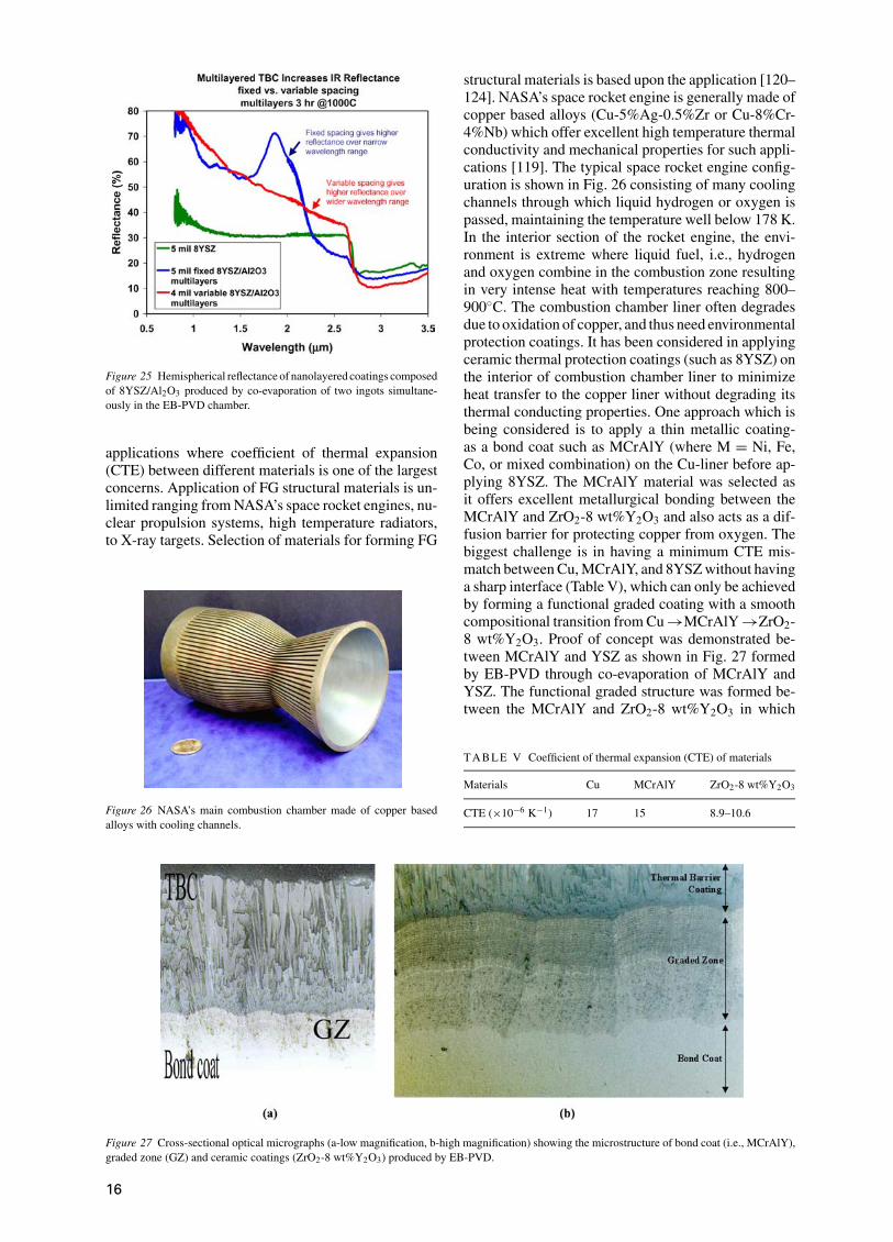
Figure 25 Hemispherical reflectance of nanolayered coatings composedof 8YSZ/Al2O3 produced by co-evaporation of two ingots simultane-ously in the EB-PVD chamber.
applications where coefficient of thermal expansion(CTE) between different materials is one of the largestconcerns. Application of FG structural materials is un-limited ranging from NASA’s space rocket engines, nu-clear propulsion systems, high temperature radiators,to X-ray targets. Selection of materials for forming FG
Figure 26 NASA’s main combustion chamber made of copper basedalloys with cooling channels.
Figure 27 Cross-sectional optical micrographs (a-low magnification, b-high magnification) showing the microstructure of bond coat (i.e., MCrAlY),graded zone (GZ) and ceramic coatings (ZrO2-8 wt%Y2O3) produced by EB-PVD.
structural materials is based upon the application [120–124]. NASA’s space rocket engine is generally made ofcopper based alloys (Cu-5%Ag-0.5%Zr or Cu-8%Cr-4%Nb) which offer excellent high temperature thermalconductivity and mechanical properties for such appli-cations [119]. The typical space rocket engine config-uration is shown in Fig. 26 consisting of many coolingchannels through which liquid hydrogen or oxygen ispassed, maintaining the temperature well below 178 K.In the interior section of the rocket engine, the envi-ronment is extreme where liquid fuel, i.e., hydrogenand oxygen combine in the combustion zone resultingin very intense heat with temperatures reaching 800–900◦C. The combustion chamber liner often degradesdue to oxidation of copper, and thus need environmentalprotection coatings. It has been considered in applyingceramic thermal protection coatings (such as 8YSZ) onthe interior of combustion chamber liner to minimizeheat transfer to the copper liner without degrading itsthermal conducting properties. One approach which isbeing considered is to apply a thin metallic coating-as a bond coat such as MCrAlY (where M = Ni, Fe,Co, or mixed combination) on the Cu-liner before ap-plying 8YSZ. The MCrAlY material was selected asit offers excellent metallurgical bonding between theMCrAlY and ZrO2-8 wt%Y2O3 and also acts as a dif-fusion barrier for protecting copper from oxygen. Thebiggest challenge is in having a minimum CTE mis-match between Cu, MCrAlY, and 8YSZ without havinga sharp interface (Table V), which can only be achievedby forming a functional graded coating with a smoothcompositional transition from Cu →MCrAlY →ZrO2-8 wt%Y2O3. Proof of concept was demonstrated be-tween MCrAlY and YSZ as shown in Fig. 27 formedby EB-PVD through co-evaporation of MCrAlY andYSZ. The functional graded structure was formed be-tween the MCrAlY and ZrO2-8 wt%Y2O3 in which
TABLE V Coefficient of thermal expansion (CTE) of materials
Materials Cu MCrAlY ZrO2-8 wt%Y2O3
CTE (×10−6 K−1) 17 15 8.9–10.6
16
during the co-evaporation period, the evaporation rateof MCrAlY was decreased and evaporation rate ofZrO2-8 wt%Y2O3 was increased resulting in FG zone(Fig. 27). The deposition was continued with only YSZbeing evaporated to form a top layer composed onlyof the ceramic coating, i.e., ZrO2-8 wt%Y2O3. Futureefforts would entail applying a layer of copper coatingfollowed by co-evaporation of copper and MCrAlY onthe combustion chamber liner to achieve good metal-lurgical bonding with the base material.
4.6.1. Functional graded Re → ReHf → Hf→ HfN and Re → ReZr → Zr → ZrNcoatings
A similar research effort was undertaken in applyingHfN and ZrN coatings as a diffusion barrier on Re-Mo based alloy substrate for high temperature appli-cations. One such application is for light-weight heatpipe cooled leading edges with high heat flux capa-bilities, where refractory-metal tubes embedded in therefractory-composite structure serve as the containersfor liquid-metal heat pipe for space application [125].Refractory metals are utilized since they exhibit highmelting points and high strengths at elevated tempera-tures. They can also withstand high processing temper-atures required for manufacturing refractory-compositematerials. One of the complications encountered withembedding a refractory-metal tube in a refractory-composite structure is lack of chemical compatibil-ity between the two materials. Many refractory metalsform carbides or silicides when in contact with carbonor silicon at elevated temperatures. The formation ofcarbide and silicides can lower the strength and ductil-ity of the refractory metals. In addition, for heat pipeapplications, carbon or silicon may diffuse through themetal tube (i.e., heat-pipe container) and contaminatethe heat pipe. In order to minimize chemical interac-tion between the refractory-metal heat pipe tube andrefractory-composite structure, various barrier coatingsare being considered. One of the diffusion barrier coat-
Figure 28 (a) SEM showing the top view of the coating exhibiting nano-grained microstructure, (b) cross-section scanning electron micrograph(SEM) shows a functionally graded Re → ReHf → Hf material deposited on Re-Mo alloy plate by EB-PVD [126].
ings identified is HfN and ZrN. The biggest challengewas to minimize delamination of the coating duringthermal cyclic exposure caused by large CTE mismatchand poor interfaces. Functionally graded Re → ReHf→ Hf → HfN structure was made by ion beam assistedEB-PVD as shown in Fig. 28. Here, Re was evapo-rated first followed by the co-evaporation of Re and Hf.Concentration of Hf was continuously increased andRe was decreased as a function of deposition time andcoating build-up, resulting in the last layer enrichedin Hf (100%). This Hf layer was then reacted withionized nitrogen gas during deposition process form-ing HfN. There is no distinct interface between the Hfand the HfN structure. Fig. 28a shows the top view ofthe HfN coating exhibiting nano-grained microstruc-ture. Fig. 28b shows the cross section of the functionalgraded coatings (Re → ReHf → Hf → HfN). It isunclear the cause of variation in the cross section mi-crostructure of the functional graded coating in spite ofcontinuous evaporation of Re → Hf materials withoutinterruption.
4.7. Precision net-shapedforming components
Refractory metals are very attractive materials for hightemperature structural and energy system applicationssuch as solar powered rocket engines, heat exchang-ers, space and missile propulsion systems. However, itis very difficult to produce precision net-shaped com-ponents made of refractory metals such as tungsten,hafnium and rhenium with a density >95%. Typically,components are fabricated by either powder metallurgy(P/M) or chemical vapor deposition (CVD). Due to dif-ficulties encountered in the P/M fabrication and shapingof refractory parts, CVD is mainly used in fabricatingthin walled, small diameter or complex shaped com-ponents and also for coatings on carbon, ceramic andmetal components. However, the CVD process also hasmany shortcomings. For instance, rhenium depositionis obtained by passing chlorine gas through a heated
17
chamber (at 500◦C) containing rhenium chips result-ing in rhenium penta-chloride (ReCl5). The gaseousmolecules of ReCl5 decompose at 1200◦C with rhe-nium atoms depositing on the substrate. However, CVDrhenium deposits contain entrapped gases (chlorine andhydrogen) as impurities resulting in lower physical andmechanical properties. CVD coating often producescolumnar microstructure that is undesirable for struc-tural applications. The columnar microstructure is de-stroyed by periodically removing partially coated com-ponents followed by mechanical grinding, i.e., partiallyremoving rhenium coating material and continue re-coating. This effort is repeated many times to obtainthe desired thickness and density of the coating. It hasbeen reported that the CVD rhenium substrate producedin this way exhibits multiple layers. When the CVD-Recomponent is heated to elevated temperature, individ-ual layers tend to separate, allowing slippage. This phe-nomenon has shown to decrease the mechanical prop-erties of CVD-Re, which is highly undesirable for thedesign and incorporation of flight engines [127, 128].The second shortcoming of the CVD process is thatit requires long fabrication time in producing compo-nents, and thus it is not a cost effective manufacturingprocess.
Since CVD is not a line-of-sight process, the in-terior and exterior of complex components can becoated simultaneously. However, it is difficult to ap-ply uniform coating ‘thickness’ on spherical compo-nents, i.e., graphite balls due to limited flexibility inmaneuvering parts in the reaction chamber, gas flowdynamics and entire surface area to be coated simul-taneously (i.e., 360◦). Depending on the dimensionof the components, generally one component (such asthruster) is manufactured at a time in the CVD reactorchamber.
Powder metallurgy (P/M) techniques have been ex-plored in the fabrication of rhenium components [129].These techniques also have their limitations with re-spect to cost, speed, achievable geometry, required tool-ing and high temperature isostatic pressure (HIP) treat-ment for compaction [130]. Various steps are involvedin the manufacturing of components including cold iso-static pressing, pre-sintering at 1200◦C and hot sinter-ing at 2500◦C. Densities greater than 99% are achiev-able only after extensive amounts of accumulated coldand hot working. Hot working of rhenium must be car-ried out in a hydrogen environment. In air, the rhe-nium metal readily oxidizes to the heptoxide (meltingpoint 297◦C), so hot working in air is not possible. Thisextensive value-added processing contributes to highcost and fairly limited range of commercial shape com-ponents [131]. Fabrication of components by powder-plasma spray process has also been explored and ex-hibits poor mechanical properties due to presence oflarge volume fraction of porosity.
An effort was undertaken to address shortcomings ofCVD and P/M techniques and identify an alternativemanufacturing method in fabricating net shaped com-ponents with density >95% in a cost effective manner.Electron beam-physical vapor deposition (EB-PVD)method has met these challenges.
4.7.1. Fabrication of rhenium plateEffort was first undertaken to demonstrate that rheniumplates produced by EB-PVD had equivalent or betterphysical and mechanical properties in comparison withconventional CVD process. Rhenium ingot was usedas a source material that was supplied by Rhenium Al-loys Inc. (density 98% and purity 99.99%). A focusedhigh-energy electron beam was used to evaporate therhenium ingot in the coating chamber and deposited ongraphite plates. During deposition process, the graphiteplates were indirectly heated up to 1000◦C. The mi-crostructure of the coating was tailored by changingvarious process parameters including evaporation rate,periodically interrupting incoming vapor flux, and va-por incidence angle (VIA) as shown in Fig. 29, respec-tively [131, 132]. A novel concept was developed toavoid any continuous columnar grain formation dur-ing deposition, i.e., used the in & out approach informing textured subgrain microstructure as shown inFig. 29b. In addition, rhenium plate exhibited texturedgrain growth with micron and sub-micron sized mi-crostructure. Coated plates exhibited higher hardness(283VHN) in comparison with CVD rhenium plate withhardness of 245VHN. Using the Hall-Petch equationalong with the grain size and hardness, it is predictedthat the Re-plate will exhibit 30% improvement in me-chanical properties as compared with CVD Re-plate,which was confirmed by measuring mechanical prop-erties (tensile strength of EB-PVD Re was ∼72 ksi andCVD Re was ∼50 ksi). Rhenium plates were found tobe free from impurities such as copper or other ma-terials. During the course of this investigation, it wasdemonstrated that the growth orientation of the coatingscan be changed by periodically changing the vapor in-cidence angle (VIA) of the incoming flux as shown inFig. 29c.
4.7.2. Fabrication of rhenium coatedgraphite balls
Applying uniform rhenium coating on graphite balls(or cores) by EB-PVD is a demonstration in net-shape forming components. 17 graphite cores (diameter∼15 mm) were simultaneously charged into a cylindri-cal cage as shown in Fig. 30a. The cage was fabricatedusing molybdenum wire mesh. The cylindrical cagewas rotated at 7–10 rpm above the melt pool within therhenium vapor. During the deposition process, coreswere heated to 1000◦C by radiation heating under theA-frame graphite heater. The Re-coated graphite coreswere also simultaneously bombarded with ionized ar-gon gas during deposition to obtain a dense uniformmicrostructure. After applying rhenium to the full coat-ing thickness, seventeen coated cores were simulta-neously polished in the laboratory vibromet-polishingunit to the surface finish <Ra8 (Fig. 30b). All coatedcores exhibited uniform coatings with 100% concen-tricity, which was measured by co-ordinate measuringmachine (CMC). It is important to mention here thatthere are more than 250 micron and sub-micron grainsthrough the coating thickness (2000 µm) with a muchfiner grain structure (Fig. 31).
18
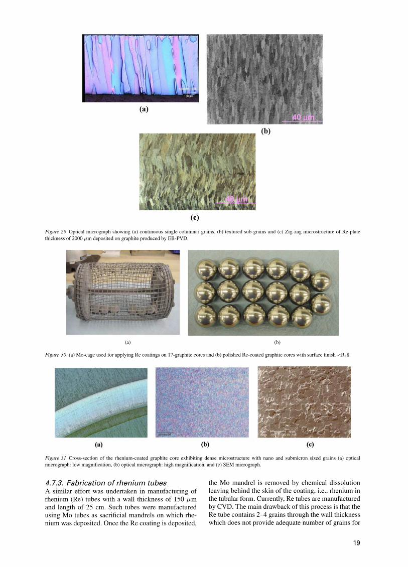
Figure 29 Optical micrograph showing (a) continuous single columnar grains, (b) textured sub-grains and (c) Zig-zag microstructure of Re-platethickness of 2000 µm deposited on graphite produced by EB-PVD.
(a) (b)
Figure 30 (a) Mo-cage used for applying Re coatings on 17-graphite cores and (b) polished Re-coated graphite cores with surface finish <Ra8.
Figure 31 Cross-section of the rhenium-coated graphite core exhibiting dense microstructure with nano and submicron sized grains (a) opticalmicrograph: low magnification, (b) optical micrograph: high magnification, and (c) SEM micrograph.
4.7.3. Fabrication of rhenium tubesA similar effort was undertaken in manufacturing ofrhenium (Re) tubes with a wall thickness of 150 µmand length of 25 cm. Such tubes were manufacturedusing Mo tubes as sacrificial mandrels on which rhe-nium was deposited. Once the Re coating is deposited,
the Mo mandrel is removed by chemical dissolutionleaving behind the skin of the coating, i.e., rhenium inthe tubular form. Currently, Re tubes are manufacturedby CVD. The main drawback of this process is that theRe tube contains 2–4 grains through the wall thicknesswhich does not provide adequate number of grains for
19
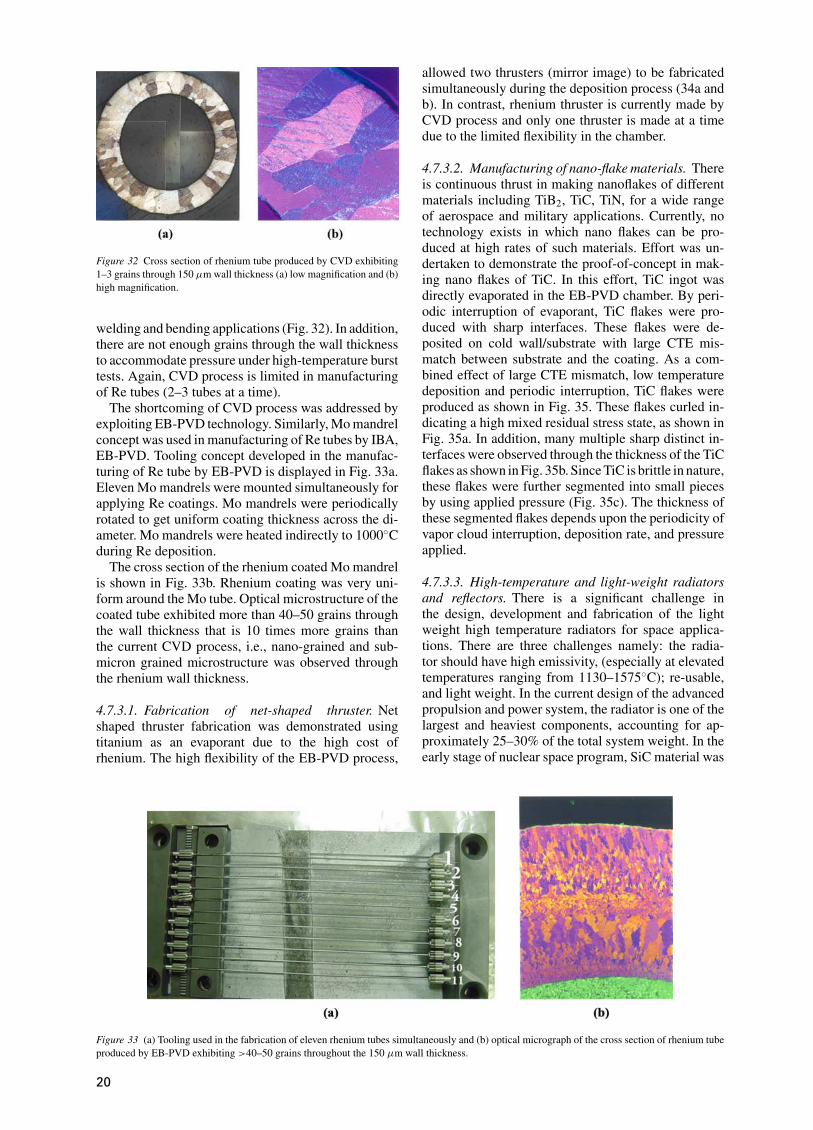
Figure 32 Cross section of rhenium tube produced by CVD exhibiting1–3 grains through 150 µm wall thickness (a) low magnification and (b)high magnification.
welding and bending applications (Fig. 32). In addition,there are not enough grains through the wall thicknessto accommodate pressure under high-temperature bursttests. Again, CVD process is limited in manufacturingof Re tubes (2–3 tubes at a time).
The shortcoming of CVD process was addressed byexploiting EB-PVD technology. Similarly, Mo mandrelconcept was used in manufacturing of Re tubes by IBA,EB-PVD. Tooling concept developed in the manufac-turing of Re tube by EB-PVD is displayed in Fig. 33a.Eleven Mo mandrels were mounted simultaneously forapplying Re coatings. Mo mandrels were periodicallyrotated to get uniform coating thickness across the di-ameter. Mo mandrels were heated indirectly to 1000◦Cduring Re deposition.
The cross section of the rhenium coated Mo mandrelis shown in Fig. 33b. Rhenium coating was very uni-form around the Mo tube. Optical microstructure of thecoated tube exhibited more than 40–50 grains throughthe wall thickness that is 10 times more grains thanthe current CVD process, i.e., nano-grained and sub-micron grained microstructure was observed throughthe rhenium wall thickness.
4.7.3.1. Fabrication of net-shaped thruster. Netshaped thruster fabrication was demonstrated usingtitanium as an evaporant due to the high cost ofrhenium. The high flexibility of the EB-PVD process,
Figure 33 (a) Tooling used in the fabrication of eleven rhenium tubes simultaneously and (b) optical micrograph of the cross section of rhenium tubeproduced by EB-PVD exhibiting >40–50 grains throughout the 150 µm wall thickness.
allowed two thrusters (mirror image) to be fabricatedsimultaneously during the deposition process (34a andb). In contrast, rhenium thruster is currently made byCVD process and only one thruster is made at a timedue to the limited flexibility in the chamber.
4.7.3.2. Manufacturing of nano-flake materials. Thereis continuous thrust in making nanoflakes of differentmaterials including TiB2, TiC, TiN, for a wide rangeof aerospace and military applications. Currently, notechnology exists in which nano flakes can be pro-duced at high rates of such materials. Effort was un-dertaken to demonstrate the proof-of-concept in mak-ing nano flakes of TiC. In this effort, TiC ingot wasdirectly evaporated in the EB-PVD chamber. By peri-odic interruption of evaporant, TiC flakes were pro-duced with sharp interfaces. These flakes were de-posited on cold wall/substrate with large CTE mis-match between substrate and the coating. As a com-bined effect of large CTE mismatch, low temperaturedeposition and periodic interruption, TiC flakes wereproduced as shown in Fig. 35. These flakes curled in-dicating a high mixed residual stress state, as shown inFig. 35a. In addition, many multiple sharp distinct in-terfaces were observed through the thickness of the TiCflakes as shown in Fig. 35b. Since TiC is brittle in nature,these flakes were further segmented into small piecesby using applied pressure (Fig. 35c). The thickness ofthese segmented flakes depends upon the periodicity ofvapor cloud interruption, deposition rate, and pressureapplied.
4.7.3.3. High-temperature and light-weight radiatorsand reflectors. There is a significant challenge inthe design, development and fabrication of the lightweight high temperature radiators for space applica-tions. There are three challenges namely: the radia-tor should have high emissivity, (especially at elevatedtemperatures ranging from 1130–1575◦C); re-usable,and light weight. In the current design of the advancedpropulsion and power system, the radiator is one of thelargest and heaviest components, accounting for ap-proximately 25–30% of the total system weight. In theearly stage of nuclear space program, SiC material was
20
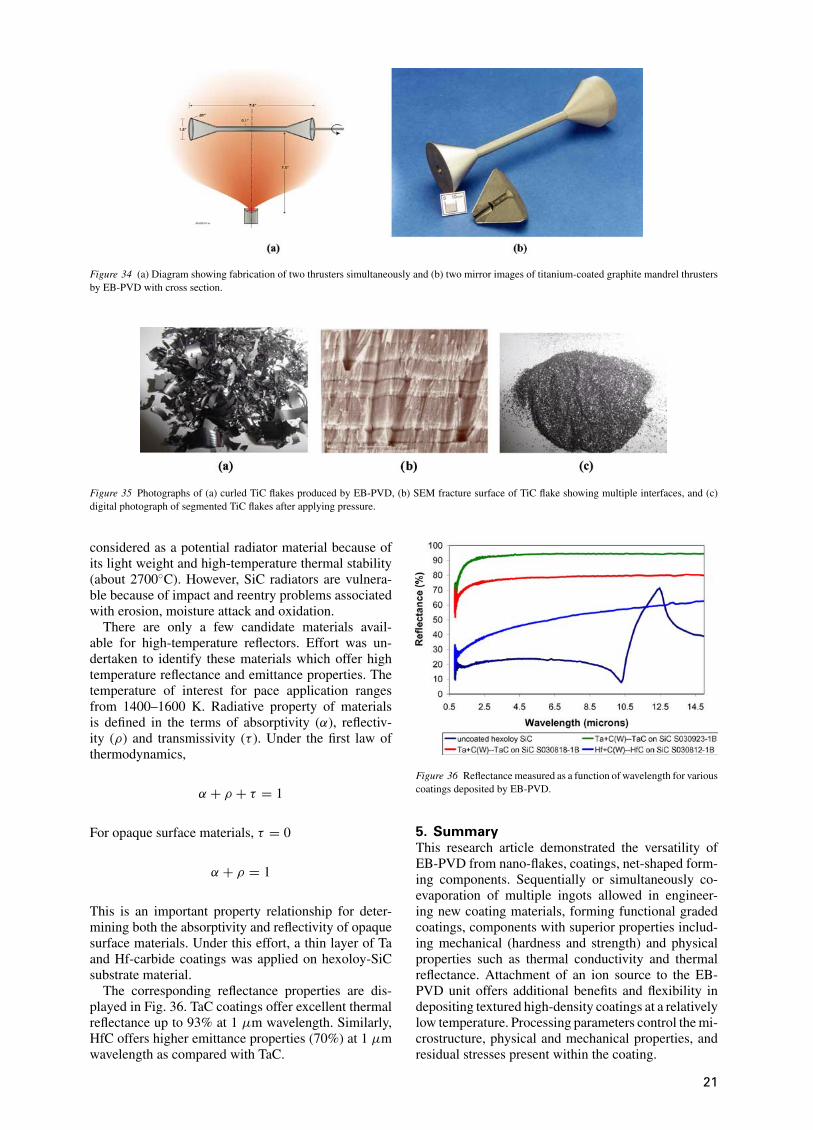
Figure 34 (a) Diagram showing fabrication of two thrusters simultaneously and (b) two mirror images of titanium-coated graphite mandrel thrustersby EB-PVD with cross section.
Figure 35 Photographs of (a) curled TiC flakes produced by EB-PVD, (b) SEM fracture surface of TiC flake showing multiple interfaces, and (c)digital photograph of segmented TiC flakes after applying pressure.
considered as a potential radiator material because ofits light weight and high-temperature thermal stability(about 2700◦C). However, SiC radiators are vulnera-ble because of impact and reentry problems associatedwith erosion, moisture attack and oxidation.
There are only a few candidate materials avail-able for high-temperature reflectors. Effort was un-dertaken to identify these materials which offer hightemperature reflectance and emittance properties. Thetemperature of interest for pace application rangesfrom 1400–1600 K. Radiative property of materialsis defined in the terms of absorptivity (α), reflectiv-ity (ρ) and transmissivity (τ ). Under the first law ofthermodynamics,
α + ρ + τ = 1
For opaque surface materials, τ = 0
α + ρ = 1
This is an important property relationship for deter-mining both the absorptivity and reflectivity of opaquesurface materials. Under this effort, a thin layer of Taand Hf-carbide coatings was applied on hexoloy-SiCsubstrate material.
The corresponding reflectance properties are dis-played in Fig. 36. TaC coatings offer excellent thermalreflectance up to 93% at 1 µm wavelength. Similarly,HfC offers higher emittance properties (70%) at 1 µmwavelength as compared with TaC.
Figure 36 Reflectance measured as a function of wavelength for variouscoatings deposited by EB-PVD.
5. SummaryThis research article demonstrated the versatility ofEB-PVD from nano-flakes, coatings, net-shaped form-ing components. Sequentially or simultaneously co-evaporation of multiple ingots allowed in engineer-ing new coating materials, forming functional gradedcoatings, components with superior properties includ-ing mechanical (hardness and strength) and physicalproperties such as thermal conductivity and thermalreflectance. Attachment of an ion source to the EB-PVD unit offers additional benefits and flexibility indepositing textured high-density coatings at a relativelylow temperature. Processing parameters control the mi-crostructure, physical and mechanical properties, andresidual stresses present within the coating.
21
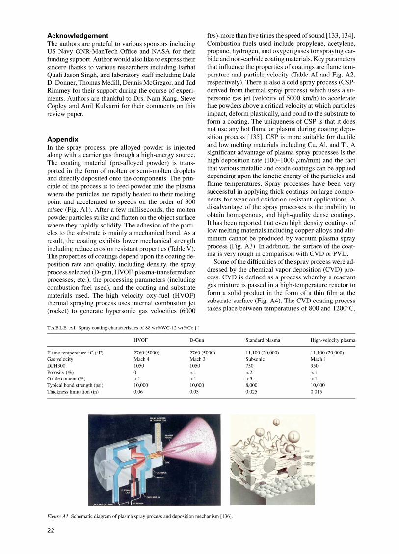
AcknowledgementThe authors are grateful to various sponsors includingUS Navy ONR-ManTech Office and NASA for theirfunding support. Author would also like to express theirsincere thanks to various researchers including FarhatQuali Jason Singh, and laboratory staff including DaleD. Donner, Thomas Medill, Dennis McGregor, and TadRimmey for their support during the course of experi-ments. Authors are thankful to Drs. Nam Kang, SteveCopley and Anil Kulkarni for their comments on thisreview paper.
AppendixIn the spray process, pre-alloyed powder is injectedalong with a carrier gas through a high-energy source.The coating material (pre-alloyed powder) is trans-ported in the form of molten or semi-molten dropletsand directly deposited onto the components. The prin-ciple of the process is to feed powder into the plasmawhere the particles are rapidly heated to their meltingpoint and accelerated to speeds on the order of 300m/sec (Fig. A1). After a few milliseconds, the moltenpowder particles strike and flatten on the object surfacewhere they rapidly solidify. The adhesion of the parti-cles to the substrate is mainly a mechanical bond. As aresult, the coating exhibits lower mechanical strengthincluding reduce erosion resistant properties (Table V).The properties of coatings depend upon the coating de-position rate and quality, including density, the sprayprocess selected (D-gun, HVOF, plasma-transferred arcprocesses, etc.), the processing parameters (includingcombustion fuel used), and the coating and substratematerials used. The high velocity oxy-fuel (HVOF)thermal spraying process uses internal combustion jet(rocket) to generate hypersonic gas velocities (6000
T ABL E AI Spray coating characteristics of 88 wt%WC-12 wt%Co [ ]
HVOF D-Gun Standard plasma High-velocity plasma
Flame temperature ◦C (◦F) 2760 (5000) 2760 (5000) 11,100 (20,000) 11,100 (20,000)Gas velocity Mach 4 Mach 3 Subsonic Mach 1DPH300 1050 1050 750 950Porosity (%) 0 <1 <2 <1Oxide content (%) <1 <1 <3 <1Typical bond strength (psi) 10,000 10,000 8,000 10,000Thickness limitation (in) 0.06 0.03 0.025 0.015
Figure A1 Schematic diagram of plasma spray process and deposition mechanism [136].
ft/s)-more than five times the speed of sound [133, 134].Combustion fuels used include propylene, acetylene,propane, hydrogen, and oxygen gases for spraying car-bide and non-carbide coating materials. Key parametersthat influence the properties of coatings are flame tem-perature and particle velocity (Table AI and Fig. A2,respectively). There is also a cold spray process (CSP-derived from thermal spray process) which uses a su-personic gas jet (velocity of 5000 km/h) to acceleratefine powders above a critical velocity at which particlesimpact, deform plastically, and bond to the substrate toform a coating. The uniqueness of CSP is that it doesnot use any hot flame or plasma during coating depo-sition process [135]. CSP is more suitable for ductileand low melting materials including Cu, Al, and Ti. Asignificant advantage of plasma spray processes is thehigh deposition rate (100–1000 µm/min) and the factthat various metallic and oxide coatings can be applieddepending upon the kinetic energy of the particles andflame temperatures. Spray processes have been verysuccessful in applying thick coatings on large compo-nents for wear and oxidation resistant applications. Adisadvantage of the spray processes is the inability toobtain homogenous, and high-quality dense coatings.It has been reported that even high density coatings oflow melting materials including copper-alloys and alu-minum cannot be produced by vacuum plasma sprayprocess (Fig. A3). In addition, the surface of the coat-ing is very rough in comparison with CVD or PVD.
Some of the difficulties of the spray process were ad-dressed by the chemical vapor deposition (CVD) pro-cess. CVD is defined as a process whereby a reactantgas mixture is passed in a high-temperature reactor toform a solid product in the form of a thin film at thesubstrate surface (Fig. A4). The CVD coating processtakes place between temperatures of 800 and 1200◦C,
22
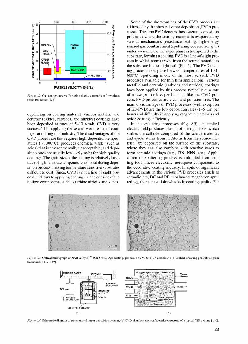
Figure A2 Gas temperature vs. Particle velocity comparison for variousspray processes [136].
depending on coating material. Various metallic andceramic (oxides, carbides, and nitrides) coatings havebeen deposited at rates of 5–10 µm/h. CVD is verysuccessful in applying dense and wear resistant coat-ings for cutting tool industry. The disadvantages of theCVD process are that requires high-deposition temper-atures (>1000◦C); produces chemical waste (such asacids) that is environmentally unacceptable; and depo-sition rates are usually low (<5 µm/h) for high-qualitycoatings. The grain size of the coating is relatively largedue to high substrate temperature exposed during depo-sition process, making temperature sensitive substratesdifficult to coat. Since, CVD is not a line of sight pro-cess, it allows to applying coatings in and out side of thehollow components such as turbine airfoils and vanes.
Figure A3 Optical micrograph of NAR-alloy ZTM (Cu-5 wt% Ag) coatings produced by VPS (a) un-etched and (b) etched: showing porosity at grainboundaries [137–139].
(a) (b)
Figure A4 Schematic diagram of (a) chemical vapor deposition system, (b) CVD chamber, and surface microstructure of a typical TiN coating [140].
Some of the shortcomings of the CVD process areaddressed by the physical vapor deposition (PVD) pro-cesses. The term PVD denotes those vacuum depositionprocesses where the coating material is evaporated byvarious mechanisms (resistance heating, high-energyionized gas bombardment (sputtering), or electron gun)under vacuum, and the vapor phase is transported to thesubstrate, forming a coating. PVD is a line-of-sight pro-cess in which atoms travel from the source material tothe substrate in a straight path (Fig. 3). The PVD coat-ing process takes place between temperatures of 100–600◦C. Sputtering is one of the most versatile PVDprocesses available for thin film applications. Variousmetallic and ceramic (carbides and nitrides) coatingshave been applied by this process typically at a rateof a few µm or less per hour. Unlike the CVD pro-cess, PVD processes are clean and pollution free. Themain disadvantages of PVD processes (with exceptionof EB-PVD) are the low deposition rates (1–5 µm perhour) and difficulty in applying magnetic materials andoxide coatings efficiently.
In the sputtering processes (Fig. A5), an appliedelectric field produces plasma of inert-gas ions, whichstrikes the cathode composed of the source material,and ejects atoms from it. Atoms from the source ma-terial are deposited on the surface of the substrate,where they can also combine with reactive gases toform ceramic coatings (e.g., TiN, NbN, etc.). Appli-cation of sputtering process is unlimited from cut-ting tool, micro-electronic, aerospace components tothe decorative coating industry. In spite of significantadvancements in the various PVD processes (such ascathodic-arc, DC and RF unbalanced-magnetron sput-tering), there are still drawbacks in coating quality. For
23
Figure A5 Schematic diagram of sputtering mechanism and SEM photograph of TiN deposited by sputtering [141].
example, the cathodic-arc PVD process produces liq-uid droplets or macro-particles of metals, 1 to 15 µmin size, during the evaporation of the target material.These molten particles can be entrapped in the growingfilm, resulting in inhomogeneity in the microstructureand detrimental physical properties.
Ion implantation is not a deposition process, butrather a surface modification process in which appro-priate atoms are embedded in a material through high-energy beams. High-energy ions are produced in anaccelerator and directed on the surface of the substrate.A high-energy ion implanter (1–10 MeV) is requiredfor deep penetration (∼5 µm). Ionized particles enterinto the substrate with kinetic energies four to five or-ders of magnitude greater than the binding energy ofthe solid by a collision mechanism. The principal ap-plication of ion implantation has been in the electronicindustries. Typical application of ion implantation is inthe bearing, gear, and biomedical industries. The maindisadvantage of the ion implantation process is the lim-ited depth of penetration into the substrate (<5 µm)and the long processing times.
Ion plating is a derivative of ion implantation inwhich the substrate is made the cathode and the sourcematerial is thermally evaporated before being partiallyionized and accelerated to the substrate (cathode). Byproper selection of materials and gas, carbides, nitrides,and oxides can be deposited. Potential applications ofion plating are in tooling industries and certain aircraftcomponents. The disadvantages of the above mentionedPVD processes can be addressed by the ion beam as-sisted, EB-PVD process.
References1. J . S O B O T A, G. S O R E N S E N, H. J E N S E N, Z .
B O C H N I C E K and V. H O L Y , Surf. Coat. Techn. 142–144 (2001)590.
2. K . C . C H I N, A. G O H E L, H. I . E L I M, W. J I , G . L .C H O N G, K. Y. L I M, C . H. S O W and A. T . S . W E E ,Chem. Phys. Lett. 383(1/2) (2004) 72.
3. M. B R O G R E N, G. L . H A R D I N G, R . K A R M H A G, C.G. R I B B I N G, G. A. N I K L A S S O N and L . S T E N M A R K ,Thin Solid Films 370(1/2) (2000) 268.
4. Q . X I A N G, Y. Z H O U, B. S . O O I , Y . L . L A M, Y. C .C H A N and C. H. K A M , ibid. 370(1/2) (2000) 243.
5. H . H O L L E C K , “Design of Nanostructured Thin Films for Tri-bological Applications,” TMS Conference Proceedings on SurfaceEngineering: Science and Technology I, edited by A. Kumar, Y.W. Chung, J. J. Moore and J. E. Smugeresky (1999) p. 207.
6. J . R . N I C H O L L S , K. J . L A W S O N, D. S . R I C K E R B Y
and P . M O R R E L L “Advanced Processing of TBC for ReducedThermal Conductivity,” AGARD SMP Meeting on “Thermal Bar-rier Coatings” Aalborg, Denmark, 15–16, Oct. 1997, p. 6-1 to 6–7.
7. R . A . M I L L E R , “Thermal Barrier Coatings for Aircraft Engines-History and Directions,” Thermal Barrier Coating Workshop,NASA CP 3312, 1995, p. 17.
8. O . U N A L, T . E . M I T C H E L L and A. H. H E U E R , J. Amer.Ceram. Soc. 77(4) (1994) 984.
9. R . A . M I L L E R , Surf. Coat. Techn. 30 (1987) 1.10. J . S I N G H, D. E . W O L F E and J A S O N S I N G H , J. Mater.
Sci. 37 (2002) 3261.11. K . L . C H O Y , Prog. Mater. Sci. 48(2) (2003) 57.12. S .V . B A T T Y, T . R I C H A R D S O N, P . P E T C O C K and L .
R A M A N , Thin Solid Films 266(2) (1995) 96.13. D . E . W O L F E , Thesis 1996MSWolfe DE, Penn State University,
2001.14. R . B U N S H A H (ed.) “Handbook of Deposition Technologies for
Films and Coatings” (Noyes Publications, Park Ridge, N.J., 1994).15. M. H O C K I N G , “Metallic and Ceramic Coatings, Longman Sci-
entific and Technical” (John Wiley and Sons Inc., 1989).16. R. J. Hill (ed.), “Physical Vapor Deposition,” Temescal, a Division
of the BOC Group, Inc., Berkeley, CA (1986).17. R . M C I N T Y R E , Mater. Proc. 8 (1996) 455.18. J . S I N G H , J. Mater. Sci. 29 (1994) 5232.19. Y O N G-J U N T A N and K I M Y O N G L I M , Surf. Coat. Techn.,
167(2/3) (2003) 255.20. S . S A F A I E , L . F . P O C H E T and P . H O W A R D , ibid.
94/95(1/3) (1997) 70.21. S V E N D S. E S K I L D S E N , ibid. 116–119 (1999) 18.22. W. B E E L E, G. M A R I J N I S S E N and A. V A N L I E S H O U T ,
ibid. 120/121 (1999) 61.23. P . F A U C H A I S and A. V A R D E L L E , Intern. J. Therm. Sci.
39(9–11) (2000) 852.24. J . R . P I E R C E , “Theory of Design of Electronic Beams,” D. Van
Nostrand Company Inc., New York, New York (1954).25. D . E . W O L F E and J . S I N G H , J. Mater. Sci. 33 (1998) 3677.26. H . H O L L E C K “Design of Nanostructured Thin Films for Tri-
bological Applications,” TMS Conference Proceedings on SurfaceEngineering: Science and Technology I, edited by A. Kumar, Y.W. Chung, J. J. Moore and J. E. Smugeresky (1999) p. 207.
27. D . E . W O L F E, M. M O V C H A N and J . S I N G H , “Architec-ture of Functionally Gradient Ceramic-Metallic Coatings By EB-PVD for High Temperature Applications,” Proceedings of Pro-ceeding of Advances in Coating Technologies, at TMS AnnualMeeting at Orlando, edited by C. R. Clayton and J. K. Hirvonen(TMS, 1997) p. 93.
28. D . E . W O L F E J . S I N G H and K. N A R A S I M H A N , J. Surf.Coat. Techn. 165 (2003) 8.
29. D O U G L A S E. W O L F E , “Synthesis and characterization of TiC,TiBCN, TiB2/TiC, and TiC/CrC multilayer coatings by reactive andion beam-assisted, electron beam-physical vapor deposition (EB-PVD)” Thesis 2001D Wolfe DE, Penn State University, UniversityPark, PA, 2001.
30. O . A U C I E L L O, M. S . A M E E N, A. R . K R A U S S , A.I . K I N G O N and D. J . L I C H T E N W A L N E R , “Surface Mod-ification Technologies IV,” edited by T. S. Sudarshan, D. G. Bhat
24
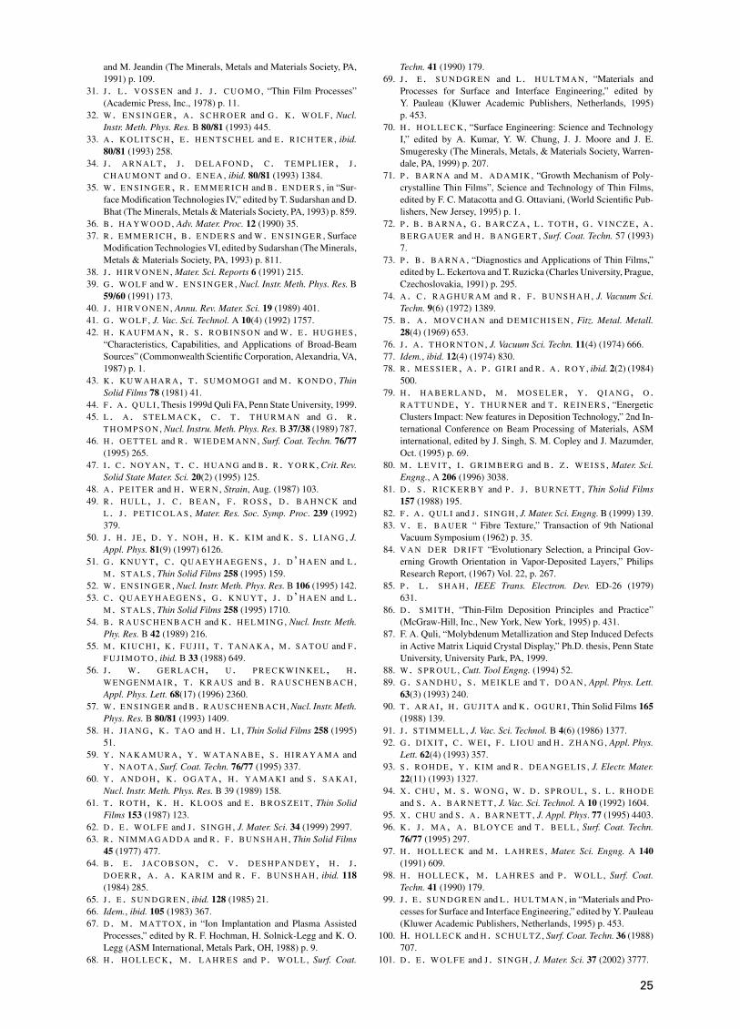
and M. Jeandin (The Minerals, Metals and Materials Society, PA,1991) p. 109.
31. J . L . V O S S E N and J . J . C U O M O , “Thin Film Processes”(Academic Press, Inc., 1978) p. 11.
32. W. E N S I N G E R, A. S C H R O E R and G. K. W O L F , Nucl.Instr. Meth. Phys. Res. B 80/81 (1993) 445.
33. A . K O L I T S C H, E . H E N T S C H E L and E . R I C H T E R , ibid.80/81 (1993) 258.
34. J . A R N A L T, J . D E L A F O N D, C. T E M P L I E R, J .C H A U M O N T and O. E N E A , ibid. 80/81 (1993) 1384.
35. W. E N S I N G E R, R . E M M E R I C H and B. E N D E R S , in “Sur-face Modification Technologies IV,” edited by T. Sudarshan and D.Bhat (The Minerals, Metals & Materials Society, PA, 1993) p. 859.
36. B . H A Y W O O D , Adv. Mater. Proc. 12 (1990) 35.37. R . E M M E R I C H, B . E N D E R S and W. E N S I N G E R , Surface
Modification Technologies VI, edited by Sudarshan (The Minerals,Metals & Materials Society, PA, 1993) p. 811.
38. J . H I R V O N E N , Mater. Sci. Reports 6 (1991) 215.39. G . W O L F and W. E N S I N G E R , Nucl. Instr. Meth. Phys. Res. B
59/60 (1991) 173.40. J . H I R V O N E N , Annu. Rev. Mater. Sci. 19 (1989) 401.41. G . W O L F , J. Vac. Sci. Technol. A 10(4) (1992) 1757.42. H . K A U F M A N, R. S . R O B I N S O N and W. E . H U G H E S ,
“Characteristics, Capabilities, and Applications of Broad-BeamSources” (Commonwealth Scientific Corporation, Alexandria, VA,1987) p. 1.
43. K . K U W A H A R A, T . S U M O M O G I and M. K O N D O , ThinSolid Films 78 (1981) 41.
44. F . A . Q U L I , Thesis 1999d Quli FA, Penn State University, 1999.45. L . A . S T E L M A C K, C. T . T H U R M A N and G. R .
T H O M P S O N , Nucl. Instru. Meth. Phys. Res. B 37/38 (1989) 787.46. H . O E T T E L and R. W I E D E M A N N , Surf. Coat. Techn. 76/77
(1995) 265.47. I . C . N O Y A N, T . C . H U A N G and B. R . Y O R K , Crit. Rev.
Solid State Mater. Sci. 20(2) (1995) 125.48. A . P E I T E R and H. W E R N , Strain, Aug. (1987) 103.49. R . H U L L, J . C . B E A N, F . R O S S , D . B A H N C K and
L. J . P E T I C O L A S , Mater. Res. Soc. Symp. Proc. 239 (1992)379.
50. J . H . J E , D . Y . N O H, H. K. K I M and K. S . L I A N G , J.Appl. Phys. 81(9) (1997) 6126.
51. G . K N U Y T, C . Q U A E Y H A E G E N S, J . D’H A E N and L .M. S T A L S , Thin Solid Films 258 (1995) 159.
52. W. E N S I N G E R , Nucl. Instr. Meth. Phys. Res. B 106 (1995) 142.53. C . Q U A E Y H A E G E N S, G. K N U Y T, J . D’H A E N and L .
M. S T A L S , Thin Solid Films 258 (1995) 1710.54. B . R A U S C H E N B A C H and K. H E L M I N G , Nucl. Instr. Meth.
Phy. Res. B 42 (1989) 216.55. M. K I U C H I , K . F U J I I , T . T A N A K A, M. S A T O U and F .
F U J I M O T O , ibid. B 33 (1988) 649.56. J . W. G E R L A C H, U. P R E C K W I N K E L, H.
W E N G E N M A I R, T . K R A U S and B. R A U S C H E N B A C H ,Appl. Phys. Lett. 68(17) (1996) 2360.
57. W. E N S I N G E R and B. R A U S C H E N B A C H , Nucl. Instr. Meth.Phys. Res. B 80/81 (1993) 1409.
58. H . J I A N G, K. T A O and H. L I , Thin Solid Films 258 (1995)51.
59. Y . N A K A M U R A, Y. W A T A N A B E, S . H I R A Y A M A andY. N A O T A , Surf. Coat. Techn. 76/77 (1995) 337.
60. Y . A N D O H, K. O G A T A, H. Y A M A K I and S . S A K A I ,Nucl. Instr. Meth. Phys. Res. B 39 (1989) 158.
61. T . R O T H, K. H. K L O O S and E . B R O S Z E I T , Thin SolidFilms 153 (1987) 123.
62. D . E . W O L F E and J . S I N G H , J. Mater. Sci. 34 (1999) 2997.63. R . N I M M A G A D D A and R. F . B U N S H A H , Thin Solid Films
45 (1977) 477.64. B . E . J A C O B S O N, C. V. D E S H P A N D E Y, H. J .
D O E R R, A. A. K A R I M and R. F . B U N S H A H , ibid. 118(1984) 285.
65. J . E . S U N D G R E N , ibid. 128 (1985) 21.66. Idem., ibid. 105 (1983) 367.67. D . M. M A T T O X , in “Ion Implantation and Plasma Assisted
Processes,” edited by R. F. Hochman, H. Solnick-Legg and K. O.Legg (ASM International, Metals Park, OH, 1988) p. 9.
68. H . H O L L E C K, M. L A H R E S and P . W O L L , Surf. Coat.
Techn. 41 (1990) 179.69. J . E . S U N D G R E N and L . H U L T M A N , “Materials and
Processes for Surface and Interface Engineering,” edited byY. Pauleau (Kluwer Academic Publishers, Netherlands, 1995)p. 453.
70. H . H O L L E C K , “Surface Engineering: Science and TechnologyI,” edited by A. Kumar, Y. W. Chung, J. J. Moore and J. E.Smugeresky (The Minerals, Metals, & Materials Society, Warren-dale, PA, 1999) p. 207.
71. P . B A R N A and M. A D A M I K , “Growth Mechanism of Poly-crystalline Thin Films”, Science and Technology of Thin Films,edited by F. C. Matacotta and G. Ottaviani, (World Scientific Pub-lishers, New Jersey, 1995) p. 1.
72. P . B . B A R N A, G. B A R C Z A, L . T O T H, G. V I N C Z E, A.B E R G A U E R and H. B A N G E R T , Surf. Coat. Techn. 57 (1993)7.
73. P . B . B A R N A , “Diagnostics and Applications of Thin Films,”edited by L. Eckertova and T. Ruzicka (Charles University, Prague,Czechoslovakia, 1991) p. 295.
74. A . C . R A G H U R A M and R. F . B U N S H A H , J. Vacuum Sci.Techn. 9(6) (1972) 1389.
75. B . A . M O V C H A N and D E M I C H I S E N , Fitz. Metal. Metall.28(4) (1969) 653.
76. J . A . T H O R N T O N , J. Vacuum Sci. Techn. 11(4) (1974) 666.77. Idem., ibid. 12(4) (1974) 830.78. R . M E S S I E R, A. P . G I R I and R. A. R O Y , ibid. 2(2) (1984)
500.79. H . H A B E R L A N D, M. M O S E L E R, Y. Q I A N G, O.
R A T T U N D E, Y. T H U R N E R and T . R E I N E R S , “EnergeticClusters Impact: New features in Deposition Technology,” 2nd In-ternational Conference on Beam Processing of Materials, ASMinternational, edited by J. Singh, S. M. Copley and J. Mazumder,Oct. (1995) p. 69.
80. M. L E V I T , I . G R I M B E R G and B. Z . W E I S S , Mater. Sci.Engng., A 206 (1996) 3038.
81. D . S . R I C K E R B Y and P . J . B U R N E T T , Thin Solid Films157 (1988) 195.
82. F . A . Q U L I and J . S I N G H , J. Mater. Sci. Engng. B (1999) 139.83. V . E . B A U E R “ Fibre Texture,” Transaction of 9th National
Vacuum Symposium (1962) p. 35.84. V A N D E R D R I F T “Evolutionary Selection, a Principal Gov-
erning Growth Orientation in Vapor-Deposited Layers,” PhilipsResearch Report, (1967) Vol. 22, p. 267.
85. P . L . S H A H , IEEE Trans. Electron. Dev. ED-26 (1979)631.
86. D . S M I T H , “Thin-Film Deposition Principles and Practice”(McGraw-Hill, Inc., New York, New York, 1995) p. 431.
87. F. A. Quli, “Molybdenum Metallization and Step Induced Defectsin Active Matrix Liquid Crystal Display,” Ph.D. thesis, Penn StateUniversity, University Park, PA, 1999.
88. W. S P R O U L , Cutt. Tool Engng. (1994) 52.89. G . S A N D H U, S . M E I K L E and T . D O A N , Appl. Phys. Lett.
63(3) (1993) 240.90. T . A R A I , H . G U J I T A and K. O G U R I , Thin Solid Films 165
(1988) 139.91. J . S T I M M E L L , J. Vac. Sci. Technol. B 4(6) (1986) 1377.92. G . D I X I T , C . W E I , F . L I O U and H. Z H A N G , Appl. Phys.
Lett. 62(4) (1993) 357.93. S . R O H D E, Y. K I M and R. D E A N G E L I S , J. Electr. Mater.
22(11) (1993) 1327.94. X . C H U, M. S . W O N G, W. D. S P R O U L, S . L . R H O D E
and S . A . B A R N E T T , J. Vac. Sci. Technol. A 10 (1992) 1604.95. X . C H U and S . A . B A R N E T T , J. Appl. Phys. 77 (1995) 4403.96. K . J . M A, A. B L O Y C E and T . B E L L , Surf. Coat. Techn.
76/77 (1995) 297.97. H . H O L L E C K and M. L A H R E S , Mater. Sci. Engng. A 140
(1991) 609.98. H . H O L L E C K, M. L A H R E S and P . W O L L , Surf. Coat.
Techn. 41 (1990) 179.99. J . E . S U N D G R E N and L . H U L T M A N , in “Materials and Pro-
cesses for Surface and Interface Engineering,” edited by Y. Pauleau(Kluwer Academic Publishers, Netherlands, 1995) p. 453.
100. H. H O L L E C K and H. S C H U L T Z , Surf. Coat. Techn. 36 (1988)707.
101. D . E . W O L F E and J . S I N G H , J. Mater. Sci. 37 (2002) 3777.
25
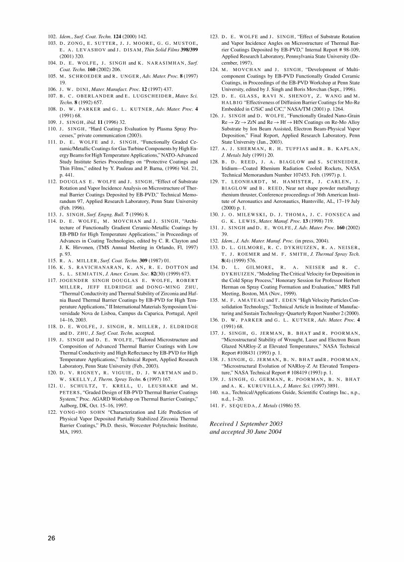
102. Idem., Surf. Coat. Techn. 124 (2000) 142.103. D . Z O N G, E . S U T T E R, J . J . M O O R E, G. G. M U S T O E,
E . A . L E V A S H O V and J . D I S A M , Thin Solid Films 398/399(2001) 320.
104. D . E . W O L F E, J . S I N G H and K. N A R A S I M H A N , Surf.Coat. Techn. 160 (2002) 206.
105. M. S C H R O E D E R and R. U N G E R , Adv. Mater. Proc. 8 (1997)19.
106. J . W. D I N I , Mater. Manufact. Proc. 12 (1997) 437.107. B . C . O B E R L A N D E R and E . L U G S C H E I D E R , Mater. Sci.
Techn. 8 (1992) 657.108. D . W. P A R K E R and G. L . K U T N E R , Adv. Mater. Proc. 4
(1991) 68.109. J . S I N G H , ibid. 11 (1996) 32.110. J . S I N G H , “Hard Coatings Evaluation by Plasma Spray Pro-
cesses,” private communication (2003).111. D . E . W O L F E and J . S I N G H , “Functionally Graded Ce-
ramic/Metallic Coatings for Gas Turbine Components by High En-ergy Beams for High Temperature Applications,” NATO-AdvancedStudy Institute Series Proceedings on “Protective Coatings andThin Films,” edited by Y. Pauleau and P. Barna, (1996) Vol. 21,p. 441.
112. D O U G L A S E. W O L F E and J . S I N G H , “Effect of SubstrateRotation and Vapor Incidence Analysis on Microstructure of Ther-mal Barrier Coatings Deposited by EB-PVD,” Technical Memo-randum 97, Applied Research Laboratory, Penn State University(Feb. 1996).
113. J . S I N G H , Surf. Engng. Bull. 7 (1996) 8.114. D . E . W O L F E, M. M O V C H A N and J . S I N G H , “Archi-
tecture of Functionally Gradient Ceramic-Metallic Coatings byEB-PBD for High Temperature Applications,” in Proceedings ofAdvances in Coating Technologies, edited by C. R. Clayton andJ. K. Hirvonen, (TMS Annual Meeting in Orlando, Fl, 1997)p. 93.
115. R . A . M I L L E R , Surf. Coat. Techn. 309 (1987) 01.116. K . S . R A V I C H A N A R A N, K. A N, R . E . D O T T O N and
S . L . S E M I A T I N , J. Amer. Ceram. Soc. 82(30) (1999) 673.117. J O G E N D E R S I N G H D O U G L A S E. W O L F E, R O B E R T
M I L L E R, J E F F E L D R I D G E and D O N G-M I N G Z H U ,“Thermal Conductivity and Thermal Stability of Zirconia and Haf-nia Based Thermal Barrier Coatings by EB-PVD for High Tem-perature Applications,” II International Materials Symposium Uni-versidade Nova de Lisboa, Campus da Caparica, Portugal, April14–16, 2003.
118. D . E . W O L F E, J . S I N G H, R . M I L L E R, J . E L D R I D G E
and D. Z H U , J. Surf. Coat. Techn. accepted.119. J . S I N G H and D. E . W O L F E , “Tailored Microstructure and
Composition of Advanced Thermal Barrier Coatings with LowThermal Conductivity and High Reflectance by EB-PVD for HighTemperature Applications,” Technical Report, Applied ResearchLaboratory, Penn State University (Feb., 2003).
120. D . V . R I G N E Y, R . V I G U I E , D . J . W A R T M A N and D.W. S K E L L Y , J. Therm. Spray Techn. 6 (1997) 167.
121. U . S C H U L T Z, T . K R E L L, U. L E U S H A K E and M.P E T E R S , “Graded Design of EB-PVD Thermal Barrier CoatingsSystem,” Proc. AGARD Workshop on Thermal Barrier Coatings,”Aalborg, DK, Oct. 15–16, 1997.
122. Y O N G-H O S O H N “Characterization and Life Prediction ofPhysical Vapor Deposited Partially Stabilized Zirconia ThermalBarrier Coatings,” Ph.D. thesis, Worcester Polytechnic Institute,MA, 1993.
123. D . E . W O L F E and J . S I N G H , “Effect of Substrate Rotationand Vapor Incidence Angles on Microstructure of Thermal Bar-rier Coatings Deposited by EB-PVD,” Internal Report # 98-109,Applied Research Laboratory, Pennsylvania State University (De-cember, 1997).
124. M. M O V C H A N and J . S I N G H , “Development of Multi-component Coatings by EB-PVD Functionally Graded CeramicCoatings, in Proceedings of the EB-PVD Workshop at Penn StateUniversity, edited by J. Singh and Boris Movchan (Sept., 1996).
125. D . E . G L A S S , R A V I N. S H E N O Y, Z . W A N G and M.H A L B I G “Effectiveness of Diffusion Barrier Coatings for Mo-ReEmbedded in C/SiC and C/C,” NASA/TM (2001) p. 1264.
126. J . S I N G H and D. W O L F E , “Functionally Graded Nano-GrainRe → Zr → ZrN and Re → Hf → HfN Coatings on Re-Mo AlloySubstrate by Ion Beam Assisted, Electron Beam-Physical VaporDeposition,” Final Report, Applied Research Laboratory, PennState University (Jan., 2003).
127. A . J . S H E R M A N, R. H. T U F F I A S and R. B . K A P L A N ,J. Metals July (1991) 20.
128. B . D . R E E D, J . A . B I A G L O W and S . S C H N E I D E R ,Iridium—Coated Rhenium Radiation Cooled Rockets, NASATechnical Memorandum Number 107453. Feb. (1997) p. 1.
129. T . L E O N H A R D T, M. H A M I S T E R, J . C A R L E N, J .B I A G L O W and B. R E E D , Near net shape powder metallurgyrhenium thruster, Conference proceedings of 36th American Insti-tute of Aeronautics and Aeronautics, Huntsville, AL, 17–19 July(2000) p. 1.
130. J . O . M I L E W S K I , D . J . T H O M A, J . C . F O N S E C A andG. K. L E W I S , Mater. Manuf. Proc. 13 (1998) 719.
131. J . S I N G H and D. E . W O L F E , J. Adv. Mater. Proc. 160 (2002)39.
132. Idem., J. Adv. Mater. Manuf. Proc. (in press, 2004).133. D . L . G I L M O R E, R . C . D Y K H U I Z E N, R . A. N E I S E R,
T . J . R O E M E R and M. F . S M I T H , J. Thermal Spray Tech.8(4) (1999) 576.
134. D . L . G I L M O R E, R . A. N E I S E R and R. C .D Y K H U I Z E N , “Modeling The Critical Velocity for Deposition inthe Cold Spray Process,” Honorary Session for Professor HerbertHerman on Spray Coating Formation and Evaluation,” MRS FallMeeting, Boston, MA (Nov., 1999).
135. M. F . A M A T E A U and T. E D E N “High Velocity Particles Con-solidation Technology,” Technical Article in Institute of Manufac-turing and Sustain Technology-Quarterly Report Number 2 (2000).
136. D . W. P A R K E R and G. L . K U T N E R , Adv. Mater. Proc. 4(1991) 68.
137. J . S I N G H, G. J E R M A N, B. B H A T and R. P O O R M A N ,“Microstructural Stability of Wrought, Laser and Electron BeamGlazed NARloy-Z at Elevated Temperatures,” NASA TechnicalReport #108431 (1993) p. 1.
138. J . S I N G H, G. J E R M A N, B. N. B H A T and R. P O O R M A N ,“Microstructural Evolution of NARloy-Z At Elevated Tempera-ture,” NASA Technical Report # 108419 (1993) p. 1.
139. J . S I N G H, G. G E R M A N, R. P O O R M A N, B. N. B H A T
and A. K. K U R U V I L L A , J. Mater. Sci. (1997) 3891.140. n.a., Technical/Applications Guide, Scientific Coatings Inc., n.p.,
n.d., 1–20.141. F . S E Q U E D A , J. Metals (1986) 55.
Received 1 September 2003and accepted 30 June 2004
26