Embed Size (px)
Citation preview

726 | J. Mater. Chem. C, 2018, 6, 726--730 This journal is©The Royal Society of Chemistry 2018
Cite this: J.Mater. Chem. C, 2018,
6, 726
Circularly polarized electroluminescence bycontrolling the emission zone in a twistedmesogenic conjugate polymer†
Jin-Hyung Jung,‡ Dong-Myung Lee,‡ Jae-Hoon Kim and Chang-Jae Yu *
This study describes the degree of circularly polarized electro-
luminescence defined by a dissymmetry g factor, depending on
the emission zone in a twisted mesogenic conjugate polymer. Using
a matrix analysis and a ratio of non-polarized emission, the emission
zone and the corresponding g factor were quantitatively analysed
without additional layers.
Introduction
The emission of polarized light from conjugated polymers withthe mesogenic phase is widely studied in both scientific interestand technical applications.1–4 In particular, the circularly polarized(CP) emission has attracted much attention in applications such asdisplays, optical information, and sensing, since the CP emissionleads to enhancement in device performance.5–8 The degree of CPemission is defined by the dissymmetry g factor g = 2(IL � IR)/(IL + IR), where IL and IR represent the intensities of left-handedCP (LHCP) light and right-handed CP (RHCP) light, respectively. Inorganic light-emitting diodes (OLEDs), the high |g| value enhancesthe luminance efficiency in an anti-reflection environment.5,6
Recently, a very high |g| value was reported in the dopedlanthanide complex. Here, the role of the position of theelectron–hole recombination (emission) zone was discussed toachieve high g factor considering the attenuation of emittedlight.9 It was theoretically expected that the g factor in aninduced twist structure of the mesogenic conjugate polymerwas varied by the emission zone using a Muller matrix analysisfor a twisted birefringent medium.6
Probing and controlling the emission zone is crucial toimprove the stability of the OLED as well as to understand thedegradation mechanism.10,11 A well-known approach towardsprobing the emission zone is to add a thin electroluminescence(EL) layer with different wavelengths at various positions within
the emitting layer (EML).11–15 However, such an approach mightbe questionable since the additional layers give rise to undesirablemotion of charge carriers within the EML. Recently, themodelling methodologies using photoluminescence (PL) andEL degradation10 or using spectrum analysis for two differentemitting materials16 were reported to determine the emissionzone. Although these approaches quantitatively described theemission zone, these methods have limitations in the applicationof various emitting materials.
In this work, we investigate the effect of position of theemission zone on the g factor in the twisted mesogenic conjugatepolymer to obtain a high g factor for enhancing the OLEDluminance. The relationship between the emission zone and theg factor was directly calculated using the Muller matrix analysis forthe continuously twisted configuration of the mesogenic conjugatepolymer. The position of the emission zone was controlled by thethickness of a hole blocking layer (HBL), which also acts as anelectron injecting hurdle (EIH). We quantitatively determined theemission zone by comparing the measured g factor and theexpected g factor associated with the emission zone. It is foundthat the g factor increases when the emission zone moves towardthe cathode but rather decreases when the emission zone entersthe HBL due to non-polarized emissions at the HBL for the thickerHBLs. Also, the penetration of the emission zone toward the HBLwas analysed with a ratio of non-polarized intensity to polarizedintensity and a peak ratio of the emissions at the EML and the HBL.
ExperimentalMaterials
For the emitting layer, the conjugate polymer, poly(9,9-di-n-octylfluorenyl-2,7-diyl)-alt-(benzo [2,1,3] thia-diazol-4,8-diyl)(F8BT) and the left-handed chiral dopant, S5011 were commerciallyacquired from Solaris Chem and Merck, respectively. The F8BTshows a nematic LC phase over 125 1C and the S5011 with a highhelical twisting power (HTP) over 100 mm�1 for small-moleculeLCs17 exhibits a HTP of about 10 mm�1 for the F8BT.6 The hole
Department of Electronic Engineering, Hanyang University, Seoul 04763,
Republic of Korea. E-mail: [email protected]
† Electronic supplementary information (ESI) available. See DOI: 10.1039/c7tc05556k‡ These authors contributed equally.
Received 4th December 2017,Accepted 22nd December 2017
DOI: 10.1039/c7tc05556k
rsc.li/materials-c
Journal ofMaterials Chemistry C
COMMUNICATION
Publ
ishe
d on
27
Dec
embe
r 20
17. D
ownl
oade
d by
Han
yang
Uni
vers
ity o
n 22
/02/
2018
00:
51:2
3.
View Article OnlineView Journal | View Issue
This journal is©The Royal Society of Chemistry 2018 J. Mater. Chem. C, 2018, 6, 726--730 | 727
blocking material, 2,20,200-(1,3,5-benzentriyl)tris(1-phenyl-1H-benzimidazole) (TPBi) and the hole injection material, copperphthalocyanine (CuPc) were commercially acquired from LUMTEC.For aligning the F8BT, the rubbed alignment layer AL22636, whichserved as the hole transport layer and the electron blocking layer,was commercially acquired from Japan Synthetic Rubber. Allmaterials were used directly without further purification. Thechemical structures of the used materials are shown in Fig. 1a.
Device fabrication
The OLEDs with various thicknesses of the TPBi on the S5011-doped F8BT layer were fabricated in this work. The devicestructures and energy levels are illustrated in Fig. 1b. Prepatternedindium-tin-oxide (ITO) substrates (a sheet resistance E20 O &�1)were cleaned by ultrasonication in deionized water and mucasol(alkali detergent) for 60 min. The CuPc, served as a holeinjection layer, with a thickness of 2 nm was deposited bythermal evaporation under a vacuum of 6 � 10�6 Torr on theITO surface. To align the EML, the AL22636 was spin-coated (at1000 rpm for 10 s and 3000 rpm for 20 s) on the CuPc andunidirectionally rubbed by a rubbing machine after imidizingthe alignment layer via baking at 210 1C for 60 min. The rubbingmachine consists of a 6.5 cm-diameter roller covered with acotton cloth. The rotational speed of the roller and the transla-tional speed of the substrate stage were fixed at 500 rpm and6 mm s�1, respectively.18 The dissolved F8BT mixture blendedwith 7 wt% S5011 in toluene (25.11 mg mL�1) was spin-coated(at 1000 rpm for 10 s and 3000 rpm for 20 s) on the rubbedAL22636 and baked at 150 1C for 10 min (the thickness of theF8BT is 120 nm). The total twisted angle of the F8BT layer wasevaluated to be 861 (see the ESI†). TPBi with various thicknesses(0, 10, 20, 30, 40, and 50 nm), LiF (1 nm), and Al (70 nm) were
sequentially deposited by thermal evaporation. All samples wereencapsulated by glass and UV curable resin (NOA 65 formNorland Products) under a nitrogen atmosphere to avoid exposureto oxygen and humidity.
Device characterization
The linearly polarized photoluminescence (LPPL) and the CPelectroluminescence (CPEL) of the OLEDs were measured usinga spectroradiometer (TOPCON, SR-UL 1R) under a rotary stage.The birefringence of the F8BT was measured using the photo-elastic modulator (PEM) (Hinds, PEM-100) and the lock-inamplifier (Stanford Research System, SR830) based on thePEM method (see the ESI†). The LPPL was measured using theintensity ratio of the parallel component to the aligned direction ofthe F8BT to the perpendicular one. The CPEL was observed under acircular polarizer consisting of a linear polarizer and a quarter-wave-plate (QWP) for 546 nm. Two orthogonal CPELs were measured byrotating the QWP by �451 with respect to the linear polarizer.All measurements were carried out in ambient environmentsafter encapsulation.
Results and discussionLPPL characteristics
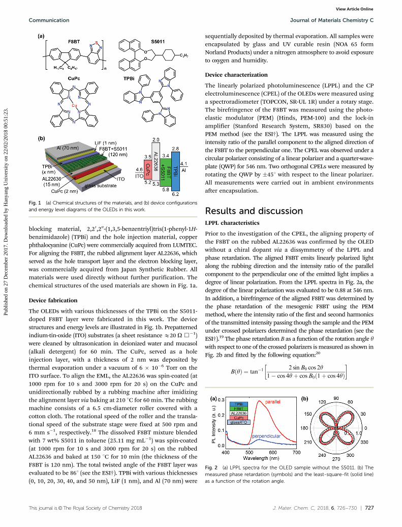
Prior to the investigation of the CPEL, the aligning property ofthe F8BT on the rubbed AL22636 was confirmed by the OLEDwithout a chiral dopant via a dissymmetry of the LPPL andphase retardation. The aligned F8BT emits linearly polarized lightalong the rubbing direction and the intensity ratio of the parallelcomponent to the perpendicular one of the emitted light implies adegree of linear polarization. From the LPPL spectra in Fig. 2a, thedegree of the linear polarization was evaluated to be 0.88 at 546 nm.In addition, a birefringence of the aligned F8BT was determined bythe phase retardation of the mesogenic F8BT using the PEMmethod, where the intensity ratio of the first and second harmonicsof the transmitted intensity passing though the sample and the PEMunder crossed polarizers determined the phase retardation (see theESI†).19 The phase retardation B as a function of the rotation angle ywith respect to one of the crossed polarizers is measured as shown inFig. 2b and fitted by the following equation:20
BðyÞ ¼ tan�12 sinB0 cos 2y
1� cos 4yþ cosB0ð1þ cos 4yÞ
� �
Fig. 1 (a) Chemical structures of the materials, and (b) device configurationsand energy level diagrams of the OLEDs in this work.
Fig. 2 (a) LPPL spectra for the OLED sample without the S5011. (b) Themeasured phase retardation (symbols) and the least-square-fit (solid line)as a function of the rotation angle.
Communication Journal of Materials Chemistry C
Publ
ishe
d on
27
Dec
embe
r 20
17. D
ownl
oade
d by
Han
yang
Uni
vers
ity o
n 22
/02/
2018
00:
51:2
3.
View Article Online
728 | J. Mater. Chem. C, 2018, 6, 726--730 This journal is©The Royal Society of Chemistry 2018
Here, B0 (= 2pDnd/l) is an effective phase retardation of a thin filmwith thickness d and birefringence Dn at wavelength l. It shouldbe noted that the phase retardation, induced by the alignmentlayer and the TPBi layer, is negligible. The birefringence of theF8BT was 0.67 at 546 nm. The degree of the linear polarization andthe birefringence are necessary to evaluate the dissymmetry gfactor of the CPEL.
CPEL characteristics
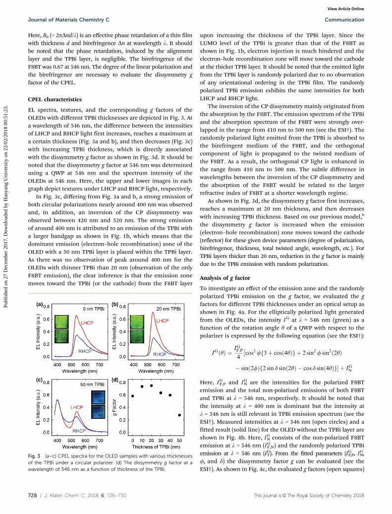
EL spectra, textures, and the corresponding g factors of theOLEDs with different TPBi thicknesses are depicted in Fig. 3. Ata wavelength of 546 nm, the difference between the intensitiesof LHCP and RHCP light first increases, reaches a maximum ata certain thickness (Fig. 3a and b), and then decreases (Fig. 3c)with increasing TPBi thickness, which is directly associatedwith the dissymmetry g factor as shown in Fig. 3d. It should benoted that the dissymmetry g factor at 546 nm was determinedusing a QWP at 546 nm and the spectrum intensity of theOLEDs at 546 nm. Here, the upper and lower images in eachgraph depict textures under LHCP and RHCP light, respectively.
In Fig. 3c, differing from Fig. 3a and b, a strong emission ofboth circular polarizations nearly around 400 nm was observedand, in addition, an inversion of the CP dissymmetry wasobserved between 420 nm and 520 nm. The strong emissionof around 400 nm is attributed to an emission of the TPBi witha larger bandgap as shown in Fig. 1b, which means that thedominant emission (electron–hole recombination) zone of theOLED with a 50 nm TPBi layer is placed within the TPBi layer.As there was no observation of peak around 400 nm for theOLEDs with thinner TPBi than 20 nm (observation of the onlyF8BT emission), the clear inference is that the emission zonemoves toward the TPBi (or the cathode) from the F8BT layer
upon increasing the thickness of the TPBi layer. Since theLUMO level of the TPBi is greater than that of the F8BT asshown in Fig. 1b, electron injection is much hindered and theelectron–hole recombination zone will move toward the cathodeat the thicker TPBi layer. It should be noted that the emitted lightfrom the TPBi layer is randomly polarized due to no observationof any orientational ordering in the TPBi film. The randomlypolarized TPBi emission exhibits the same intensities for bothLHCP and RHCP light.
The inversion of the CP dissymmetry mainly originated fromthe absorption by the F8BT. The emission spectrum of the TPBiand the absorption spectrum of the F8BT were strongly over-lapped in the range from 410 nm to 500 nm (see the ESI†). Therandomly polarized light emitted from the TPBi is absorbed tothe birefringent medium of the F8BT, and the orthogonalcomponent of light is propagated to the twisted medium ofthe F8BT. As a result, the orthogonal CP light is enhanced inthe range from 410 nm to 500 nm. The subtle difference inwavelengths between the inversion of the CP dissymmetry andthe absorption of the F8BT would be related to the largerrefractive index of F8BT at a shorter wavelength regime.
As shown in Fig. 3d, the dissymmetry g factor first increases,reaches a maximum at 20 nm thickness, and then decreaseswith increasing TPBi thickness. Based on our previous model,6
the dissymmetry g factor is increased when the emission(electron–hole recombination) zone moves toward the cathode(reflector) for these given device parameters (degree of polarization,birefringence, thickness, total twisted angle, wavelength, etc.). ForTPBi layers thicker than 20 nm, reduction in the g factor is mainlydue to the TPBi emission with random polarization.
Analysis of g factor
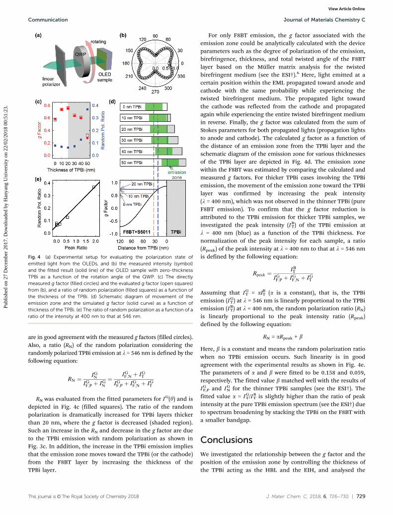
To investigate an effect of the emission zone and the randomlypolarized TPBi emission on the g factor, we evaluated the gfactors for different TPBi thicknesses under an optical setup asshown in Fig. 4a. For the elliptically polarized light generatedfrom the OLEDs, the intensity I G at l = 546 nm (green) as afunction of the rotation angle y of a QWP with respect to thepolarizer is expressed by the following equation (see the ESI†):
IGðyÞ ¼IGF;P4
cos2 ff3þ cosð4yÞg þ 2 sin2 f sin2ð2yÞ�
� sinð2fÞf2 sin d sinð2yÞ � cos d sinð4yÞg� þ IGN
Here, I GF,P and I G
N are the intensities for the polarized F8BTemission and the total non-polarized emissions of both F8BTand TPBi at l = 546 nm, respectively. It should be noted thatthe intensity at l = 400 nm is dominant but the intensity atl = 546 nm is still relevant in TPBi emission spectrum (see theESI†). Measured intensities at l = 546 nm (open circles) and afitted result (solid line) for the OLED without the TPBi layer areshown in Fig. 4b. Here, I G
N consists of the non-polarized F8BTemission at l = 546 nm (I G
F,N) and the randomly polarized TPBiemission at l = 546 nm (IG
T). From the fitted parameters (IGF,P, IG
N,f, and d) the dissymmetry factor g can be evaluated (see theESI†). As shown in Fig. 4c, the evaluated g factors (open squares)
Fig. 3 (a–c) CPEL spectra for the OLED samples with various thicknessesof the TPBi under a circular polarizer. (d) The dissymmetry g factor at awavelength of 546 nm as a function of thickness of the TPBi.
Journal of Materials Chemistry C Communication
Publ
ishe
d on
27
Dec
embe
r 20
17. D
ownl
oade
d by
Han
yang
Uni
vers
ity o
n 22
/02/
2018
00:
51:2
3.
View Article Online
This journal is©The Royal Society of Chemistry 2018 J. Mater. Chem. C, 2018, 6, 726--730 | 729
are in good agreement with the measured g factors (filled circles).Also, a ratio (RN) of the random polarization considering therandomly polarized TPBi emission at l = 546 nm is defined by thefollowing equation:
RN ¼IGN
IGF;P þ IGN¼
IGF;N þ IGT
IGF;P þ IGF;N þ IGT
RN was evaluated from the fitted parameters for I G(y) and isdepicted in Fig. 4c (filled squares). The ratio of the randompolarization is dramatically increased for TPBi layers thickerthan 20 nm, where the g factor is decreased (shaded region).Such an increase in the RN and decrease in the g factor are dueto the TPBi emission with random polarization as shown inFig. 3c. In addition, the increase in the TPBi emission impliesthat the emission zone moves toward the TPBi (or the cathode)from the F8BT layer by increasing the thickness of theTPBi layer.
For only F8BT emission, the g factor associated with theemission zone could be analytically calculated with the deviceparameters such as the degree of polarization of the emission,birefringence, thickness, and total twisted angle of the F8BTlayer based on the Muller matrix analysis for the twistedbirefringent medium (see the ESI†).6 Here, light emitted at acertain position within the EML propagated toward anode andcathode with the same probability while experiencing thetwisted birefringent medium. The propagated light towardthe cathode was reflected from the cathode and propagatedagain while experiencing the entire twisted birefringent mediumin reverse. Finally, the g factor was calculated from the sum ofStokes parameters for both propagated lights (propagation lightsto anode and cathode). The calculated g factor as a function ofthe distance of an emission zone from the TPBi layer and theschematic diagram of the emission zone for various thicknessesof the TPBi layer are depicted in Fig. 4d. The emission zonewithin the F8BT was estimated by comparing the calculated andmeasured g factors. For thicker TPBi cases involving the TPBiemission, the movement of the emission zone toward the TPBilayer was confirmed by increasing the peak intensity(l = 400 nm), which was not observed in the thinner TPBi (pureF8BT emission). To confirm that the g factor reduction isattributed to the TPBi emission for thicker TPBi samples, weinvestigated the peak intensity (I B
T) of the TPBi emission atl = 400 nm (blue) as a function of the TPBi thickness. Fornormalization of the peak intensity for each sample, a ratio(Rpeak) of the peak intensity at l = 400 nm to that at l = 546 nmis defined by the following equation:
Rpeak ¼IBT
IGF;P þ IGF;N þ IGT
Assuming that I GT = aIB
T (a is a constant), that is, the TPBiemission (I G
T) at l = 546 nm is linearly proportional to the TPBiemission (I B
T) at l = 400 nm, the random polarization ratio (RN)is linearly proportional to the peak intensity ratio (Rpeak)defined by the following equation:
RN = aRpeak + b
Here, b is a constant and means the random polarization ratiowhen no TPBi emission occurs. Such linearity is in goodagreement with the experimental results as shown in Fig. 4e.The parameters of a and b were fitted to be 0.158 and 0.059,respectively. The fitted value b matched well with the results ofI G
F,P and I GN for the thinner TPBi samples (see the ESI†). The
fitted value a = I GT/I B
T is slightly higher than the ratio of peakintensity at the pure TPBi emission spectrum (see the ESI†) dueto spectrum broadening by stacking the TPBi on the F8BT witha smaller bandgap.
Conclusions
We investigated the relationship between the g factor and theposition of the emission zone by controlling the thickness ofthe TPBi acting as the HBL and the EIH, and analysed the
Fig. 4 (a) Experimental setup for evaluating the polarization state ofemitted light from the OLEDs, and (b) the measured intensity (symbol)and the fitted result (solid line) of the OLED sample with zero-thicknessTPBi as a function of the rotation angle of the QWP. (c) The directlymeasured g factor (filled circles) and the evaluated g factor (open squares)from (b), and a ratio of random polarization (filled squares) as a function ofthe thickness of the TPBi. (d) Schematic diagram of movement of theemission zone and the simulated g factor (solid curve) as a function ofthickness of the TPBi. (e) The ratio of random polarization as a function of aratio of the intensity at 400 nm to that at 546 nm.
Communication Journal of Materials Chemistry C
Publ
ishe
d on
27
Dec
embe
r 20
17. D
ownl
oade
d by
Han
yang
Uni
vers
ity o
n 22
/02/
2018
00:
51:2
3.
View Article Online
730 | J. Mater. Chem. C, 2018, 6, 726--730 This journal is©The Royal Society of Chemistry 2018
Muller matrix analysis. For the polarized EML emission, the gfactor increased when the emission zone moved toward thecathode upon increasing the TPBi thickness. However, the TPBiemission was observed and the g factor was reduced in thickerTPBi cases. The reduction in the g factor was due to the non-polarized TPBi emission and was quantitatively expressed withthe ratio of non-polarized intensity to polarized one and thepeak ratio of the emissions at the EML and the TPBi. Thisapproach opens a new door to improve the g factor (enhancethe OLED luminance in anti-reflection environments) for agiven EML and to directly probe the emission zone with noadditional layer and no performance degradation.
Conflicts of interest
There are no conflicts of interest to declare.
Acknowledgements
This work is supported by the KDRC (Korea Display ResearchConsortium) support program for the development of futuredevice technologies for display industry.
Notes and references
1 M. Jandke, P. Strohriegl, J. Gmeiner, W. Brutting andM. Schwoerer, Adv. Mater., 1999, 11, 1518–1521.
2 U. Mitschke and P. Bauerle, J. Mater. Chem., 2000, 10, 1471–1507.3 M. O’Neill and S. M. Kelly, Adv. Mater., 2011, 23, 566–584.4 D.-M. Lee, Y.-J. Lee, J.-H. Kim and C.-J. Yu, Opt. Express,
2017, 25, 3737–3742.
5 R. Singh, K. N. N. Unni, A. Solanki and Deepak, Opt. Mater.,2012, 34, 716–723.
6 D.-M. Lee, J.-W. Song, Y.-J. Lee, C.-J. Yu and J.-H. Kim, Adv.Mater., 2017, 29, 1700907.
7 C. Wagenknecht, C.-M. Li, A. Reingruber, X.-H. Bao,A. Goebel, Y.-A. Chen, Q. Zhang, K. Chen and J.-W. Pan,Nat. Photonics, 2010, 4, 549–552.
8 Y. Yang, R. C. da Costa, M. J. Fuchter and A. J. Campbell,Nat. Photonics, 2013, 7, 634–638.
9 F. Zinna, M. Pasini, F. Galeotti, C. Botta, L. D. Bari andU. Giovanella, Adv. Funct. Mater., 2017, 27, 1603719.
10 C. Peng, A. Salehi, Y. Chen, M. Danz, G. Liaptsis and F. So,ACS Appl. Mater. Interfaces, 2017, 9, 41421–41427.
11 Y. Zhang, J. Lee and S. R. Forrest, Nat. Commun., 2014,5, 5008.
12 C. Coburn, J. Lee and S. R. Forrest, Adv. Opt. Mater., 2016, 4,889–895.
13 W. Song, W. Lee, K. K. Kim and J. Y. Lee, Org. Electron.,2016, 37, 252–256.
14 U. S. Bhansali, H. Jia, M. A. Q. Lopez, B. E. Gnade,W.-H. Chen and M. A. Omary, Appl. Phys. Lett., 2009,94, 203501.
15 K. S. Yook and J. Y. Lee, J. Ind. Eng. Chem., 2010, 16, 181–184.16 M. C. Gather, M. Flammich, N. Danz, D. Michaelis and
K. Meerholz, Appl. Phys. Lett., 2009, 94, 263301.17 Y. Chen and S.-T. Wu, J. Appl. Polym. Sci., 2014, 131, 40556.18 S. I. Jo, Y. Kim, J.-H. Baek, C.-J. Yu and J.-H. Kim, Jpn. J. Appl.
Phys., 2014, 53, 03CD04.19 Hinds Instruments, PEM-100 Technical Note.20 J.-H. Lee, C.-J. Yu and S.-D. Lee, Mol. Cryst. Liq. Cryst., 1998,
321, 317–322.
Journal of Materials Chemistry C Communication
Publ
ishe
d on
27
Dec
embe
r 20
17. D
ownl
oade
d by
Han
yang
Uni
vers
ity o
n 22
/02/
2018
00:
51:2
3.
View Article Online