Embed Size (px)
Citation preview

Adaptation to scientific and technological progress under Directive 2002/95/EC
Joint response from EICTA, AeA Europe, EECA ESIA and ZVEI to the general and specific questionnaires
relating to Exemption 7.c: Lead in electronic ceramic parts (e.g. piezoelectronic devices)
31 March 2008
Content General questionnaire p.2 Specific questionnaire p. 16 Annexes : I – Applications of PZT in EEE p. 19
II - Data / evidence on why substitution is impracticable p. 20
Page 1 of 21

Page 2 of 21
General questionnaire 1. For which substance(s) or compound(s) should the requested exemption be valid?
Lead in electronic ceramic parts. Three electronic ceramics parts contains lead: 1- Piezoelectric ceramics (PZT):
o Also known as Lead Zirconate Titanate (PZT) ceramics o Ceramics consisting of a mixture of PbZrO3 and PbTiO3. Piezoelectric ceramics generate an electrical charge
when mechanically loaded with pressure, tension, acceleration. This effect is the direct piezo effect. The polarity of the charge depends on the orientation of the crystals in the piezo ceramic relative to the direction of the pressure. Conversely, the crystals in piezo ceramics undergo a controlled deformation when exposed to an electrical field – a behaviour referred to as the inverse piezo effect. Piezoelectric ceramics contain lead as high covalent compound in the ceramic matrix to achieve good ferroelectric properties over a wide temperature range.
2- Positive Temperature Coefficient (PTC): Materials increasing their electrical resistance with increasing temperature; as PTC ceramics (Positive Temperature Coefficient) used in PTC resistors or PTC thermistors. PTC ceramics is the description of an electrical material functionality which is used for overload protection in high voltage electric circuits. Usually PTC resistors are based on polycrystalline barium titanate which becomes semi-conductive by doping with further metallic oxides. The lead content within these materials is about 4% -14% by weight. PTC ceramics increase their electrical resistance with increasing temperature. Lead is also indispensable for these ceramics to achieve the required resistance-voltage characteristics and distribution of the resistance value. 3- Dielectric ceramics: a. Ceramic capacitors - General: Dielectric ceramic is the basis for ceramic capacitors. b. Ceramic capacitors - High K / High power: Ceramic capacitors with high capacitance values for high voltage / high power applications need a lead based ceramic. High K Ceramics based on barium titanate and strontium titanate are not suitable because of too high losses and self heating. The lead content of High K / High power ceramics is about 50% by weight.
2. What is the application in which the substance/compound is used for and what is its specific technical function?
1- Piezoelectric ceramics (PZT): o Examples for products using PZT: Motor vehicles, PCs, mobile phones, inkjet printers, hard disks, video
recorders, video games, audio equipment, air conditioners, refrigerators, washing machines, smoke detectors, health measurement equipment, trains, helicopters, skis, endoscopes, soundproof walls.
o Examples for components using PZT: Focus/zoom of mobile phones, power supply transformers (PCs), print heads, precision alignment of optical fibers, active rotor blades for helicopters, various active dampers, micro-positioners, medical injections, automotive injection, noise canceling, magnetic sensors.
o Examples for applications: Oscillator, filter, buzzer, sensor, phonating, actuator, print head, stabilizer, transformer, inverter, pump. PZT ceramics are also used in transducers, and function as a piezoelectric

Page 3 of 21
material. 2- Positive Temperature Coefficient (PTC):
o Applications: overheat prevention (personal computer, LCD TV/PDP TV, power supply), current control (energy saving light system, compact fluorescent lamp), overcurrent protection (telephone, measuring equipment).
3- Dielectric ceramics: Dielectric ceramics are generally applied to store energy in electrical and electronic devices or parts thereof: - Electrical and electronic control circuits; - Ceramic capacitors for high power (exceeding DC 250 V and AC 125 V);
o - HID (high intensity discharge) lamps. 3. What is the specific (technical) function of the substance/compound in this application?
1- Piezoelectric ceramics (PZT): Piezoelectric ceramics contain lead as high covalent compound in the ceramic matrix to achieve good ferroelectric properties in a wide temperature range. The best known performances can be reached with PZT ceramics, which are a mixture of PbTiO3 and PbZrO3. The lead content is between 58% and 68% by weight, depending on the proportion of zirconium (Zr) and titanium (Ti). 2- Positive Temperature Coefficient (PTC): PTC ceramics (Positive Temperature Coefficient) is the description of an electrical material functionality which is used for overload protection in high voltage electric circuits. Usually PTC resistors are based on polycrystalline barium titanate which becomes semi-conductive by doping with further metallic oxides. The lead content within these materials is about 4% -14% by weight. 3- Dielectric ceramics: Dielectric ceramic is the basis for ceramic capacitors. Ceramic capacitors with high capacitance values for high voltage / high power applications need a lead based ceramic. The ceramics are based on barium titanate and strontium titanate are not suitable because of too high losses and self heating. The lead content of these ceramics is about 50% by weight.
4. Please justify why this application falls under the scope of the RoHS Directive (e.g. is it a finished product?
Electronic components mentioned in 2 above do not fall directly under the scope of RoHS themselves, but become parts of products that are under RoHS. Those components, however, are used within EEE according to the scope of RoHS.
- Is it a fixed installation?
Yes, in some cases. These parts are also used in applications outside of fixed installations.
- What category of the WEEE Directive does it belong to?).
EICTA products for this exemption would fall under category 3 (IT and telecommunications equipment) and category 4 (consumer equipment). Furthermore, the capacitors, resistors and other components that use this exemption are used in a wide array of consumer and electronic goods covered by other categories. They are assembled into semiconductor Land Grid Array (LGA) packages and complex module packages. While these semiconductors may be used for many EEE

Page 4 of 21
applications, they are commonly used for Radio Frequency (RF) products and sensors. 5. What is the amount (in absolute number and in percentage by weight) of the substance/compound in:
i) the homogeneous material
PZT: in average between 55% to 85% wt in compound.
ii) the application, and Semiconductors may contain capacitors, resistors and other components that require this exemption for lead in ceramics. Individual amounts will vary based on the number of exempt components used per semiconductor package. When incorporating these exempt components, semiconductor packages may contain between 0.0000003 and 0.013 grams of lead, with a general average of 0.00013 grams. This lead concentration represents 0.0002% to 0.104% of any single semiconductor component, with an average of 0.034% lead for the 2% of products that use this exemption. 0,0001300 Pb gs / unit (ceramics) = 0.13 mgs/unit
iii) total EU annually for RoHS relevant applications?
Information to be provided by our suppliers later.
6. Please check and justify why the application you request an exemption for does not overlap with already existing exemptions respectively does not overlap with exemption requests covered by previous consultations.
Not applicable – this is only for new exemption requests
7. Please provide an unambiguous wording for the (requested) exemption.
Lead in electronic ceramic parts (e.g. piezoeletronic devices). EICTA suggests that the Oko Institut to follow the recommendations of the final report on the revision of the exemptions of the ELV Directive. Published on 16 January 2008, the final report states that ‘The stakeholders decided that the current exemption wording covers all their relevant uses of lead in ceramics. It is hence recommended to continue the exemption with the current wording.’
8. Please justify your contribution according to Article 5 (1) (b) RoHS Directive whereas:
Under the stakeholder consultation on the revision of ELV exemptions, JEITA provided the Oko Institut with an article on research and development activities from industry on possible alternatives to lead in electronic ceramic parts. Possible alternatives exist such as bismuth sodium titanate, bismuth layers, and others. Nevertheless, research is not advanced enough to allow industry to use these alternatives for mass production of lead-free electronic ceramic parts. This document is available on the Circa website, under the specific section to the ELV Directive revision:

Page 5 of 21
http://circa.europa.eu/Public/irc/env/elv/library?l=/stakeholder_consultation/request_exemption/electrical_components/comments_of_jeita/ceramicmaterials_2/_EN_1.0_&a=d

Page 6 of 21
o Substitution of concerned hazardous substances via materials and components not containing these is technically or scientifically either practicable or impracticable;
1- Piezoelectric ceramics (PZT): It is technically and scientifically impracticable. The relationship between Curie temperature and the constant of piezoelectric material is important in applying the piezoelectric effect. Please find an example of the piezoelectric material constant below:
Piezoelectric Strain Coefficient (d constant)
If the value is high, it can generate displacement efficiently from a low electric field. Also, it makes the output larger for sensors and it can be used as good sensor material with high sensitivity
Electro Mechanical Coupling Coefficient
Coefficient to show the efficiency to transform and communicate electric alteration into the energy of mechanical alteration (or vice versa) due to the piezoelectric effect. In order to gain filter characteristics, materials with high values in this category are essential.
Mechanical Quality Factor Coefficient to show the extent of mechanical loss near frequencies where the piezoelectric substance resonates. In resonators and oscillators, as the value becomes higher, the oscillator becomes more efficient and the fluctuation in the resonance frequency decreases.
We also find a piezoelectric effect in Barium titanate, although it lacks the characteristics of the piezoelectric material constant, applied in actuators, sensors, oscillators, filters and transformers etc. As a result we obtain the intended piezoelectric effect by incorporating lead into the crystal structure of ceramics to change the characteristics and by obtaining high performance coefficient of piezoelectric materials such as Curie temperature etc As mentioned above, the piezoelectric material constant required for piezoelectric ceramic is the minimum required characteristic for application in electrical products application. This means that if this ceramic feature is not obtained, the application is not valid (example: it does not function as a filter or actuator). As it is not valid as application of piezoelectric ceramics, it does not make sense to lower the values of required specifications or standards. We acknowledge that several materials, such as titanate niobium, showing the piezoelectric effect are being recommended as substitute materials. However, even if these features of these ceramics are obtained on a mass-production scale, they can only be substituted in limited piezoelectric applications. Besides, according to the currently released report, the mass-production technology is not established and how to maintain the scheduled piezoelectric effect stably remains to be worked out.

Page 7 of 21
2- Positive Temperature Coefficient (PTC): Please refer to JEITA answers to the questionnaire on exemption 7.c. 3- Dielectric ceramics: Currently, it is technically and scientifically impracticable. Nevertheless, in near future, it will be practicable only for low voltage capacitors. Some of these electronic components which use dielectric ceramics, no longer use material containing lead. For the remaining electronic components that use dielectric ceramics containing lead, there are potential substitutes. It is expected that the substitution can be promoted by appropriately setting the timing for development, evaluation and substitution of application. There is no substitute for materials used in high voltage capacitors among the lead-containing dielectric ceramics and no appropriate shifter other than lead has been proposed. Some people have proposed the use of Barium titanate as a potential substitute material. However, it has the characteristic of being likely to distort when voltage is imposed and the lack of strength is a concern in the application of electronic components which are used under high voltage. In order to obtain the function to withstand high voltage and to accumulate a large amount of electricity, a material which loses a small amount of accumulated electricity is required. Strontium titanate is appropriate for this. However, strontium titanate has a poor ability to accumulate electricity at room temperature. Thus, we ensure the ability to accumulate electricity containing the accumulated electric loss by adding lead as a shifter. Therefore there is no prospect of substitution of high voltage capacitors at the moment. Even capacitors comprised of dielectric substance other than ceramics cannot ensure a similar function. The function of high voltage capacitors is guaranteed in safety standards and if we push for substitution, it is possible that functions to be guaranteed in safety standards will not guaranteed.
o Elimination or substitution of concerned hazardous substances via design changes is technically or scientifically either practicable or impracticable;
Substitution of lead electronic ceramic parts via design changes is scientifically and technically impracticable at this moment. Please refer to JEITA contribution on exemption 7.c.

Page 8 of 21
o Negative environmental, health and/or consumer safety impacts caused by substitution are either likely or unlikely to outweigh environmental, health and/or consumer safety benefits thereof (If existing, please refer to relevant studies on negative or positive impacts caused by substitution).
1- Environmental impact of substitutes linked to manufacturing and refinement : In March 2004, the Eco Material Center of the National Institute for Material Science in Japan published a report on the efficient use of resources and their influence on environment during the entire lifetime of the substance and material cycle. This report quantifies the environmental impacts of various metals with an index of “Total Materials Requirement (TMR)”. The Total Materials Requirement (TMR) refers to the total amount of global resources involved in production. The report is only available in Japanese on the following website: http://www.lifecycle.jp/manual/coefficient_of_resources.pdf (Please see p.26). According to this report, bismuth and niobium indicated as a substitute material for lead are estimated to have a larger environmental impact due to their scarcity. Comparison of TMR between lead and potential substitutes:
lead 95 (comparative criterion) bismuth 150,000 (approximately 1500 times) niobium 1,400 (approximately 14 times)
Given that bismuth is obtained as a by-product of lead ore, lead would be produced anyway if industry substitutes it by bismuth. Therefore, the environmental impacts of bismuth are even higher than expected due to the amount of energy required to produce bismuth from lead. 2- Environmental impact of substitutes linked to the use phase:
A) Piezoelectric transformers
Based on the principle of piezoelectric transformers, the mechanical vibration is the resonance and it generates heat in parts which are joined. The heat alters the electric characteristics such as dielectric constant increasing the energy loss. Therefore, it is necessary that the mechanical quality coefficient (Qm) is high, that dielectric loss is small (tanδ), and that the electromechanical coupling coefficient (kp) is large for the material. If Qm is high, the deterioration of vibration becomes small and if tanδ is small, the thermal loss of electric energy is restrained and if kp is large, the conversion efficiency of electric energy and mechanical vibration energy becomes large, decreasing energy loss. If we compare the characteristic value of Qm and tanδ for non lead-based material and lead-based material (conventional products), in non lead-based material the Qm is smaller and the tanδ is larger than conventional products as shown in Figure 1. If it is used as a piezoelectric transformer, the generated heat is larger than conventional products with larger deterioration of characteristics and energy loss.

Page 9 of 21
Figure 2 shows the comparison result of Qm and kp. As mentioned previously, non lead-based material has a larger deviation than current material and in order to obtain similar characteristics, larger energy will be needed which increases the environmental load as a result.
0
500
1000
1500
2000
2500
3000
3500
0 3 4
●,●,●:
鉛系圧電材料
Figure 1: Technology map of piezoelectric ceramics from the aspect of tanδ and Qm
1 2
損失係数 tanδ(%)
機械的品質係数 Qm
● :非鉛系圧電材料
アクチュエータ、音響、センサ
振動子、広帯域フィル タ、トランス
Mechanical quality coefficient Qm
Actuators, Acoustic, Sensors
Oscillators, Broad-band filters Transformers
: Lead-based piezoelectric material : Non lead-based piezoelectric material
Loss coefficient tanδ (%)
0
500
1000
1500
2000
2500
3000
3500
0 10 20 30 40 50 60 70 80 90 100
電気機械結合係数 Kp(%)
機械的品質係数 Qm
●,●,●:
鉛系圧電材料● :非鉛系圧電材料
アクチュエータ、音響、センサ
: Lead-based piezoelectric material : Non lead-based piezoelectric Mechanical
振 ス動子、広帯域フィル タ、トラン
Electromechanical coupling coefficient Kp(%)
Oscillators, Broad-band filters, Transformers
q
Actuators, Acoustic, S
uality
Figure 2: Technology map of piezoelectric ceramics from the aspect of Kp and
Page 10 of 21
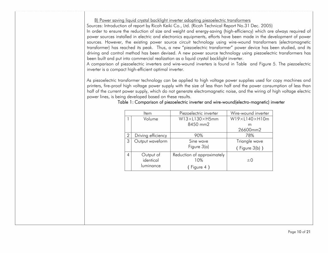
B) Power saving liquid crystal backlight inverter adopting piezoelectric transformers
Sources: Introduction of report by Ricoh Keiki Co., Ltd. (Ricoh Technical Report No.31�Dec. 2005) In order to ensure the reduction of size and weight and energy-saving (high-efficiency) which are always required of power sources installed in electric and electronics equipments, efforts have been made in the development of power sources. However, the existing power source circuit technology using wire-wound transformers (electromagnetic transformer) has reached its peak. Thus, a new “piezoelectric transformer” power device has been studied, and its driving and control method has been devised. A new power source technology using piezoelectric transformers has been built and put into commercial realization as a liquid crystal backlight inverter. A comparison of piezoelectric inverters and wire-wound inverters is found in Table�and Figure 5. The piezoelectric inverter is a compact high-efficient optimal inverter. As piezoelectric transformer technology can be applied to high voltage power supplies used for copy machines and printers, fire-proof high voltage power supply with the size of less than half and the power consumption of less than half of the current power supply, which do not generate electromagnetic noise, and the wiring of high voltage electric power lines, is being developed based on these results.
Table 1: Comparison of piezoelectric inverter and wire-wound(electro-magnetic) inverter
Item Piezoelectric inverter Wire-wound inverter 1 Volume W13×L130×H5mm
8450 mm2 W19×L140×H10m
m 26600mm2
2 Driving efficiency 90% 78% 3 Output waveform Sine wave
�Figure 3(a)� Triangle wave
(Figure 3(b)) 4 Output of
identical luminance
Reduction of approximately 10%
(Figure 4)
±0

C) Dielectric ceramics Barium titanate, which is normally used as a material for ceramic capacitors, is available as a non-lead dielectric ceramic. However, the loss is many orders of magnitude larger than the current lead-containing ceramics and becomes unstable at generating high heat when high voltage is imposed. Since barium titanate has the tendency to get distorted when voltage is imposed (electrostrictive strain property), it generates mechanical breakdown when high voltage impact is added and cannot be used. Strontium titanate is available as a non-lead dielectric ceramic without electrostrictive strain property with a small amount of loss. However, the dielectric constant is as small as one twelfth of the current lead-based material. Thus it becomes as large as ten times the current size if we are to make a high-voltage capacitor with it.
(b) (a)
Figure 3: Output waveform of inverters (a) Piezoelectric INV, (b) Electromagnetic INV
Page 11 of 21
Figure 4: Relationship of input electricity and output voltage (TFT14inch luminance 100cd/m2 h)
Piezoelectric INV
Electromagnetic INV
3-b-図6 特性の総合評価
省電力
輝度効率
電磁ノイズ
形状
価格
安全性
Electromagnetic noise
Luminance efficiency
Energy saving
Piezoelectric inverter vs wire-wound inverter
Safety
Piezoelectric inverter Wire-wound inverter
Price
Form
Figure 5: Comprehensive evaluation of characteristics

As mentioned above, non lead-based materials are not practical because we cannot impose high-voltage or the size becomes too large from the point of characteristics such as heat and damage. This means that the realization of current applications becomes impossible and the environmental load will be large as a result.
As explained through our answers to questions 8a and 8b, we should not discuss focusing on the harmfulness of lead but find a measure which is friendly to environment and has a lower impact on the environment. 3- Summary of the environmental impact of substitutes:
A) Obtaining the premium grade material used as substitute materials for lead will increase the energy used and
conversely may increase the impact on the environment. Example 1: Bismuth and other products are obtained as by-products of lead. To obtain bismuth, the unwanted lead from mining and refining lead ore must be disposed of properly. Example 2: When using niobium and other scarce resources that are unevenly distributed around the world, resource depletion and the energy used for mining and transporting the products increases. There is also the concern that supplies will be unstable.
B) If substitute metals are introduced, the quantities of devices, components and materials containing lead requiring disposal will be very significant for some time.
9. Please provide sound data/evidence on why substitution / elimination is either practicable or impracticable (e.g. what
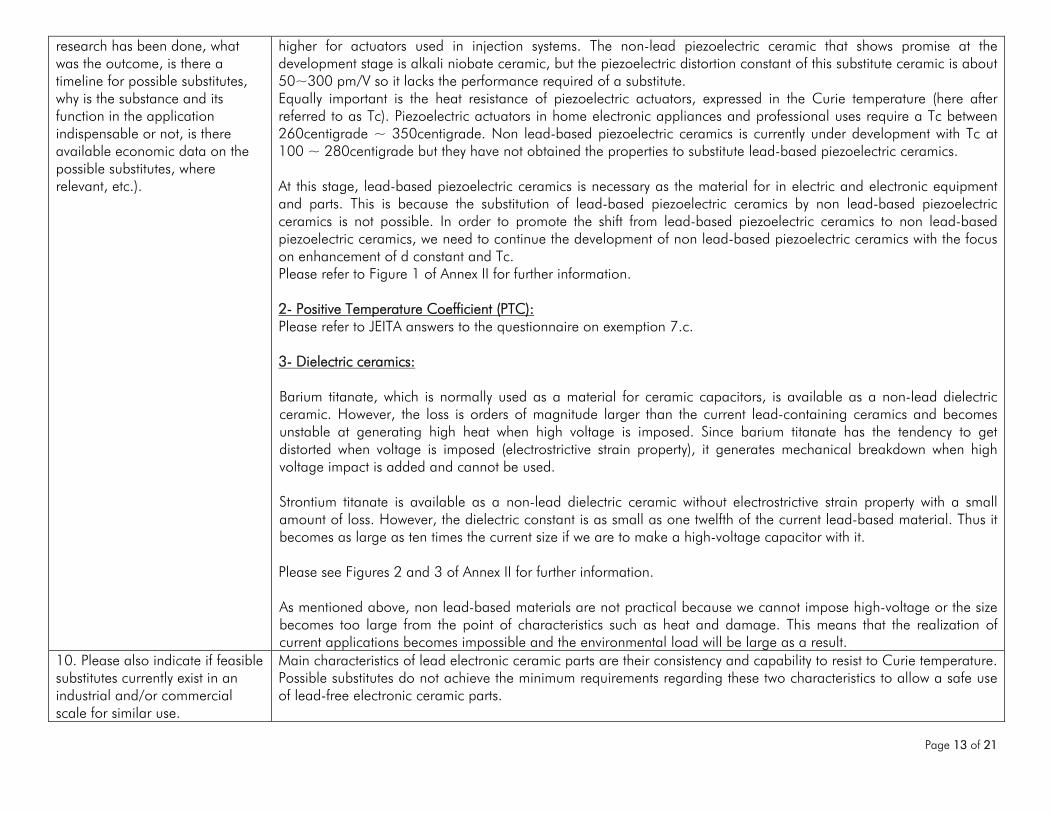
1- Piezoelectric ceramics (PZT): The piezoelectric actuators in home electronic appliances and professional uses require a piezoelectric distortion constant (d constant) of 400 pm/V or higher, similar to in-car devices. This value can go up to 700 pm/v or even
3-b-Table1: Comparison of material for high-voltage capacitors
Relativepermittivity
Dielectricloss
DC breakdownvoltage
AC breakdownvoltage
Impulsebreakdown
voltage(%) (kV/mm) (kV/mm) (kV/mm)
Current lead-basedmaterials 2700 0.04 15.3 8.0 8.0Barium titanate-basedmaterials 3000 0.80 11.8 6.7 6.0Strontium titanate 200
NotesBigger isbetter
Smaller isbetter
Bigger isbetter
Bigger isbetter
Bigger isbetter
Page 12 of 21
Page 13 of 21
research has been done, what was the outcome, is there a timeline for possible substitutes, why is the substance and its function in the application indispensable or not, is there available economic data on the possible substitutes, where relevant, etc.).
higher for actuators used in injection systems. The non-lead piezoelectric ceramic that shows promise at the development stage is alkali niobate ceramic, but the piezoelectric distortion constant of this substitute ceramic is about 50~300 pm/V so it lacks the performance required of a substitute. Equally important is the heat resistance of piezoelectric actuators, expressed in the Curie temperature (here after referred to as Tc). Piezoelectric actuators in home electronic appliances and professional uses require a Tc between 260centigrade ~ 350centigrade. Non lead-based piezoelectric ceramics is currently under development with Tc at 100 ~ 280centigrade but they have not obtained the properties to substitute lead-based piezoelectric ceramics. At this stage, lead-based piezoelectric ceramics is necessary as the material for in electric and electronic equipment and parts. This is because the substitution of lead-based piezoelectric ceramics by non lead-based piezoelectric ceramics is not possible. In order to promote the shift from lead-based piezoelectric ceramics to non lead-based piezoelectric ceramics, we need to continue the development of non lead-based piezoelectric ceramics with the focus on enhancement of d constant and Tc. Please refer to Figure 1 of Annex II for further information. 2- Positive Temperature Coefficient (PTC): Please refer to JEITA answers to the questionnaire on exemption 7.c. 3- Dielectric ceramics: Barium titanate, which is normally used as a material for ceramic capacitors, is available as a non-lead dielectric ceramic. However, the loss is orders of magnitude larger than the current lead-containing ceramics and becomes unstable at generating high heat when high voltage is imposed. Since barium titanate has the tendency to get distorted when voltage is imposed (electrostrictive strain property), it generates mechanical breakdown when high voltage impact is added and cannot be used. Strontium titanate is available as a non-lead dielectric ceramic without electrostrictive strain property with a small amount of loss. However, the dielectric constant is as small as one twelfth of the current lead-based material. Thus it becomes as large as ten times the current size if we are to make a high-voltage capacitor with it. Please see Figures 2 and 3 of Annex II for further information. As mentioned above, non lead-based materials are not practical because we cannot impose high-voltage or the size becomes too large from the point of characteristics such as heat and damage. This means that the realization of current applications becomes impossible and the environmental load will be large as a result.
10. Please also indicate if feasible substitutes currently exist in an industrial and/or commercial scale for similar use.
Main characteristics of lead electronic ceramic parts are their consistency and capability to resist to Curie temperature. Possible substitutes do not achieve the minimum requirements regarding these two characteristics to allow a safe use of lead-free electronic ceramic parts.

Page 14 of 21
Even if some substitutes fulfill the use characteristics in laboratory, it is currently extremely difficult to achieve stable results in mass production. – For example, monolithic multilayer-components with lead-free substitute materials have not even been realized on a lab scale; so there is a long way to go until industry has substitutes available at the production scale.
11. Please indicate the possibilities and/or the status for the development of substitutes and indicate if these substitutes were available by 1 July 2006 or at a later stage.
Please see question 8. Substitute materials were not available on 1 July 2006, and since considerable development work is still needed it is not possible to predict exactly when substitutes would be available on an industrial scale.
12. Please indicate if any current restrictions apply to such substitutes. If yes, please quote the exact title of the appropriate legislation/regulation.
The potential substitute materials being researched are not restricted.
13. Please indicate benefits / advantages and disadvantages of such substitutes.
Main disadvantages of lead-free ceramics: o massive temperature dependency of all properties (much higher than lead containing), o low stiffness and high Ferro elastic flexibility, o material is produced in batches, very high variance on all properties depending on batch, o moisture dependency of all raw material, o large amount of organic material needed for processing (e.g. isopropanol) which involves environmental
disadvantage comparing to lead electronic ceramic parts – such as VOC (volatile organic compound), even part of SAM reporting,
o monolithic multilayer-components not even realized on lab scale; so a long way to go until industry production scale.
Please also refer to question 8.
14. Please state whether there are overlapping issues with other relevant legislation such as e.g. the ELV Directive that should be taken into account.
A technically identical exemption exists in the ELV Directive: ELV exemption no. 11 ‘Electrical components which contain lead in glass or ceramic matrix compound except glass in bulbs and glaze of spark plugs’. ELV exemptions are currently under revision. The final recommendations from the Oko Institut regarding the revision of the exemption no. 11 are the following: ‘The stakeholders provided plausible and comprehensive information on the necessity of lead in ceramics and in thickfilm technology circuits, and on the functional necessity of these ceramics and thickfilm applications. Lead-free ceramics and in parts also thickfilm materials are available, but not on an industrial scale, or with properties that are relevantly inferior to those of the lead-containing ones for use in the applications mentioned. Based on the available information it can be concluded that the use of lead in these applications at the current state of the art is not avoidable. The stakeholders decided that the current exemption wording covers all their relevant uses of lead in ceramics. It is hence recommended to continue the exemption with the current wording.’
Page 15 of 21
Current developments in the ELV exemption request review should be taken into account, as the technical and scientific background for both the exemptions in the RoHS Directive and the ELV Directive is identical.
15. If a transition period between the publication of an amended Annex is needed or seems appropriate, please state how long this period should be for the specific application concerned.
Lead-free monolithic multilayer-components have not been realized yet at laboratory scale. Industry cannot provide any roadmap for an industry production scale for the moment. Therefore, it seems inappropriate for EICTA members to state a sunset date for the exemption 7.c, and so EICTA cannot speculate on a transition period.
16. Additional comments EICTA members may receive further technical inputs from their suppliers after EICTA deadline for internal approval. We will be happy to share these inputs with the Oko Institut after the consultation ends. Please refer to JEITA contribution to this consultation. JEITA groups the main suppliers of electronic ceramic parts worldwide, and experts on this issue. EICTA member consider their contribution high valuable, and kindly ask the Oko Institut to take into account JEITA inputs in addition to EICTA one.

Page 16 of 21
Specific questionnaire 1. What are the different applications of lead in electronic ceramic parts?
Please refer to question 2 of the general questionnaire.
2. What is the amount of lead per application, the lead content in the homogeneous material, the annual production volume as well as the number of applications related to exemption 7(c) put on the EU market annually?
Please refer to question 5 of the general questionnaire.
3. Please explain whether and how lead can be substituted in the different applications in ceramics.
- PZT ceramics: No viable alternatives. - PTC ceramics: No viable substitution of PTC ceramics at the present time. There can be candidate materials for the alternative, but such ceramics does not seem viable in the market now.
4. Please provide a roadmap or similar evidence with activities, milestones and timelines towards the replacement of lead in these applications.
No roadmap, milestones nor timelines are yet available within industry on alternatives of lead in electronic ceramic parts. As mentioned under the stakeholder consultation for the revision of the ELV Directive exemptions, substitutes for piezoelectric and dielectric ceramics have not been found. The definition of a precise roadmap needs to take into account the economical impact on electronic ceramic parts manufacturers worldwide. Therefore, it is currently very difficult to provide such a roadmap. Industry cannot provide any sunset date for the replacement of lead electronic ceramic parts for the moment. Investigations and R&D activities on possible lead-free alternatives are still going on; therefore there is still a long way to go until industry production scale. This is the reason why the timelines for lead-free piezo-electronic and dielectric ceramics – provided below – become broken lines after 2016. Please find below the roadmap for substitution provided by JEITA under the stakeholder consultation for the revision of the ELV Directive exemptions:

1- Piezoelectric ceramics In case ceramics with substitute function is supplied on a mass-production basis, it is estimated that it will take approximately 5 to 10 years to develop an application which can be employed to replace in electric and electronic equipment and parts. Thus, considering the current technology level and development progress, it is reasonable to maintain the exemption of 7.c as difficult-to-substitute technology. 2- Positive Temperature Coefficient (PTC): Please refer to JEITA answers to the questionnaire on exemption 7.c. 3- Dielectric ceramics: Capacitors with potential substitute materials will be developed, evaluated and substituted in sequence. However, due to the wide usage and the large number of units used, it may generate confusion in the market unless an appropriate transition period is provided.
5. Do you consider thickfilm applications to be covered by the current wording of exemption 7(c)?
The intermediate joint layer gets completed in the boundary of the ceramic part and the electrode part (=thickfilm) as some of the constituents of the both parts penetrate into the layer. Consequently, this intermediate joint layer gets integrated with the ceramic and the thickfilm and they cannot be separated. Thus these three layers form one homogeneous material. Therefore, the lead, which penetrated from the ceramic part into the thickfilm in joining, may be detected in this homogenous film. This lead constituent is originally from the ceramic part.
Page 17 of 21

Therefore, EICTA consider thickfilm applications to be covered by the current wording of exemption 7.c.
Page 18 of 21

Page 19 of 21
Annexes Annex I - Applications of PZT in EEE Components Application Product
Oscillator Clock
Car audio, car navigation, mobile phone, digital still camera, PC, PDS, HDD, optical disk drive, Li ion battery pack, LCD TV, PDP TV, CTV, VTR, video game, cordless phone, portable audio, home audio, printer, air conditioner, refrigerator, washing machine, microwave, smoke alarm, medical equipment
Filter AM/FM radio receiver Car audio, car navigation, mobile phone, portable audio, home audio Filter LCD TV, PDP TV, CTV, VTR, IF filter PHS, cordless phone
Buzzer Car audio Car audio, car navigation, digital still camera, PC, video game, air conditioner, refrigerator, washing machine, microwave, smoke alarm, medical equipment
Sensor Sensing of angular velocity Car audio, car navigation, digital still camera, digital video camera, interchangeable lens, video game
Sensing of acceleration Digital video camera, HDD, optical disk drive, watch Sensing of infrared ray Security gadgets and gizmos, lightning system Sensing of ultrasonic Fuel cell, scanner, medical equipment, fish finder Phonating Phonating of ultrasonic Fuel cell, scanner, medical equipment, fish finder Actuator Actuating of auto focus lens Mobile phone, digital still camera Actuating of optical zoom lens Mobile phone, digital still camera Actuating of ultrasonic motor Digital still camera, roll screen Actuating of magnetic head HDD Actuating of print head Color printer, large format printer, impact dot matrix printer Stabilizer Image stabilizer Mobile phone, digital still camera, digital video camera Transformer AC adaptor PC Inverter Display backlighting inverter PC
Pump Cooling System with piezoelectric pump
PC

Annex II – Data / evidence on why substitution is impracticable
1- Piezoelectronic ceramics Figure 1: Technological map of piezoelectric ceramics from aspect of Tc and d33
Tcとd33から見るPbフリー圧電セ ラミックスの技術マップ
0
100
200
300
400
500
600
700
800
0 50 100 150 200 250 300 350 400
キュリー温度Tc(℃)
圧電歪定数d33(pm/V)
発振子,狭帯域フィル タ
振動子,広帯域フィル タ
ア クチ ュエ ー タ,音響,セ ンサ
●:鉛系圧電材料●:非鉛系圧電材料
: Lead-based piezoelectric material : Non lead-based piezoelectric material
Actuators, Acoustic,
Curie temperature Tc (�)
Piezoelectric distortion constant d33 (pm/V)
Oscillators, broad-band filters
Oscillators, narrow-band filters
Technological map of Pb-free piezoelectric ceramics from the aspect of Tc and d33
Page 20 of 21

Page 21 of 21
3-b-Table1: Comparison of material for high-voltage capacitors
Relativepermittivity
Dielectricloss
DC breakdownvoltage
AC breakdownvoltage
Impulsebreakdown
voltage(%) (kV/mm) (kV/mm) (kV/mm)
Current lead-basedmaterials 2700 0.04 15.3 8.0 8.0Barium titanate-basedmaterials 3000 0.80 11.8 6.7 6.0Strontium titanate 200
NotesBigger isbetter
Smaller isbetter
Bigger isbetter
Bigger isbetter
Bigger isbetter
2- Dielectric ceramics
Figure 2: Structure of a high-voltage capacitor
Figure 3: Comparison of material for high-voltage capacitors
Insulating paint Electrically conductive wire
Solder
Electrode
Ceramic base material