Embed Size (px)
Citation preview
Jitter Analysis with the R&S®RTO Digital Oscilloscope Application Note
Products:
ı R&S®RTO1002
ı R&S®RTO1004
ı R&S®RTO1012
ı R&S®RTO1014
ı R&S®RTO1022
ı R&S®RTO1024
ı R&S®RTO1044
ı R&S®RTO-K12
This application note introduces the Jitter analysis
capabilities of the R&S®RTO Digital Oscilloscope
and the Jitter option R&S®RTO-K12 for digital
signals.
It provides background information on jitter sources
and standard jitter measurement tools. Furthermore
it demonstrates Period jitter, Cycle jitter and Time
Interval Error jitter measurements based on an
application example. The benefits of different
representations of the measurement results with
histogram, track and spectrum display are
discussed.
Dr.
Math
ias H
ellw
ig
8.2
013 -
1T
D03_2e
Applic
ation N
ote

Table of Contents
1TD03_2e Rohde & Schwarz - Jitter Analysis with the R&S®RTO Digital Oscilloscope 2
Table of Contents
1 Introduction .................................................................................................... 3
2 Background on Jitter ................................................................................... 5
2.1 Jitter Definition .................................................................................................... 5
2.2 Jitter Sources ...................................................................................................... 5
2.2.1 Random Jitter........................................................................................................ 6
2.2.2 Periodic Jitter ........................................................................................................ 6
2.2.3 Data-Dependent Jitter............................................................................................ 6
2.2.4 Duty-Cycle Distortion ............................................................................................. 8
2.3 Jitter Analysis Tools ............................................................................................ 9
2.3.1 Statistics ............................................................................................................... 9
2.3.2 Persistence ......................................................................................................... 10
2.3.3 Histogram ........................................................................................................... 11
2.3.4 Track .................................................................................................................. 13
2.3.5 Spectrum ............................................................................................................ 13
2.3.6 Eye Diagram ....................................................................................................... 13
2.4 Instrument Limitations for Ji tter Analysis ......................................................... 15
3 Jitter Measurements .................................................................................. 17
3.1 Period Jitter ....................................................................................................... 18
3.2 Cycle-Cycle Jitter .............................................................................................. 18
3.3 Time Interval Error Jitter.................................................................................... 18
3.4 Unit Interval and Data Rate ................................................................................ 19
3.5 Eye opening / Mask test..................................................................................... 20
4 Application Example .................................................................................. 21
4.1 Measurement Setup with the Jitter Wizard ........................................................ 21
4.2 Period Jitter Measurement ................................................................................ 23
4.3 N-cycle Jitter Measurement ............................................................................... 27
4.4 TIE Jitter Measurement...................................................................................... 30
5 Conclusion.................................................................................................... 34
6 Literature ....................................................................................................... 35
7 Ordering Information ................................................................................. 36
Introduction
1TD03_2e Rohde & Schwarz - Jitter Analysis with the R&S®RTO Digital Oscilloscope 3
1 Introduction
This application note presents the capabilities of the R&S®RTO-K12 Jitter Analysis
option for the R&S®RTO Digital Oscilloscope with respect to the jitter analysis of data
and clock signals. In the following, the term R&S®RTO Digital Oscilloscope will be
abbreviated as RTO and the R&S®RTO-K12 Jitter analysis option as RTO-K12 for
simplified reading.
Digital interfaces have become predominant in electronic design with the rise of the
digital computer and the associated digital signal processing and digital transmission.
Though digital signals are more robust and less susceptible to disturbances than
analog signals, the trend to increase the data rate and clock speed reduces the timing
margin for these signals. It also requires more detailed analysis and a highly
sophisticated test and debug capabilities, if failures occur. As an example of the
increase of clock speed over several generations, some well-known digital interface
standard families are listed, like PCIe, SATA, USB or DDR.
The analysis of the timing margin is not limited to the data signal itself, it is also
applicable to the embedded clock, or the reference clock. Moreover some of the jitter
measurements are applicable to different, non-digital areas, like modulated RF signals
or timing characterization of analog-to-digital converter (ADC) and digital-to-analog
converter (DAC).
In combination with the RTO-K12 option, the RTO is an excellent platform for precise
jitter analysis. The RTO’s key features for precise signal integrity measurements are a
sensitive, wideband, low noise analog front-end, a high precision, single core ADC and
a high acquisition and processing rate. The RTO-K12 adds automated measurements
for jitter characterization, software based clock data recovery, a track graph of
measurements and a wizard tool to ease the use of the jitter analysis option. The
RTO®RTO-K13 Clock Data Recovery (CDR) option provides additional capabilities for
jitter analysis, which is not further discussed in this application note. It enables a
configurable hardware-based CDR for triggering on data signals that contain an
embedded clock.
Jitter measurements are possible in the time domain or the frequency domain.
Oscilloscopes natively measure signals in the time domain. An example of a dedicated
instrument for jitter measurements in frequency domain is the R&S®FSUP Signal
Source Analyzer for Phase Noise and VCO test (1). The comparison in Table 1-1
shows that the accuracy is higher for measurements with frequency domain based
instruments due to a typically higher dynamic range, longer measurement interval and
a dedicated measurement concept for phase noise. Jitter measurements with Phase
Noise and Spectrum Analyzers, however, are limited to clock signals only. Jitter
Measurements in the time domain allow analysis of digital binary data or to track the
phase noise signal over time.
In the first chapter the application note provides some background on jitter, focusing on
jitter sources, analysis methods and instrument limitations for jitter analysis. Next, it
introduces a signal model, which is used to explain the jitter measurements and the
impact on analysis methods. In the last chapter, this application note uses an RTO with
the RTO-K12 to analyze a digital clock signal of the Rohde & Schwarz Demo board.

Introduction
1TD03_2e Rohde & Schwarz - Jitter Analysis with the R&S®RTO Digital Oscilloscope 4
Three widely used jitter measurements are applied to the clock signal, and showcase
the Jitter analysis capabilities of the RTO.
Differences of Differences of Time vs. Frequency Domain based Instrument
Time Domain Frequency Domain
Intrinsic
measurements
Peak-Peak Jitter
Cycle-Cycle Jitter
Period Jitter
RMS Phase Jitter
Phase Noise
Jitter Frequency information
Benefits
Good w ith low frequency clocks
Good w ith Data-Dependent Jitter
Monitor jitter over time
Easy detection of spurs vs. Random Jitter
Low Noise Floor
Table 1-1: Differences of Time vs. Frequency Domain based Instruments
A detailed analysis of the impact of a clock data recovery algorithm that is part of the
Time Interval Measurement (TIE) is not within the scope of this application note, and
the reader may follow the references to obtain more information on this topic.

Background on Jitter
1TD03_2e Rohde & Schwarz - Jitter Analysis with the R&S®RTO Digital Oscilloscope 5
2 Background on Jitter
2.1 Jitter Definition
The International Telecommunication Union (ITU) provides a widely accepted definition
of timing jitter (2): "Jitter is the short-term variations of the significant instants of
deviation of timing signal from their ideal positions in time (where short -term implies
that these variations are of frequency greater than or equal to 10 Hz)." It is measured
with reference to an ideal clock source or to itself.
Due to random jitter components, statistical values like standard deviation or peak-to-
peak are used to quantify jitter. Like all statistical measurements, the user should
specify a qualitative statement, for example a confidence interval, to ensure repeatable
measurements.
The ITU further distinguishes between jitter and wander. In that context, Jitter has
frequency components only above 10 Hz, while wander is only below. A further
consideration into wander is outside the scope of this application note.
2.2 Jitter Sources
Jitter typically consists of various components that are caused by different jitter
sources, see Figure 2-1. For the analysis of jitter it is important to understand these
sources and the contributions to the total jitter (TJ). For an analytical approach, a jitter
model is frequently used, which splits jitter into the two major categories of Random
and Deterministic Jitter.
Data-Dependant Jitter (DDJ)Duty-Cycle Distortion (DCD) Periodic Jitter (PJ)
Deterministic Jitter (DJ)(bounded)
Random Jitter (RJ)(unbounded)
Total Jitter (TJ)
Figure 2-1 Jitter Sources
Deterministic Jitter (DJ), also called systematic jitter, is further broken down into
Periodic Jitter (PJ), Data-Dependent Jitter (DDJ) and Duty-Cycle Distortion (DCD).
Deterministic jitter is bounded and specified as peak-to-peak value. Random Jitter is
unbounded and commonly specified by the standard deviation σ.

Background on Jitter
1TD03_2e Rohde & Schwarz - Jitter Analysis with the R&S®RTO Digital Oscilloscope 6
It is important for the user to understand and differentiate the jitter sources and the
associated probability density function (PDF), because the histogram is a powerful tool
for the jitter analysis. However, the interpretation of the histogram can be difficult and
requires a good understanding of the underlying effects. The next sections discuss the
PDF for all individual jitter sources, because the total jitter is calculated by a
convolution of the individual PDFs of each jitter source (3).
2.2.1 Random Jitter
Due to its irregular nature, Random jitter (RJ) is uncorrelated to any other signal and
unpredictable in timing behavior. It is described in the time domain and has its
equivalent with phase noise in the frequency domain (4). Thermal noise, shot noise, 1/f
noise and other physical effects are contributions to random jitter, and a random
process is its mathematically representation. The PDF of the random jitter is the well-
known Gaussian distribution, see equation (2-1) and Figure 2-2, where the mean value
μ is the nominal oscillator period and σ is the standard deviation. With the given PDF,
the random jitter turns out to be unbounded, and is usually specified by the standard
deviation σ. Sometimes a peak-to-peak measurement over a defined sampling interval
is used to describe the random jitter.
( )
√ ( )
(2-1)
The reason for explicitly referring to the normal distribution of the random jitter is
twofold. First, the thermal noise contribution to the random jitter shows already a
normal distribution. Secondly, due to the central limit theorem, other contributing
physical effects with well-defined distributions converge into the observed normal
distribution.
2.2.2 Periodic Jitter
Periodic Jitter (PJ) is caused by a periodic disturbance. Though this signal is not
necessarily sinusoidal, it is frequently also named sinusoidal jitter. The amplitude of the
periodic signal bounds the jitter. A sinusoidal disturbanc e signal has a PDF given in
equation (2-2) and shown in Figure 2-3.
( ) { √( ) | |
| | (2-2)
A strong local RF oscillator, a switch-mode power supply, undesired crosstalk or an
unstable, oscillating PLL cause period jitter due to an unintentional coupling into the
signal.
2.2.3 Data-Dependent Jitter
Inter Symbol Interference (ISI) causes Data-Dependent Jitter (DDJ). When ISI is
present, the signal is disturbed with an attenuated, time-shifted copy of itself or spectral
parts of itself.

Background on Jitter
1TD03_2e Rohde & Schwarz - Jitter Analysis with the R&S®RTO Digital Oscilloscope 7
Figure 2-2 Normal Distribution ( )
Figure 2-3 Sinusoidal PJ Distribution (A=.5)

Background on Jitter
1TD03_2e Rohde & Schwarz - Jitter Analysis with the R&S®RTO Digital Oscilloscope 8
In the time domain, ISI is caused by multipath propagation for wireless and reflections
for wired transmission that create time-shifted copies of the signal. Reflections, or
echoes, occur because of impedance mismatch of the termination as well as physical
media discontinuities in the transmission path, like connectors or edges.
In the frequency domain, dispersion creates ISI. Dispersion is a frequency dependent
group velocity of the transmission media, introduced by material or modal effects of
transmission paths. Bandwidth limitations of the transmission media clearly show
frequency dependent group velocity, but ISI in the frequency domain is not restricted to
bandwidth limitations.
The most common model of the PDF for DDJ shows two distinct amplitudes, which
results in a dual Dirac PDF, see Figure 2-4 and equation (2-3).
( )
( ( ) ( )) (2-3)
Figure 2-4 Dual-Dirac DDJ Distribution ( )
2.2.4 Duty-Cycle Distortion
Duty-Cycle Distortion (DCD) is the result of two effects. The first effect is caused by the
decision level marked with a letter A in Figure 2-5. If the decision level of a signal is
altered and not coincident with the optimal decision level, the resulting mismatch
introduces DCD. Figure 2-5 shows a raised decision level, which always retards the
rising edge at Δtar and advances the falling edge at Δtaf . Usually the standard of a data
interface defines the decision level for the specific signal, whereas the crossing of
rising and falling edges in the eye diagram determines the optimal decision level.

Background on Jitter
1TD03_2e Rohde & Schwarz - Jitter Analysis with the R&S®RTO Digital Oscilloscope 9
Similar to the DDJ, the PDF of this jitter histogram becomes a dual Dirac PDF (see
Figure 2-4).
Different rise and fall times of a signal cause the second effect, marked with a letter B
in Figure 2-5. The duty-cycle error of a high to low transition Δtbr of a binary signal will
differ from a low to high transition Δtbf proportional to the difference between rise and
fall time.
Overall the DCD is bounded like all deterministic jitter sources, though it is difficult to
differentiate between DCD and DDJ introduced by ISI. A way to measure these
contributions separately is the jitter measurement of a binary, alternating '01'
sequence, essentially a binary clock signal. It will eliminate the ISI due to the periodic
nature.
Δtar Δtaf Δtbr Δtbf
A B
Decision
Level
Clock
Data
Altered
Decision
Level
Figure 2-5 Duty-Cycle Distortion (DCD)
2.3 Jitter Analysis Tools
The RTO offers several analysis functions to evaluate signal integrity. The jitter
analysis option RTO-K12 extends this set of functions to analyze several types of
signals, like digital clock and binary data signals, as well as RF signals,.
As a distinction, digital clock signals are specified in units of Hertz [Hz] as opposed to
binary data signals, which are specified in units of bits per seconds [bps]. A digital
clock signal can be regarded as a binary data signal of a perpetual sequence of '01's,
just that the data rate is double the frequency. The user can analyze clock signals by
applying the same measurement and visualization functions as for binary data. Using
this analogy, all measurement and analysis tools apply to clock signals. Conversely
measurements like frequency, period, cycle-cycle, or N-cycle jitter apply only to
periodic digital clock and RF signals.
2.3.1 Statistics
The automatic measurement function of the RTO provides statistical data for any
automated measurement. Typical jitter measurements that require statistical evaluation
are frequency, period or pulse width measurements. As the measured data contain
random components by nature, statistic values are appropriate to describe the signal

Background on Jitter
1TD03_2e Rohde & Schwarz - Jitter Analysis with the R&S®RTO Digital Oscilloscope 10
properties. Well known are mean value and standard deviation as mathematical
expressions of the PDF (5).
As previously explained, the user should use the standard deviation if random jitter
components are present. In case of Deterministic Jitter, the user can calculate the
peak-to-peak jitter by subtracting the '+Peak' from the '-Peak' of the RTO
measurement.
The number of measurements is an important point to evaluate the confidence in the
measurement results. The high acquisition rate of the RTO is an advantage to gain
high measurement confidence in short time. For data with known PDF, the user can
verify the confidence of the statistics (5).
Statistics can be enabled in the RTO’s "Meas" menu > "Setup" tab. By default the RTO
takes only one measurement per waveform. The user can configure the RTO to take
multiple measurements, by defining the number of measurements within one
acquisition in the "Meas" menu > "Gate/Display" tab, Figure 2-6.
Figure 2-6 Selection of multiple measurements (“Multiple meas”) per waveform
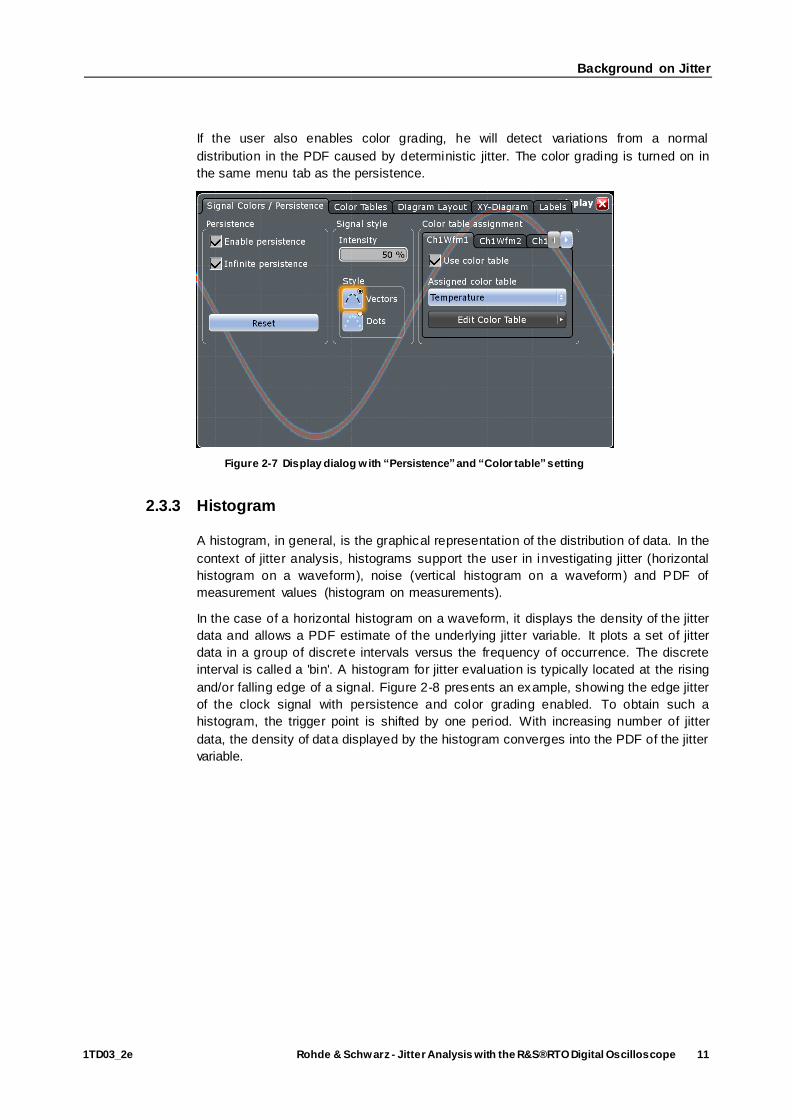
2.3.2 Persistence
A simple way to measure jitter is the use of the display persistence, which emulates
the phosphorous screen of an analog oscilloscope ("Display" > "Signal Colors /
Persistence"), Figure 2-7 . Once the persistence is set to infinity, the RTO will
accumulate the waveforms on the display and the user can, for example, apply cursors
to measure the spread of the crossing points of an eye pattern in order to determine
the total jitter for a given time or sample size. Figure 2-7 shows an example for
persistence and color grading, including a measurement of the total jitter with cursors.
Background on Jitter
1TD03_2e Rohde & Schwarz - Jitter Analysis with the R&S®RTO Digital Oscilloscope 11
If the user also enables color grading, he will detect variations from a normal
distribution in the PDF caused by deterministic jitter. The color grading is turned on in
the same menu tab as the persistence.
Figure 2-7 Display dialog with “Persistence” and “Color table” setting
2.3.3 Histogram
A histogram, in general, is the graphical representation of the distribution of data. In the
context of jitter analysis, histograms support the user in investigating jitter (horizontal
histogram on a waveform), noise (vertical histogram on a waveform) and PDF of
measurement values (histogram on measurements).
In the case of a horizontal histogram on a waveform, it displays the density of the jitter
data and allows a PDF estimate of the underlying jitter variable. It plots a set of jitter
data in a group of discrete intervals versus the frequency of occurrence. The discrete
interval is called a 'bin'. A histogram for jitter evaluation is typically located at the rising
and/or falling edge of a signal. Figure 2-8 presents an example, showing the edge jitter
of the clock signal with persistence and color grading enabled. To obtain such a
histogram, the trigger point is shifted by one period. With increasing number of jitter
data, the density of data displayed by the histogram converges into the PDF of the jitter
variable.

Background on Jitter
1TD03_2e Rohde & Schwarz - Jitter Analysis with the R&S®RTO Digital Oscilloscope 12
Figure 2-8 Histogram of the rising edge of a clock signal
With the RTO it is also possible to display the histogram of a measurement function for
a detailed analysis of the PDF. The user enables it in
"Meas" menu > "Long Term/Track" tab, Figure 2-9. Within this tab, the user has the
option to scale the histogram manually, by entering the offset and scale, or let the RTO
do this by checking the "Continuous auto scale" box.
Figure 2-9 Selection of Histogram or Track display for measurement results

Background on Jitter
1TD03_2e Rohde & Schwarz - Jitter Analysis with the R&S®RTO Digital Oscilloscope 13
2.3.4 Track
The track curve of a jitter measurement displays the measurement results over time for
an acquired waveform. Unlike the histogram, it reveals trends of change in the analysis
and preserves the timing relationship of the measurement results to the signal. This is,
for example, useful for frequency modulated signals, as the track curve of the period
measurement of the waveform can reveal the modulating signal. Similarly, the period
track might also show unintentional disturbances, due to coupling and cross talk, which
are, in the same way, modulating signals. Like the histogram, track is enabled in
"Meas" menu > "Long Term/Track". The vertical scaling can be set in the same way as
for the histogram.
As a side note, the RTO offers a Long Term function in the same menu. There is a
difference between the track and the long term function. The track shows multiple
measurements per acquisition and every acquisition displays a new track curve, while
the Long Term curve takes one measurement per acquisition and displays it over
multiple acquisitions.
2.3.5 Spectrum
The spectrum displays the acquired signal in the frequency domain. The RTO creates
the spectrum of the signal waveform by calculating the FFT. The sampling rate
determines the maximal frequency of the spectrum, and the ratio between the
sampling rate and the number of samples defines the resolution of the spectrum.
Additionally, the introduced track function allows a Fast-Fourier-Transform (FFT) of the
track curve due to its timing information. This is a significant benefit of real-time
oscilloscope like the RTO over sampling oscilloscopes. Traditionally sampling
oscilloscopes have been used for jitter analysis, but their analysis capabilities are
limited to histogram data.
If there is no strong modulation on the signal, the jitter track looks like a noise signal.
The benefits of the spectrum of a track signal are twofold. First, small signals, which
are obscured by the noise in the time domain, become visible in the spectrum.
Secondly, the spectrum of the track signal shows the noise floor, which is an
equivalent to the signal power, and the spectral shape of the jitter signal gives
indications about noise contributions (see chapter 2.2.1).
2.3.6 Eye Diagram
An eye diagram helps to determine the signal quality of digital data signals. Overlaying
multiple waveforms of a digital signal creates an eye diagram, Figure 2-10. Usually the
eye diagram is displayed over a horizontal range of 1.5 to 2 unit intervals (UI) or bit
periods of the digital signal. The user should pay attention to following hints for the
creation of an eye diagram of a digital signal:
The timing of the overlay must be related to a reference clock, that can be either an
embedded clock signal or an external clock signal. The embedded clock signal must
be extracted by hardware or software CDR.

Background on Jitter
1TD03_2e Rohde & Schwarz - Jitter Analysis with the R&S®RTO Digital Oscilloscope 14
For accurate measurements, all relevant bit pattern of the digital signal should be
included in the eye diagram. Memory effects like ISI (see chapter 2.2.3) determine the
number of relevant bits for the pattern, it specifies how much one bit of the digital
signal influences its neighbors. For example, a standard edge trigger would exclude
patterns, which follow just a falling edge. For better results, the trigger should be set at
least to both rising and falling edge. The preferred way to generate an eye diagram is
based on a clock data recovery (CDR). If a digital signal has an embedded clock, a
CDR recovers this clock out of the signal and the oscilloscope may use it for trigger
and display. The RTO offers an integrated HW CDR solution (R&S®RTO-K13) to
generate an eye diagram.
1 0 1 0 0 1 1 1 0 1
Oscilloscope
Display0
1
2
3
4
5
6
7
8
9
Figure 2-10 Generation of an Eye pattern

Background on Jitter
1TD03_2e Rohde & Schwarz - Jitter Analysis with the R&S®RTO Digital Oscilloscope 15
2.4 Instrument Limitations for Jitter Analysis
In order to get meaningful results out of a jitter analysis, the user should pay attention
to certain aspects of the measurement.
The first and most obvious aspect is the bandwidth of the digital oscilloscope. Based
on the frequency of a digital clock signal or the bit period of a digital data signal, the
Nyquist criterion must be met. This is necessary but not sufficient. Digital signals can
have a low data rate or clock frequency, but still a fast rise or fall time implying high
spectral components in the signal. The user can calculate the required bandwidth
according to the following rule of thumb ( ) . The analog input
bandwidth of the oscilloscope shall be bigger than the signal bandwidth. If probes are
used, the user must also take the impact of their bandwidth into account, which
changes the system bandwidth approximately to a value given in equation (2-4). The
sampling rate should be at least twice the signal bandwidth to fulfill the Nyquist
criterion. Further resolution can be achieved by interpolation techniques like ⁄
interpolation.
√
(2-4)
Another important aspect is the impact of the signal level and transition time (rise or
fall). If the signal level is small or the transition time is high, the input noise of the
analog front end of the oscilloscope VN might become a dominant part in the jitter
analysis, see Figure 2-11. The influence of the transition time for the sampling
accuracy Δt is shown with a fast transition Δts and a slow transition Δtl. A larger
amplitude VA will reduce the transition time. Generally the ratio of vertical scale to the
associated RMS noise voltage improves towards larger vertical scales. The
interpolation, which is used to determine the signal crossing with the threshold and
consequently the accuracy, will greatly benefit from this and an optimal vertical scaling.
time
VA
VN
Δts Δtl
Figure 2-11 Influence of noise on time measurement accuracy
Another aspect is the stability of the time base, long term as well as short term. The
variations of the oscilloscope’s internal time reference add noise to the acquired signal.
The integrated oscillator used as the reference clock causes long term variations. The
voltage controlled oscillator (VCO) of the PLL multiplies the reference clock to the
sampling frequency, which creates short term variations.
Finally, the noise influence and the time base stability define an int rinsic limit for jitter
measurements of an oscilloscope. This limit is the jitter noise floor (JNF), which

Background on Jitter
1TD03_2e Rohde & Schwarz - Jitter Analysis with the R&S®RTO Digital Oscilloscope 16
describes the outermost limit to which the jitter of a signal can be measured under
optimal conditions. Equation (2-5) defines the JNF ( ), which is frequently named as
the time RMS value.
▪ : input referred noise [VRMS]
▪ : signal amplitude [V]
▪ : full scale range
▪ : rise time 10-90% [s]
▪ : aperture uncertainty [sRMS]
√ (
)
(2-5)
Without providing the exact derivation of equation (2-5), a brief rational shall be
presented. As described the JNF is caused by noise and slew rate in the threshold
point and the short term variation of the sampling clock (see Figure 2-11). The first
term represents the noise / slew rate effect, the second term the short term variation of
the sampling clock. Both together are random, independent variables, so that the total
JNF can be calculated as the square root of the sum of the squares.
The jitter noise floor for digital real -time oscilloscopes is typically in the region of 1 to
5 ps RMS. It equals the standard deviation of the period jitter, cycle-cycle, or time-
interval measurement (TIE). Preferred is the TIE measurement, because it neglects the
long term stability of the reference clock due to the ideal estimated clock (explained in
chapter 3.3).
Finally it should be mentioned that oscilloscopes typically have a delta time accuracy
(DTA) specification, which is a measure for jitter accuracy. It corresponds to the time
error between two edges of the same acquisition and channel. This parameter closely
relates to the JNF and usually specified as peak-to-peak value, with an additional term
for the long term variation.

Jitter Measurements
1TD03_2e Rohde & Schwarz - Jitter Analysis with the R&S®RTO Digital Oscilloscope 17
3 Jitter Measurements
The RTO with the RTO-K12 option supports a wide range of automated jitter
measurements that are selected in the measurement dialog, Figure 3-1.
Figure 3-1 RTO measurement dialog with the selection of jitter measurements
This section provides the definition of the most important jitter measurements which
are Period / Frequency jitter, Cycle-cycle jitter, Time Interval Error (TIE) and Unit
Interval (UI) / Data Rate. Figure 3-2 gives a graphical representation of these jitter
measurements with the example of a clock signal.
TIE1 TIE2 TIE3 TIE4
P1P2
P3
Ideal Edge
Positions
Acquired
Waveform
C2=P2-P1 C3=P3-P2
Tref1 Tref2 Tref3 Tref4
Figure 3-2 Jitter definition of period (P1), cycle-cycle (C2) and TIE jitter

Jitter Measurements
1TD03_2e Rohde & Schwarz - Jitter Analysis with the R&S®RTO Digital Oscilloscope 18
3.1 Period Jitter
Period and Frequency jitter can be used interchangeably as they are reciprocal to each
other. An oscilloscope is an instrument measuring in the time domain, so the period
jitter analysis is preferred over the frequency jitter analysis , because it avoids precision
errors in the reciprocal.
Period jitter allows the user to evaluate clock stability. With the help of the track display
a modulation signal can be visualized, regardless whether it is intentional or
unintentional. It is not applicable for data signals. Period jitter is used to calculate
timing margins in digital systems, which rely on a fixed period to meet setup and hold
times of the internal flip-flops.
The oscilloscope calculates the period every cycle by the difference of successive
edge positions , described in equation (3-1) and shown in Figure 3-2. The period
jitter is the deviation of period to the average period, equation (3-2).
(3-1)
( ) (3-2)
3.2 Cycle-Cycle Jitter
The cycle-cycle jitter is very similar to the period jitter. It is also only applicable to
periodic signals, and there is a generalization from 1st
to the Nth
difference. Cycle-cycle
jitter lets the user evaluate the source stability and the t racking capability of a phase
locked loop (PLL).
The oscilloscope determines the cycle-cycle jitter by subtracting the period from the
subsequent period, shown in equation (3-3) and in Figure 3-2
( ) ( ) ( ) (3-3)
This expression can be generalized to an N-cycle jitter with the definition
given in equation (3-4).
( ) ( ) (3-4)
3.3 Time Interval Error Jitter
For oscilloscopes, the TIE calculates the difference of actual edge position from the
associated nth
ideal edge position (see equation (3-5) and Figure 3-2). Precisely,
this is the time error not the time interval error as defined by the ITU (2), but a
commonly used term for the analysis function in oscilloscopes. For convenience, the
term TIE will be used as time error in the remaining part of this application note instead
of time interval error.
( ) ( ) (3-5)

Jitter Measurements
1TD03_2e Rohde & Schwarz - Jitter Analysis with the R&S®RTO Digital Oscilloscope 19
The TIE is commonly used in communication systems to evaluate the transmission of a
digital data stream with an embedded clock. In particular it shows the accumulation of
jitter sources. It can be applied to digital clock signals, but preferably it is applied to
binary data signals.
For binary data signals, it might be the case that there is no transition for an ideal edge
position . In this case the oscilloscope assumes the previous value for the TIE
jitter ( ). With respect to TIE calculation equation (3-5), the oscilloscope must
determine the ideal edge position . Oscilloscopes have typically two methods to
do this.
The first and simplest approach is called the constant frequency approach. Thereby
the oscilloscope estimates the value for the interval of all using a least square
estimation (LSE) (5), so that the ideal edge position equals the nth
multiple
of the estimate and the corresponding TIE jitter is given in equation (3-6).
( ) ( )
(3-6)
The second method uses a phase lock loop (PLL) or CDR to calculate the TIE jitter.
This is necessary, because the assumption of the first method, that the frequency of
the embedded clock is constant, may not hold true for all signals. The embedded clock
may change over time intentionally due to a spread spectrum technique, or
unintentionally due to temperature drift or other effects. Spread spectrum techniques
are deployed for example in PCIe, and other standard interfaces to reduce
electromagnetic interference (EMI).
Oscilloscopes typically implement a CDR in software. The CDR calculates the ideal
edge position for a single acquisition based on the series of previous edge
positions [ ]. Each acquisition requires a new independent calculation of the
CDR. Moreover, a CDR shows a memory effect and requires a certain number of
transitions preceding the actual edge position to compute a valid ideal edge position
. This number depends on the configuration parameters, like CDR bandwidth or
order of the CDR. The result is that an oscilloscope with a software CDR cannot
calculate a valid TIE jitter ( ) for the initial edge positions and as a consequence,
the record must be reasonable large for a detailed TIE jitter analysis.
The RTO supports the constant frequency as well as the software CDR method.
Additionally the RTO has a built-in hardware CDR, which is unique for this class of
oscilloscopes. The hardware CDR runs constantly, even if the oscilloscope does not
acquire a waveform, so that, unlike the software CDR, the CDR is able to calculate a
valid, ideal edge position at the beginning of the acquisition. The hardware CDR
is enabled by the R&S®RTO-K13 option.
3.4 Unit Interval and Data Rate
For clock signals, the RTO displays the unit interval (UI) as a time difference of
adjacent rising or falling measured transitions, as stated in equation (3-1). If the signal
is a binary data signal and transitions are not equidistant in time, the measurement
function uses the embedded clock signal, recovered by the CDR to calculate the UI.

Jitter Measurements
1TD03_2e Rohde & Schwarz - Jitter Analysis with the R&S®RTO Digital Oscilloscope 20
The data rate of the signal is the reciprocal of the UI. If the user selects the data rate
measurement function, the RTO determines first the UI and then calculates the data
rate. As the initial measurement takes place in the time domain and the UI and data
rate measurement are mathematically interchangeable the UI measurement function is
preferred over the frequency measurement function.
3.5 Eye opening / Mask test
In addition to the jitter measurements discussed so far, the RTO offers also several
eye measurements and a specific mask test function, which allow mask tests with eye
diagrams. This is helpful for jitter analysis of binary data signals. In the top graph
Figure 3-3 displays the color graded eye pattern with the mask test. Mask violations
are displayed in the graph in black and recorded in the mask test dialog box of the
mask test. At the bottom of the display the eye measurement results are shown. As
these are already statistic data, the fields for statistics are left empty.
In order to make use of this feature the use of the hardware CDR is imperative. The
explanation is outside the scope of this application note.
Figure 3-3 Eye measurement and Mask Test for a TTL signal

Application Example
1TD03_2e Rohde & Schwarz - Jitter Analysis with the R&S®RTO Digital Oscilloscope 21
4 Application Example
This chapter gives a step-by-step example of a typical jitter analysis using the RTO-
K12 option. The signal source is provided by the digital clock output of the Rohde &
Schwarz Demo board. The TTL clock signal with a nominal frequency of 10 MHz is
connected with an active, single-ended 3 GHz probe R&S®RT-ZS30 (Figure 4-1). This
digital clock signal allows to focus on the jitter measurements. This digital clock signal
is a real world example and shows disturbances, caused by the design of the board.
Figure 4-1 TTL clock of the RTO demo board
4.1 Measurement Setup with the Jitter Wizard
For convenience and demonstration purpose the Jitter Wizard of the RTO-K12 option
is used to setup the measurements. It is started in the menu "Meas" > "Wizard" >
"Jitter Wizard" and brings up the start menu as shown in Figure 4-2. The "period and
frequency" measurement is preselected, and the "Next" button gets the user to the
"configuration" tab, see Figure 4-3. Channel 1 is preselected, and again pressing the
"Next" button brings the user to the "autoset" tab, see Figure 4-4. In order to retain the
favorable, vertical settings, the "Retain current settings" in the vertical scaling section is
selected. Another "Next" button gets the user to the final "results plot" tab (Figure 4-5).
All four analysis options are selected and a click on the "Execute" button will display
the period jitter analysis.
The individual measurement results will be presented in the following sub-chapters.

Application Example
1TD03_2e Rohde & Schwarz - Jitter Analysis with the R&S®RTO Digital Oscilloscope 22
Figure 4-2 Jitter Wizard of the RTO-K12 option - Measurement selection
Figure 4-3 Jitter Wizard - Channel Selection

Application Example
1TD03_2e Rohde & Schwarz - Jitter Analysis with the R&S®RTO Digital Oscilloscope 23
Figure 4-4 Jitter Wizard - Autoset Selection
Figure 4-5 Jitter Wizard - Result plot selection
4.2 Period Jitter Measurement
The period jitter measurement was introduced in chapter 3.1. Figure 4-6 shows the
result of the Jitter Wizard execution from the previous chapter 4.1. In the top diagram
an overlay of the TTL clock waveform (blue) and period jitter t rack waveform (green)
can be seen. This is useful, because the user can immediately associate specific
deviations of the nominal period related to the waveform. The diagram in the middle
shows the spectrum of the period jitter. The lower diagram displays the period jitter
histogram ( ) , which is the PDF of the period jitter and shows a tri-modal

Application Example
1TD03_2e Rohde & Schwarz - Jitter Analysis with the R&S®RTO Digital Oscilloscope 24
Gaussian distribution. The table at the bottom of the screen shot displays the
measurement results for the period and frequency including the statistical data.
Figure 4-6 Jitter Wizard result for the TTL clock
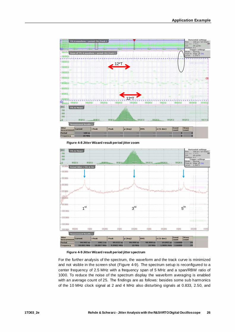
In a next step, the record length is increased to 4 Msamples, to analyze the PDF in
more detail and to get better resolution in the spectrum. Figure 4-7 shows the result of
the increase in record length. As a side effect, the number of measurements (event
count) is significantly increased and the histogram looks much smoother now.
The track of the period jitter reveals two kinds of disturbances. Around the main line
with a period of 100.00 ns, there is a small disturbance in the order of ±40 ps. There is
also an occasional disturbance to observe, which has a magnitude of 100 ps. Figure
4-8 shows these disturbances in more detail by applying a Zoom. On the other hand it
becomes clear that the disturbance is not prevalent during the entire acquisition time.
This gives a strong indication that cross-talk from another digital data signal is causing
this disturbance.
To capture such rare events the measurement limits are very helpful. The user may set
the measurement limit slightly above the -Peak or below +Peak, and select “Stop on
violation” as an action in the measurement menu. The acquisition stops, if such an
events occurs. Figure 4-8 shows an example where both conditions occur. In this
display the spectrum diagram is switched off and the focus is on the zoom diagram that
contains signal waveform and period track. A singular event of a 100 ps jitter pulse is
marked with an oval. The other disturbance with a magnitude of ±40 ps appears to be
almost periodic. Red arrows mark the period between two successive disturbances for
the same polarity with a periodicity of .

Application Example
1TD03_2e Rohde & Schwarz - Jitter Analysis with the R&S®RTO Digital Oscilloscope 25
Figure 4-7 Jitter Wizard result with increased record length (Figure 4-6)
The disturbance with the magnitude of ±40 ps causes the observed t ri-modal PDF of
the period jitter. An undisturbed signal would show a mono-modal Gaussian PDF. The
disturbance, induced by internal crosstalk, creates a periodic jitter, but only the
aggressor signal's rising and falling edges disturb the oscillator signal. Using the
periodicity of the PDF for this periodic jitter has three Dirac functions at -40 ps,
0 ps and +40 ps, with an amplitude relation of 1:10:1. The convolution with the
Gaussian PDF of the random jitter yields the tri -modal distribution. The measured
variance for the random jitter is 16 ps.
Application Example
1TD03_2e Rohde & Schwarz - Jitter Analysis with the R&S®RTO Digital Oscilloscope 26
Figure 4-8 Jitter Wizard result period jitter zoom
Figure 4-9 Jitter Wizard result period jitter spectrum
For the further analysis of the spectrum, the waveform and the track curve is minimized
and not visible in the screen shot (Figure 4-9). The spectrum setup is reconfigured to a
center frequency of 2.5 MHz with a frequency span of 5 MHz and a span/RBW ratio of
1000. To reduce the noise of the spectrum display the waveform averaging is enabled
with an average count of 25. The findings are as follows: besides some sub harmonics
of the 10 MHz clock signal at 2 and 4 MHz also disturbing signals at 0.833, 2.50, and
12*T
12*T
1st
3rd
5th

Application Example
1TD03_2e Rohde & Schwarz - Jitter Analysis with the R&S®RTO Digital Oscilloscope 27
4.17 MHz are visible. These frequencies match perfectly to the 1st
, 3rd
and 5th
harmonics of the discovered crosstalk signal. Again this signal was found with a period
of of the clock signal, which confirms the measurement of the t rack in the time
domain. In this application example, the analysis in the frequency domain provides the
benefit that the almost periodic disturbance signal was easier to find, even though this
signal is not active during the entire acquisition.
For reference Figure 4-10 compares the period jitter spectrum with the spectrum of the
original waveform with the same scale but at different offset. The waveform spectrum
is plotted in magenta and the spectrum of the period jitter measurements in brown. In
order to make the spectra comparable, the user must recall the fact, that the period
jitter is just the right-hand-sided spectrum of the original spectrum of the waveform. So
the waveform spectrum is set to a center frequency of 12.5 MHz with a frequency span
of 5 MHz and a span/RBW ratio of 1000. The congruence between both spectra is
remarkable and the user can recognize the squared sinusoidal transfer function of the
period jitter.
Figure 4-10 Jitter Wizard result period jitter and waveform spectra
4.3 N-cycle Jitter Measurement
The cycle-cycle jitter and, in the generalized form, the N-cycle jitter was introduced in
chapter 3.2. For the following analysis, the N-cycle jitter is selected, as the RTO offers
a convenient way to select cycle-cycle jitter by setting N to 1.
By using the measurement configuration of the previous section, it is easy to switch
from the period jitter measurement to an N-cycle jitter measurement. In the "Meas"
menu > "Setup" tab the user can select "N-cycle jitter" under "Main measurement". To

Application Example
1TD03_2e Rohde & Schwarz - Jitter Analysis with the R&S®RTO Digital Oscilloscope 28
start with the cycle-cycle jitter, the user should set the "Cycle offset" to 1 and the
"Cycle begin" to "Positive".
The track curve of the cycle-cycle jitter measurement does not reveal any different
information as the track curve of the period jitter measurement. Therefore the following
discussion focuses on the histogram and the spectrum of the N -cycle jitter
measurements. In the top diagram Figure 4-11 displays the PDF of the cycle-cycle
jitter of the digital clock signal. As a difference to the histogram of the period
measurements it is now centered on the origin of the diagram, because the cycle-cycle
jitter only displays the variance of the period. Moreover the standard deviation of the
Gaussian distribution is doubled due to the difference of the two stochast ic variables
(5).
As for the period jitter, the second diagram compares also the spectra of the cycle-
cycle jitter (brown) and the digital clock signal (magenta). Similarly to the pervious
section, there is a coincident between both spectra. However for the N-cycle jitter
spectrum there is larger decay towards the origin compared to the period jitter.
Figure 4-11 Cycle-cycle jitter and waveform spectra
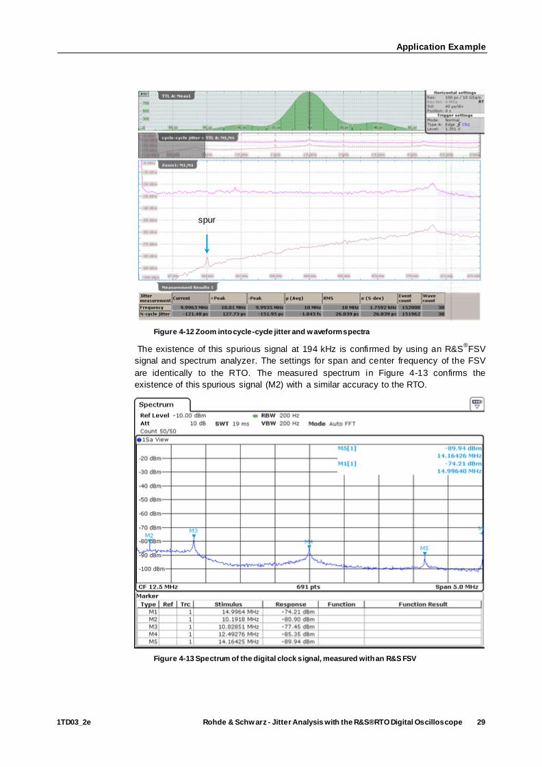
The comparison of both spectra demonstrates the benefit of a jitter spectrum. Looking
more closely into the spectra (see Figure 4-12) by using the zoom function of the RTO,
a spurious signal close to zero can be detected at 194 kHz within the jitter spectrum.
This spur is not visible within the waveform spectrum.
Application Example
1TD03_2e Rohde & Schwarz - Jitter Analysis with the R&S®RTO Digital Oscilloscope 29
Figure 4-12 Zoom into cycle-cycle jitter and waveform spectra
The existence of this spurious signal at 194 kHz is confirmed by using an R&S®FSV
signal and spectrum analyzer. The settings for span and center frequency of the FSV
are identically to the RTO. The measured spectrum in Figure 4-13 confirms the
existence of this spurious signal (M2) with a similar accuracy to the RTO.
Figure 4-13 Spectrum of the digital clock signal, measured with an R&S FSV
spur

Application Example
1TD03_2e Rohde & Schwarz - Jitter Analysis with the R&S®RTO Digital Oscilloscope 30
The RTO’s cycle-cycle jitter spectrum has a specific advantage over the RTO’s
associated spectrum of the waveform. This spectrum is able to resolve spurious
signals close to the carrier, which a spectrum of the waveform cannot display. The jitter
spectrum gives a good qualitative result, though the user should be careful using the
results for a quantitative analysis.
For completeness, Figure 4-14 presents an example with a N-cycle jitter measurement.
In the "Meas" menu > "Setup" tab, the user can change the "Cycle offset" to 4 from the
existing configuration. As a result, the PDF and track do not change, and the spectrum
looks similar to the one for the cycle-cycle jitter measurement. However, the zeros in
the spectrum are noticeable changed, which is caused by the transfer function of the
N-cycle jitter.
Figure 4-14 N-cycle jitter (N=4)
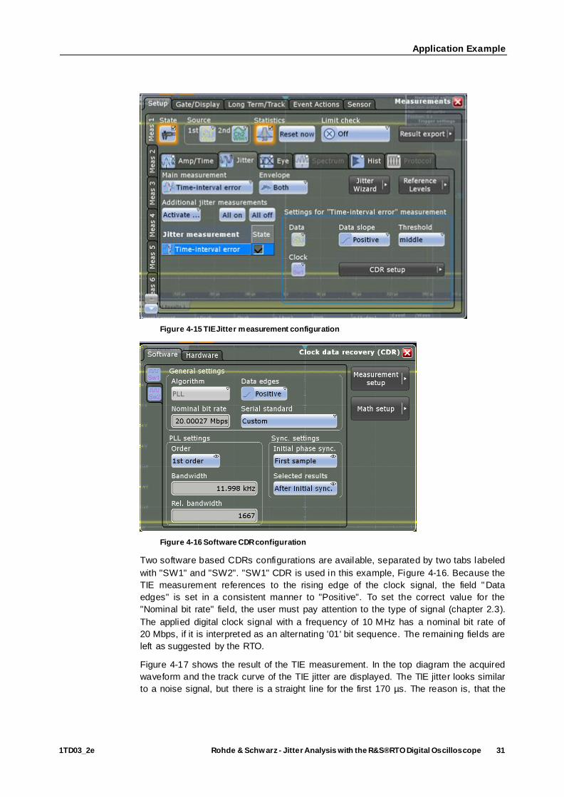
4.4 TIE Jitter Measurement
Chapter 3.3 introduced the TIE jitter and the respective measurement algorithm. The
TIE jitter measurement requires the configuration of the CDR in addition to the
configuration of the measurement. The following section explains both configurations.
Starting from the previous configuration, the user finds the TIE measurement in the
"Meas" menu > "Setup" tab > "Main measurement". Once the user has selected TIE
measurement, more user settings appear in the tab, Figure 4-15. A digital clock signal
usually strobes on the rising edge, so the "Data slope" field is set to "Positive". As the
TIE measurement requires a clock signal, the clock mode is set to "Software CDR".
The “CDR setup” button will get the user to the CDR configuration. Alternatively, the
user might select the configuration menu from the "Protocol" menu > "CDR Setup" >
"SW".
Application Example
1TD03_2e Rohde & Schwarz - Jitter Analysis with the R&S®RTO Digital Oscilloscope 31
Figure 4-15 TIE Jitter measurement configuration
Figure 4-16 Software CDR configuration
Two software based CDRs configurations are available, separated by two tabs labeled
with "SW1" and "SW2". "SW1" CDR is used in this example, Figure 4-16. Because the
TIE measurement references to the rising edge of the clock signal, the field "Data
edges" is set in a consistent manner to "Positive". To set the correct value for the
"Nominal bit rate" field, the user must pay attention to the type of signal (chapter 2.3).
The applied digital clock signal with a frequency of 10 MHz has a nominal bit rate of
20 Mbps, if it is interpreted as an alternating '01' bit sequence. The remaining fields are
left as suggested by the RTO.
Figure 4-17 shows the result of the TIE measurement. In the top diagram the acquired
waveform and the track curve of the TIE jitter are displayed. The TIE jitter looks similar
to a noise signal, but there is a straight line for the first 170 µs. The reason is, that the

Application Example
1TD03_2e Rohde & Schwarz - Jitter Analysis with the R&S®RTO Digital Oscilloscope 32
software based PLL, which starts over with every acquisition, must settle before it
provides a stable reference. During this settling time, the TIE jitter is set to a constant
value and therefore appears as a straight line. This behavior can be change d in the
CDR setup by setting the "Selected results" field from "After initial sync." to "All". Now
the TIE does not show an initial constant value, but the settling of the reference
falsifies this part of the track. A hardware based CDR does not start over and would
not show this behavior.
The second diagram shows the histogram of the TIE jitter with the PDF of the phase
noise function centered on the origin. As opposed to the period jitter the distribution
has changed to a bi-modal distribution with two peaks at ±20 ps.
The table at the bottom of the display shows the statistical data, as discussed in
chapter 2.3.1, for frequency TIE jitter measurement.
Figure 4-17 TIE jitter
To explore the change in the PDF from the period jitter to TIE jitter, the waveform is
minimized and the track curve is zoomed in Figure 4-18. A comparison of this track
with the track of the period jitter in Figure 4-8 shows that the disturbing signal is low
pass filtered. Without going into the mathematical analysis, a brief explanation shall be
provided in the following. The t ransfer function of a TIE measurement using a 1st
order
CDR exhibits the behavior of a low pass filter, which attenuates the DC components in
the phase noise signal. So the Dirac pulse t rain visible in the track curve in Figure 4-8,
is tuned into a '01' sequence, Figure 4-18, which has still a 40 ps change for the rising
and falling edges, but not from the 0 ps level anymore.

Application Example
1TD03_2e Rohde & Schwarz - Jitter Analysis with the R&S®RTO Digital Oscilloscope 33
Figure 4-18 TIE jitter zoomed
In the same way as in Figure 4-10, the spectrum is configured for TIE measurement
and associated waveform. In the top diagram Figure 4-19 displays the histogram and
in the second diagram the spectra of the TIE jitter (brown) and of the waveform
(magenta) with the same scale for both spectra. The congruence between both is
noticeable. Comparing the spectra of TIE jitter with the period jitter, the TIE jitter does
not show the attenuation towards the origin.
Figure 4-19 TIE jitter spectrum

Conclusion
1TD03_2e Rohde & Schwarz - Jitter Analysis with the R&S®RTO Digital Oscilloscope 34
5 Conclusion
For the transmission of signals, jitter is a significant limitation, which requires analysis
and characterization; this applies to system-level, board-level and chip-level. The RTO
in combination with the RTO-K12 option is a valuable tool, which offers a
comprehensive set of functions for the jitter analysis in design, debug and
conformance test of electronic circuits.
This application note discusses the measurement of period, cycle-cycle and TIE jitter
based on an application example and compares the impact on track, histogram and
spectrum display. It can be concluded that period measurements are most suitable for
oscillators, cycle-cycle measurements most applicable for PLLs and TIE
measurements most appropriate for transmitted data.
Low intrinsic jitter of the oscilloscope is a key parameter for a precise jitter
measurement. The excellent hardware of the RTO and the features of the RTO-K12
greatly support precise jitter analysis and allow remarkable detection capability. An
example is the detection of spurious signals close to a carrier.
The Jitter Wizard of the RTO-K12 offers an easy starting point for users of any
experience levels.
The R&S®RTO-K13 Clock Data Recovery option provides a unique and powerful
solution for eye-pattern analysis of binary data signals with an embedded c lock, which
gives extra value to the jitter analysis functions discussed in this application note.

Literature
1TD03_2e Rohde & Schwarz - Jitter Analysis with the R&S®RTO Digital Oscilloscope 35
6 Literature
1. R&S®FSUP Signal Source Analyzer Specifications. 81671 München, Germany :
Rohde & Schwarz GmbH & Co. KG, 2011.
2. Definition and terminology for synchronization net works. Geneve : ITU-T, 1996.
G.810.
3. Li, Mike Peng. Jitter, Noise, and Signal Integrity at High-Speed. s.l. : Prentice Hall,
2007.
4. Time Jitter and Phase Noise – Now and in the Future? Underhill, Michael J.
Lingfield, UK : IEEE, 2012.
5. Rice, John A. Mathematical Statistics and Data Analysis. Belmont, CA : Thomson,
2007.
6. Clock Jitter Estimation based on PM Noise Measurements. D. A. Howe; T. N.
Tasset. Boulder, CO 80305 : Proceedings of the 2003 IEEE International Frequency
Control Symposium, 2003.
7. Discrete-time signal processing. Alan V. Oppenheim, Ronald W. Schafer. s.l. :
Prentice Hall, 1989.
8. Spectral Analysis of Time-Domain Phase Jitter Measurements. Un-Ku Moon, Karti
Mayaram, John T. Stonick. 5, MAY 2002, IEEE TRANSACTIONS ON CIRCUITS
AND SYSTEMS—II: ANALOG AND DIGITAL SIGNAL PROCESSING, Bd. 49, S. 321-
327.
9. Definitions Of Jitter Measurement Terms And Relationships. Iliya Zamek Steve,
Zamek. s.l. : IEEE, 2005. INTERNATIONAL TEST CONFERENCE.

Ordering Information
1TD03_2e Rohde & Schwarz - Jitter Analysis with the R&S®RTO Digital Oscilloscope 36
7 Ordering Information
Naming Type Order number
Digital Oscilloscopes
600 MHz, 2 channels
10 Gsample/s, 20/40 Msample R&S®RTO1002 1316.1000.02
600 MHz, 4 channels
10 Gsample/s, 20/40 Msample R&S®RTO1004 1316.1000.04
1 GHz, 2 channels
10 Gsample/s, 20/40 Msample R&S®RTO1012 1316.1000.12
1 GHz, 4 channels
10 Gsample/s, 20/80 Msample R&S®RTO1014 1316.1000.14
2 GHz, 2 channels
10 Gsample/s, 20/40 Msample R&S®RTO1022 1316.1000.22
2 GHz, 4 channels
10 Gsample/s, 20/80 Msample R&S®RTO1024 1316.1000.24
4 GHz, 4 channels
20 Gsample/s, 20/80 Msample R&S®RTO1044 1316.1000.44
Software Options
Jitter analysis option R&S®RTO-K12 1317.4690.02
CDR option R&S®RTO-K13 1317.4703.02

About Rohde & Schwarz
Rohde & Schwarz is an independent group of
companies specializing in electronics. It is a leading
supplier of solutions in the fields of test and
measurement, broadcasting, radiomonitoring and
radiolocation, as well as secure communications.
Established more than 75 years ago, Rohde &
Schwarz has a global presence and a dedicated
service network in over 70 countries. Company
headquarters are in Munich, Germany.
Regional contact
Europe, Africa, Middle East +49 89 4129 12345 [email protected]
North America 1-888-TEST-RSA (1-888-837-8772)
[email protected] Latin America
+1-410-910-7988 [email protected]
Asia/Pacific +65 65 13 04 88 [email protected]
China +86-800-810-8228 /+86-400-650-5896 [email protected]
Environmental commitment
ı Energy-efficient products
ı Continuous improvement in environmental
sustainability
ı ISO 14001-certi fied environmental
management system
This and the supplied programs may only be used
subject to the conditions of use set forth in the
download area of the Rohde & Schwarz website.
R&S® is a registered trademark of Rohde & Schwarz GmbH & Co.
KG; Trade names are trademarks of the ow ners.
Rohde & Schwarz GmbH & Co. KG
Mühldorfstraße 15 | D - 81671 München
Phone + 49 89 4129 - 0 | Fax + 49 89 4129 – 13777
www.rohde-schwarz.com
PA
D-T
-M: 3573
.7380.0
2/0
2.0
0/C
I/1/
EN
/