Embed Size (px)
Citation preview

JDK.F98 Slide 1
Lecture 2: Review of Instruction Sets, Pipelines,
and Caches
Prof. John Kubiatowicz
Computer Science 252
Fall 1998

JDK.F98 Slide 2
Review, #1• Technology is changing rapidly:
Capacity Speed
Logic 2x in 3 years 2x in 3 years
DRAM 4x in 3 years 2x in 10 years
Disk 4x in 3 years 2x in 10 years
Processor ( n.a.) 2x in 1.5 years
• What was true five years ago is not necessarily true now.
• Execution time is the REAL measure of computer performance!– Not clock rate, not CPI
• “X is n times faster than Y” means:
e(Y)Performance(X)Performanc
ExTime(X)ExTime(y)
JDK.F98 Slide 3
Review, #2• Amdahl’s Law: (or Law of Diminishing
Returns)
• CPI Law:
• The “End to End Argument” is what RISC was ultimately about -- it is the performance of the complete system that matters, not individual components!
CPU time = Seconds = Instructions x Cycles x Seconds
Program Program Instruction Cycle
CPU time = Seconds = Instructions x Cycles x Seconds
Program Program Instruction Cycle
enhanced
enhancedenhanced
new
oldoverall
Speedup
Fraction Fraction
1
ExTimeExTime
Speedup
1

JDK.F98 Slide 4
Today: Quick review of everything you should have learned
0
( A countably-infinite set of computer architecture
concepts )

JDK.F98 Slide 5
Integrated Circuits Costs
Die Cost goes roughly with die area4
Test_Die Die_Area 2
Wafer_diam
Die_Area
2m/2)(Wafer_dia wafer per Dies
Die_area sityDefect_Den
1 dWafer_yiel YieldDie
yieldtest Finalcost Packaging cost Testingcost Die
cost IC
yield Die Wafer per DiescostWafer
cost Die
JDK.F98 Slide 6
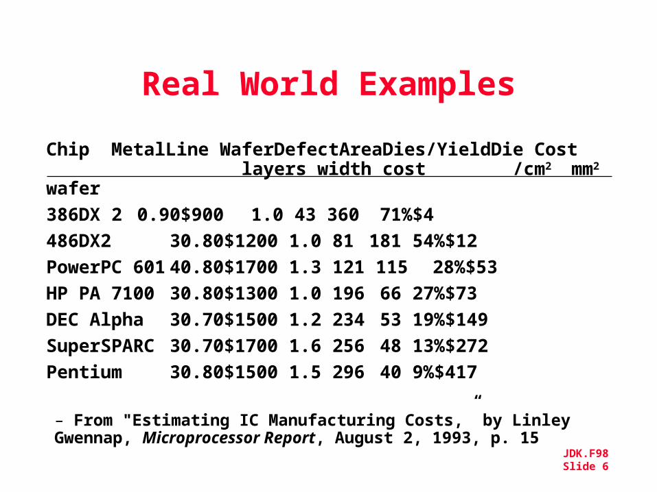
Real World Examples
Chip Metal Line Wafer Defect Area Dies/ Yield Die Cost layers width cost /cm2 mm2 wafer
386DX 2 0.90 $900 1.0 43 360 71% $4
486DX2 3 0.80 $1200 1.0 81 181 54% $12
PowerPC 601 4 0.80 $1700 1.3 121 115 28% $53
HP PA 7100 3 0.80 $1300 1.0 196 66 27% $73
DEC Alpha 3 0.70 $1500 1.2 234 53 19% $149
SuperSPARC 3 0.70 $1700 1.6 256 48 13% $272
Pentium 3 0.80 $1500 1.5 296 40 9% $417
– From "Estimating IC Manufacturing Costs,” by Linley Gwennap, Microprocessor Report, August 2, 1993, p. 15

JDK.F98 Slide 7
Finite State Machines:• System state is explicit in representation• Transitions between states represented as
arrows with inputs on arcs.• Output may be either part of state or on arcs
Alpha/
0
Delta/
2
Beta/
10
1
1
0
0
1
“Mod 3 Machine”
Input (MSB first)
0 1 0 1 00 1 2 2
1
106
Mod 3
1
1
1 1
0

JDK.F98 Slide 8
“M
eale
y M
ach
ine”“M
oore
Mach
ine”
Implementation as Combinational logic +
LatchAlpha/
0
Delta/
2
Beta/
10/0
1/0
1/1
0/10/0
1/1
Latc
h
Com
bin
ati
on
al
Log
ic
I nput Stateold Statenew Div
000
000110
001001
001
111
000110
010010
011

JDK.F98 Slide 9
Microprogrammed Controllers
• State machine in which part of state is a “micro-pc”.– Explicit circuitry for incrementing or changing PC
• Includes a ROM with “microinstructions”.– Controlled logic implements at least branches and jumps
RO
M(In
stru
ctio
ns)
Addr
BranchPC
+ 1
MUX
Next Address
Control
0: forw 35 xxx1: b_no_obstacles 0002: back 10 xxx3: rotate 90 xxx4: goto 001
Instruction Branch
Com
bin
ati
on
al Log
ic/
Con
trolled
Mach
ineS
tate
w/ A
dd
ress

JDK.F98 Slide 10
Pipelining: Its Natural!
• Laundry Example• Ann, Brian, Cathy, Dave
each have one load of clothes to wash, dry, and fold
• Washer takes 30 minutes
• Dryer takes 40 minutes
• “Folder” takes 20 minutes
A B C D

JDK.F98 Slide 11
Sequential Laundry
• Sequential laundry takes 6 hours for 4 loads• If they learned pipelining, how long would laundry take?
A
B
C
D
30 40 2030 40 2030 40 2030 40 20
6 PM 7 8 9 10 11 Midnight
Task
Order
Time

JDK.F98 Slide 12
Pipelined LaundryStart work ASAP
• Pipelined laundry takes 3.5 hours for 4 loads
A
B
C
D
6 PM 7 8 9 10 11 Midnight
Task
Order
Time
30 40 40 40 40 20

JDK.F98 Slide 13
Pipelining Lessons• Pipelining doesn’t help
latency of single task, it helps throughput of entire workload
• Pipeline rate limited by slowest pipeline stage
• Multiple tasks operating simultaneously
• Potential speedup = Number pipe stages
• Unbalanced lengths of pipe stages reduces speedup
• Time to “fill” pipeline and time to “drain” it reduces speedup
A
B
C
D
6 PM 7 8 9
Task
Order
Time
30 40 40 40 40 20

JDK.F98 Slide 14
Computer Pipelines
• Execute billions of instructions, so throughput is what matters
• DLX desirable features: all instructions same length, registers located in same place in instruction format, memory operands only in loads or stores

JDK.F98 Slide 15
A "Typical" RISC
• 32-bit fixed format instruction (3 formats)• 32 32-bit GPR (R0 contains zero, DP take
pair)• 3-address, reg-reg arithmetic instruction• Single address mode for load/store:
base + displacement– no indirection
• Simple branch conditions• Delayed branch
see: SPARC, MIPS, HP PA-Risc, DEC Alpha, IBM PowerPC, CDC 6600, CDC 7600, Cray-1, Cray-2, Cray-3

JDK.F98 Slide 16
Example: MIPS ( DLX)
Op
31 26 01516202125
Rs1 Rd immediate
Op
31 26 025
Op
31 26 01516202125
Rs1 Rs2
target
Rd Opx
Register-Register
561011
Register-Immediate
Op
31 26 01516202125
Rs1 Rs2/Opx immediate
Branch
Jump / Call

JDK.F98 Slide 17
5 Steps of DLX DatapathFigure 3.1, Page 130
MemoryAccess
Write
Back
InstructionFetch
Instr. DecodeReg. Fetch
ExecuteAddr. Calc
LMD
ALU
MU
X
Mem
ory
Reg File
MU
XM
UX
Data
Mem
ory
MU
X
SignExtend
4
Ad
der Zero?
Next SEQ PC
Addre
ss
Next PC
WB Data
Inst
RD
RS1
RS2
Imm

JDK.F98 Slide 18
5 Steps of DLX DatapathFigure 3.4, Page 137
MemoryAccess
Write
Back
InstructionFetch
Instr. DecodeReg. Fetch
ExecuteAddr. Calc
ALU
Mem
ory
Reg File
MU
XM
UX
Data
Mem
ory
MU
X
SignExtend
Zero?
IF/ID
ID/E
X
MEM
/WB
EX
/MEM
4
Ad
der
Next SEQ PC Next SEQ PC
RD RD RD WB
Data
• Data stationary control– local decode for each instruction phase / pipeline stage
Next PC
Addre
ss
RS1
RS2
Imm
MU
X

JDK.F98 Slide 19
Visualizing PipeliningFigure 3.3, Page 133
Instr.
Order
Time (clock cycles)
Reg
ALU
DMemIfetch Reg
Reg
ALU
DMemIfetch Reg
Reg
ALU
DMemIfetch Reg
Reg
ALU
DMemIfetch Reg
Cycle 1Cycle 2 Cycle 3Cycle 4 Cycle 6Cycle 7Cycle 5

JDK.F98 Slide 20
Its Not That Easy for Computers
• Limits to pipelining: Hazards prevent next instruction from executing during its designated clock cycle
– Structural hazards: HW cannot support this combination of instructions (single person to fold and put clothes away)
– Data hazards: Instruction depends on result of prior instruction still in the pipeline (missing sock)
– Control hazards: Caused by delay between the fetching of instructions and decisions about changes in control flow (branches and jumps).

JDK.F98 Slide 21
One Memory Port/Structural Hazards
Figure 3.6, Page 142
Instr.
Order
Time (clock cycles)
Load
Instr 1
Instr 2
Instr 3
Instr 4
Reg
ALU
DMemIfetch Reg
Reg
ALU
DMemIfetch Reg
Reg
ALU
DMemIfetch Reg
Reg
ALU
DMemIfetch Reg
Cycle 1Cycle 2 Cycle 3Cycle 4 Cycle 6Cycle 7Cycle 5
Reg
ALU
DMemIfetch Reg
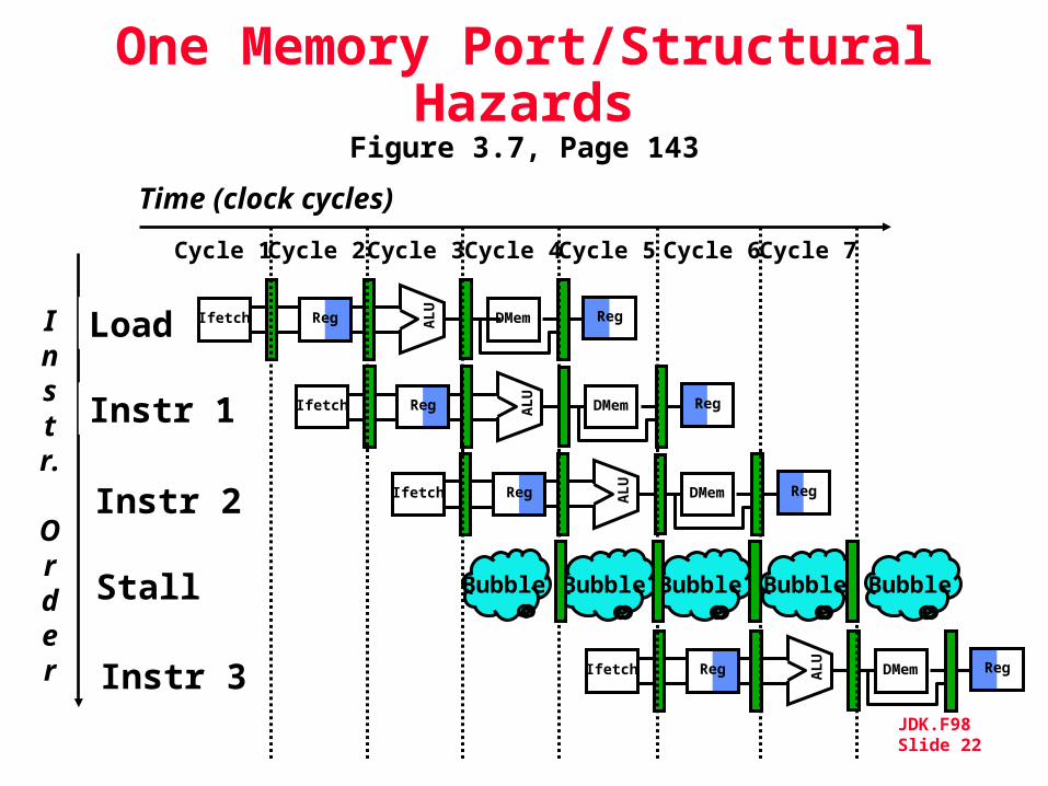
JDK.F98 Slide 22
One Memory Port/Structural Hazards
Figure 3.7, Page 143
Instr.
Order
Time (clock cycles)
Load
Instr 1
Instr 2
Stall
Instr 3
Reg
ALU
DMemIfetch Reg
Reg
ALU
DMemIfetch Reg
Reg
ALU
DMemIfetch Reg
Cycle 1Cycle 2 Cycle 3Cycle 4 Cycle 6Cycle 7Cycle 5
Reg
ALU
DMemIfetch Reg
Bubble Bubble Bubble BubbleBubble

JDK.F98 Slide 23
Speed Up Equation for Pipelining
pipelined
dunpipeline
TimeCycle
TimeCycle
CPI stall Pipeline CPI Idealdepth Pipeline CPI Ideal
Speedup
pipelined
dunpipeline
TimeCycle
TimeCycle
CPI stall Pipeline 1depth Pipeline
Speedup
Instper cycles Stall Average CPI Ideal CPIpipelined
For simple RISC pipeline, CPI = 1:

JDK.F98 Slide 24
Example: Dual-port vs. Single-port
• Machine A: Dual ported memory (“Harvard Architecture”)
• Machine B: Single ported memory, but its pipelined implementation has a 1.05 times faster clock rate
• Ideal CPI = 1 for both• Loads are 40% of instructions executed
SpeedUpA = Pipeline Depth/(1 + 0) x (clockunpipe/clockpipe)
= Pipeline Depth
SpeedUpB = Pipeline Depth/(1 + 0.4 x 1) x (clockunpipe/(clockunpipe / 1.05)
= (Pipeline Depth/1.4) x 1.05
= 0.75 x Pipeline Depth
SpeedUpA / SpeedUpB = Pipeline Depth/(0.75 x Pipeline Depth) = 1.33
• Machine A is 1.33 times faster

JDK.F98 Slide 25
Instr.
Order
add r1,r2,r3
sub r4,r1,r3
and r6,r1,r7
or r8,r1,r9
xor r10,r1,r11
Reg
ALU
DMemIfetch Reg
Reg
ALU
DMemIfetch Reg
Reg
ALU
DMemIfetch Reg
Reg
ALU
DMemIfetch Reg
Reg
ALU
DMemIfetch Reg
Data Hazard on R1Figure 3.9, page 147
Time (clock cycles)
IF ID/RF EX MEM WB

JDK.F98 Slide 26
Three Generic Data Hazards
• Read After Write (RAW) InstrJ tries to read operand before InstrI writes it
• Caused by a “Dependence” (in compiler nomenclature). This hazard results from an actual need for communication.
I: add r1,r2,r3J: sub r4,r1,r3

JDK.F98 Slide 27
• Write After Read (WAR) InstrJ writes operand before InstrI reads it
• Called an “anti-dependence” by compiler writers.This results from reuse of the name “r1”.
• Can’t happen in DLX 5 stage pipeline because:– All instructions take 5 stages, and– Reads are always in stage 2, and – Writes are always in stage 5
I: sub r4,r1,r3 J: add r1,r2,r3K: mul r6,r1,r7
Three Generic Data Hazards

JDK.F98 Slide 28
Three Generic Data Hazards
• Write After Write (WAW) InstrJ writes operand before InstrI writes it.
• Called an “output dependence” by compiler writersThis also results from the reuse of name “r1”.
• Can’t happen in DLX 5 stage pipeline because: – All instructions take 5 stages, and – Writes are always in stage 5
• Will see WAR and WAW in later more complicated pipes
I: sub r1,r4,r3 J: add r1,r2,r3K: mul r6,r1,r7

JDK.F98 Slide 29
CS 252 Administrivia
• Sign up today! Web site is: http://www.cs.berkeley.edu/~kubitron/cs252-F98
• In class exam on Wednesday Sept 2nd– Improve 252 experience if recapture common background– Bring 1 sheet of paper with notes on both sides– Doesn’t affect grade, only admission into class– 2 grades: Admitted or audit/take CS 152 1st (before class Friday)
• Review: Chapters 1- 3, CS 152 home page, maybe “Computer Organization and Design (COD)2/e”
– If did take a class, be sure COD Chapters 2, 5, 6, 7 are familiar– Copies in Bechtel Library on 2-hour reserve
• Aaron Brown will be holding a review session this weekend: Sunday, Aug 30. 1:00pm. 310 Soda

JDK.F98 Slide 30
CS 252 Administrivia• Resources for course on web site:
– Check out the ISCA (International Symposium on Computer Architecture) 25th year retrospective on web site.Look for “Additional reading” below text-book description
– Pointers to previous CS152 exams and resources– Lots of old CS252 material– Interesting pointers at bottom. Check out the:
WWW Computer Architecture Home Page
• To give proper attention to projects (as well as homeworks and quizes), I can handle up to 36 students
– First priority is students taking ARCH prelims in next year– Second priority is students taking this for breadth– Third priority is EECS students– Fourth priority College of Engineering grad students

JDK.F98 Slide 31
Time (clock cycles)
Forwarding to Avoid Data Hazard
Figure 3.10, Page 149
Inst
r.
Order
add r1,r2,r3
sub r4,r1,r3
and r6,r1,r7
or r8,r1,r9
xor r10,r1,r11
Reg
ALU
DMemIfetch Reg
Reg
ALU
DMemIfetch Reg
Reg
ALU
DMemIfetch Reg
Reg
ALU
DMemIfetch Reg
Reg
ALU
DMemIfetch Reg

JDK.F98 Slide 32
HW Change for ForwardingFigure 3.20, Page 161

JDK.F98 Slide 33
Time (clock cycles)
Instr.
Order
lw r1, 0(r2)
sub r4,r1,r6
and r6,r1,r7
or r8,r1,r9
Data Hazard Even with Forwarding
Figure 3.12, Page 153
Reg
ALU
DMemIfetch Reg
Reg
ALU
DMemIfetch Reg
Reg ALU
DMemIfetch Reg
Reg
ALU
DMemIfetch Reg

JDK.F98 Slide 34
Data Hazard Even with ForwardingFigure 3.13, Page 154
Time (clock cycles)
or r8,r1,r9
Instr.
Order
lw r1, 0(r2)
sub r4,r1,r6
and r6,r1,r7
Reg
ALU
DMemIfetch Reg
RegIfetch
ALU
DMem RegBubble
Ifetch
ALU
DMem RegBubble Reg
Ifetch
ALU
DMemBubble Reg

JDK.F98 Slide 35
Try producing fast code for
a = b + c;
d = e – f;
assuming a, b, c, d ,e, and f in memory. Slow code:
LW Rb,b
LW Rc,c
ADD Ra,Rb,Rc
SW a,Ra
LW Re,e
LW Rf,f
SUB Rd,Re,Rf
SW d,Rd
Software Scheduling to Avoid Load Hazards
Fast code:
LW Rb,b
LW Rc,c
LW Re,e
ADD Ra,Rb,Rc
LW Rf,f
SW a,Ra
SUB Rd,Re,Rf
SW d,Rd

JDK.F98 Slide 36
Control Hazard on Branches
Three Stage Stall
10: beq r1,r3,36
14: and r2,r3,r5
18: or r6,r1,r7
22: add r8,r1,r9
36: xor r10,r1,r11
Reg ALU
DMemIfetch Reg
Reg
ALU
DMemIfetch Reg
Reg
ALU
DMemIfetch Reg
Reg
ALU
DMemIfetch Reg
Reg
ALU
DMemIfetch Reg

JDK.F98 Slide 37
Branch Stall Impact
• If CPI = 1, 30% branch, Stall 3 cycles => new CPI = 1.9!
• Two part solution:– Determine branch taken or not sooner, AND– Compute taken branch address earlier
• DLX branch tests if register = 0 or • 0• DLX Solution:
– Move Zero test to ID/RF stage– Adder to calculate new PC in ID/RF stage– 1 clock cycle penalty for branch versus 3

JDK.F98 Slide 38
Pipelined DLX DatapathFigure 3.22, page 163
MemoryAccess
WriteBack
InstructionFetch
Instr. DecodeReg. Fetch
ExecuteAddr. Calc.
This is the correct 1 cyclelatency implementation!

JDK.F98 Slide 39
Four Branch Hazard Alternatives
#1: Stall until branch direction is clear
#2: Predict Branch Not Taken– Execute successor instructions in sequence– “Squash” instructions in pipeline if branch actually taken– Advantage of late pipeline state update– 47% DLX branches not taken on average– PC+4 already calculated, so use it to get next instruction
#3: Predict Branch Taken– 53% DLX branches taken on average– But haven’t calculated branch target address in DLX
» DLX still incurs 1 cycle branch penalty» Other machines: branch target known before outcome

JDK.F98 Slide 40
Four Branch Hazard Alternatives
#4: Delayed Branch– Define branch to take place AFTER a following instruction
branch instructionsequential successor1
sequential successor2
........sequential successorn
branch target if taken
– 1 slot delay allows proper decision and branch target address in 5 stage pipeline
– DLX uses this
Branch delay of length n

JDK.F98 Slide 41
Delayed Branch
• Where to get instructions to fill branch delay slot?– Before branch instruction– From the target address: only valuable when branch taken– From fall through: only valuable when branch not taken– Cancelling branches allow more slots to be filled
• Compiler effectiveness for single branch delay slot:– Fills about 60% of branch delay slots– About 80% of instructions executed in branch delay slots useful in
computation– About 50% (60% x 80%) of slots usefully filled
• Delayed Branch downside: 7-8 stage pipelines, multiple instructions issued per clock (superscalar)

JDK.F98 Slide 42
Evaluating Branch Alternatives
Scheduling Branch CPIspeedup v.speedup v. scheme penalty unpipelined stall
Stall pipeline 3 1.42 3.51.0
Predict taken 1 1.14 4.41.26
Predict not taken 1 1.09 4.51.29
Delayed branch 0.5 1.07 4.61.31
Conditional & Unconditional = 14%, 65% change PC
Pipeline speedup = Pipeline depth1 +Branch frequencyBranch penalty

JDK.F98 Slide 43
Now, Review of Memory Hierarchy

JDK.F98 Slide 44
Recap: Who Cares About the Memory Hierarchy?
µProc60%/yr.(2X/1.5yr)
DRAM9%/yr.(2X/10 yrs)
1
10
100
1000
198
0198
1 198
3198
4198
5 198
6198
7198
8198
9199
0199
1 199
2199
3199
4199
5199
6199
7199
8 199
9200
0
DRAM
CPU198
2
Processor-MemoryPerformance Gap:(grows 50% / year)
Perf
orm
an
ce
Time
“Moore’s Law”
Processor-DRAM Memory Gap (latency)

JDK.F98 Slide 45
Levels of the Memory Hierarchy
CPU Registers100s Bytes<10s ns
CacheK Bytes10-100 ns1-0.1 cents/bit
Main MemoryM Bytes200ns- 500ns$.0001-.00001 cents /bit
DiskG Bytes, 10 ms (10,000,000 ns)
10 - 10 cents/bit-5 -6
CapacityAccess TimeCost
Tapeinfinitesec-min10 -8
Registers
Cache
Memory
Disk
Tape
Instr. Operands
Blocks
Pages
Files
StagingXfer Unit
prog./compiler1-8 bytes
cache cntl8-128 bytes
OS512-4K bytes
user/operatorMbytes
Upper Level
Lower Level
faster
Larger

JDK.F98 Slide 46
The Principle of Locality
• The Principle of Locality:– Program access a relatively small portion of the address space at any
instant of time.
• Two Different Types of Locality:– Temporal Locality (Locality in Time): If an item is referenced, it will tend
to be referenced again soon (e.g., loops, reuse)– Spatial Locality (Locality in Space): If an item is referenced, items whose
addresses are close by tend to be referenced soon (e.g., straightline code, array access)
• Last 15 years, HW relied on localilty for speed

JDK.F98 Slide 47
Memory Hierarchy: Terminology
• Hit: data appears in some block in the upper level (example: Block X)
– Hit Rate: the fraction of memory access found in the upper level– Hit Time: Time to access the upper level which consists of
RAM access time + Time to determine hit/miss
• Miss: data needs to be retrieve from a block in the lower level (Block Y)
– Miss Rate = 1 - (Hit Rate)– Miss Penalty: Time to replace a block in the upper level +
Time to deliver the block the processor
• Hit Time << Miss Penalty (500 instructions on 21264!)
Lower LevelMemoryUpper Level
MemoryTo Processor
From ProcessorBlk X
Blk Y

JDK.F98 Slide 48
Cache Measures
• Hit rate: fraction found in that level– So high that usually talk about Miss rate– Miss rate fallacy: as MIPS to CPU performance,
miss rate to average memory access time in memory
• Average memory-access time = Hit time + Miss rate x Miss penalty
(ns or clocks)• Miss penalty: time to replace a block from
lower level, including time to replace in CPU– access time: time to lower level
= f(latency to lower level)
– transfer time: time to transfer block
=f(BW between upper & lower levels)

JDK.F98 Slide 49
Simplest Cache: Direct Mapped
Memory
4 Byte Direct Mapped Cache
Memory Address0
1
2
3
4
5
6
7
8
9
A
B
C
D
E
F
Cache Index
0
1
2
3• Location 0 can be occupied by data
from:– Memory location 0, 4, 8, ... etc.– In general: any memory location
whose 2 LSBs of the address are 0s– Address<1:0> => cache index
• Which one should we place in the cache?
• How can we tell which one is in the cache?

JDK.F98 Slide 50
1 KB Direct Mapped Cache, 32B blocks
• For a 2 ** N byte cache:– The uppermost (32 - N) bits are always the Cache Tag– The lowest M bits are the Byte Select (Block Size = 2 ** M)
Cache Index
0
1
2
3
:
Cache Data
Byte 0
0431
:
Cache Tag Example: 0x50
Ex: 0x01
0x50
Stored as partof the cache “state”
Valid Bit
:
31
Byte 1Byte 31 :
Byte 32Byte 33Byte 63 :Byte 992Byte 1023 :
Cache Tag
Byte Select
Ex: 0x00
9
JDK.F98 Slide 51
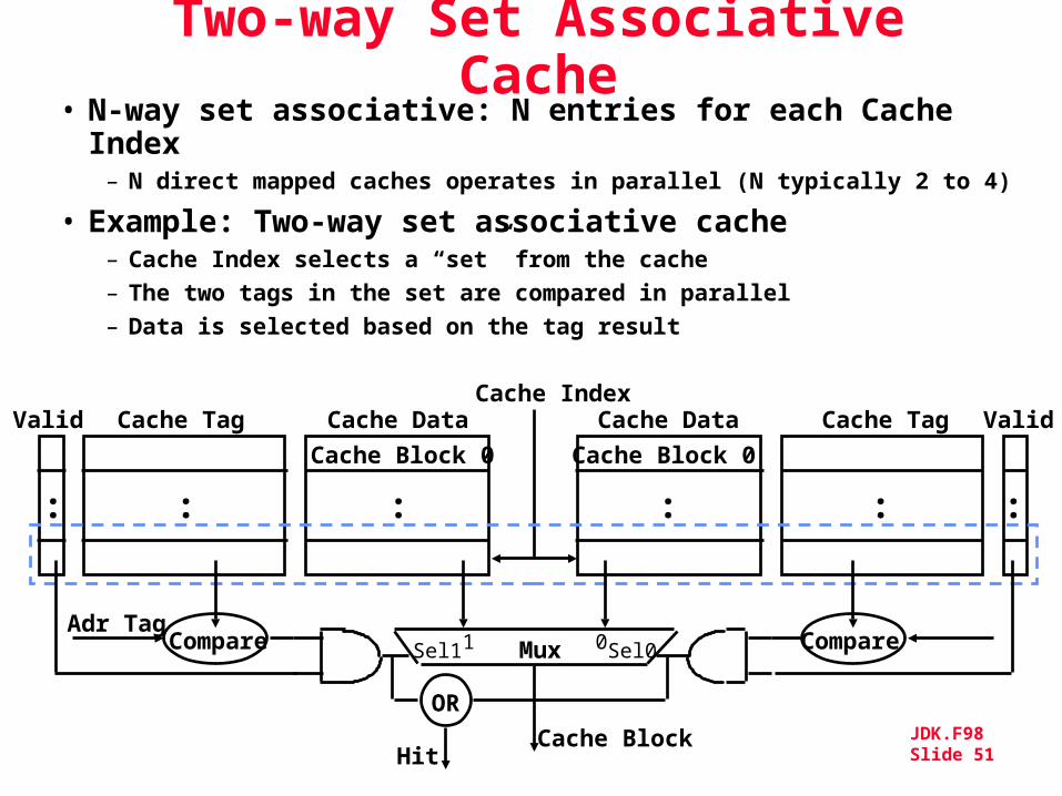
Two-way Set Associative Cache
• N-way set associative: N entries for each Cache Index
– N direct mapped caches operates in parallel (N typically 2 to 4)
• Example: Two-way set associative cache– Cache Index selects a “set” from the cache– The two tags in the set are compared in parallel– Data is selected based on the tag result
Cache Data
Cache Block 0
Cache TagValid
:: :
Cache Data
Cache Block 0
Cache Tag Valid
: ::
Cache Index
Mux 01Sel1 Sel0
Cache Block
CompareAdr Tag
Compare
OR
Hit

JDK.F98 Slide 52
Disadvantage of Set Associative Cache
• N-way Set Associative Cache v. Direct Mapped Cache:– N comparators vs. 1– Extra MUX delay for the data– Data comes AFTER Hit/Miss
• In a direct mapped cache, Cache Block is available BEFORE Hit/Miss:
– Possible to assume a hit and continue. Recover later if miss.
Cache Data
Cache Block 0
Cache Tag Valid
: ::
Cache Data
Cache Block 0
Cache TagValid
:: :
Cache Index
Mux 01Sel1 Sel0
Cache Block
CompareAdr Tag
Compare
OR
Hit

JDK.F98 Slide 53
4 Questions for Memory Hierarchy
• Q1: Where can a block be placed in the upper level? (Block placement)
• Q2: How is a block found if it is in the upper level? (Block identification)
• Q3: Which block should be replaced on a miss?
(Block replacement)• Q4: What happens on a write?
(Write strategy)

JDK.F98 Slide 54
Q1: Where can a block be placed in the upper level?
• Block 12 placed in 8 block cache:– Fully associative, direct mapped, 2-way set
associative– S.A. Mapping = Block Number Modulo Number
Sets
Cache
01234567 0123456701234567
Memory
111111111122222222223301234567890123456789012345678901
Full MappedDirect Mapped(12 mod 8) = 4
2-Way Assoc(12 mod 4) = 0

JDK.F98 Slide 55
Q2: How is a block found if it is in the upper level?
• Tag on each block– No need to check index or block offset
• Increasing associativity shrinks index, expands tag
BlockOffset
Block Address
IndexTag

JDK.F98 Slide 56
Q3: Which block should be replaced on a miss?
• Easy for Direct Mapped
• Set Associative or Fully Associative:– Random
– LRU (Least Recently Used)
Assoc: 2-way 4-way 8-way
Size LRU Ran LRU Ran LRU Ran
16 KB 5.2% 5.7% 4.7% 5.3% 4.4% 5.0%
64 KB 1.9% 2.0% 1.5% 1.7% 1.4% 1.5%
256 KB 1.15% 1.17% 1.13% 1.13% 1.12% 1.12%

JDK.F98 Slide 57
Q4: What happens on a write?
• Write through—The information is written to both the block in the cache and to the block in the lower-level memory.
• Write back—The information is written only to the block in the cache. The modified cache block is written to main memory only when it is replaced.
– is block clean or dirty?
• Pros and Cons of each?– WT: read misses cannot result in writes– WB: no repeated writes to same location
• WT always combined with write buffers so that don’t wait for lower level memory

JDK.F98 Slide 58
Write Buffer for Write Through
• A Write Buffer is needed between the Cache and Memory
– Processor: writes data into the cache and the write buffer– Memory controller: write contents of the buffer to memory
• Write buffer is just a FIFO:– Typical number of entries: 4– Works fine if: Store frequency (w.r.t. time) << 1 / DRAM write
cycle
• Memory system designer’s nightmare:– Store frequency (w.r.t. time) -> 1 / DRAM write cycle– Write buffer saturation
ProcessorCache
Write Buffer
DRAM

JDK.F98 Slide 59
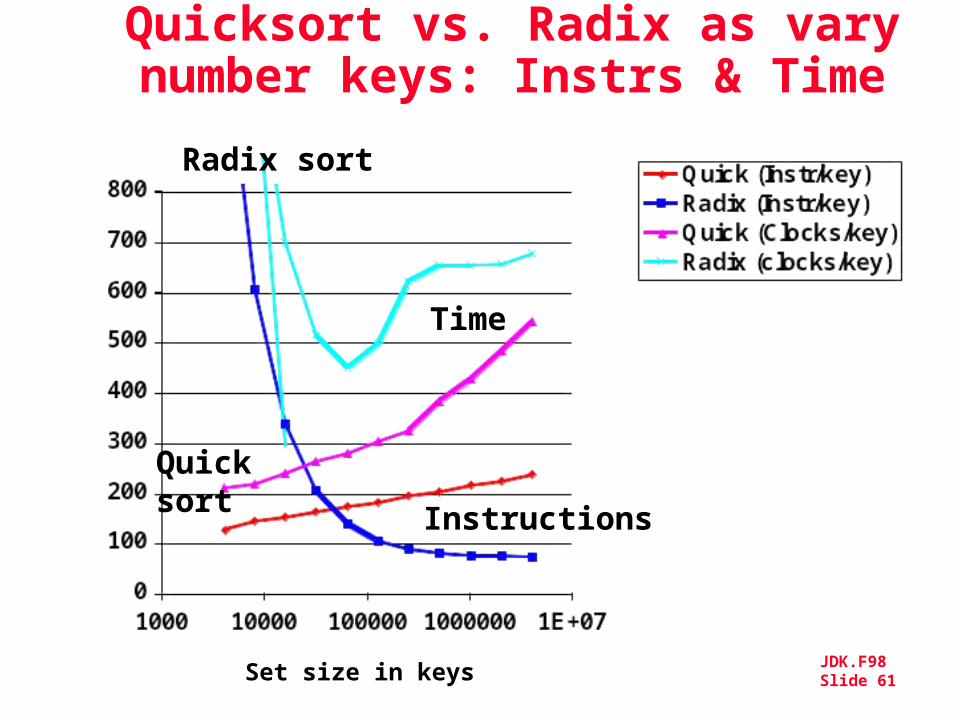
Impact of Memory Hierarchy on Algorithms
• Today CPU time is a function of (ops, cache misses) vs. just f(ops):What does this mean to Compilers, Data structures, Algorithms?
• “The Influence of Caches on the Performance of Sorting” by A. LaMarca and R.E. Ladner. Proceedings of the Eighth Annual ACM-SIAM Symposium on Discrete Algorithms, January, 1997, 370-379.
• Quicksort: fastest comparison based sorting algorithm when all keys fit in memory
• Radix sort: also called “linear time” sort because for keys of fixed length and fixed radix a constant number of passes over the data is sufficient independent of the number of keys
• For Alphastation 250, 32 byte blocks, direct mapped L2 2MB cache, 8 byte keys, from 4000 to 4000000

JDK.F98 Slide 60
Quicksort vs. Radix as vary number keys: Instructions
Set size in keys
Instructions/key
Radix sort
Quicksort
JDK.F98 Slide 61
Quicksort vs. Radix as vary number keys: Instrs & Time
Time
Set size in keys
Instructions
Radix sort
Quicksort

JDK.F98 Slide 62
Quicksort vs. Radix as vary number keys: Cache misses
Cache misses
Set size in keys
Radix sort
Quicksort
What is proper approach to fast algorithms?

JDK.F98 Slide 63
5 minute Class Break
• 80 minutes straight is too long for me to lecture (12:40:00 – 2:00:00):
– 1 minute: review last time & motivate this lecture
– 20 minute lecture– 3 minutes: discuss class manangement– 25 minutes: lecture – 5 minutes: break– 25 minutes: lecture– 1 minute: summary of today’s important
topics

JDK.F98 Slide 64
A Modern Memory Hierarchy
• By taking advantage of the principle of locality:– Present the user with as much memory as is available in the
cheapest technology.– Provide access at the speed offered by the fastest technology.
Control
Datapath
SecondaryStorage(Disk)
Processor
Registers
MainMemory(DRAM)
SecondLevelCache
(SRAM)
On
-Ch
ipC
ache
1s 10,000,000s (10s ms)
Speed (ns): 10s 100s
100sGs
Size (bytes):Ks Ms
TertiaryStorage
(Disk/Tape)
10,000,000,000s (10s sec)
Ts

JDK.F98 Slide 65
Basic Issues in VM System Design
size of information blocks that are transferred from secondary to main storage (M)
block of information brought into M, and M is full, then some region of M must be released to make room for the new block --> replacement policy
which region of M is to hold the new block --> placement policy
missing item fetched from secondary memory only on the occurrence of a fault --> demand load policy
Paging Organization
virtual and physical address space partitioned into blocks of equal size
page frames
pages
pagesreg
cachemem disk
frame

JDK.F98 Slide 66
Address MapV = {0, 1, . . . , n - 1} virtual address spaceM = {0, 1, . . . , m - 1} physical address space
MAP: V --> M U {0} address mapping function
n > m
MAP(a) = a' if data at virtual address a is present in physical address a' and a' in M
= 0 if data at virtual address a is not present in M
Processor
Name Space V
Addr TransMechanism
faulthandler
MainMemory
SecondaryMemory
a
aa'
0
missing item fault
physical address OS performsthis transfer

JDK.F98 Slide 67
Paging Organization
frame 01
7
01024
7168
P.A.
PhysicalMemory
1K1K
1K
AddrTransMAP
page 01
31
1K1K
1K
01024
31744
unit of mapping
also unit oftransfer fromvirtual tophysical memory
Virtual Memory
Address Mapping
VA page no. disp10
Page Table
indexintopagetable
Page TableBase Reg
V AccessRights PA +
table locatedin physicalmemory
physicalmemoryaddress
actually, concatenation is more likely
V.A.

JDK.F98 Slide 68
Virtual Address and a Cache
CPUTrans-lation
Cache MainMemory
VA PA miss
hitdata
It takes an extra memory access to translate VA to PA
This makes cache access very expensive, and this is the "innermost loop" that you want to go as fast as possible
ASIDE: Why access cache with PA at all? VA caches have a problem! synonym / alias problem: two different virtual addresses map to same physical address => two different cache entries holding data for the same physical address!
for update: must update all cache entries with same physical address or memory becomes inconsistent
determining this requires significant hardware, essentially an associative lookup on the physical address tags to see if you have multiple hits; or
software enforced alias boundary: same lsb of VA &PA > cache size

JDK.F98 Slide 69
TLBsA way to speed up translation is to use a special cache of recently used page table entries -- this has many names, but the most frequently used is Translation Lookaside Buffer or TLB
Virtual Address Physical Address Dirty Ref Valid Access
Really just a cache on the page table mappings
TLB access time comparable to cache access time (much less than main memory access time)

JDK.F98 Slide 70
Translation Look-Aside Buffers
Just like any other cache, the TLB can be organized as fully associative, set associative, or direct mapped
TLBs are usually small, typically not more than 128 - 256 entries even on high end machines. This permits fully associative lookup on these machines. Most mid-range machines use small n-way set associative organizations.
CPUTLB
LookupCache Main
Memory
VA PA miss
hit
data
Trans-lation
hit
miss
20 tt1/2 t
Translationwith a TLB

JDK.F98 Slide 71
Reducing Translation Time
Machines with TLBs go one step further to reduce # cycles/cache access
They overlap the cache access with the TLB access:
high order bits of the VA are used to look in the TLB while low order bits are used as index into cache

JDK.F98 Slide 72
Overlapped Cache & TLB Access
TLB Cache
10 2
00
4 bytes
index 1 K
page # disp20 12
assoclookup32
PA Hit/Miss PA Data Hit/
Miss
=
IF cache hit AND (cache tag = PA) then deliver data to CPUELSE IF [cache miss OR (cache tag = PA)] and TLB hit THEN access memory with the PA from the TLBELSE do standard VA translation

JDK.F98 Slide 73
Problems With Overlapped TLB AccessOverlapped access only works as long as the address bits used to
index into the cache do not change as the result of VA translation
This usually limits things to small caches, large page sizes, or high n-way set associative caches if you want a large cache
Example: suppose everything the same except that the cache is increased to 8 K bytes instead of 4 K:
11 2
00
virt page # disp20 12
cache index
This bit is changedby VA translation, butis needed for cachelookup
Solutions: go to 8K byte page sizes; go to 2 way set associative cache; or SW guarantee VA[13]=PA[13]
1K
4 410
2 way set assoc cache

JDK.F98 Slide 74
Summary #1/5: Control and Pipelining
• Control VIA State Machines and Microprogramming
• Just overlap tasks; easy if tasks are independent• Speed Up Pipeline Depth; if ideal CPI is 1,
then:
• Hazards limit performance on computers:– Structural: need more HW resources– Data (RAW,WAR,WAW): need forwarding, compiler scheduling– Control: delayed branch, prediction
pipelined
dunpipeline
TimeCycle
TimeCycle
CPI stall Pipeline 1depth Pipeline
Speedup

JDK.F98 Slide 75
Summary #2/5: Caches
• The Principle of Locality:– Program access a relatively small portion of the address
space at any instant of time.» Temporal Locality: Locality in Time» Spatial Locality: Locality in Space
• Three Major Categories of Cache Misses:– Compulsory Misses: sad facts of life. Example: cold start
misses.– Capacity Misses: increase cache size– Conflict Misses: increase cache size and/or associativity.
Nightmare Scenario: ping pong effect!
• Write Policy:– Write Through: needs a write buffer. Nightmare: WB
saturation– Write Back: control can be complex

JDK.F98 Slide 76
Summary #3/5: The Cache Design Space
• Several interacting dimensions– cache size– block size– associativity– replacement policy– write-through vs write-back– write allocation
• The optimal choice is a compromise– depends on access characteristics
» workload» use (I-cache, D-cache, TLB)
– depends on technology / cost
• Simplicity often wins
Associativity
Cache Size
Block Size
Bad
Good
Less More
Factor A Factor B

JDK.F98 Slide 77
Summary #4/5: TLB, Virtual Memory
• Caches, TLBs, Virtual Memory all understood by examining how they deal with 4 questions: 1) Where can block be placed? 2) How is block found? 3) What block is repalced on miss? 4) How are writes handled?
• Page tables map virtual address to physical address
• TLBs are important for fast translation• TLB misses are significant in processor
performance– funny times, as most systems can’t access all of 2nd
level cache without TLB misses!

JDK.F98 Slide 78
Summary #5/5: Memory Hierachy
• Virtual memory was controversial at the time: can SW automatically manage 64KB across many programs?
– 1000X DRAM growth removed the controversy
• Today VM allows many processes to share single memory without having to swap all processes to disk; today VM protection is more important than memory hierarchy
• Today CPU time is a function of (ops, cache misses) vs. just f(ops):What does this mean to Compilers, Data structures, Algorithms?