Embed Size (px)
Citation preview

Japanese Activities for Superconducting Circuits
Using Flip-chip Configurations
Mutsuo Hidaka
Nanoelectronics Research Institute
AIST
Tsukuba, Japan
Abstract— Multi-chip-modules (MCMs) using flip-chip
configurations are quite important for improving integration
scale of superconducting circuits and also bringing out their
abilities. Many efforts have been devoted to the MCM
developments in the world. This article describes the efforts in
Japan. For example, ISTEC succeeded single flux quantum
(SFQ) pulse transfers between different chips in the MCM
structure up to 117 Gbps. Using this technology, a 4×4 switch
chip and a voltage driver chip with 5 mm square size were
mounted on a 16 mm square interposer and the MCM
demonstrated video image transfer between four PCs with 10
Gbps. A 2.5-dimensional MCM structure for quantum annealing
devices was proposed and superconducting connections of flip-
chip configuration in high-density bump array were
demonstrated at AIST.
Keywords—superconducting device; multi-chip module; flip-
chip bonding
I. INTRODUCTION
Multichip modules (MCMs) for superconducting devices are crucial technology to increase device scale with maintaining high data rates and bandwidth. Researches for the MCMs started at 70’s in IBM supercomputer project which showed the need for high density and matched impedance connections between superconducting digital chips [1]. The main purpose of the MCMs is extraction of high-speed performance from superconducting digital circuits to room temperature. Many efforts have been devoted to this purpose [2]-[7]. Flip-chip configurations to connect different chips are necessary to implement the high-speed data transfer. Recently, the flip-chip configurations enter the spotlight in superconducting quantum computing [8]-[11]. Because it is required that qubits have to be separated from noise sources as far as possible, the flip-chip configurations are convenient to separate qubits from noisy peripheral components.
In this article, Japanese activities for superconducting MCMs and flip-chip configurations are described.
II. SUPERCONDUCTING MCMS FOR DIGITAL CIRCUITS
In Japan, attempts to MCMs for superconducting digital circuits were started at early 90’s by Kyocera and ETL [2]. ETL, which was one of the origins of AIST, developed a 4-bit
Josephson computer named ETL-JC1 with 4 chips at 1991 [12]. In order to fully exploit the high-speed characteristics of them, a MCM carrier, named super MCM, developed consisting of 4-layer Nb and polyimide. The super MCM was a substrate consisting of X and Y direction wirings with lower and upper ground planes and made it possible to fabricate superconducting off-chip wirings up to 1.2 GHz.
Since implementations of multi-GHz speeds in cryogenic temperature were impossible by using standard wire-bond techniques, TRW [3] and SUNY [4] started flip-chip configuration researches for superconducting digital circuits at middle of 90’s. ETL developed a flip-chip configuration and confirmed correct operations of a single flux quantum (SFQ) circuit by low-frequency testing at 2000 [5].
High speed SFQ pulse transfers up to 117 Gbps in a flip-chip configuration were successfully demonstrated by ISTEC at 2005 [6]. This technology was utilized in a four-port SFQ
Fig. 1 Schematic configuration of experimental packaging of
the ISTEC MCM system.
A part of his presentation is based on results obtained from a project commissioned by the New Energy and Industrial Technology Development
Organization (NEDO) and JSPS-KAKENHI 18H05211.
Fig. 2 Bump structure for one signal bond used for the four port
SFQ Ethernet switch system.
IEEE CSC & ESAS SUPERCONDUCTIVITY NEWS FORUM (global edition), September 2019. Invited presentation 2-DI-I-1 given at ISEC, 28 July-1 August 2019, Riverside, USA.
1
Ethernet switch system [13]. Fig. 1 shows a schematic configuration of the experimental packaging. Flipped SFQ
chips were bonded on an interposer which had 50 micro strip lines (MSLs) and MSLs connected to semi-rigid cables via BeCu coplanar probe heads. A connection between SFQ chips and an interposer was consisted of one signal bond with 4 ground bonds as shown in Fig. 2. The bump diameter was 50
m and an InSn bump was fabricated on a Nb/Ti/Pd/Au under
bump metalization layer. A 4×4 SFQ switch chip with criticalcurrent density (Jc) of 2.5 kA/cm
2 and a superconducting
voltage amplifier (SVA) chip with Jc of 10 kA/cm2 were flip-
chip bounded to an interposer and SFQ circuits on different
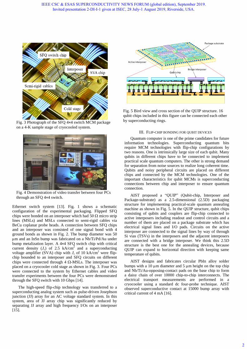
chips were connected through 4 -MSLs. The interposer wasplaced on a cryocooler cold stage as shown in Fig. 3. Four PCswere connected to the system by Ethernet cables and videotransfer experiments between the four PCs were demonstratedthrough the SFQ switch with 10 Gbps [14].
The high-speed flip-chip technology was transferred to a superconducting analog system such as pulse-driven Josephson junction (JJ) array for an AC voltage standard system. In this system, area of JJ array chip was significantly reduced by separating JJ array and high frequency I/Os on an interposer [15].
III. FLIP-CHIP BONDING FOR QUBIT DEVICES
Quantum computer is one of the prime candidates for future information technologies. Superconducting quantum bits require MCM technologies with flip-chip configurations by two reasons. One is intrinsically large size of each qubit. Many qubits in different chips have to be connected to implement practical scale quantum computers. The other is strong demand for separation from noise sources to realize long coherent time. Qubits and noisy peripheral circuits are placed on different chips and connected by the MCM technologies. One of the important characteristics for qubit MCMs is superconducting connections between chip and interposer to ensure quantum connection.
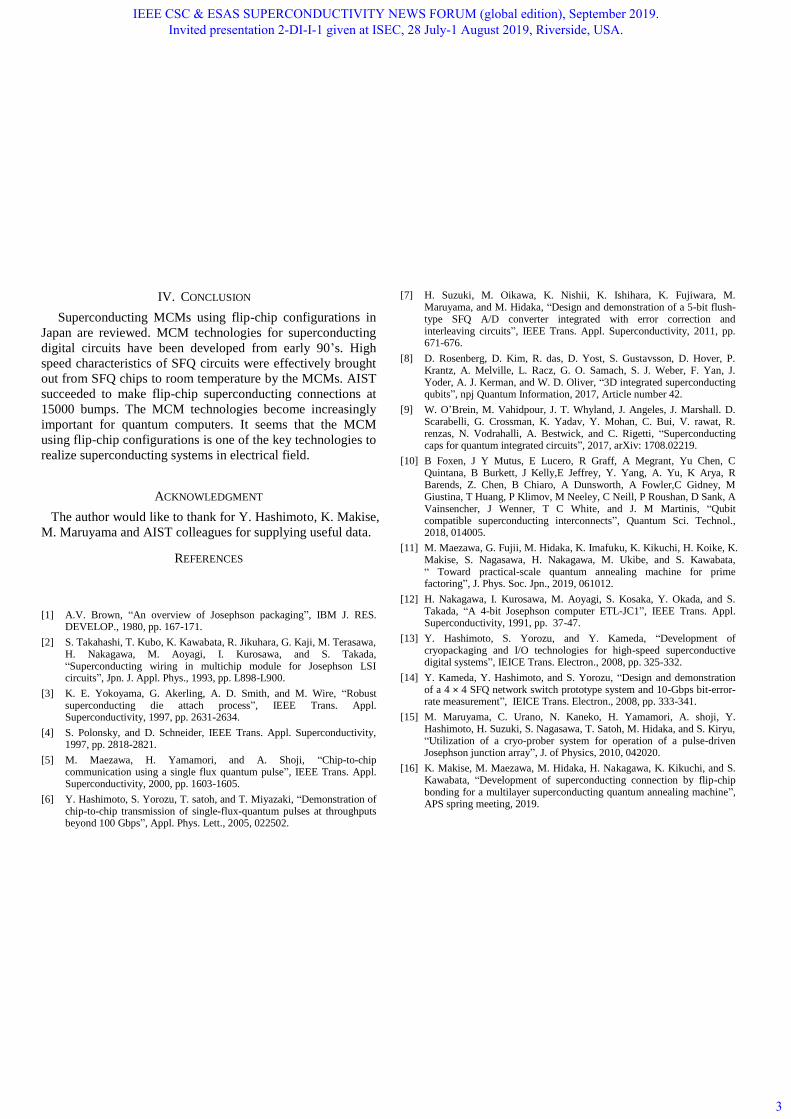
AIST proposed a “QUIP” (Qubit-chip, Interposer and Package-substrate) as a 2.5-dimensional (2.5D) packaging structure for implementing practical-scale quantum annealing machine as shown in Fig. 5. In the QUIP structure, qubit chips consisting of qubits and couplers are flip-chip connected to active interposers including readout and control circuits and a number of them are placed on a package substrate which has electrical signal lines and I/O pads. Circuits on the active interposer are connected to the signal lines by way of through Si vias (TSVs) in the interposers and the adjacent interposers are connected with a bridge interposer. We think this 2.5D structure is the best one for the annealing devices, because QUIP can expand to horizontal direction with keeping same temperature of qubits.
AIST designs and fabricates circular PbIn alloy solder
bumps with a 10 m diameter and 5 m height on the top chip and Nb/Ti/Au-opposing-contact pads on the base chip to form a daisy chain of over 10000 chip-to-chip interconnects. The electrical transport measurements are performed in a cryocooler using a standard dc four-probe technique. AIST observed superconductive contact at 15000 bump array with critical current of 4 mA [16].
Fig. 3 Photograph of the SFQ 4×4 switch MCM package
on a 4-K sample stage of cryocooled system.
Fig. 4 Demonstration of video transfer between four PCs
through an SFQ 4×4 switch.
Fig. 5 Bird view and cross section of the QUIP structure. 16
qubit chips included in this figure can be connected each other
by superconducting rings.
IEEE CSC & ESAS SUPERCONDUCTIVITY NEWS FORUM (global edition), September 2019. Invited presentation 2-DI-I-1 given at ISEC, 28 July-1 August 2019, Riverside, USA.
2
IV. CONCLUSION
Superconducting MCMs using flip-chip configurations in
Japan are reviewed. MCM technologies for superconducting
digital circuits have been developed from early 90’s. High
speed characteristics of SFQ circuits were effectively brought
out from SFQ chips to room temperature by the MCMs. AIST
succeeded to make flip-chip superconducting connections at
15000 bumps. The MCM technologies become increasingly
important for quantum computers. It seems that the MCM
using flip-chip configurations is one of the key technologies to
realize superconducting systems in electrical field.
ACKNOWLEDGMENT
The author would like to thank for Y. Hashimoto, K. Makise,
M. Maruyama and AIST colleagues for supplying useful data.
REFERENCES
[1] A.V. Brown, “An overview of Josephson packaging”, IBM J. RES. DEVELOP., 1980, pp. 167-171.
[2] S. Takahashi, T. Kubo, K. Kawabata, R. Jikuhara, G. Kaji, M. Terasawa,H. Nakagawa, M. Aoyagi, I. Kurosawa, and S. Takada, “Superconducting wiring in multichip module for Josephson LSI circuits”, Jpn. J. Appl. Phys., 1993, pp. L898-L900.
[3] K. E. Yokoyama, G. Akerling, A. D. Smith, and M. Wire, “Robust superconducting die attach process”, IEEE Trans. Appl. Superconductivity, 1997, pp. 2631-2634.
[4] S. Polonsky, and D. Schneider, IEEE Trans. Appl. Superconductivity,1997, pp. 2818-2821.
[5] M. Maezawa, H. Yamamori, and A. Shoji, “Chip-to-chip communication using a single flux quantum pulse”, IEEE Trans. Appl. Superconductivity, 2000, pp. 1603-1605.
[6] Y. Hashimoto, S. Yorozu, T. satoh, and T. Miyazaki, “Demonstration of chip-to-chip transmission of single-flux-quantum pulses at throughputs beyond 100 Gbps”, Appl. Phys. Lett., 2005, 022502.
[7] H. Suzuki, M. Oikawa, K. Nishii, K. Ishihara, K. Fujiwara, M. Maruyama, and M. Hidaka, “Design and demonstration of a 5-bit flush-type SFQ A/D converter integrated with error correction and interleaving circuits”, IEEE Trans. Appl. Superconductivity, 2011, pp. 671-676.
[8] D. Rosenberg, D. Kim, R. das, D. Yost, S. Gustavsson, D. Hover, P.Krantz, A. Melville, L. Racz, G. O. Samach, S. J. Weber, F. Yan, J. Yoder, A. J. Kerman, and W. D. Oliver, “3D integrated superconducting qubits”, npj Quantum Information, 2017, Article number 42.
[9] W. O’Brein, M. Vahidpour, J. T. Whyland, J. Angeles, J. Marshall. D. Scarabelli, G. Crossman, K. Yadav, Y. Mohan, C. Bui, V. rawat, R. renzas, N. Vodrahalli, A. Bestwick, and C. Rigetti, “Superconducting caps for quantum integrated circuits”, 2017, arXiv: 1708.02219.
[10] B Foxen, J Y Mutus, E Lucero, R Graff, A Megrant, Yu Chen, C Quintana, B Burkett, J Kelly,E Jeffrey, Y. Yang, A. Yu, K Arya, R Barends, Z. Chen, B Chiaro, A Dunsworth, A Fowler,C Gidney, M Giustina, T Huang, P Klimov, M Neeley, C Neill, P Roushan, D Sank, A Vainsencher, J Wenner, T C White, and J. M Martinis, “Qubit compatible superconducting interconnects”, Quantum Sci. Technol., 2018, 014005.
[11] M. Maezawa, G. Fujii, M. Hidaka, K. Imafuku, K. Kikuchi, H. Koike, K.Makise, S. Nagasawa, H. Nakagawa, M. Ukibe, and S. Kawabata, “ Toward practical-scale quantum annealing machine for prime factoring”, J. Phys. Soc. Jpn., 2019, 061012.
[12] H. Nakagawa, I. Kurosawa, M. Aoyagi, S. Kosaka, Y. Okada, and S. Takada, “A 4-bit Josephson computer ETL-JC1”, IEEE Trans. Appl. Superconductivity, 1991, pp. 37-47.
[13] Y. Hashimoto, S. Yorozu, and Y. Kameda, “Development of cryopackaging and I/O technologies for high-speed superconductive digital systems”, IEICE Trans. Electron., 2008, pp. 325-332.
[14] Y. Kameda, Y. Hashimoto, and S. Yorozu, “Design and demonstration of a 4 × 4 SFQ network switch prototype system and 10-Gbps bit-error-rate measurement”, IEICE Trans. Electron., 2008, pp. 333-341.
[15] M. Maruyama, C. Urano, N. Kaneko, H. Yamamori, A. shoji, Y. Hashimoto, H. Suzuki, S. Nagasawa, T. Satoh, M. Hidaka, and S. Kiryu,“Utilization of a cryo-prober system for operation of a pulse-drivenJosephson junction array”, J. of Physics, 2010, 042020.
[16] K. Makise, M. Maezawa, M. Hidaka, H. Nakagawa, K. Kikuchi, and S. Kawabata, “Development of superconducting connection by flip-chip bonding for a multilayer superconducting quantum annealing machine”, APS spring meeting, 2019.
IEEE CSC & ESAS SUPERCONDUCTIVITY NEWS FORUM (global edition), September 2019. Invited presentation 2-DI-I-1 given at ISEC, 28 July-1 August 2019, Riverside, USA.
3