Embed Size (px)
Citation preview

Enclosure: ENSC 340 Hockey JACK Functional Specifications
JACKD Inc.Simon Fraser University
Burnaby, BCV5H 1S6
November 5th, 2001
Dr. Andrew RawiczSchool of Engineering ScienceSimon Fraser UniversityV5A 1S6
RE: ENSC 340 Design Specification for Automated Air Hockey Player
Dear Dr. Rawicz,
The attached document, Hockey JACK Design Specification, outlines the design specificationsfor our automated air hockey player system. The goal of our project is to design and build anautonomous air hockey player. It will include a sensor system to locate a puck, anelectromechanical device to hit the puck, and an intelligent algorithm for strategic play.
This document lists the designs of the overall system and the specifications of the various blocksof the system. The fundamental blocks include a puck-sensing apparatus, a processing-unit, anarm actuator, and an arm sensor feedback mechanism.
Should you have any questions or concerns regarding our functional specification, please contactus via email, [email protected].
Sincerely,
Judy Cha, VP External

Submitted by: JACKD Inc.Dave Boen, Judy Cha,Alex Kwan, Kevin Yoon,Clarence Wong
Head Contact:
Group Contact:
Dave BoenSchool of [email protected]@sfu.ca
Submitted To: Andrew RawiczSchool of EngineeringScienceSimon Fraser University
Steve WhitmoreSchool of EngineeringScienceSimon Fraser University
Date: November 5th, 2001
Design Specifications for a TM
Interactive Air Hockey System

Property of JACKD Inc, ©2001 Page ii
Abstract
JACKD Inc. is currently endeavoring to build the HockeyJACK air hockey unit. This low-cost,automated-opponent is devised of three major subsystems: a puck-sensing array, a processingunit to map the trajectory of the puck, and an actuator system to move the mallet to intercept thepuck. The sensor array utilizes two lines of 20 reflective sensors that continuously scan forchanges in the input light intensity interpreting inputs that break a threshold voltage as a detectedpuck. These sensors are time-division-multiplexed to the processing unit, which thenextrapolates the trajectory of the puck using in-house developed algorithm. From this data, thetarget position of the mallet can be determined and an appropriate signal can be sent to the motorto actuate the mallet. The motor is placed behind the rink moving an arm that translates theangular position of the shaft to the lateral position of the mallet along the rack.

Property of JACKD Inc, ©2001 Page iii
Design Specification
Table of Contents
Abstract ..........................................................................................................................................ii
Table of Contents .........................................................................................................................iii
List of Figures ................................................................................................................................ v
List of Tables ................................................................................................................................vi
Glossary........................................................................................................................................vii
1 Introduction ........................................................................................................................... 1
2 System Overview ................................................................................................................... 2
3 Table Sensing Sub-System.................................................................................................... 3
3.1 Sensor Layout...................................................................................................................... 33.2 Determination of Puck's Position........................................................................................ 53.3 Sensor System Design.......................................................................................................... 6
3.3.1 Power Supply for Sensor System................................................................................ 63.3.2 Sensors ........................................................................................................................ 7
3.4 Sensor Output: Analog to Digital Conversion Scheme....................................................... 83.4.1 Reference Signal ......................................................................................................... 83.4.2 Comparator.................................................................................................................. 93.4.3 Buffer ........................................................................................................................ 113.4.4 Rectifier..................................................................................................................... 11
3.5 Time Multiplexing Sensor Signals..................................................................................... 12
4 Processing Unit Sub-System............................................................................................... 15
4.1 Hardware Selection........................................................................................................... 154.1.1 Parallel Port Interfacing ............................................................................................ 164.1.2 CPLD Interface ......................................................................................................... 184.1.3 Interface Board External Interfacing......................................................................... 184.1.4 Verilog Substructure ................................................................................................. 18
4.2 Software Interface ............................................................................................................. 20
5 Arm Actuation and Arm Sensors ...................................................................................... 21
Property of JACKD Inc, ©2001 Page iv
Design Specification
5.1 Motor Selection ................................................................................................................. 215.1.1 DC Motor .................................................................................................................. 215.1.2 RC Servo Motor ........................................................................................................ 22
5.2 Mechanical Setup .............................................................................................................. 225.2.1 Rack........................................................................................................................... 235.2.2 Arm............................................................................................................................ 245.2.3 Mallet Holder ............................................................................................................ 255.2.4 Mounting Apparatus.................................................................................................. 26
5.3 Arm Sensors....................................................................................................................... 27
6 Control Algorithm............................................................................................................... 29
7 Testing .................................................................................................................................. 30
7.1 Table Sensors .................................................................................................................... 307.1.1 Reference Level Calibration...................................................................................... 307.1.2 Sensors Operation ..................................................................................................... 30
7.2 Control Algorithm ............................................................................................................. 307.2.1 Directed Straight Line Detection............................................................................... 307.2.2 Directed Straight Line Detection (Angled) ............................................................... 307.2.3 Directed Reflected Angle Detection ......................................................................... 30
7.3 Processing Unit ................................................................................................................. 317.3.1 Visual Inspection and Power Tests ........................................................................... 317.3.2 Manual Arm Control ................................................................................................. 317.3.3 PC Connectivity Test ................................................................................................ 31
7.4 RAMA System .................................................................................................................... 317.4.1 Motor Operation Test ................................................................................................ 317.4.2 Motor Precision Test ................................................................................................. 317.4.3 System Integrity Test ................................................................................................ 32
8 Appendix .............................................................................................................................. 33
8.1 Parts List ........................................................................................................................... 338.2 Schematics......................................................................................................................... 34
8.2.1 Table Sensor Schematic ............................................................................................ 348.2.2 Processing Unit Schematic........................................................................................ 35

Property of JACKD Inc, ©2001 Page v
Design Specification
List of Figures
Figure 1: System Block Overview 2Figure 2: HockeyJACK Table Dimensions 2Figure 3: Table Sensing Sub-System Context Diagram 3Figure 4: Layout of the Sensors(Top View) 4Figure 5: Sensor Mount on the Table 5Figure 6: Illustration of Sensors Arrangement (Portion) 5Figure 7: Case 1 - Three Sensors On 6Figure 8: Case 2 - Four Sensors On 6Figure 9: Three-terminal adjustable voltage regulator, LM 317 6Figure 10: The Schematic of LM317 to Generate Voltage Supply 7Figure 11: The Schematic of QRB1113/1114 7Figure 12: The Designed Schematic of the Sensor for Puck Detection 8Figure 13: A Voltage Divider for Reference Signal 9Figure 14 : Schematic Diagram for the Comparator 10Figure 15 : Normal State of the Comparator Output 10Figure 16 : Output of Sensor and Comparator with Puck Present 11Figure 17 : Schematic Diagram of the Rectifier 12Figure 18 : Output of the Rectifier 12Figure 19: Sensor Outputs Connection to Data Selectors 14Figure 20: Processing Unit Sub-System Context Diagram 15Figure 21: Processing Unit Functional Diagram 16Figure 22: D-Sub 25 Parallel Port Connector 17Figure 23: CPLD Verilog File Hierarchy 19Figure 24: Sensor Read Cycle 19Figure 25: Command Write Cycle 19Figure 26: Command Set Definition 20Figure 27: Arm Actuator Unit Sub-System Context Diagram 21Figure 28 - H-bridge block diagram for DC motor control 21Figure 29: Top View of Mechanical Setup 23Figure 30: Simplified Isometric View of KrisTrack Rail 24Figure 31: Side View of Modified KrisTrack Sliding Unit 24Figure 32 - Cross-sectional view of KrisTrack Rail 24Figure 33: Top View of Arm 25Figure 34: Simplified Diagram of Mallet Holder 26Figure 35 - Mounting Apparatus 27Figure 36: Control Algorithm Flow Chart 29Figure 37 : The Sensor Schematic Diagram 34Figure 38 : Analog to Digital Conversion Schematic Diagram 34

Property of JACKD Inc, ©2001 Page vi
Design Specification
List of Tables
Table 1: Parametric Table for LM339 9Table 2 : Parametric Table for LM324 11Table 3: Important Parameter Values for the MC14512B 8-Channel Data Selector 13Table 4: Truth Table for MC14512B 13Table 5: Parallel Port - CPLD Interface Pinout 17Table 6- Hitec HS-805BB RC Servo Specifications 22Table 7: Specification for Accuride Model 2009-14 25

Property of JACKD Inc, ©2001 Page vii
Design Specification
GlossaryTerm DefinitionMallet The striker piece that is used by the player to strike the puck.Rink The arena surface in which the game is played.Goal The horizontal slots on either side of the rink.Centerline The line the runs along the center of the rink. Parallel to short-side of rink.
CPLD Complex Programmable Logic Device. A fast, configurable logic devicecontaining flip-flops and combinatorial logic.
PWM Pulse Width Modulation. A technique enabling control of servo motors, byvarying the duty cycle and pulse width of a signal.
Rack The device laid across the short side of the rink to guide the HockeyJACKsmallet.
Arm The device that extends from a servo motor located behind the rink to the rackin order to control the lateral position of the mallet.
RAMA or Rack-Arm-Motor ApparatusTM, consists of the 3 components that make upthe mallet controller mechanism.

Property of JACKD Inc, ©2001 Page 1
Design Specification
1 Introduction
What happens when a human player simply cannot find another human opponent to play? TheHockeyJACK brings the comfort and excitement of automated play to the average air hockeyenthusiast.
Many air hockey players practice on tables with blocked off goals, so that pucks entering a goalsimply bounce off and return to the player. This method lacks excitement and force, and is oflittle value to the player without the calculated response of a live player that is the nature of thefast-paced air hockey game. Our project attempts to address the challenge of developinginteractive, physical play with a human air hockey opponent. The HockeyJACK design is a low-cost system that will enable hobbyists to construct their own opponents. At this phase of ourproject, HockeyJACK is not intended to be a self-contained unit for general public use. Therewill be open circuit boards and exposed electrical components, as our primary goal does notinclude fine attention to the aesthetics of the system.
The purpose of this document is to describe the design requirements of the HockeyJACKsystems and the deliverables of JACKD Inc. to its customers. This document is directedtowards our project supervisors, Dr. Andrew Rawicz and Mr. Steve Whitmore, the design staff ofJACKD Inc, and external consultants and financiers.
Property of JACKD Inc, ©2001 Page 2
Design Specification
2 System Overview
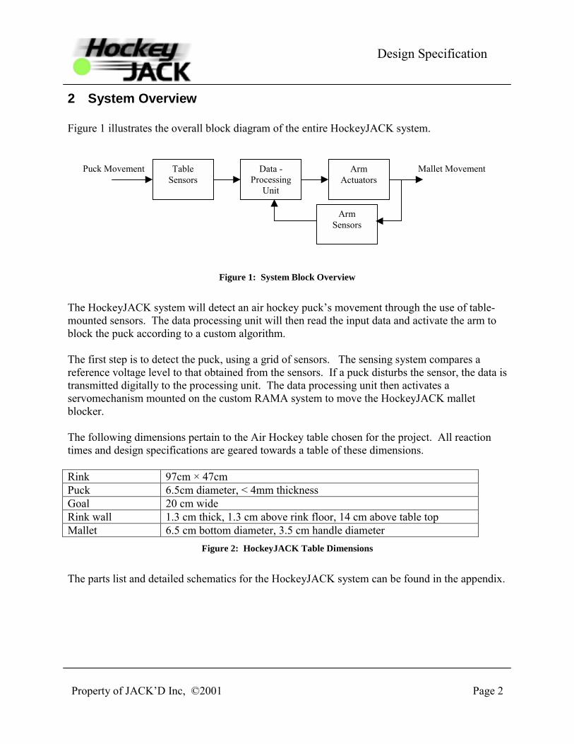
Figure 1 illustrates the overall block diagram of the entire HockeyJACK system.
Figure 1: System Block Overview
The HockeyJACK system will detect an air hockey pucks movement through the use of table-mounted sensors. The data processing unit will then read the input data and activate the arm toblock the puck according to a custom algorithm.
The first step is to detect the puck, using a grid of sensors. The sensing system compares areference voltage level to that obtained from the sensors. If a puck disturbs the sensor, the data istransmitted digitally to the processing unit. The data processing unit then activates aservomechanism mounted on the custom RAMA system to move the HockeyJACK malletblocker.
The following dimensions pertain to the Air Hockey table chosen for the project. All reactiontimes and design specifications are geared towards a table of these dimensions.
Rink 97cm × 47cmPuck 6.5cm diameter, < 4mm thicknessGoal 20 cm wideRink wall 1.3 cm thick, 1.3 cm above rink floor, 14 cm above table topMallet 6.5 cm bottom diameter, 3.5 cm handle diameter
Figure 2: HockeyJACK Table Dimensions
The parts list and detailed schematics for the HockeyJACK system can be found in the appendix.
TableSensors
Data -Processing
Unit
ArmActuators
Mallet MovementPuck Movement
ArmSensors

Property of JACKD Inc, ©2001 Page 3
Design Specification
3 Table Sensing Sub-System
The Table Sensing Sub-System detects the pucks movement and passes this information to thedata processing unit. Figure 3 illustrates the context diagram for this system.
Figure 3: Table Sensing Sub-System Context Diagram
3.1 Sensor LayoutTo accurately determine the trajectory of the puck, one position vector is all the informationrequired. Once the position vector of the puck is known, then the trajectory line can be easilydeduced from it. Since the position vector requires a starting point and end point, two rows ofsensors are implemented. To accommodate for bounce off of the rink walls, we can use the Lawof Reflection, which states that the angle of incidence equals the angle of reflection. Theposition vector obtained contains the information on the angle of the incidence. The angle of thereflection is then used to generate the second position vector. In summary, two rows of sensorsare enough to obtain the essential information of the trajectory of the puck.
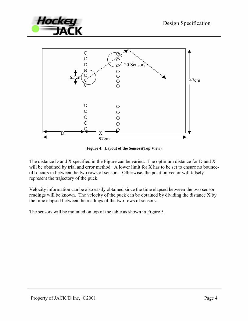
In addition, a fine grid system is needed to locate where the puck is along the row. To be able tolocate the puck accurately, three or four adjacent sensors are needed to cover its area. Becausethe width of the table is 47cm and the diameter of the puck is 6.5cm, a simple calculation resultsin twenty sensors per row. Figure 4 shows the top view of the sensor system layout.
TableSensors
Data -Processing
Unit
ArmActuators
Mallet MovementPuck Movement
ArmSensors
Property of JACKD Inc, ©2001 Page 4
Design Specification
Figure 4: Layout of the Sensors(Top View)
The distance D and X specified in the Figure can be varied. The optimum distance for D and Xwill be obtained by trial and error method. A lower limit for X has to be set to ensure no bounce-off occurs in between the two rows of sensors. Otherwise, the position vector will falselyrepresent the trajectory of the puck.
Velocity information can be also easily obtained since the time elapsed between the two sensorreadings will be known. The velocity of the puck can be obtained by dividing the distance X bythe time elapsed between the readings of the two rows of sensors.
The sensors will be mounted on top of the table as shown in Figure 5.
XD
20 Sensors
47cm
97cm
6.5cm

Property of JACKD Inc, ©2001 Page 5
Design Specification
Figure 5: Sensor Mount on the Table
The distance between the table surface and the sensor mount will be less than 2cm so that notmuch ambient light disturbs the system. Also the mount will have a protection wall to protectthe sensors from potential puck impact.
3.2 Determination of Puck's PositionReflective object sensors are arranged in a row to determine the presence and the position of apuck. Sensor arrangement is critical to accurately determine the center of the puck for trajectoryprediction. To locate the puck's center requires the sensors to be separated by less than thediameter of the puck. Calculation of the puck's center is achieved by separating sensors by 2cmin a row. Figure 6 shows a portion of the sensors arrangement.
2cm 2cm 2cm 2cm
Figure 6: Illustration of Sensors Arrangement (Portion)
Two cases will be encountered as a puck passes through this row of sensors: three sensors turnedon, or four sensors turned on. These two cases are shown pictorially in Figure 7 and Figure 8.

Property of JACKD Inc, ©2001 Page 6
Design Specification
Puck(6.5cm diameter)
Figure 7: Case 1 - Three Sensors On
Puck(6.5cm diameter)
Figure 8: Case 2 - Four Sensors On
Case 1: The puck's center is determined to be the location of the middle sensor. Althoughthe puck might be displaced slightly on one side, the worse case scenario gives anerror of ±0.5cm (<8%) from the middle sensor's location. This error is tolerablesince the mallet is wide enough to ensure contact with the puck.
Case 2: The puck's center is determined to be half the displacement between the outer twoactive sensors. In worst case scenario, this case gives an error of ±0.25cm (<4%)from the calculated middle point of the outer two sensors.
3.3 Sensor System Design
3.3.1 Power Supply for Sensor SystemThree-terminal adjustable voltage regulators, LM317 will be used to supply appropriate voltagelevels for electronic components used in the sensor system. The LM317 is capable of supplyingin excess of 1.5A over a 1.2V to 32V voltage range. It guarantees one percent of the outputvoltage tolerances and its operating temperature is from 0°C to 125°C. Figure 9 shows thepackage of the regulator.
Figure 9: Three-terminal adjustable voltage regulator, LM 317
The LM317 will be used to supply 1V to a LED and 5V to a BJT transistor component. Inaddition, it will be used to supply 5V to a comparator as well as a buffer in the sensor system.Figure 10 shows how it will be configured to generate desired voltage outputs.

Property of JACKD Inc, ©2001 Page 7
Design Specification
Figure 10: The Schematic of LM317 to Generate Voltage Supply
Although not shown in Figure 10, 0.1µF ~ 1µF bypass input and output capacitors to ground willbe added to reject the rippling effects of the power supply.
The output voltage will be regulated as follows:
21
21 RIRRVV ADJREFout +
+=
Since the resistor R2 is a potentiometer, a desired voltage level can be easily obtained in real-time.
3.3.2 SensorsThe layout of sensors guarantees accurate data capture to determine the trajectory of the puckthus predicting its final destination. In this section, sensor operation will be explained in details.
The QRB1113/1114 IR sensors will be used for our puck detecting system. Figure 11 shows theschematic of the QRB1113 from its design specification.
Figure 11: The Schematic of QRB1113/1114

Property of JACKD Inc, ©2001 Page 8
Design Specification
As shown in the above Figure, the QRB1113/1114 consists of an infrared emitting diode and aNPN silicon phototransistor. The phototransistor responds to radiation from the emitting diodeonly when a reflective object passes within its field of view so that the radiation gets reflectedback. Figure 12 shows the designed circuit of the sensor for the puck detection.
Figure 12: The Designed Schematic of the Sensor for Puck Detection
The LM317 voltage regulator will generate 5V and 1V voltage input for the transistor and theLED respectively. The two diodes in Figure 12, D1 and D2, protect the transistor and LEDs ofthe sensors from possible damages by excessive currents which might be due to possible circuitshorts. The capacitors, C1 and C2, provide a bypass for currents and eliminate noises comingfrom the power line.
The output signal, Vout will be generally high when there is no reflected radiation. When theradiation generated by the diode gets reflected by the moving puck, the base of the transistorpicks up the radiation and draws a current. This current will lower the emitter current hence,pulling the Vout low. In other words, The output signal Vout will be an active low signal.
3.4 Sensor Output: Analog to Digital Conversion Scheme
The analog output signal from the sensor must be converted to a digital signal so that it iscompatible with the processing unit. For the analog to digital conversion, a comparator is chosensince a comparator can take two analog signals as its input and outputs either a high or lowdigital signal.
3.4.1 Reference SignalOne of the two inputs to the comparator is the sensor output signal and the other input is thereference signal that will be compared to the sensor output signal. This reference signal will be adc voltage that can be adjusted by using a variable resistor. The advantage of having a variableresistor is that a quick manual calibration of the reference signal can be easily done. Figure 13

Property of JACKD Inc, ©2001 Page 9
Design Specification
shows a simple voltage divider circuit with the variable resistor to calibrate the reference inputsignal.
Figure 13: A Voltage Divider for Reference Signal
3.4.2 Comparator
The reference signal and the sensor output signal can now be inputted to the comparator. TheLM339 (a Low Power, Low Offset Voltage, Quad Comparator) is chosen for the system. Thishas four comparators in a single chip. Table 1 summarizes important parameter values for theLM339.
Number of Channels 4Response Time, typ (us) .50Supply Voltage, min (Volt) 3Supply Voltage, max (Volt) 36Supply Current per Channel, typ (mA) .20Input Range Vcm to V-Output Type Open DrainOutput Current, typ (mA) 16Vos, Room max (mV) 2,5Input Bias Current, max (nA) 400
Table 1: Parametric Table for LM339
The LM317 voltage regulator again will generate the supply voltage for the comparator. Figure14 shows the schematic diagram of the comparator including the voltage divider circuit for thereference signal.

Property of JACKD Inc, ©2001 Page 10
Design Specification
Figure 14 : Schematic Diagram for the Comparator
Since the sensor output signal is active low, the sensor output signal is normally high. Hence, thereference signal is a dc voltage signal whose voltage level is right below the lowest point of theoutput signal of the sensor. The output of the comparator then is normally a negative powersupply. Figure 15 describes the normal state of the sensor without the presence of the puck.
Figure 15 : Normal State of the Comparator Output
When the sensor detects the puck, the output signal is lowered past the reference signal. Then,the output of the comparator toggles between the positive power supply, when the output signalof the sensor is lower than the reference signal, and the negative power supply, when the outputsignal of the sensor is higher than the reference signal. The output signal of the sensor with thepresence of the puck is described in Figure 16.
Reference
Sensor Output
Comparator Output

Property of JACKD Inc, ©2001 Page 11
Design Specification
Figure 16 : Output of Sensor and Comparator with Puck Present
3.4.3 BufferSince more circuitry is connected to the output of the comparator, a buffer is used to isolate theoutput signal of the comparator. The output of the comparator then is not affected by thefollowing stages of circuitry. The LM324, the Low Power Quad Operational Amplifier is usedin a unity gain inverting amplifier configuration to be used as a buffer. Table 2 summarizesimportant parameter values for the LM324.
Channels (Channels) 4Input Output Type Vcm to V-,Not R-R OutBandwidth, typ (MHz) 1Slew Rate, typ (Volts/usec) .50Supply Current per Channel, typ (mA) .18Minimum Supply Voltage (Volt) 3Maximum Supply Voltage (Volt) 32Offset Voltage, Max (mV) 3,7Input Bias Current, Temp Max (nA) 200,500Output Current, typ (mA) 20Voltage Noise, typ (nV/Hz) 40Shut down No
Table 2 : Parametric Table for LM324
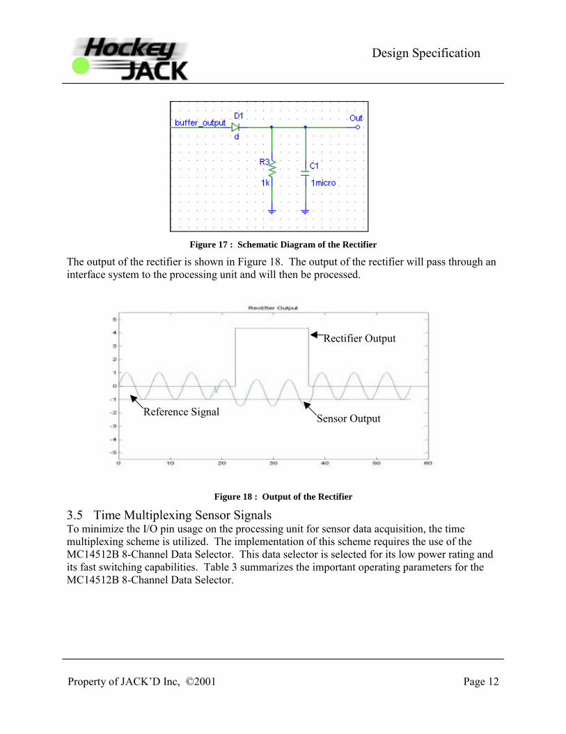
3.4.4 Rectifier
A rectifier will be used to maintain a dc high-level output in the presence of the puck. Thecircuit design is shown in the Figure 17.
Reference
Sensor Output
Comparator Output
Property of JACKD Inc, ©2001 Page 12
Design Specification
Figure 17 : Schematic Diagram of the Rectifier
The output of the rectifier is shown in Figure 18. The output of the rectifier will pass through aninterface system to the processing unit and will then be processed.
Figure 18 : Output of the Rectifier
3.5 Time Multiplexing Sensor SignalsTo minimize the I/O pin usage on the processing unit for sensor data acquisition, the timemultiplexing scheme is utilized. The implementation of this scheme requires the use of theMC14512B 8-Channel Data Selector. This data selector is selected for its low power rating andits fast switching capabilities. Table 3 summarizes the important operating parameters for theMC14512B 8-Channel Data Selector.
Sensor Output
Rectifier Output
Reference Signal

Property of JACKD Inc, ©2001 Page 13
Design Specification
Symbol Parameter Value Unit
VDDDC Supply Voltage
Range -0.5 to +18.0 V
Vin, VoutInput or OutputVoltage Range -0.5 to VDD+0.5 V
Iin, IoutInput or Output
Current ±10 MA
PD Power Dissipation 500 MW
tTLH, tTHLOutput Rise and Fall
Time Typ. 100 Ns
Table 3: Important Parameter Values for the MC14512B 8-Channel Data Selector
Sensors are divided into groups of eight, and the sensor outputs from each group are connectedto the eight channels on the MC14512B. The processing unit then switches the select signals (A,B, and C) for the data selector with respect to the system clock. The relationship between theselect signals and data selector output is described in the truth table in Table 4. The eight inputsof this data selector is represented by X0, X1, X2, , X7.
Select C Select B Select A Inhibit Disable Output Y0 0 0 0 0 X00 0 1 0 0 X10 1 0 0 0 X20 1 1 0 0 X31 0 0 0 0 X41 0 1 0 0 X51 1 0 0 0 X61 1 1 0 0 X7X X X 1 0 0X X X X 1 High
ImpedenceTable 4: Truth Table for MC14512B
In doing so, the sensor outputs are time-multiplexed and are sampled at a rate of 1/8 of thesystem clock frequency (when all 8-channels on MC14512B are used). The minimumrequirement for the sensors sampling rate is 1kHz, and therefore the minimum system clockrequirement is 8kHz.
From Section 3.2, the puck simultaneously turns on multiple adjacent sensors. To maximize theefficiency and minimize the time lag of the data acquisition process, every fifth sensor output isconnected to the same data selector. This idea is illustrated in Figure 19 with four data selectorbeing used.

Property of JACKD Inc, ©2001 Page 14
Design Specification
DataSelector 1
DataSelector 2
to DS 3
to DS 4 to DS 4
to DS 3 to DS 3
to DS 4
Figure 19: Sensor Outputs Connection to Data Selectors
Using the scheme depicted in Figure 19, the processing unit will poll all data selector outputscontinuously. Since only 5 channels of the MC14512B are used, the sensor outputs are sampledat a rate of 1/5 of the system clock. The minimum requirement for the sensors sampling rate is1kHz, and therefore the minimum system clock requirement is 5kHz.

Property of JACKD Inc, ©2001 Page 15
Design Specification
4 Processing Unit Sub-System
The processing unit takes information gathered by the table sensing sub-system andformulates the decision to move the mallet arm. Figure 20 illustrates the role of this sub-system in the overall hierarchy.
Figure 20: Processing Unit Sub-System Context Diagram
4.1 Hardware Selection
A number of 8 and 16 bit microprocessors were considered for use in the HockeyJACKprocessing system. Among those were the
• Microchip PIC• Atmel Mega103• Motorola HC11 and HC12
However, the PIC and HC chips lack the ability to handle large amounts of memory andprogramming the Mega103 requires additional hardware.
The PC was chosen as a controller unit for the following reasons:• Widespread availability of inexpensive parts and software• Scalability in processing power• Easily programmed• Freely available real-time operating systems such as QNX• Familiarity with the system• Easily user interfaced through the use of keyboard and GUI displays
A primary disadvantage of the basic PC is a lack of I/O ports to interface external hardware. Thelargest data path is through the Parallel Port, which consists of a number of control signals andan 8-bit, bi-directional data bus. Therefore, additional hardware will be required to overcome theI/O limitation. An external CPLD will act as a combination multiplexer/PWM interface throughwhich the computer will interact with the table sensing and arm actuation subsystems.
The PC is also very bulky in its original form. However, an integrated PC with an on boardvideo chip was chosen to enable the computer to be uncased and hidden within the tablestructure.
TableSensors
Data -Processing
Unit
ArmActuators
Mallet MovementPuck Movement
ArmSensors

Property of JACKD Inc, ©2001 Page 16
Design Specification
4.1.1 Parallel Port InterfacingA number of choices are available to connect external devices to the PC. An ISA bus interfacewould enable the computer to interact with the system at high speeds, but was rejected due totime constraints.
Another option is a connection through the PCs parallel port. While slower in throughput(limited to around 200 KB/s), the parallel port will allow users to connect their own computers tothe sensor interface without the need of a dedicated computer. It will enable even non-technically savvy users to plug into the system and use it. For the purposes of this project, astripped down Pentium class computer will be embedded into the system.
Figure 21: Processing Unit Functional Diagram
A modern, bi-directional interface is obviously required, to exchange data and communications.This precludes the use of Standard (SPP) Parallel Port communications, which basically only hasoutput pins. Communications will utilize the Enhanced (EPP) Parallel Port communicationsstandard to exchange data. An EPP interface will require 16 pins on the CPLD device. Figure22 illustrates the type of connector used on the parallel port.
Sensor Input
Host Computer CPLD
Arm Output
ParallelPort
Commands
Sensor Data

Property of JACKD Inc, ©2001 Page 17
Design Specification
Figure 22: D-Sub 25 Parallel Port Connector
The D7-0 pins correspond to the bi-directional data bus, while S7-3 and C3-0 correspond tostatus register (IN) and control register (OUT) pins. The base address of the parallel port on thePC is 0x378. All data reads and writes will occur using this base address.
The EPP data register, uses additional control signals to ensure data is transferred properly. Thisregister is located at address base + 4 and can be read from or written to. Table 5 describes themodified EPP and control signals from the PC to the CPLD.
Pin Name Direction Purpose1 Nstrobe Out A low on this line indicates a
Write, High indicates a Read2-9 D 0-7 In-Out Data Bus. Bi-directional10 Nack In Interrupt Line. Interrupt occurs
on Positive (Rising) Edge.11 Nwait In Used for handshaking. An EPP
cycle can be started when low,and finished when high.
12 Tsensor In Indicates incoming Table SensorData
13 Asensor In Indicates incoming Arm SensorData
14 NdataStrobe Out When Low, indicates Datatransfer
15 Error / Fault In Spare16 Reset Out Reset - Active Low17 Ncommand Out When low, indicates PC
Command sent18-25 Ground GND Ground
Table 5: Parallel Port - CPLD Interface Pinout

Property of JACKD Inc, ©2001 Page 18
Design Specification
4.1.2 CPLD InterfaceAn Altera CPLD, the EPM7128SLC84-6, operates as the main link between the PC, sensing andarm subsystems. Since it is electrically programmable, the CPLD retains its program in theabsence of power, without additional circuitry. The 7128SLC84-6 is packaged in an 84-pinPlastic Lead Chip Carrier (PLCC) format, containing 60 general-purpose I/O pins. With thesensing system I/O pin requirements at 11 pins and 1 PWM control pin to service the servo,additional pins can be devoted to pushbuttons and LEDs for manual user control and debuggingpurposes.
Eleven I/O pins dedicated to the sensor system provide an 8-bit input path into the CPLD and 3multiplexor control pins (A, B, C) to control sensor data reads.
The CPLD also contains 128 flip-flops, which will be utilized in counters and FIFO bufferingapplications.
A 1 MHz clock controls the sampling rate and data communications. The sensing systemrequires a sustained sampling rate of at least 1 KHz, necessitating an actual read rate of 8 KHz,due to the forty sensors being read byte-wise at a time, five times in succession. Ideally, theCPLD would capture sensor data at a much higher rate, as close to instantaneously as possible.The use of this higher clock rate will also allow the CPLD to clear the Parallel Port of datatransfers as quickly as possible to allow the computer to send commands.
4.1.3 Interface Board External InterfacingThe Interface Board contains,
• Two 26-pin shrouded header, with 13 usable pins, to allow communications between theCPLD, sensor and arm subsystems.
• Two pushbuttons (Omron type B3F switch type) to allow manual user control without thecomputer present.
4.1.4 Verilog Substructure
The following subsystems in Figure 23 will be implemented in the CPLD using the VerilogHardware Description Language.

Property of JACKD Inc, ©2001 Page 19
Design Specification
Figure 23: CPLD Verilog File Hierarchy
4.1.4.1 Parallel Port InterfaceThe Parallel Port Interface block decodes and encodes the EPP control signals to receivecommands and send data respectively. The Interface utilizes the EPP Data Read and Data Writecycles to receive commands and send data respectively on the combined Data/Command Bus.
Figure 24: Sensor Read Cycle Figure 25: Command Write Cycle
The command decoder will decode received commands and actuate a new command for thePWM motor interface or request a read from the sensor interface. The MSB of the commandwill indicate whether to initiate a sensor update or issue a PWM change.
Command (Binary) Description0XXX XXXX Initiate Sensor
Update
PC
Parallel PortInterface
SensorPolling
Interface
PWM MotorControl
CommandDecoder
User Pushbuttons
Sensors
Arm
Data (8 Bits)EPP
Control
Data/CommandBus (8Bits)
Command (8 Bits)
Sensor Data(8 Bits)
MuxControl (3
Bits)

Property of JACKD Inc, ©2001 Page 20
Design Specification
1000 0000 PWM Duty Cycle 01000 0001 PWM Duty Cycle 1
1110 0011 PWM Duty Cycle 99
Figure 26: Command Set Definition
The command decoder interprets inputs from the two onboard push-buttons, to allow arm left orarm right commands from the user for manual testing purposes.
4.1.4.2 Sensor InterfaceThe Sensor Interface responds to a PC request for a sensor update, a 0 in the MSB of thecommand byte, and initiates a burst sample of the forty sensors, eight at a time in successiveclock cycles. Forty of the CPLDs onboard flip-flops form a FIFO buffer necessary to capturethe five consecutive byte read cycles until sensor update request.
4.1.4.3 Servo Motor InterfaceThe servo motor interface reads the lower seven bits of the command byte upon detecting a 1 inthe MSB. Since the period of the PWM signal is 15 ms and the clock runs at a rate of 1 MHz, a14 bit counter is required to control the period. The motor interface interprets the 7 bit value asan offset value, to control duty cycle period in the range of 1-2 ms.
4.2 Software InterfacePC programming will be done using the QNX 6 Real Time Operating System (RTOS). Whilethe hardware requirements are higher to support the overhead of this operating system, relative toDOS, QNX offers a number of important features such as multi-process capability, interrupthandling and timers.
A C process will be developed (sensor_update) to automatically send the command to poll thesensors at regular intervals. The results of the sample will be placed in QNX shared memory andbe available to the control algorithm.

Property of JACKD Inc, ©2001 Page 21
Design Specification
5 Arm Actuation and Arm Sensors
Figure 27: Arm Actuator Unit Sub-System Context Diagram
5.1 Motor Selection
5.1.1 DC Motor
In an effort to minimize cost of the arm controller setup, the use of a simple DC motor wasexplored. Some experimentation was conducted with a geared-down Pittman 24V DC motor anda LMD18201 H-bridge by National Semiconductor in the setup shown in Figure 28.
Figure 28 - H-bridge block diagram for DC motor control
The DC motor was attached to the two outputs of the H-bridge. Three digital inputs (brake,direction, PWM) were also utilized. The function of the brake and direction inputs is obvious.The PWM signal defines the velocity of the shaft.
It was discovered that it was too difficult to achieve precision positioning of the motor withoutan attached inertial arm let alone with one. The torque of the motor also increased with velocity,which was not a desired dependency. While quick braking and reliable direction control weremuch desired features that the H-bridge provided, it was still difficult to map a given step inputlength to a certain angle of rotation, especially when an inertial and frictional torque is applied.Even if the optical encoder built into the Pittman motor was utilized, it would still be difficult todetermine how much voltage to apply in order to correct an offset position. The DC motor also
TableSensors
Data -Processing
Unit
ArmActuators
Mallet MovementPuck Movement
ArmSensors

Property of JACKD Inc, ©2001 Page 22
Design Specification
appeared to exhibit limits beyond which it did not behave according to the expectedcharacteristics.
A motor with more discrete settings or internal closed-loop control was required. A high-torqueRC servo would serve well for this application.
5.1.2 RC Servo Motor
The Hitec HS-805BB is one of the lower-priced, high-torque RC servos available. With a heavyduty nylon gear train it can put out some considerable force. Table 6 outlines the maincharacteristics of the motor.
Bearing TypeDual Ball Bearing
Operating Voltage 4.8V 6.0VTorque 19.8 kg/cm 24.7 kg/cmSpeed @ 60 degrees 0.19 s 0.15Size (L × W × H) 66 × 30 × 58 mm
Table 6- Hitec HS-805BB RC Servo Specifications
This servo has three inputs: a positive supply, a ground, and a pulse-width-modulated (PWM)control signal. The PWM signal is a square-wave of varying duty cycle which determines theangular position of the servo shaft. From the test plan described in Section 7.4, a 15ms signalwith a duty cycle varying between 1.2 and 2.1ms gives us a range of more than 90 degrees on theservo shaft. This range is more than the 60 degrees that is required, giving us a decent buffer forconfiguration. (Sixty degrees is an arbitrary range chosen on the basis that a wider angle wouldcall for more speed and torque on the motor while a smaller angle would require much greaterprecision from the motor.) Some fine-tuning may be done at later stages to find the frequencythat yields the highest angular resolution for our application.
This single-input control is much more advantageous over the DC motor setup since the torque isrelatively constant and no limits exist beyond which the motor behaves strangely, as the DCmotor did. Also because of the internal feedback of RC servos, little error is present in position.Precision can be increased by reducing the frequency of the input clock, albeit at the cost ofangular range.
5.2 Mechanical Setup
While the choice of the motor is crucial to the design of the RAMA system, the overallmechanical setup has to complement the decision. Our goal in design and assembly is threefold:simple, inexpensive, and low load for the motor. And the overall design can also be divided intofour parts, which are the motor, the rack, the arm, and the mallet holder. The next figure shows atop view of our final design.

Property of JACKD Inc, ©2001 Page 23
Design Specification
Figure 29: Top View of Mechanical Setup
Basically, the motor is the controlling centre. All motion of the RAMA system originates fromthis anchoring point. The motor provides angular motion of approximately 60 degrees. On topof the motor is where the arm is mounted. The arm is an extension of the spinning motor gear.The rack is a fixed piece upon which the arm slides on. The combination of arm and racktranslates the angular motion into lateral motion. Attached to the arm-rack hinge point is themallet holder. The mallet holder hangs from the rack on one end, and secures the mallet piece onthe other end.
When in operation, the data processing unit will send a signal to the motor. The motor willinterpret the signal and move to the commanded angular position. This will cause the arm toslide to a certain position on the rack. When the arm moves, the attached mallet holder will moveaccordingly. As a result, the RAMA system has the ability to intercept the incoming puck.
The description above is a brief introduction to the RAMA system. The following sections willprovide a more detailed discussion on the specific parts of this system.
5.2.1 RackThe rack is the piece of material on which the arm slides. In addition, the mallet holder hangsfrom the rack. Therefore, the rack must be stiff since it supports most of the weight of theRAMA system. Another major factor is friction. Since the arm moves on the rack, it mustprovide a sliding mechanism that minimizes the motor load.
Our choice is the lightweight KrisTrack pocket doorframe kit. The kit includes one rigid metalrail, and two wheeled sliders. They are shown in the following figures.
Rack
Motor
Mallet
ArmRink

Property of JACKD Inc, ©2001 Page 24
Design Specification
Figure 30: Simplified Isometric View ofKrisTrack Rail
Figure 31: Side View of Modified KrisTrackSliding Unit
While this domestic piece of equipment is not designed for our purpose, it satisfies many of ourselection criteria. Here are the dimensions of the KrisTrack pocket doorframe kit.
Figure 32 - Cross-sectional view of KrisTrack Rail
There are many advantages for using the KrisTrack kit. The rail is designed to be lightweight yetvery rigid. The sliding unit has two wheels on each side. As a result, movement is nearlyfrictional and very straight. The total of four wheels also permits a large amount of weight to besuspended over the sliding unit.
The sliding unit is modified for our design, mainly for the purpose of connection to the malletholder and the arm. This includes substituting the short spring-loaded screw in the original partsto the 10cm long steel screw. The head of the screw is attached to the mallet holder while thebody of the screw provides means for attachment to the arm.
5.2.2 ArmThe arm is the connection between the rotating motor and the sliding unit on the rack. For thispiece, many unique adjustments are needed on top of a normal rectangular metal piece. It mustbe lightweight to reduce the load on the motor. Its length must be able to vary for at least 10cmto accommodate for its swinging motion. Finally, it must have sufficient means to connect to themotor and the sliding unit.

Property of JACKD Inc, ©2001 Page 25
Design Specification
Our choice is a modified version of the Accuride Model 2009-14 Variable Height KeyboardSlide. The original application is for sliding computer keyboards and pencil drawers, but itsvariable sliding length adjustment fits well with our design. A simplified diagram is shownbelow,
Figure 33: Top View of Arm
Here are some of its specifications,
Length of Stationary Piece 35.56cm (14.00)Length of Slide Member 26.67cm (10.50)Maximum Load 34.09kg (75lb)Movement Steel ball bearings
Table 7: Specification for Accuride Model 2009-14
The Accuride slide is made of cold rolled steel and weights about 2lbs. However, its slidingmember utilizes carburized steel ball bearings, which provide smooth operation. This quality isvery advantageous since friction is assumed to attribute to most of the load on the motor.
Slight modifications will be needed to connect the arm piece to the motor and the sliding unit.This will involve drilling holes in the metal piece.
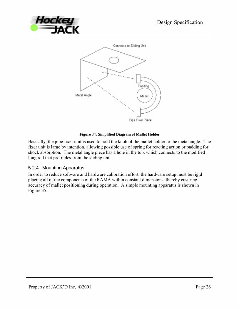
5.2.3 Mallet HolderThe mallet holder keeps the mallet in place, and moves according to the sliding unit of the rack.Our design consists of a metal angle and a plastic pipe fixer piece. The following figure showsthe arrangement,
Property of JACKD Inc, ©2001 Page 26
Design Specification
Figure 34: Simplified Diagram of Mallet Holder
Basically, the pipe fixer unit is used to hold the knob of the mallet holder to the metal angle. Thefixer unit is large by intention, allowing possible use of spring for reacting action or padding forshock absorption. The metal angle piece has a hole in the top, which connects to the modifiedlong rod that protrudes from the sliding unit.
5.2.4 Mounting ApparatusIn order to reduce software and hardware calibration effort, the hardware setup must be rigidplacing all of the components of the RAMA within constant dimensions, thereby ensuringaccuracy of mallet positioning during operation. A simple mounting apparatus is shown inFigure 35.

Property of JACKD Inc, ©2001 Page 27
Design Specification
Figure 35 - Mounting Apparatus
It will be constructed mainly of wood and functions to secure the servo in a fixed position withrespect to the rack. To increase tolerable puck speeds, we can set the entire apparatus back sothat the mallet has more time to move before the puck crosses the rack line. The rack will restabove the rink bottom by approximately 10cm giving some clearance space for the mallet-holding mechanism.
The servo will be placed at a distance of approximately 30cm to 40cm from the center of the rackset in the middle of the mounting apparatus. From this position we utilize 60 degrees of theservo rotational range to cover the 47cm of distance along the length of the rack. With a zero-load velocity of about 60 degrees/0.2 seconds, we can achieve fairly good reaction times, giventhat, theoretically, no opposing torque is present on the arm since the rack slider is frictionless.
5.3 Arm Sensors
Sensors will be used as a feedback mechanism for the RAMA system. The sensors used will bethe Fairchild QRB1113/1114 IR sensors, which is of the same type as the sensors used for puckdetection. Three sensors will be used to track the motion of the arm. Their schematics andoperation are very similar to the puck detection scheme.
Mallet MovementTableSensors
Data -Processing
Unit
ArmActuators
Puck Movement
ArmSensors

Property of JACKD Inc, ©2001 Page 28
Design Specification
Of the three sensors, one will be placed in the far-left end of the rack, to detect for the leftmostlimit position for the arm. One will be placed in the far-right end of the rack, to detect for therightmost limit position for the arm. When the arm is moving beneath either sensor, they areactivated, and the signal is sent as feedback to the processing unit. Knowing that the arm ismoving approaching the limiting position, the processing unit will halt all arm motion.
Another arm sensor will be placed in the centre on the rack. This sensor provides a safeguardmechanism for RC servo accuracy. After every motion, the arm is returned to its centralposition, as commanded by the control algorithm in the processing unit, which will be checkedand calibrated by this sensor.

Property of JACKD Inc, ©2001 Page 29
Design Specification
6 Control AlgorithmThe mission of the control algorithm is to intercept the puck from entering the goal. Theprocessing unit generates appropriate motor signals to react with any puck movements towardsthe goal. Figure 36 shows the high-level flow chart for the control algorithm.
Determine puck'sspeed andtrajectory
Signal Input
Puck movinginto goal area?
Calculate requiredmotor rotation
Generate PWMsignal to motor
Wait for puckinterception
Center mallet ongoal areaNo
Yes
Figure 36: Control Algorithm Flow Chart

Property of JACKD Inc, ©2001 Page 30
Design Specification
7 Testing7.1 Table Sensors
7.1.1 Reference Level Calibration1) After powering up the sensor units.2) On the sensor unit, adjust the reference level potentiometer to a level where the
"Calibration Required" LED just turns off.
NOTE: At the first use of equipment, please adjust the potentiometer such that the "CalibrationRequired" LED is turned on and then perform step 2.
7.1.2 Sensors Operation1) Calibrate the reference level as described in 7.1.1.2) Manually pass the puck under each sensor and observe the corresponding sensor test
LED. The sensor test LED should turn on as the puck is present under that sensor.
7.2 Control Algorithm
7.2.1 Directed Straight Line Detection1) Line up two test rails on the air hockey table so that the path is perpendicular to the short
side of the table.2) Place a puck between the two test rails and hit it towards the RAMA side.3) Observe if the corresponding sensor test LEDs turn on.4) Observe if the RAMA moves into the path to attempt a block.5) Observe if the central arm feedback sensor is turned on when the RAMA retracts.6) Repeat steps 1 to 5 with different test rails locations.
7.2.2 Directed Straight Line Detection (Angled)1) Line up two test rails on the air hockey table so that an angled path forms from one end
of the table to another end.2) Place a puck between the two test rails and hit it towards the RAMA side.3) Observe if the corresponding sensor test LEDs turn on.4) Observe if the RAMA moves into the path to attempt a block.5) Repeat steps 1 to 4 with different test rails locations and angles.
7.2.3 Directed Reflected Angle Detection1) Line up two test rails on the air hockey table so that it directs the puck to the side of the
table.2) Place a puck between the two test rails and hit it towards the side of the table. The puck
should hit the table side and get reflected out at the same incident angle towards theRAMA side.
3) Observe if the corresponding sensor test LEDs turn on.

Property of JACKD Inc, ©2001 Page 31
Design Specification
4) Observe if the RAMA moves into the path to attempt a block.5) Repeat steps 1 to 4 with different test rails locations and angles.
7.3 Processing Unit
7.3.1 Visual Inspection and Power Tests1) Visually inspect the interface board and verify component presence on the board.2) Manually probe power connections and verify a proper voltage is maintained at the
regulator output3) Verify the presence of a 1 MHz clock output at the test point provided.
7.3.2 Manual Arm Control1) Depress the pushbuttons on the interface board to verify arm output controllability.
7.3.3 PC Connectivity Test1) Verify that all ribbon cables and power cables connecting the various PC components are
properly in place before powering the system.2) Issue a send command and receive a data command to test the PC connectivity with the
interface board.
7.4 RAMA System
The RAMA system will be tested in the following methods to ensure proper operation.
7.4.1 Motor Operation Test1) Apply regulated 5V and ground to the power lines. Generate the PWM signal with a
function generator, using the square wave settings and set the period to 15ms. Set the signalamplitude to 5V and set DC offset to 2.5V. Adjust the duty cycle so the pulse width is about1.5ms. Apply PWM signal to the input line of the motor. The motor should be at its centralposition.
2) Adjust the duty cycle to change the pulse width to 1ms. The motor should be at its leftmostposition, approximately 45 degrees counter-clockwise from its central position.
3) Adjust the duty cycle to change the pulse width to 2ms. The motor should be at its rightmostposition, approximately 45 degrees clockwise from its central position.
4) Listen to the motor for extraneous noises to ensure the limits of motion are not exceeded.
7.4.2 Motor Precision Test1) Using the same setup as the operation test, apply 1.500ms pulse to reset the motor.2) Apply a 1.550ms pulse. The motor should have moved 5 degrees counter-clockwise.3) Apply a 1.600ms pulse. The motor should have moved another 5 degrees counter-clockwise.4) Apply a 1.500ms pulse. The motor should return to its original central position.

Property of JACKD Inc, ©2001 Page 32
Design Specification
7.4.3 System Integrity Test1) Detach the arm from the rack mechanism.2) Slide the mallet holder on the rack by applying a small force. Observe the smooth sliding
motion and ensure a clear path.3) Fix the mallet holder by holding the holder-rack hinge. Simulate the force of an incoming
puck on the mallet holder and inspect the mallet is secured by the holder.4) Reattach the arm to the rack mechanism.5) Apply a PWM signal, using the setup from motor operation test, to rotate the arm. Observe
the arm sliding on the rack. Inspect for any unexpected movements from the fixed rack andmotor.
6) Simulate the force of an incoming puck on the mallet holder. Inspect for any unexpectedmovements from the fixed rack and motor.

Property of JACKD Inc, ©2001 Page 33
Design Specification
8 Appendix8.1 Parts List
Item Manufacturer Part Number QuantitySensor System
Quad Comparator NationalSemiconductor
LM317 8
Voltage Regulator NationalSemiconductor
LM339 2
Quad OperationalAmplifier
NationalSemiconductor
LM324 8
IR Sensors FairchildSemiconductor
QRB1113/1114 40
8-Channel DataSelector
MC14512B 5
Diode 40CapacitorResistor
Potentiometer 3Processing Unit
Adaptor, AC-DC, 9 V MindflightTechnologies
1
Capacitor, aluminumelectrolytic
470 nF 1
Capacitor, aluminumelectrolytic
22 nF 1
Capacitor, aluminumelectrolytic
100 nF 1
Capacitor, mono-ceramic
220 uF 8
Connector, 10 pin,shrouded
AssmannElectronics
1
Connector, 26 pin,shrouded
2
Connector, DC Power ModeElectronics
1
D-Sub Connector,right angled, 25 pin
AssmannElectronics
1
LED, green ModeElectronics
1
LED, red ModeElectronics
2
PLCC IC Socket, 84- Assmann 1

Property of JACKD Inc, ©2001 Page 34
Design Specification
pin ElectronicsPushbutton Omron, Inc. B3F 3
Resistor, 0.25 W, 1 % 2.2 kΩ 6Resistor, 0.25 W, 1 % 1 kΩ 4
8.2 Schematics
8.2.1 Table Sensor Schematic
Figure 37 : The Sensor Schematic Diagram
Figure 38 : Analog to Digital Conversion Schematic Diagram

Property of JACKD Inc, ©2001 Page 35
Design Specification
8.2.2 Processing Unit Schematic