Embed Size (px)
Citation preview

8/10/2019 J High Level Power Optimization for Array Multipliers.pdf
http://slidepdf.com/reader/full/j-high-level-power-optimization-for-array-multiplierspdf 1/8
The Nucleus 50, No. 4 (2013) 351-358
High-level power optimization for array multipliers 351
P a k is t a n
T h e Nuc l e u
s
The NucleusA Quarterly Scientific Journal of Pakistan
Atomic Energy Commission
N C L E A M , I S S N 0 0 2 9 - 5 6 9 8
HIGH-LEVEL POWER OPTIMIZATION FOR ARRAY MULTIPLIERS
Y. A. DURRANI
Department of Electronic Engineering, University of Engineering and Technology, Taxila, Pakistan
(Received July 09, 2013 and accepted in revised form November 19, 2013)
Multiplication is the basic operation in most arithmetic features in computing systems. Generally multiplier occupieslarge area, long delay and high power dissipation. Therefore, low power multiplier design has been an important part invery large scale integrated (VLSI) design. Power consumption is directly related to data switching patterns and it isdifficult to consider high-level application-specific data characteristics in power optimization. In this paper, we present afeasible method of pipelined array multiplier and evaluated the results by the flexible estimation methods at register
transfer level (RTL). The multiplier architecture is for low power and high speed applications. The experimental resultsindicate that the internal optimization using pipelined technique reduces the power consumption of the circuitconsiderably.
Keywords : Array multiplier, Pipelining, RTL, Power estimation, Critical path, Power dissipation
1. Introduction
As the scale of integration keeps growing, moreand more sophisticated digital systems are beingimplemented on a VLSI chip. The portable devicesnot only demand great computation capacity butalso consume considerable amount of energy.While performance and area remain to be twomajor design goals, power consumption hasbecome a critical concern in today‟s systemdesign. The need of low power VLSI systemsarises from two main factors. First, with the steadygrowth of operating frequency and the processingcapacity per chip, large current has to be deliveredand the heat due to large power consumption mustbe removed by proper cooling techniques. Second,the battery life in portable devices is limited.
This paper addresses the high-leveloptimization technique for low power multipliers.High-level techniques refer to RTL approach that
consider multiplication‟s arithmetic features andinput data characteristics. The main researchhypothesis of this work is that high-leveloptimization of multiplier design produces morepower-efficient solutions than optimization only atlow-levels. Specifically, we consider how tooptimize the internal architecture of multipliers andhow to control the active multiplier resource tomatch the external data characteristics. Ourprimary objective is the power reduction with thesmaller area and the minimum delay. By usingRTL, it is possible to achieve both power reduction
and area/delay reduction, which is the strength ofhigh- level optimization. The trade-off betweenpower, area and delay is also considered in somecases.
Several approaches have been proposed forpositive numbers with two‟s complement form [1-3]. The basic idea was the fast implementation
of the addition of the partial products. For thispurpose, the Carry Save Addition technique hasbeen extensively used. In this approach, theintermediate results were always in a redundantform of two numbers. Two types of arrays wereintroduced for the addition of the intermediateresults. In the first type, the arrays were iterativewith regular interconnection structure that permitsmultiplication without delay [4, 5]. The second typearrays were used in tree form, permitting higherspeed in time, but the irregular form of a tree-arraydid not permit an efficient VLSI realization [6].Modern multiplier designs used [4:2] adders to
reduce partial products logic delay and regularizethe layout. To improve the regularity, the regularstructured tree with recurring blocks andrectangular-styled tree was proposed at theexpense of more complex interconnects [7, 8]. InRef. [9], three dimensional minimization algorithmwas developed to design the adder of the maximalpossible size with optimized signal connections,which further shortened the path by 1~ 2 XORdelays. However, the resulting structure was morecomplex than [4:2] adder based tree.
Corresponding author : [email protected]

8/10/2019 J High Level Power Optimization for Array Multipliers.pdf
http://slidepdf.com/reader/full/j-high-level-power-optimization-for-array-multiplierspdf 2/8
8/10/2019 J High Level Power Optimization for Array Multipliers.pdf
http://slidepdf.com/reader/full/j-high-level-power-optimization-for-array-multiplierspdf 3/8
The Nucleus 50, No. 4 (2013)
High-level power optimization for array multipliers 353
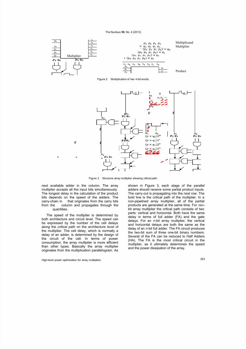
Figure 2. Multiplication of two 4-bit words.
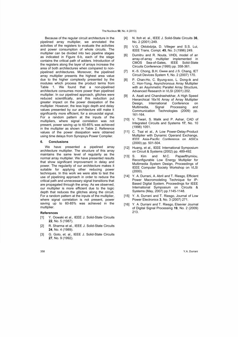
Figure 3. Structure array multiplier showing critical path.
next available adder in the column. The arraymultiplier accepts all the input bits simultaneously.The longest delay in the calculation of the productbits depends on the speed of the adders. The
carry-chain in that originates from the carry bitsfrom the column and propagates through the
quantities.
The speed of the multiplier is determined byboth architecture and circuit level. The speed canbe expressed by the number of the cell delaysalong the critical path on the architecture level ofthe multiplier. The cell delay, which is normally adelay of an adder, is determined by the design ofthe circuit of the cell. In terms of powerconsumption, the array multiplier is more efficientthan other types. Basically the array multiplier
originates from the multiplication parallelogram. As
shown in Figure 3, each stage of the paralleladders should receive some partial product inputs.The carry-out is propagating into the next row. Thebold line is the critical path of the multiplier. In a
non-pipelined array multiplier, all of the partialproducts are generated at the same time. For nxn-bit array multiplier the critical path consists of twoparts: vertical and horizontal. Both have the samedelay in terms of full adder (FA) and the gatedelays. For an n-bit array multiplier, the verticaland horizontal delays are both the same as thedelay of an n-bit full adder. The FA circuit producesthe two-bit sum of three one-bit binary numbers.Several of the FA can be reduced to Half Adders(HA). The FA is the most critical circuit in themultiplier, as it ultimately determines the speedand the power dissipation of the array.
+
F
000
F
F
F
++
F
F
F
F
F
Multiplicand
Multiplier
Product
Multiplier

8/10/2019 J High Level Power Optimization for Array Multipliers.pdf
http://slidepdf.com/reader/full/j-high-level-power-optimization-for-array-multiplierspdf 4/8
The Nucleus 50, No. 4 (2013)
354 Y.A. Durrani
Figure 4. A synchronous pipelined model.
In our experiments, instead of making onestraight forward 4×4-bit multiplication having eightbit result, it can carry out the multiplication in twosteps: First is the four 2×2 -bit multiplications
carried out, by creating four partial 4-bit products.These partial products are added together tocreate the final 8 -bit product. In our design there
are only three different type of non-complex blocksare needed to build up the entire multiplier. Theseblocks are Carry Propagate Adder (CPA), CarrySave Adder (CSA) and Multiplexer (MUX) asshown in figure 6-a. The four different partialproducts are created with the four multipliers withone CPA and four MUX blocks. Each MUX blockhas two bit input data while the CPA takes four bitinput data. All four inputs of the multiplexers arefour bit wide. The addition and the carry shift are
performed with two CSA and one CPA blocks,which permits the addition of the outputs of theright boundary adders. Each CPA and CSA blockhas six FA. The proposed architecture has theadvantage of low power consumption and the highoperating speed. Moreover, it occupies small areadue to the less number of transistors. Thisarchitecture is achieved at the circuit level byminimizing the number of internal nodecapacitances and reducing the switching activity inthe circuit.
3. Pipelined Array Multiplier
Pipelined multipliers are effective in systemswhere arithmetic throughput is more important thanthe latency. A linear pipeline processor is acascade of processing stages which are linearlyconnected to perform a fixed function over astream of data flowing from one end to the other.Our basic model of the synchronous pipelining isillustrated in Figure 4. The clocked registers areused to interface between different stages. Uponthe arrival of a clock pulse, all registers datatransfers simultaneously to the next stage.Successive tasks or operations are initiated oneclock per cycle to enter the pipeline. Once the
pipeline is filled, one result emerges from thepipeline for an additional cycle. This throughput issustained only if the successive tasks areindependent of each other. The clock cycle τ of a
pipeline is determined as: Let be the time delayof the circuitry in stage the setup time of the
register, and the Clock-to-Q delay. Denote the
maximum stage delay as , then:
( )max1
m i i
k
(5)
m s qT T
(6)
The pipeline frequency is defined as the inverseof the clock period:
1
f (7)
Ideally, a linear pipeline of k stages can process n
tasks in clock cycles, where k cyclesare needed to complete the execution of the veryfirst task and the remaining tasks require
cycles. Thus the total time is:
( 1)k T k n (8)
where τ is the clock period.
Behaviourally our proposed pipelined arraymultiplier is represented by a multiplier followed by
two stage registers shown in Figure 5a and thesummary of the Hardware Descriptive Language(HDL) code is demonstrated in Figure 5c. Themultiplier consists of eight breaking up inputadders in two sets of the adders with two stageregisters explained in Figure 5b. The HDL codingstyle can be helpful to improve the timings of thedata flow. We have implemented the two stagepipelined array multiplier as demonstrated inFigure 6b. Introduction of the registers increasesthe area of the architecture, when compared to thenon-pipelined architectures.
Combinational
LogicTd
Combinational
LogicTd
Input
Tq Ts Tq
Register
Output
Register Register

8/10/2019 J High Level Power Optimization for Array Multipliers.pdf
http://slidepdf.com/reader/full/j-high-level-power-optimization-for-array-multiplierspdf 5/8
The Nucleus 50, No. 4 (2013)
High-level power optimization for array multipliers 355
B
A
Clk
D Q
Clk
YD Q
Clk
Y1
(a) (b) (c)
Figure 5. (a) Visualizing pipelining (b) VHDL code for pipelining.
Figure 6. (a) Schematics of array multiplier, (b) Schematics of Pipelined array multiplier.
4. Power Macromodeling for Array Multiplier
Several approaches have been proposed toconstruct power macro-models using InternationalSymposium on Circuit and Systems (ISCAS-85)benchmark circuits [11-13]. We have observed thatthe same methodology works as well for different
blocks of array multipliers in terms of the statisticalknowledge of their primary I/O.
The power estimation procedure is illustrated inFigure 7. In the high-level flow, the first step is thelogic synthesis of the parameterized and structuralHDL description of the arithmetic modules. Forpower characterization, we considered only the
PipeMultProc : process
begin
wait until clk = '1';
Y1 <= A * B;
Y <= Y1;
end process;
MUX
MUX
MUX
CSA
CSA
CPA
R
Stage-1
R R R
R R R
MUX
CPA
Stage-2
CPA
MUX
MUX
MUX CSA
CSA
CPA
MUX

8/10/2019 J High Level Power Optimization for Array Multipliers.pdf
http://slidepdf.com/reader/full/j-high-level-power-optimization-for-array-multiplierspdf 6/8
The Nucleus 50, No. 4 (2013)
356 Y.A. Durrani
Figure 7. High-level characterization flow.
dynamic power dissipation, which forms thedominant component of the total power. In thesecond step, the switching activity per node vialogic-level simulation has been taken place tocompute the power for a certain input vector suchas:
2
1 i
N
load dd i i
Power C V fE (9)
Where is the capacitance at node i , is thepower supply voltage, f is the frequency and is the
activity factor at node i . The term of “(9)” is the
actually the number of transitions from logic „1‟ tologic „0‟ per time unit for the node i , which is equalto the ratio of number of node transitions from logic„1‟ to logic „0‟, divided by the total number of inputvectors:
1 0
1 0
#.
#
i
i
transf E f
vectors (10)
From “(9)” and “(10)” the power is:
N
i
load
dd
ii
transC vectors
V Power
1
01
2
##
(11)
The array multiplier is simulated under differentinput sample streams with the signal
probability . Signal probability is used foraccurate estimation of signal activity. Therefore it isessential to accurately calculate signal probabilityfor further use in estimating activity.
The P(x) in “(12)” of a node x in the circuitcorresponds to the average fraction of clock cycleswith a period of T in which the node has a steadystate logic value of ONE.
(12)
Given with the number of primary inputs r andthe input binary stream
Parameter VHDL
Description
Synthesis
Logic Level
Description
Logic Level
Simulation
Parameter Set
Target
Technology
Target
Technology
Switching Activity
per node
Area/Delay
Estimation
Capacitance
per node
Power Estimation

8/10/2019 J High Level Power Optimization for Array Multipliers.pdf
http://slidepdf.com/reader/full/j-high-level-power-optimization-for-array-multiplierspdf 7/8
The Nucleus 50, No. 4 (2013)
High-level power optimization for array multipliers 357
Table 1. Estimated area for the 4x4-bit multiplier.
Multiplier Area
4x4-Bit Multiplier 77494
4x4-Bit Pipelined Multiplier Stage-(1) 89434
4x4-Bit Pipelined Multiplier Stage-(2) 104166
Table 2. Power optimization of the 4x4-bit multiplier using two stage pipelining.
Non-PipelinedMultiplier
Pipelined Multiplier
Input SignalProbability
Power (mW)Stage-(1)
Power (mW)Stage-(1)
Power Optimization in %Stage-(2)
Power (mW)Stage-(2)
Power Optimization in %
0.125 0.7490 0.43424 72.48 0.4480 67.18
0.250 1.947 1.1555 68.49 1.2063 61.40
0.375 3.0628 1.7802 72.04 1.864 64.31
0.500 4.1441 2.2708 82.49 2.3812 74.03
0.625 4.8275 2.6061 85.23 2.739 76.25
0.750 4.5799 2.6728 71.35 2.8194 62.44
0.875 3.4788 2.5384 37.046 2.6793 29.83
of length s, the multiplier is simulated with eightdifferent signal probabilities with length of 1,000random vectors. The power measurements werenormalized by different operating frequencies.
5. Experimental Results
In this section, we show the results of ourpower optimization approach. We haveimplemented a pipelined array multiplier of simple
accumulation algorithm by HDL language asshown in Figure 6(a,b). During the characterizationphase, the average power consumption measuredusing power function f(.) in “(11)”, while leastsquare fitting is used to perform linear regression.The input chosen sequences are highly correlatedand they are generated by our new method. Theaccuracy is tested running gate-level and RTLsimulations. The power is estimated using MonteCarlo zero-delay simulation technique. Wecompare our power macro-modelling results
estimated P with Synopsys Power Compiler tool
simulated P and compute the average absolute and
maximum percentage errors using “(13)”.
100%simulated estimated
error
simulated
P P P
P (13)
The given input metrics values are moreaccurate for the specify range between [0.2, 0.8]and less accurate between [0, 0.2] and [0.8, 1].The minimum simulations length can bedetermined through convergence analysis.Converging on the average power figure help us toidentify the minimum length necessary for eachsimulation by considering when the powerconsumption gets close to a steady value given anarbitrary acceptance threshold. Also theconvergent sample size is not a function of circuitsize, it depends on how “widely” the powerdistributes. Regression analysis is performed to fitthe model‟s coefficients. For the non-pipelined andpipelined array multipliers, we measuredcorrelation coefficient 96% and 87%, respectively.
8/10/2019 J High Level Power Optimization for Array Multipliers.pdf
http://slidepdf.com/reader/full/j-high-level-power-optimization-for-array-multiplierspdf 8/8
The Nucleus 50, No. 4 (2013)
358 Y.A. Durrani
Because of the regular circuit architecture in thepipelined array multiplier, we annotated theactivities of the registers to evaluate the activities
and power consumption of whole circuits. Themultiplier can be divided into two pipeline stagesas indicated in Figure 6-b, each of the stagecontains the critical path of adders. Introduction ofthe registers along the layer of arrays increase thearea of both architectures when compared to non-pipelined architectures. Moreover, the pipelinedarray multiplier presents the highest area valuedue to the higher complexity presented by themodules which process the product terms fromTable 1. We found that a non-pipelinedarchitecture consumes more power than pipelinedmultiplier. In our pipelined approach, glitches were
reduced scientifically, and this reduction putgreater impact on the power dissipation of themultiplier. However, the less logic depth and delayvalues presented by our architecture still make itsignificantly more efficient, for a sinusoidal signal.For a random pattern at the inputs of themultipliers, where signal correlation was notpresent, power saving up to 60-85% was achievedin the multiplier as shown in Table 2. Referencevalues of the power dissipation were obtainedusing time delays from Synopsys Power Compiler.
6. Conclusions
We have presented a pipelined arrayarchitecture multiplier. The structure of this arraymaintains the same level of regularity as thenormal array multiplier. We have presented resultsthat show significant improvement in delay andpower. The regularity of our architecture makes itsuitable for applying other reducing powertechniques. In this work we were able to test theuse of pipelining approach in order to reduce thecritical path and unnecessary signal transitions thatare propagated through the array. As we observed,our multiplier is more efficient due to the logicdepth that reduces the glitches along the circuit.
For a random pattern at the inputs of the multiplier,where signal correlation is not present, powersaving up to 60-85% was achieved in themultiplier.
References
[1] Y. Oowaki et al., IEEE J. Solid-State Circuits22, No. 5 (1987).
[2] R. Sharma et al., IEEE J. Solid-State Circuits24, No. 4 (1989).
[3] G. Goto, et. al., IEEE J. Solid-State Circuits27, No. 9 (1992).
[4] N. Itoh et. al., IEEE J. Solid-State Circuits 36,No. 2 (2001) 249.
[5] V.G. Oklobdzija, D. Villeger and S.S. Lui,IEEE Trans. Compt. 45, No. 3 (1996) 249.
[6] Dumitru and R. Nouta, VHDL model of anarray-of-array multiplier implemented inCMOS Sea-of-Gates, IEEE Solid-StateCircuits Conference (1995) pp. 358-361.
[7] K.-S. Chong, B.H. Gwee and J.S. Chang, IETCircuit Devices System 1, No. 2 (2007) 170.
[8] P. Chan-Ho, C. Byung-soo, L. Dong-ik andC. Hon-Yong, Asynchronous Array Multiplierwith an Asymmetric Parallel Array Structure,
Advanced Research in VLSI (2001) 202.
[9] A. Asati and Chandrashekhar, A High SpeedHierarchical 16x16 Array of Array MultiplierDesign, International Conference onMultimedia, Signal Processing andCommunication Technologies (2009) pp.161-164.
[10] V. Tiwari, S. Malik and P. Ashar, CAD ofIntegrated Circuits and Systems 17, No. 10(1998) 1051.
[11] C. Tsai et al., A Low Power-Delay-ProductMultiplier with Dynamic Operand Exchange,IEEE Asia-Pacific Conference on ASICs(2000) pp. 501-504.
[12] Huang, et al., IEEE International Symposiumon Circuit & Systems (2002) pp. 489-492.
[13] S. Kim and M.C. Papaefthymiou,Reconfigurable Low Energy Multiplier forMultimedia System Design, Proceedings ofIEEE Computer Society Workshop on VLSI(2000).
[14] Y. A. Durrani, A. Abril and T. Riesgo, EfficientPower Macromodeling Technique for IP-Based Digital System. Proceedings for IEEEInternational Symposium on Circuits &Systems (May, 2007) pp.1145-1148.
[15] Y. A. Durrani and T. Riesgo, Journal of LowPower Electronics 3, No. 3 (2007) 271.
[16] Y. A. Durrani and T. Riesgo, Elsevier Journalof Digital Signal Processing 19, No. 2 (2009)
213.