Embed Size (px)
Citation preview
The Crystallization of Amorphous Aluminum Oxide Thin FilmsGrown on NiAl(100)
Hailang Qin,‡ Peter Sutter,§ and Guangwen Zhou‡,†
‡Department of Mechanical Engineering and Multidisciplinary Program in Materials Science and Engineering, State Universityof New York, Binghamton, New York 13902
§Center for Functional Nanomaterials, Brookhaven National Laboratory, Upton, New York 11973
The crystallization of amorphous aluminum oxide thin films
formed on NiAl(100) has been investigated using in-situ low
energy electron microscopy, low energy electron diffraction,and scanning tunneling microscopy. It is found that both the
annealing temperature and annealing time play crucial roles in
the crystallization process. A critical temperature range of450°C–500°C exists for the crystallization to occur within a
reasonably short annealing time. The initially uniform oxide
film first becomes roughened, followed by coalescing into amor-
phous-like oxide islands; further annealing results in the con-version of the amorphous oxide islands into crystalline oxide
stripes. The density of the crystalline oxide stripes increases
concomitantly with the decrease in the density of the amor-
phous oxide islands for annealing at a higher temperature orlonger time.
I. Introduction
ALUMINUM oxide thin films have important applicationsin microelectronics, protective coatings, and catalysis.
In particular, the formation of aluminum oxide on NiAl sub-strates has been studied extensively owing to its importantapplications in harsh environments ranging from high-tem-perature materials in propulsion systems and gas turbineengines to ambient-temperature reactions, such as surfacecatalysts and electronic metallization.1–14 The aluminum oxi-des on NiAl(100) were typically formed by directly oxidizinga clean NiAl(100) surface at a high temperature (typicallyaround 727°C or above) or by exposing a clean NiAl(100)surface to oxygen gas at room temperature followed byannealing at a high temperature, both of which would resultin fully- or partially crystallized oxides.9,10 Most of the stud-ies focused on investigating the properties of the crystallineoxides due to their stable electronic and geometric structures,with only a few exceptions focusing on the study of amor-phous aluminum oxides formed on NiAl(100) substrates. Forinstance, Gabmann et al.15,16 investigated the oxide structurewith electron energy loss spectroscopy after annealing theroom-temperature-oxidized surface at 427°C. An alterationof the local structure within the oxide film was suggested andthe structure of oxide film was still found to be differentfrom the crystallized oxide film formed after annealing at927°C. Using low-energy electron microscopy (LEEM),McCarty17 studied the crystallization of the amorphous oxidefilms formed by oxidation of NiAl(110) at 325°C and foundthat crystallized oxide domains and oxide-free regions
developed on the surface when the amorphous oxide wasannealed at 695°C and above. In addition to the aforemen-tioned studies on the amorphous aluminum oxide filmsformed from the oxidation of NiAl alloys, the crystallizationof amorphous Al2O3 thin films formed on silicon by atomiclayer deposition was studied using grazing-incidence X-raydiffraction, which indicates that decreasing oxide film thick-ness leads to a higher crystallization temperature.18 However,important information regarding the range of critical temper-atures at which the amorphous alumina films starts to crys-tallize and the associated film morphological evolution withinthe temperature range is still not elucidated. Thus far, thereare no detailed studies on the nucleation and growth of thecrystalline aluminum oxide out of the amorphous aluminafilms. In general, there is a lack of study on how an amor-phous oxide thin film transforms into a crystalline oxide,which is especially important in controlling both the morpho-logies and atomic structures of the oxide films, and thus theirelectrical and chemical properties.
In this article, the crystallization process of the amorphousaluminum oxide films formed on a clean NiAl(100) surface isstudied in detail using a combination of in-situ LEEM, lowenergy electron diffraction (LEED), and scanning tunnelingmicroscopy (STM). The oxide formed by room-temperatureoxygen exposure was annealed to different temperatures fordifferent time periods. The surface morphology evolution ofthe oxide films was characterized by both LEEM and STM,and the structure of the oxide films was characterized withLEED. A simple “time-temperature” map for the crystalliza-tion of Al2O3 thin films was obtained from the experimentalmeasurements.
II. Experimental Procedure
The STM and LEED experiments were performed in theSTM chamber and analysis chamber of an ultra-high vacuum(UHV) system from RHK Technology Inc (Troy, MI). Thebase pressures in the two chambers were about 7 9 10�11
and 2 9 10�10 Torr respectively. The single-crystal NiAl(100)substrate, purchased from Princeton Scientific Corp. (Prince-ton, NJ), has an orientation accuracy better than 0.1° to the(100) crystallographic orientation. For each cycle, the oxida-tion started with a freshly cleaned surface, which wasachieved by flashing the sample up to 1100°C–1200°C a fewtimes. Surface cleanliness and order were checked by Augerelectron spectroscopy, X-ray Photoelectron spectroscopy(XPS) and LEED. The oxidation was performed by exposingthe clean surface to oxygen gas at a partial pressure of1 9 10�7 Torr at room temperature for 100 s. The oxide filmformed under this condition has a thickness of ~3 �A, whichmay correspond to a monolayer of Al2�xO3, where x ~ 0.24,as determined from the XPS Al/O peak intensity ratio.19 Forthe first set of experiments, the sample temperature wasraised to 500°C, 600°C, 650°C, and 750°C, and the sample
N. Jacobson—contributing editor
Manuscript No. 34464. Received January 29, 2014; approved May 8, 2014.†Author towhom correspondence should be addressed. e-mail: [email protected]
2762
J. Am. Ceram. Soc., 97 [9] 2762–2769 (2014)
DOI: 10.1111/jace.13036
© 2014 The American Ceramic Society
Journal
was annealed for 5 min. The sample was annealed for30 min at each temperature for the second set of experi-ments. For another two sets, the sample was annealed at550°C for 2 h and 500°C for 4 h respectively. Both theLEED and STM measurements were performed after thesample cooled down to room temperature. The STM imagingwas performed with an electrochemically etched W tip andthe bias was applied on the sample.
The LEEM experiments were carried out in a separateUHV system with a base pressure of about 4 9 10�10 Torr.All the LEEM images were obtained in bright field mode.The sample was cleaned with the same method as the oneused for the STM and LEED measurement. The LEEMimages were taken in-situ while exposing the clean surface tooxygen gas at a partial pressure of 2 9 10�9 Torr at around250°C for about 100 s and while annealing the sample ateach specified temperature for a few minutes.
III. Results and Discussions
Figures 1(a)–(f) show a series of LEEM images taken fromthe clean surface, the surface after the O2 exposure at~250°C, and the surface after annealing at around 500°C,550°C, 600°C, and 800°C, respectively, each for several min-utes. As seen in Fig. 1(a), the clean surface shows a highdensity of slightly curved steps, and the step edges appear assharp dark lines in the LEEM images. As seen in Fig. 1(b),upon exposure to O2 gas at a partial pressure of2 9 10�9 Torr at ~250°C, the overall features of the NiAlsurface (i.e., the terrace width, step density and shape) arestill visible and remain relatively unchanged, but the sharpcontrast from the step edges became blurry. The entire sur-face shows a granular morphology, but the resolution in theLEEM images does not allow concluding that the oxide filmis amorphous (the nature of the amorphous oxide film isinferred by LEED as shown later). Our previous XPS studiesshowed that the oxide film formed on NiAl(100) under thesimilar oxidation conditions is an aluminum oxide and theSTM imaging showed that the oxide film has a relatively uni-form thickness on the average across the entire surface asinferred by unchanged step height (3 �A) across the differentsurface terraces before and after the oxidation.19 However, itis worth mentioning that the oxide film shows local varia-tions in surface height due to the granular morphology at thenanoscale, i.e., the film thickness varies locally. The oxidizedsurface was then annealed at different temperatures and thesurface morphological evolution was monitored by in-situLEEM imaging during the annealing process. No noticeablechanges in the surface morphology were observed until theannealing temperature reached 500°C. Figure 1(c) is an in-situ LEEM image from the surface after being annealed at500°C for a few min, which shows that the dark line contrastfrom the step edges completely disappeared and the initiallyrelatively uniform oxide film developed into coarsened grains(as shown later by LEED and STM, these coarsened grainsare still amorphous, crystallized oxide grains show a muchregular stripe morphology). Figure 1(d) reveals coarsening ofthe grains, which became more prominent after annealing at550°C. Figure 1(e) shows that some stripe-like structuresstarted to appear at 600°C; however, the details are notaccessible at this point, because the size of these structureswas too small to be resolved by LEEM imaging. Upon fur-ther annealing at higher temperatures, more stripes wereformed. An example of the LEEM image of the surface afterannealing at about 800°C is shown in Fig. 1(f), which revealsa high density of oxide stripes are uniformly distributedacross the entire surface.
The in-situ LEEM observations described above demon-strate that the initially relatively uniform oxide film tends toform coarsened grains at the annealing temperature ofaround 500°C and that the crystallized oxide films have astripe-like morphology. To gain a better understanding of
the crystallization process, LEED and STM studies were per-formed to acquire more details on the morphology and struc-ture of the oxide films during the amorphous-crystallinetransition upon annealing. Figures 2(a) and (b) show theLEED patterns of the clean NiAl(100) surface and the sur-face after exposure to oxygen gas with a pressure ofpO2 = 1 9 10�7 Torr at room temperature for 100 s. Theclean-surface LEED patterns show that the clean surface hada c(3
ffiffiffi
2p � ffiffiffi
2p
;ffiffiffi
2p � 3
ffiffiffi
2p
)R45° reconstruction20,21 and itthen changed to the (1 9 1) structure of the NiAl(100) sub-strate with significantly reduced intensity of the diffractionspots after the oxygen exposure. This indicates that the c(3
ffiffiffi
2p � ffiffiffi
2p
;ffiffiffi
2p � 3
ffiffiffi
2p
)R45° surface reconstruction of theNiAl(100) substrate was destroyed after the oxygen exposureand the surface was fully (or almost fully) covered by anamorphous oxide film. One can note that the LEED patternof the clean NiAl(100) surface shows quite high backgroundintensity. It may be caused by the presence of randomlydistributed surface defects that varies with annealing condi-tion, as discussed by Blum et al.9 The schematic of theLEED pattern showing the (191) substrate, the c(3
ffiffiffi
2p � ffiffiffi
2p
;ffiffiffi
2p � 3
ffiffiffi
2p
)R45° surface reconstruction on theclean surface, and the (2 9 1, 1 9 2) oxide superstructure isshown in Fig. 2(c).
Scanning tunneling microscopy images and the corre-sponding LEED patterns for the first set of the annealingexperiment (i.e., annealing for 5 min) are shown inFigs. 3(a)–(d). As can be seen in the inset LEED pattern inFig. 3(a), the substrate spots are still visible, but their intensi-
(a)
(c)
(b) (e)
(f)
(d)
Fig. 1. Low-energy electron microscopy images (size:(7.5 lm 9 7.5 lm) of NiAl(100): (a) before, (b) after O2 exposure,(c) after annealing at 500°C, (d) 550°C, (e) 600°C, and (f) 800°C fora few min respectively. The drift is noticeable in the images. The twodarks spots are the damages on the channel plate.
September 2014 Crystallization of Amorphous 2763

ties were further reduced after the oxide film was annealed at500°C for 5 min. As revealed by the LEEM images shown inFig. 1 and the STM images in Fig. 3, one can note that theamorphous oxide films show an irregular granular featurewhile crystallized oxide films show a much regular stripemorphology. In addition to the LEED pattern, their distinctdifferences in the morphologies provides additional insightinto the crystallization process. Although the STM imagesstill show irregular granular amorphous feature, the surfacestarted to form tiny islands (still amorphous oxide asrevealed by the LEED pattern), and this causes the increased
surface roughness22 compared to the initially uniform oxidefilm formed right after room temperature oxygen exposure.The observed surface morphological evolution is consistentwith the in-situ LEEM observations shown in Fig. 1(c). Theinset LEED pattern in Fig. 3(b) obtained from the oxide filmannealed at 600°C for 5 min showed stronger substrate spotsand very weak intensities around the (2 9 1, 1 9 2) locationsassociated with a crystalline oxide phase.16 The streaks in theLEED pattern of crystalline oxides formed on NiAl(100) arecommonly observed by others and are usually attributed tothe loss of ordering in the oxide film in the corresponding
(a) (c)(b)
Fig. 2. Low energy electron diffraction (LEED) patterns of (a) the clean NiAl(100) surface, and (b) the NiAl(100) surface after exposure tooxygen of 1 9 10�7 Torr at room temperature for 100 s. Primary electron energy: EP = 121 eV. (c) Schematic of the LEED pattern showing the(1 9 1) substrate, the c(3
ffiffiffi
2p � ffiffiffi
2p
;ffiffiffi
2p � 3
ffiffiffi
2p
)R45° reconstruction on the clean surface, and the (2 9 1, 1 9 2) oxide superstructure with streaks.The streaks are not shown in the schematic.
(a) (c)
(b) (d)
Fig. 3. Scanning tunneling microscopy images (Vsample = �1V, It = 1nA.) after annealing for 5 min at (a) 500°C, (b) 600°C, (c) 650°C, and (d)750°C respectively. The insets are the corresponding LEED patterns taken at a primary electron energy of EP = 131 eV for (a)–(c) and 113 eVfor (d).
2764 Journal of the American Ceramic Society—Qin et al. Vol. 97, No. 9

surface direction.16,23 The STM image shows that theannealed surface has now developed a significant amount ofoxide islands. These oxide islands, however, did not showany long-range order, as evidenced by the lack of strongintensity of diffraction associated with the crystalline oxidephase. Figure 4(a) is a zoom-in STM image from these areasshown in Fig. 3(b) and it reveals that a small amount ofcrystalline thin oxide stripes had already formed, which likely
gave rise to the weak intensity at the (2 9 1, 2 9 1) locationsas shown in the inset LEED pattern in Fig. 3(b). With fur-ther (added on) annealing at 650°C for 5 min, pronouncedintensities appear at the (2 9 1, 2 9 1) locations as shown inthe inset LEED pattern in Fig. 3(c), suggesting the formationof a non-negligible amount of crystalline oxides. This is alsosupported by the STM image in Fig. 3(c) and its enlargedview in Fig. 4(b), which show that more oxide stripes were
(a) (b)
Fig. 4. Scanning tunneling microscopy images (Vsample = �1V, It = 1nA) of the oxide surface after annealing at (a) 600°C and (b) 650°C for5 min respectively.
(a) (c)
(b) (d)
Fig. 5. Scanning tunneling microscopy images (Vsample = �1 V, It = 1nA, area: 100 nm 9 100 nm.) after annealing at (a) 500°C, (b) 600°C, (c)650°C, and (d) 750°C for 30 min respectively. The insets are the corresponding low energy electron diffraction patterns taken at a primaryelectron energy of EP = 131 eV.
September 2014 Crystallization of Amorphous 2765

developed on the surface. After annealing at 750°C for5 min, the c(3
ffiffiffi
2p � ffiffiffi
2p
;ffiffiffi
2p � 3
ffiffiffi
2p
)R45° spots associatedwith the clean NiAl(100) substrate re-appeared at low pri-mary electron energies, e.g., 113 eV, which indicates thatsome nonoxidized areas appeared. One likely cause for thereappearance of the diffraction spots associated with the non-oxidized surface is that the initially uniform amorphous alu-mina film was broken into amorphous islands, which thentransformed to crystalline alumina stripes, resulting inexposed oxide-free NiAl areas having the c(3
ffiffiffi
2p � ffiffiffi
2p
;ffiffiffi
2p � 3
ffiffiffi
2p
)R45° reconstruction. This is also sup-ported by the formation of surface depressions (which can beas deep as 0.6–0.8 nm), as observed from the annealed sur-face [Figs. 3(c) and (d)]. However, we cannot exclude thepossibility that the c(3
ffiffiffi
2p � ffiffiffi
2p
;ffiffiffi
2p � 3
ffiffiffi
2p
)R45° reconstruc-tion may reform at the alloy/oxide interface during annealingowning to the supply of Al atoms from the bulk to the alloy/oxide interface that was depleted in Al by the oxide growthat room temperature.
It is shown in the preceding discussions that the amor-phous aluminum oxide films started to crystallize at anannealing temperature of ~500°C and the amorphous-to-crys-talline transformation occurred via an island formation pro-cess by breaking up the initially uniform amorphous oxidefilm. On the other hand, the annealing time could also be animportant factor in the crystallization. To explore the effectof annealing time, a similar set of experiment was carried outwith an annealing time of 30 min at each temperature. TheSTM images and the corresponding LEED patterns are pre-sented in Figs. 5(a)–(d). The surface after annealing at 500°Cfor 30 min was still dominated by the amorphous-like oxideislands, as evidenced by both LEED and STM. In addition,the STM image shows that the surface roughness increasedfurther compared to the one after annealing for 5 min at thesame temperature. The longer annealing time led to thecoarsening of the amorphous oxide islands. After annealingat 600°C for 30 min, the LEED pattern shows a clear(2 9 1, 2 9 1) superstructure, indicating the formation ofcrystalline oxide stripes. From the STM image in Fig. 5(b), itcan be seen that both the amorphous oxide islands (whichhave less well-defined shapes) and the crystalline oxide stripesco-exist on the annealed surface. Comparing Figs. 3(b) and5(b), we find that the density of the amorphous oxide islandsdecreases with increasing the annealing time. Further anneal-ing at 650°C for 30 min significantly reduced the density andsizes of the amorphous oxide islands. Meanwhile, the densityof crystalline oxide stripes increased appreciably, with themajority of the surface being covered by thin stripes. Afterannealing at 750°C, the amorphous oxide islands almost dis-appeared and about 40% of the surface was covered by theoxide stripes, some of which are very thin ones. The corre-lated size and density evolution between the amorphousoxide islands and the crystalline oxide stripes indicates thatthe crystallization occurred via progressive consumption ofthe parent amorphous oxide.
To better illustrate the surface roughness and island sizechanges during the crystallization process, typical line profilesand the root-mean-square (standard deviations) roughness ofthe images from the oxide films before annealing, annealedat 500°C for 5 min, 30 min, and 4 h are plotted in Figs. 6(a)and (b) respectively. It can be seen that the root-mean-square(RMS) roughness did not change significantly after annealingat 500°C for 5 min, but increased to 0.7 �A after annealingfor 30 min and became 0.9 �A after annealing for 4 h (notadded-on). Furthermore, the island lateral size increasedaccordingly with the annealing time.
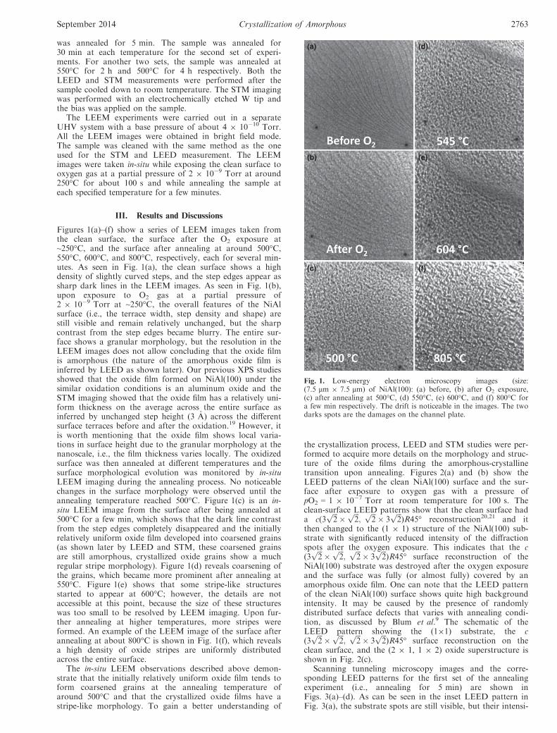
From the set of results on the samples annealed for 5 minfor each specified temperature, it is noted that the tempera-ture plays a crucial role in driving the amorphous oxide tocrystallize. For instance, a clear crystallization only startedafter annealing at 650°C, not much occurred at 500°C, oreven at 600°C. However, with increasing the annealing time
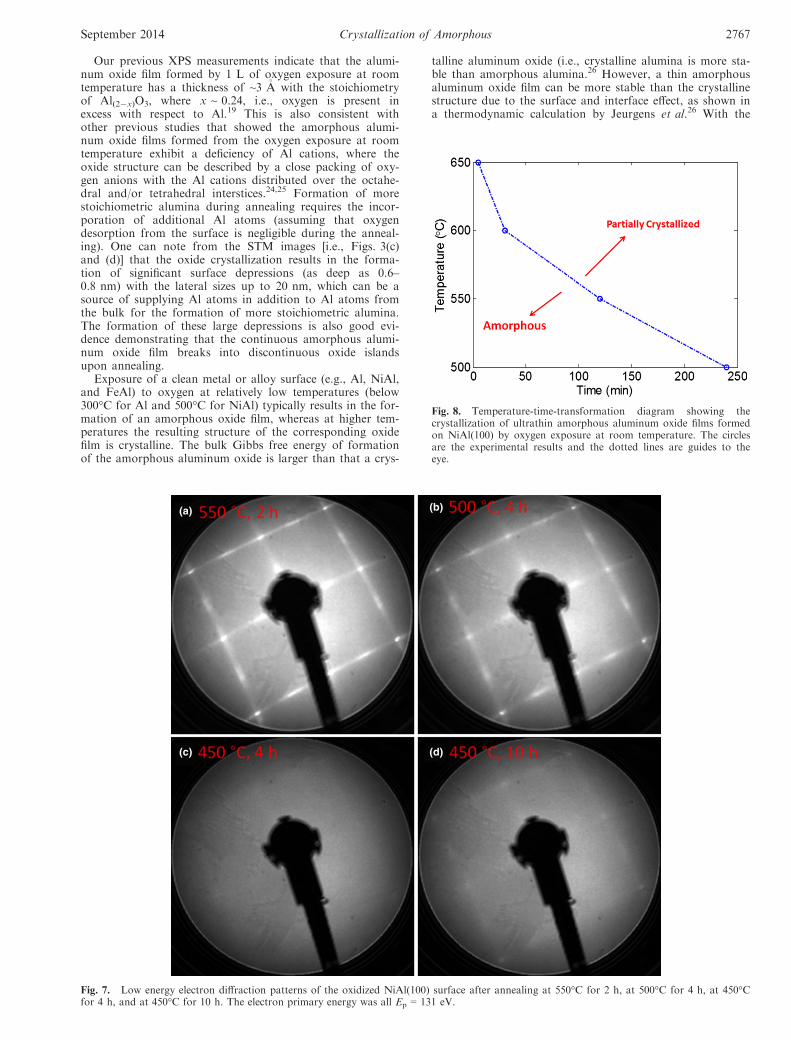
to 30 min for each temperature, clear crystallization startedto develop at even 600°C. In fact, the amorphous-to-crystal-line transformation could start at even a lower temperature.Figs. 7(a) and (b) show the LEED patterns obtained fromthe oxide films annealed at 550°C for 2 h and 500°C for 4 hrespectively. Both of these LEED patterns indicate that the(2 9 1, 2 9 1) oxide superstructure had already formed afterthe relatively long-time annealing. However, at 450°C, noclear crystallization occurred after annealing for 4 h, or evenfor 10 h, as shown in the LEED patterns in Figs. 7(c) and(d). This implies that the temperature range of 450°C–500°Cis the critical temperature range for the crystallization pro-cess to occur within a reasonably short annealing time. Thefindings on the crystallization condition are summarized inthe temperature-time-transformation diagram in Fig. 8,which shows that both the annealing temperature andannealing time play critical roles in the crystallization of thethin aluminum oxide films. For some of the annealing tem-peratures, shorter annealing times were not tested, thus thecrystallization may start earlier as shown in the figure.
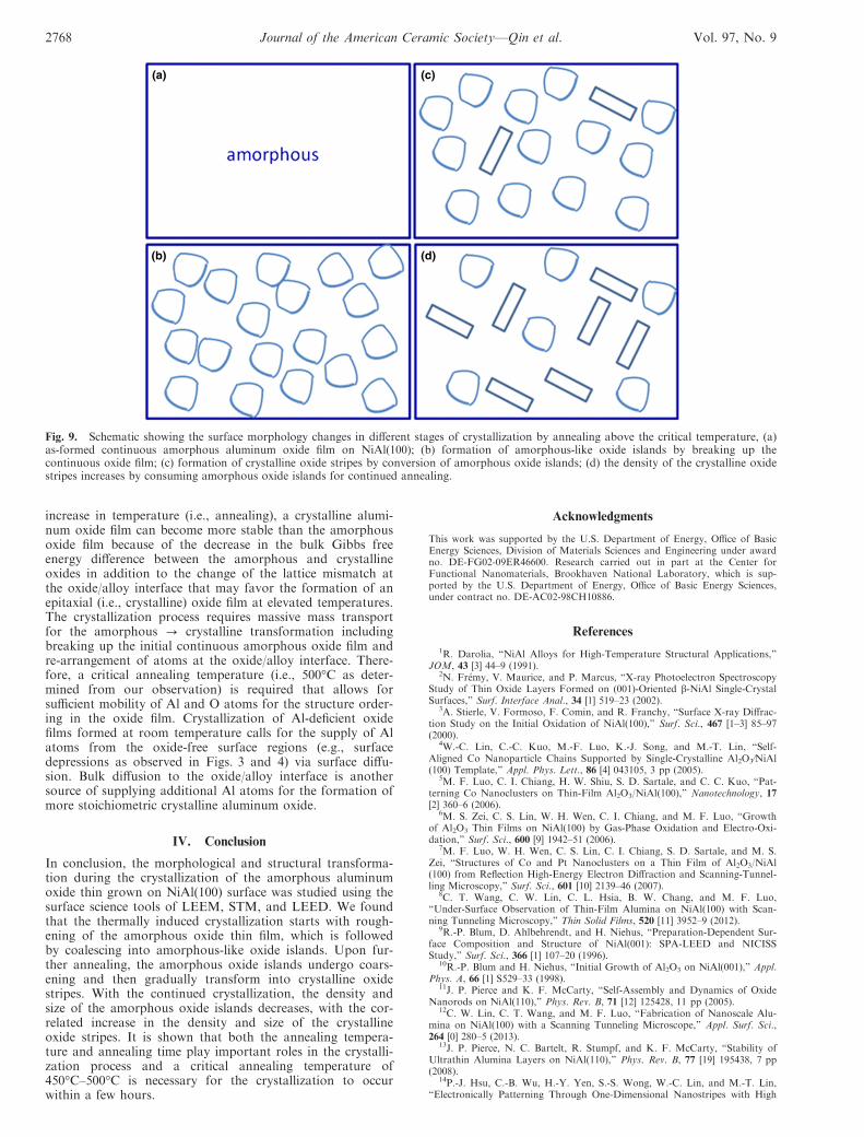
Figures 9(a)–(d) show schematically the crystallizationprocess. Upon annealing at high temperature, the initiallyuniform amorphous oxide film starts to become roughened.With further annealing at higher temperature or longer timeabove the critical temperature, amorphous-like oxide islandsstart to form by coalescence of the amorphous granularoxide film and correspondingly resulting in exposed NiAlsurface areas or thinner oxide areas. Further annealing leadsto the conversion of the amorphous oxide islands to crystal-line oxide stripes.
(a)
(b)
Fig. 6. (a) Line profiles and (b) RMS roughness of the surfacebefore annealing, and annealed at 500°C for 5 min, 30 min, and 4 h(240 min).
2766 Journal of the American Ceramic Society—Qin et al. Vol. 97, No. 9
Our previous XPS measurements indicate that the alumi-num oxide film formed by 1 L of oxygen exposure at roomtemperature has a thickness of ~3 �A with the stoichiometryof Al(2�x)O3, where x ~ 0.24, i.e., oxygen is present inexcess with respect to Al.19 This is also consistent withother previous studies that showed the amorphous alumi-num oxide films formed from the oxygen exposure at roomtemperature exhibit a deficiency of Al cations, where theoxide structure can be described by a close packing of oxy-gen anions with the Al cations distributed over the octahe-dral and/or tetrahedral interstices.24,25 Formation of morestoichiometric alumina during annealing requires the incor-poration of additional Al atoms (assuming that oxygendesorption from the surface is negligible during the anneal-ing). One can note from the STM images [i.e., Figs. 3(c)and (d)] that the oxide crystallization results in the forma-tion of significant surface depressions (as deep as 0.6–0.8 nm) with the lateral sizes up to 20 nm, which can be asource of supplying Al atoms in addition to Al atoms fromthe bulk for the formation of more stoichiometric alumina.The formation of these large depressions is also good evi-dence demonstrating that the continuous amorphous alumi-num oxide film breaks into discontinuous oxide islandsupon annealing.
Exposure of a clean metal or alloy surface (e.g., Al, NiAl,and FeAl) to oxygen at relatively low temperatures (below300°C for Al and 500°C for NiAl) typically results in the for-mation of an amorphous oxide film, whereas at higher tem-peratures the resulting structure of the corresponding oxidefilm is crystalline. The bulk Gibbs free energy of formationof the amorphous aluminum oxide is larger than that a crys-
talline aluminum oxide (i.e., crystalline alumina is more sta-ble than amorphous alumina.26 However, a thin amorphousaluminum oxide film can be more stable than the crystallinestructure due to the surface and interface effect, as shown ina thermodynamic calculation by Jeurgens et al.26 With the
(a)
(c)
(b)
(d)
Fig. 7. Low energy electron diffraction patterns of the oxidized NiAl(100) surface after annealing at 550°C for 2 h, at 500°C for 4 h, at 450°Cfor 4 h, and at 450°C for 10 h. The electron primary energy was all Ep = 131 eV.
Fig. 8. Temperature-time-transformation diagram showing thecrystallization of ultrathin amorphous aluminum oxide films formedon NiAl(100) by oxygen exposure at room temperature. The circlesare the experimental results and the dotted lines are guides to theeye.
September 2014 Crystallization of Amorphous 2767
increase in temperature (i.e., annealing), a crystalline alumi-num oxide film can become more stable than the amorphousoxide film because of the decrease in the bulk Gibbs freeenergy difference between the amorphous and crystallineoxides in addition to the change of the lattice mismatch atthe oxide/alloy interface that may favor the formation of anepitaxial (i.e., crystalline) oxide film at elevated temperatures.The crystallization process requires massive mass transportfor the amorphous ? crystalline transformation includingbreaking up the initial continuous amorphous oxide film andre-arrangement of atoms at the oxide/alloy interface. There-fore, a critical annealing temperature (i.e., 500°C as deter-mined from our observation) is required that allows forsufficient mobility of Al and O atoms for the structure order-ing in the oxide film. Crystallization of Al-deficient oxidefilms formed at room temperature calls for the supply of Alatoms from the oxide-free surface regions (e.g., surfacedepressions as observed in Figs. 3 and 4) via surface diffu-sion. Bulk diffusion to the oxide/alloy interface is anothersource of supplying additional Al atoms for the formation ofmore stoichiometric crystalline aluminum oxide.
IV. Conclusion
In conclusion, the morphological and structural transforma-tion during the crystallization of the amorphous aluminumoxide thin grown on NiAl(100) surface was studied using thesurface science tools of LEEM, STM, and LEED. We foundthat the thermally induced crystallization starts with rough-ening of the amorphous oxide thin film, which is followedby coalescing into amorphous-like oxide islands. Upon fur-ther annealing, the amorphous oxide islands undergo coars-ening and then gradually transform into crystalline oxidestripes. With the continued crystallization, the density andsize of the amorphous oxide islands decreases, with the cor-related increase in the density and size of the crystallineoxide stripes. It is shown that both the annealing tempera-ture and annealing time play important roles in the crystalli-zation process and a critical annealing temperature of450°C–500°C is necessary for the crystallization to occurwithin a few hours.
Acknowledgments
This work was supported by the U.S. Department of Energy, Office of BasicEnergy Sciences, Division of Materials Sciences and Engineering under awardno. DE-FG02-09ER46600. Research carried out in part at the Center forFunctional Nanomaterials, Brookhaven National Laboratory, which is sup-ported by the U.S. Department of Energy, Office of Basic Energy Sciences,under contract no. DE-AC02-98CH10886.
References
1R. Darolia, “NiAl Alloys for High-Temperature Structural Applications,”JOM, 43 [3] 44–9 (1991).
2N. Fr�emy, V. Maurice, and P. Marcus, “X-ray Photoelectron SpectroscopyStudy of Thin Oxide Layers Formed on (001)-Oriented b-NiAl Single-CrystalSurfaces,” Surf. Interface Anal., 34 [1] 519–23 (2002).
3A. Stierle, V. Formoso, F. Comin, and R. Franchy, “Surface X-ray Diffrac-tion Study on the Initial Oxidation of NiAl(100),” Surf. Sci., 467 [1–3] 85–97(2000).
4W.-C. Lin, C.-C. Kuo, M.-F. Luo, K.-J. Song, and M.-T. Lin, “Self-Aligned Co Nanoparticle Chains Supported by Single-Crystalline Al2O3∕NiAl(100) Template,” Appl. Phys. Lett., 86 [4] 043105, 3 pp (2005).
5M. F. Luo, C. I. Chiang, H. W. Shiu, S. D. Sartale, and C. C. Kuo, “Pat-terning Co Nanoclusters on Thin-Film Al2O3/NiAl(100),” Nanotechnology, 17[2] 360–6 (2006).
6M. S. Zei, C. S. Lin, W. H. Wen, C. I. Chiang, and M. F. Luo, “Growthof Al2O3 Thin Films on NiAl(100) by Gas-Phase Oxidation and Electro-Oxi-dation,” Surf. Sci., 600 [9] 1942–51 (2006).
7M. F. Luo, W. H. Wen, C. S. Lin, C. I. Chiang, S. D. Sartale, and M. S.Zei, “Structures of Co and Pt Nanoclusters on a Thin Film of Al2O3/NiAl(100) from Reflection High-Energy Electron Diffraction and Scanning-Tunnel-ling Microscopy,” Surf. Sci., 601 [10] 2139–46 (2007).
8C. T. Wang, C. W. Lin, C. L. Hsia, B. W. Chang, and M. F. Luo,“Under-Surface Observation of Thin-Film Alumina on NiAl(100) with Scan-ning Tunneling Microscopy,” Thin Solid Films, 520 [11] 3952–9 (2012).
9R.-P. Blum, D. Ahlbehrendt, and H. Niehus, “Preparation-Dependent Sur-face Composition and Structure of NiAl(001): SPA-LEED and NICISSStudy,” Surf. Sci., 366 [1] 107–20 (1996).
10R.-P. Blum and H. Niehus, “Initial Growth of Al2O3 on NiAl(001),” Appl.Phys. A, 66 [1] S529–33 (1998).
11J. P. Pierce and K. F. McCarty, “Self-Assembly and Dynamics of OxideNanorods on NiAl(110),” Phys. Rev. B, 71 [12] 125428, 11 pp (2005).
12C. W. Lin, C. T. Wang, and M. F. Luo, “Fabrication of Nanoscale Alu-mina on NiAl(100) with a Scanning Tunneling Microscope,” Appl. Surf. Sci.,264 [0] 280–5 (2013).
13J. P. Pierce, N. C. Bartelt, R. Stumpf, and K. F. McCarty, “Stability ofUltrathin Alumina Layers on NiAl(110),” Phys. Rev. B, 77 [19] 195438, 7 pp(2008).
14P.-J. Hsu, C.-B. Wu, H.-Y. Yen, S.-S. Wong, W.-C. Lin, and M.-T. Lin,“Electronically Patterning Through One-Dimensional Nanostripes with High
(a) (c)
(b) (d)
Fig. 9. Schematic showing the surface morphology changes in different stages of crystallization by annealing above the critical temperature, (a)as-formed continuous amorphous aluminum oxide film on NiAl(100); (b) formation of amorphous-like oxide islands by breaking up thecontinuous oxide film; (c) formation of crystalline oxide stripes by conversion of amorphous oxide islands; (d) the density of the crystalline oxidestripes increases by consuming amorphous oxide islands for continued annealing.
2768 Journal of the American Ceramic Society—Qin et al. Vol. 97, No. 9

Density of States on Single-Crystalline Al2O3 Domain,” Appl. Phys. Lett., 93[14] 143104, 3 pp (2008).
15P. Gaßmann, R. Franchy, and H. Ibach, “Preparation of a Well OrderedAluminum Oxide Layer on NiAl(001),” J. Electron Spectrosc. Relat. Phenom.,64–65 [0] 315–20 (1993).
16P. Gassmann, R. Franchy, and H. Ibach, “Investigations on Phase Transi-tions Within Thin Al2O3 Layers on NiAl(001) — HREELS on AluminumOxide Films,” Surf. Sci., 319 [1–2] 95–109 (1994).
17K. F. McCarty, “Imaging the Crystallization and Growth of OxideDomains on the NiAl(100) Surface,” Surf. Sci., 474 [1–3] L165–72 (2001).
18S. Jakschik, U. Schroeder, T. Hecht, M. Gutsche, H. Seidl, and J. W. Bar-tha, “Crystallization Behavior of Thin ALD-Al2O3 Films,” Thin Solid Films,425, 216–20 (2003).
19N. Cai, H. Qin, X. Tong, and G. Zhou, “Growth of Ultrathin AmorphousAlumina Films During the Oxidation of NiAl(100),” Surf. Sci., 618, 20–6(2013).
20N. Fr�emy, V. Maurice, and P. Marcus, “Initial Stages of Growth of Alu-mina on NiAl(001) at 1025 K,” J. Am. Ceram. Soc., 86 [4] 669–75 (2003).
21V. Maurice, N. Fr�emy, and P. Marcus, “Hydroxylation-Induced Modifica-tions of the Al2O3/NiAl(001) Surface at Low Water Vapour Pressure,” Surf.Sci., 581 [1] 88–104 (2005).
22H. Qin and G. Zhou, “The Formation of Double-Row Oxide Stripes Dur-ing the Initial Oxidation of NiAl(100),” J. Appl. Phys., 114 [8] 083513, 5 pp(2013).
23R.-P. Blum, D. Ahlbehrendt, and H. Niehus, “Growth of Al2O3 Stripes inNiA(001),” Surf. Sci., 396 [13] 176–88 (1998).
24L. P. H. Jeurgens, W. G. Sloof, F. D. Tichelaar, and E. J. Mittemeijer,“Structure and Morphology of Aluminium-Oxide Films Formed by ThermalOxidation of Aluminium,” Thin Solid Films, 418 [2] 89–101 (2002).
25L. P. H. Jeurgens, W. G. Sloof, F. D. Tichelaar, and E. J. Mittemeijer,“Growth Kinetics and Mechanisms of Aluminum-Oxide Films Formed byThermal Oxidation of Aluminum,” J. Appl. Phys., 92 [3] 1649–56 (2002).
26L. P. H. Jeurgens, W. G. Sloof, F. D. Tichelaar, and E. J. Mittemeijer,“Thermodynamic Stability of Amorphous Oxide Films on Metals: Applicationto Aluminum Oxide Films on Aluminum Substrates,” Phys. Rev. B, 62 [7]4707–19 (2000). h
September 2014 Crystallization of Amorphous 2769


![Density functional theory study of O–H and C–H bond …ws.binghamton.edu/me/Zhou/Zhou-publications/Surface...simulation package (VASP) [42–45] with the PW91 generalized gradient](https://img.dokumen.tips/doc/110x75/5b03edfe7f8b9a89208ce38f/density-functional-theory-study-of-oh-and-ch-bond-ws-package-vasp-4245.jpg)