Embed Size (px)
Citation preview

1. General description
The ISP1505 is a Universal Serial Bus (USB) high-speed host and peripheral transceiverthat is fully compliant with Universal Serial Bus Specification Rev. 2.0 and UTMI+ Low PinInterface (ULPI) Specification Rev. 1.1.
The ISP1505 can transmit and receive USB data at high-speed (480 Mbit/s), full-speed(12 Mbit/s) and low-speed (1.5 Mbit/s), and provides a pin-optimized, physical layerfront-end attachment to USB host, peripheral and OTG devices.
It is ideal for use in portable electronic devices, such as mobile phones, digital stillcameras, digital video cameras, Personal Digital Assistants (PDAs) and digital audioplayers. It allows USB Application-Specific Integrated Circuits (ASICs), ProgrammableLogic Devices (PLDs) and any system chip set to interface with the physical layer of theUSB through a 12-pin interface.
The ISP1505 can interface to the link with digital I/O voltages in the range of1.65 V to 3.6 V.
The ISP1505 is available in HVQFN24 package.
2. Features
n Fully complies with:
u Universal Serial Bus Specification Rev. 2.0u UTMI+ Low Pin Interface (ULPI) Specification Rev. 1.1
n Interfaces to host and peripheral cores; optimized for stand-alone and embedded hostapplications with an external VBUS supply; stand-alone peripheral cores, and SessionRequest Protocol (SRP)-capable peripheral cores
n Complete Hi-Speed USB physical front-end solution that supports high-speed(480 Mbit/s), full-speed (12 Mbit/s) and low-speed (1.5 Mbit/s)
u Integrated 45 Ω ± 10 % high-speed termination resistors, 1.5 kΩ ± 5 % full-speeddevice pull-up resistor, and 15 kΩ ± 5 % host termination resistors
u Integrated parallel-to-serial and serial-to-parallel converters to transmit and receive
u USB clock and data recovery to receive USB data at ±500 ppm
u Insertion of stuff bits during transmit and discarding of stuff bits during receive
u Non-Return-to-Zero Inverted (NRZI) encoding and decoding
u Supports bus reset, suspend, resume and high-speed detection handshake (chirp)
n Supports SRP for reduced power consumption
u Complete control over bus resistors
u Data line and VBUS pulsing session request methods
ISP1505A; ISP1505CULPI Hi-Speed Universal Serial Bus host and peripheraltransceiverRev. 01 — 19 October 2006 Product data sheet

NXP Semiconductors ISP1505A; ISP1505CULPI HS USB host and peripheral transceiver
u Integrated VBUS voltage comparators
n Highly optimized ULPI-compliant interface
u 60 MHz, 8-bit interface between the core and the transceiver
u Supports both 60 MHz input clock and 60 MHz output clock configurations
u Integrated Phase-Locked Loop (PLL) with auto-configuring support for 60 MHzinput clock, or one crystal or clock frequency: 19.2 MHz (ISP1505ABS), 26 MHz(ISP1505CBS)
u Fully programmable ULPI-compliant register set
u Internal Power-On Reset (POR) circuit
n Flexible system integration and very low current consumption, optimized for portabledevices
u Power-supply input range is 3.0 V to 3.6 V
u Internal voltage regulator supplies 3.3 V and 1.8 V
u Supports external VBUS charge pump
u External VBUS source is controlled using the PSW_N pin; open-drain PSW_Nallows per-port or ganged power control
u FAULT input pin to monitor the external VBUS supply status
u Supports wide range interfacing I/O voltage of 1.65 V to 3.6 V; separate I/O voltagepins minimize crosstalk
u Typical operating current of 10 mA to 48 mA, depending on the USB speed andbus utilization
u Typical suspend current of 35 µA
n Full industrial grade operating temperature range from −40 °C to +85 °Cn 4 kV ElectroStatic Discharge (ESD) protection on pins DP, DM, VBUS and GND
n Available in a small HVQFN24 (4 mm × 4 mm) Restriction of Hazardous Substances(RoHS) compliant, halogen-free and lead-free package
3. Applications
n Digital still camera
n Digital TV
n Digital Video Disc (DVD) recorder
n External storage device, for example:
u Zip drive
u Magneto-Optical (MO) drive
u Optical drive: CD-ROM, CD-RW, DVD
n Mobile phone
n MP3 player
n PDA
n Printer
n Scanner
n Set-Top Box (STB)
n Video camera
ISP1505A_ISP1505C_1 © NXP B.V. 2006. All rights reserved.
Product data sheet Rev. 01 — 19 October 2006 2 of 78

NXP Semiconductors ISP1505A; ISP1505CULPI HS USB host and peripheral transceiver
4. Ordering information
[1] The package marking is the first line of text on the IC package and can be used for IC identification.
Table 1. Ordering information
Part Package
Type number Marking Crystal orclockfrequency
Name Description Version
ISP1505ABS 05A[1] 19.2 MHz HVQFN24 plastic thermal enhanced very thin quad flat package;no leads; 24 terminals; body 4 × 4 × 0.85 mm
SOT616-1
ISP1505CBS 05C[1] 26 MHz HVQFN24 plastic thermal enhanced very thin quad flat package;no leads; 24 terminals; body 4 × 4 × 0.85 mm
SOT616-1
ISP1505A_ISP1505C_1 © NXP B.V. 2006. All rights reserved.
Product data sheet Rev. 01 — 19 October 2006 3 of 78

NXP Semiconductors ISP1505A; ISP1505CULPI HS USB host and peripheral transceiver
5. Block diagram
Fig 1. Block diagram
REGISTERMAP
ULPIINTERFACE
CONTROLLER
USB DATA SERIALIZER
USB DATA DESERIALIZER
HIGH-SPEED USB ATX
DM
DPSTP
DIR
NXT
DATA[7:0]
8
5
6
16
15
14
1, 2, 17 to 20, 22, 24
004aaa587
CLOCK21
TERMINATIONRESISTORS
VBUSCOMPARATORS
SRP CHARGEAND DISCHARGE
RESISTORS
POWER-ONRESET
PLL
CRYSTALOSCILLATOR
VOLTAGEREGULATOR
BAND GAPREFERENCE
VOLTAGERREF4
internal power
VCC7
REG3V3
REG1V8
9
13
RESET_N/PSW_N GLOBAL
RESET
GLOBAL CLOCKS
XTAL2
XTAL1 10
11
VCC(I/O)3, 23
interface voltage
VBUS/FAULT
8
ISP1505
12
ULPIINTERFACE
USBCABLE
VREF
VBUS VALID EXTERNAL
DRIVE VBUS EXTERNAL
ISP1505A_ISP1505C_1 © NXP B.V. 2006. All rights reserved.
Product data sheet Rev. 01 — 19 October 2006 4 of 78

NXP Semiconductors ISP1505A; ISP1505CULPI HS USB host and peripheral transceiver
6. Pinning information
6.1 Pinning
6.2 Pin description
Fig 2. Pin configuration HVQFN24; top view
004aaa689
ISP1505
Transparent top view
REG1V8
DM
DP
DIR
RREF STP
VCC(I/O) NXT
DATA0 DATA7
DATA1 DATA6
VC
C
VB
US
/FA
ULT
RE
G3V
3
XT
AL1
XT
AL2
RE
SE
T_N
/P
SW
_N
DA
TA
2
VC
C(I
/O)
DA
TA
3
CLO
CK
DA
TA
4
DA
TA
5
terminal 1index area
6 13
5 14
4 15
3 16
2 17
1 18
7 8 9 10 11 12
24 23 22 21 20 19
Table 2. Pin description
Symbol [1] [2] Pin Type[3] Description [4]
DATA1 1 I/O pin 1 of the bidirectional ULPI data bus
slew-rate controlled output (1 ns); plain input; programmable pull down
DATA0 2 I/O pin 0 of the bidirectional ULPI data bus
slew-rate controlled output (1 ns); plain input; programmable pull down
VCC(I/O) 3 P I/O supply rail
RREF 4 AI/O resistor reference
DM 5 AI/O data minus (D−) pin of the USB cable
DP 6 AI/O data plus (D+) pin of the USB cable
VCC 7 P input supply voltage or battery source
VBUS/FAULT 8 AI/O This pin has two possible functions:
VBUS (analog input and output) — VBUS pin of the USB cable.
FAULT (input) — Input pin for the external VBUS digital overcurrent or fault detectorsignal.
If this pin is not used as either VBUS or FAULT, it must be tied to ground.
5 V tolerant
REG3V3 9 P 3.3 V regulator output
XTAL1 10 AI crystal oscillator or clock input
XTAL2 11 AO crystal oscillator output
ISP1505A_ISP1505C_1 © NXP B.V. 2006. All rights reserved.
Product data sheet Rev. 01 — 19 October 2006 5 of 78

NXP Semiconductors ISP1505A; ISP1505CULPI HS USB host and peripheral transceiver
[1] Symbol names ending with underscore N, for example, NAME_N, indicate active LOW signals.
[2] For details on external components required on each pin, see bill of materials and application diagrams in Section 16.
[3] I = input; O = output; I/O = digital input/output; AI = analog input; AO = analog output; AI/O = analog input/output; P = power or groundpin.
[4] A detailed description of these pins can be found in Section 7.10.
RESET_N/PSW_N
12 I/O This pin has two possible functions:
RESET_N (input) — Active LOW, asynchronous reset input.
3.3 V tolerant; plain input
PSW_N (output) — Active LOW external VBUS power switch or external chargepump enable.
open-drain; 3.3 V tolerant
If not used, this pin must be connected to VCC(I/O).
REG1V8 13 P 1.8 V regulator output
DIR 14 O ULPI direction signal
slew-rate controlled output (1 ns)
STP 15 I ULPI stop signal
plain input; programmable pull up
NXT 16 O ULPI next signal
slew-rate controlled output (1 ns)
DATA7 17 I/O pin 7 of the bidirectional ULPI data bus
slew-rate controlled output (1 ns); plain input; programmable pull down
DATA6 18 I/O pin 6 of the bidirectional ULPI data bus
slew-rate controlled output (1 ns); plain input; programmable pull down
DATA5 19 I/O pin 5 of the bidirectional ULPI data bus
slew-rate controlled output (1 ns); plain input; programmable pull down
DATA4 20 I/O pin 4 of the bidirectional ULPI data bus
slew-rate controlled output (1 ns); plain input; programmable pull down
CLOCK 21 I/O 60 MHz clock output when a crystal is attached; requires 60 MHz clock input whenthe crystal is not attached
slew-rate controlled output (1 ns); plain input
DATA3 22 I/O pin 3 of the bidirectional ULPI data bus
slew-rate controlled output (1 ns); plain input; programmable pull down
VCC(I/O) 23 P I/O supply rail
DATA2 24 I/O pin 2 of the bidirectional ULPI data bus
slew-rate controlled output (1 ns); plain input; programmable pull down
GND die pad P ground supply; down bonded to the exposed die pad (heat sink); to be connected tothe PCB ground
Table 2. Pin description …continued
Symbol [1] [2] Pin Type[3] Description [4]
ISP1505A_ISP1505C_1 © NXP B.V. 2006. All rights reserved.
Product data sheet Rev. 01 — 19 October 2006 6 of 78
NXP Semiconductors ISP1505A; ISP1505CULPI HS USB host and peripheral transceiver
7. Functional description
7.1 ULPI interface controllerThe ISP1505 provides a 12-pin interface that is compliant with UTMI+ Low Pin Interface(UPLI) Specification Rev. 1.1. This interface must be connected to the USB link.
The ULPI interface controller provides the following functions:
• ULPI-compliant interface and register set
• Allows full control over the USB peripheral, host and SRP functionality
• Parses the USB transmit and receive data
• Prioritizes the USB receive data, USB transmit data, interrupts and register operations
• Low-power mode
• External VBUS source control
• VBUS monitoring, charging and discharging
• 6-pin serial mode and 3-pin serial mode
• Generates RXCMDs; status updates
• Maskable interrupts
For more information on the ULPI protocol, see Section 9.
7.2 USB serializer and deserializerThe USB data serializer prepares data to transmit on the USB bus. To transmit data, theUSB link sends a transmit command and data on the ULPI bus. The serializer performsparallel-to-serial conversion, bit stuffing and NRZI encoding. For packets with a PID, theserializer adds a SYNC pattern to the start of the packet, and an EOP pattern to the endof the packet. When the serializer is busy and cannot accept any more data, the ULPIinterface controller de-asserts NXT.
The USB data deserializer decodes data received from the USB bus. When data isreceived, the deserializer strips the SYNC and EOP patterns, and then performsserial-to-parallel conversion, NRZI decoding and discarding of stuff bits on the datapayload. The ULPI interface controller sends data to the USB link by asserting DIR, andthen asserting NXT whenever a byte is ready. The deserializer also detects variousreceive errors, including bit stuff errors, elasticity buffer underrun or overrun, andbyte-alignment errors.
7.3 Hi-Speed USB (USB 2.0) ATXThe Hi-Speed USB ATX block is an analog front-end containing the circuitry needed totransmit, receive and terminate the USB bus in high-speed, full-speed and low-speed, forUSB peripheral, host and OTG implementations. The following circuitry is included:
• Differential drivers to transmit data at high-speed, full-speed and low-speed
• Differential receiver and single-ended receivers to receive data at high-speed,full-speed and low-speed
• Squelch circuit to detect high-speed bus activity
ISP1505A_ISP1505C_1 © NXP B.V. 2006. All rights reserved.
Product data sheet Rev. 01 — 19 October 2006 7 of 78

NXP Semiconductors ISP1505A; ISP1505CULPI HS USB host and peripheral transceiver
• High-speed disconnect detector
• 45 Ω high-speed bus terminations on DP and DM for peripheral and host modes
• 1.5 kΩ pull-up resistor on DP for full-speed peripheral mode
• 15 kΩ bus terminations on DP and DM for host and OTG modes
For details on controlling resistor settings, see Table 7.
7.4 Voltage regulatorThe ISP1505 contains a built-in voltage regulator that conditions the VCC supply for useinside the ISP1505. The voltage regulator:
• Supports input supply range 3.0 V < VCC < 3.6 V.
• Supplies internal circuitry with 1.8 V and 3.3 V.
Remark: The REG1V8 and REG3V3 pins require external decoupling capacitors. Fordetails, see Section 16.
7.5 Crystal oscillator and PLLThe ISP1505 has a built-in crystal oscillator and a Phase-Locked Loop (PLL) for clockgeneration.
The crystal oscillator takes a sine-wave input from an external crystal, on the XTAL1 pin,and converts it to a square wave clock for internal use. Alternatively, a square wave clockof the same frequency can also be directly driven into the XTAL1 pin. Using an existingsquare wave clock can save the cost of the crystal and also reduce the board size.
The PLL takes the square wave clock from the crystal oscillator and multiplies or divides itinto various frequencies for internal use. The PLL can also take a 60 MHz input from theCLOCK pin. This eliminates the need for an external crystal or clock on XTAL1.
The PLL produces the following frequencies, irrespective of the clock source:
• 60 MHz clock for the ULPI interface controller
• 1.5 MHz for the low-speed USB data
• 12 MHz for the full-speed USB data
• 480 MHz for the high-speed USB data
• Other internal frequencies for data conversion and data recovery
7.6 VBUS comparatorsThe ISP1505 provides three comparators, VBUS valid comparator, session validcomparator and session end comparator, to detect the VBUS voltage level.
7.6.1 VBUS valid comparator
This comparator is used by hosts and A-devices to determine whether the voltage onVBUS is at a valid level for operation. The ISP1505 minimum threshold for the VBUS validcomparator is VA_VBUS_VLD. Any voltage on VBUS below VA_VBUS_VLD is considered a fault.During power-up, it is expected that the comparator output will be ignored.
ISP1505A_ISP1505C_1 © NXP B.V. 2006. All rights reserved.
Product data sheet Rev. 01 — 19 October 2006 8 of 78

NXP Semiconductors ISP1505A; ISP1505CULPI HS USB host and peripheral transceiver
While it is possible for the external 5 V supply to use the ISP1505 internal A_VBUS_VLDcomparator, typical 5 V supplies must provide their own power fault indicator that can beconnected as an input to the ISP1505 FAULT pin.
7.6.2 Session valid comparator
The session valid comparator is a TTL-level input that determines when VBUS is highenough for a session to start. Peripherals, A-devices and B-devices use this comparator todetect when a session is started. The A-device also uses this comparator to determinewhen a session is completed. The session valid threshold of the ISP1505 is VB_SESS_VLD,with a hysteresis of Vhys(B_SESS_VLD).
7.6.3 Session end comparator
The ISP1505 session end comparator determines when VBUS is below the B-devicesession end threshold. The B-device uses this threshold to determine when a session hasended. The session end threshold of the ISP1505 is VB_SESS_END.
7.7 SRP charge and discharge resistorsThe ISP1505 provides on-chip resistors for short-term charging and discharging of VBUS.These are used by the B-device to request a session, prompting the A-device to restorethe VBUS power. First, the B-device makes sure that VBUS is fully discharged from theprevious session by setting the DISCHRG_VBUS register bit to logic 1 and waiting forSESS_END to be logic 1. Then the B-device charges VBUS by setting the CHRG_VBUSregister bit to logic 1. The A-device sees that VBUS is charged above the session validthreshold and starts a session by turning on the VBUS power.
7.8 Band gap reference voltageThe band gap circuit provides a stable internal voltage reference to bias analog circuitry.The band gap requires an accurate external reference resistor, RRREF, connectedbetween the RREF and GND pins. For details, see Section 16.
7.9 Power-on resetThe ISP1505 has an internal power-on reset circuit that resets all internal logic onpower-up. The ULPI interface is also reset at power-up.
Remark: When CLOCK starts toggling after power-up, the USB link must issue a resetcommand over the ULPI bus to ensure correct operation of the ISP1505.
7.10 Detailed description of pins
7.10.1 DATA[7:0]
Bidirectional data bus. The USB link must drive DATA[7:0] to LOW when the ULPI bus isidle. When the link has data to transmit to the PHY, it drives a nonzero value.
Weak pull-down resistors are incorporated into the DATA[7:0] pins as part of the interfaceprotect feature. For details, see Section 9.3.1.
The data bus can be reconfigured to carry various data types, as given in Section 8 andSection 9.
ISP1505A_ISP1505C_1 © NXP B.V. 2006. All rights reserved.
Product data sheet Rev. 01 — 19 October 2006 9 of 78

NXP Semiconductors ISP1505A; ISP1505CULPI HS USB host and peripheral transceiver
7.10.2 VCC(I/O)
The input power pin that sets the I/O voltage level. For details, see Section 12, Section 13and Section 16. VCC(I/O) provides power to on-chip pads of the following pins:
• CLOCK
• DATA[7:0]
• DIR
• NXT
• RESET_N
• STP
If the ISP1505 CLOCK pin is configured as an input, the VCC(I/O) power must be providedat the same time as the VCC power. If the VCC(I/O) power input is delayed with respect toVCC, input clock mode stability cannot be guaranteed.
7.10.3 RREF
Resistor reference analog I/O pin. A resistor, RRREF, must be connected between RREFand GND, as shown in Section 16. This provides an accurate voltage reference thatbiases internal analog circuitry. Less accurate resistors cannot be used and will render theISP1505 unusable.
7.10.4 DP and DM
The DP (data plus) and DM (data minus) are USB differential data pins. These must beconnected to the D+ and D− pins of the USB receptacle.
7.10.5 VCC
VCC is the main input supply voltage for the ISP1505. Decoupling capacitors arerecommended. For details, see Section 16.
7.10.6 VBUS/FAULT
This pin provides two options for VBUS driving and monitoring. If neither function is used,this pin must be connected to ground.
7.10.6.1 VBUS
By default, this pin acts as an input to VBUS comparators, and also charges anddischarges VBUS for SRP.
The VBUS pin requires a capacitive load as shown in Section 16.
To prevent electrical overstress, it is strongly recommended that you attach a seriesresistor on the VBUS pin (RVBUS). RVBUS must not be attached when using the ISP1505internal charge pump. For details, see Section 16.
7.10.6.2 FAULT (external overcurrent or fault detector)
If an external VBUS overcurrent or fault circuit is used, the output fault indicator of thatcircuit can be connected to the ISP1505 FAULT input pin. The ISP1505 will inform the linkof VBUS fault events by sending RXCMDs on the ULPI bus. To use the FAULT pin, the linkmust:
ISP1505A_ISP1505C_1 © NXP B.V. 2006. All rights reserved.
Product data sheet Rev. 01 — 19 October 2006 10 of 78

NXP Semiconductors ISP1505A; ISP1505CULPI HS USB host and peripheral transceiver
• Set the USE_EXT_VBUS_IND register bit to logic 1.
• Set the polarity of the external fault signal using the IND_COMPL register bit.
• Set the IND_PASSTHRU register bit to logic 1.
7.10.7 REG3V3 and REG1V8
Regulator output voltage. These supplies are used to power the ISP1505 internal digitaland analog circuits, and must not be used to power external circuits.
For correct operation of the regulator, it is recommended that you connect REG3V3 andREG1V8 to decoupling capacitors. For an example, see Section 16.
7.10.8 XTAL1 and XTAL2
XTAL1 is the crystal input, and XTAL2 is the crystal output. The allowed frequency on theXTAL1 pin depends on the ISP1505 product version.
If the link requires a 60 MHz clock from the ISP1505, then either a crystal must beattached, or a clock of the same frequency must be driven into XTAL1, with XTAL2 leftfloating. If the link drives a 60 MHz clock into the CLOCK pin, then XTAL1 must beconnected to REG1V8, and XTAL2 must be left floating.
If a crystal is attached, it requires external load capacitors to GND on each terminal of thecrystal. For details, see Section 16.
If at any time the system wants to stop the clock on XTAL1, the link must first put theISP1505 into low-power mode. The clock on XTAL1 must be restarted before low-powermode is exited.
7.10.9 RESET_N/PSW_N
This pin provides two optional functions. If neither function is used, this pin must beconnected to VCC(I/O).
7.10.9.1 RESET_N
An active LOW asynchronous reset pin that resets all circuits in the ISP1505. TheISP1505 contains an internal power-on reset circuit, and therefore using the RESET_Npin is optional. If RESET_N is not used, it must be connected to VCC(I/O).
For details on using RESET_N, see Section 9.3.2.
7.10.9.2 PSW_N
PSW_N is an active LOW, open-drain output pin. This pin can be connected to an activeLOW, external VBUS switch or charge pump enable circuit to control the external VBUSpower source. An external pull-up resistor, Rpullup, is required when PSW_N is used. Thispin is open-drain, allowing ganged-mode power control for multiple USB ports. Forapplication details, see Section 16.
To use the PSW_N pin, the link must disable the reset input by setting theIGNORE_RESET bit in the Power Control register to logic 1. This will ensure that PSW_Nis not misinterpreted as a reset.
ISP1505A_ISP1505C_1 © NXP B.V. 2006. All rights reserved.
Product data sheet Rev. 01 — 19 October 2006 11 of 78

NXP Semiconductors ISP1505A; ISP1505CULPI HS USB host and peripheral transceiver
If the link is in host mode, it can enable the external VBUS power source by setting theDRV_VBUS_EXT bit in the OTG Control register to logic 1. The ISP1505 will drivePSW_N to LOW to enable the external VBUS power source. If the link detects anovercurrent condition (the VBUS state in RXCMD is not 11b), it must disable the externalVBUS supply by setting DRV_VBUS_EXT to logic 0.
7.10.10 DIR
ULPI direction output pin. Controls the direction of the data bus. By default, the ISP1505holds DIR at LOW, causing the data bus to be an input. When DIR is LOW, the ISP1505listens for data from the link. The ISP1505 pulls DIR to HIGH only when it has data tosend to the link, which is for one of two reasons:
• To send the USB receive data, RXCMD status updates and register read data to thelink.
• To block the link from driving the data bus during power-up, reset and low-powermode (suspend).
For details on DIR usage, refer to UTMI+ Low Pin Interface (ULPI) Specification Rev. 1.1.
7.10.11 STP
ULPI stop input pin. The link must assert STP to signal the end of a USB transmit packetor a register write operation. When DIR is asserted, the link can optionally assert STP toabort the ISP1505, causing it to de-assert DIR in the next clock cycle. A weak pull-upresistor is incorporated into the STP pin as part of the interface protect feature. For details,see Section 9.3.1.
For details on STP usage, refer to UTMI+ Low Pin Interface (ULPI) Specification Rev. 1.1.
7.10.12 NXT
ULPI next data output pin. The ISP1505 holds NXT at LOW by default. When DIR is LOWand the link is sending data to the ISP1505, NXT will be asserted to notify the link toprovide the next data byte. When DIR is at HIGH and the ISP1505 is sending data to thelink, NXT will be asserted to notify the link that another valid byte is on the bus. NXT is notused for the register read data or the RXCMD status update.
For details on NXT usage, refer to UTMI+ Low Pin Interface (ULPI) Specification Rev. 1.1.
7.10.13 CLOCK
A 60 MHz interface clock to synchronize the ULPI bus. CLOCK can be configured as inputor output. The ISP1505 provides three clocking options:
• A crystal attached between the XTAL1 and XTAL2 pins.
• A clock driven into the XTAL1 pin, with the XTAL2 pin left floating.
• A 60 MHz clock driven into the CLOCK pin, with XTAL1 tied to REG1V8 and XTAL2left floating.
For details on CLOCK usage, refer to UTMI+ Low Pin Interface (ULPI) SpecificationRev. 1.1.
ISP1505A_ISP1505C_1 © NXP B.V. 2006. All rights reserved.
Product data sheet Rev. 01 — 19 October 2006 12 of 78

NXP Semiconductors ISP1505A; ISP1505CULPI HS USB host and peripheral transceiver
7.10.14 GND (die pad)
Global ground signal. The die pad is exposed on the underside of the package as aground plate. This acts as a ground to all circuits in the ISP1505. To ensure correctoperation of the ISP1505, GND must be soldered to the cleanest ground available.
ISP1505A_ISP1505C_1 © NXP B.V. 2006. All rights reserved.
Product data sheet Rev. 01 — 19 October 2006 13 of 78

NXP Semiconductors ISP1505A; ISP1505CULPI HS USB host and peripheral transceiver
8. Modes of operation
8.1 ULPI modesThe ISP1505 ULPI bus can be programmed to operate in four modes. Each modereconfigures the signals on the data bus as described in the following subsections. Settingmore than one mode will lead to undefined behavior.
8.1.1 Synchronous mode
This is default mode. At power-up, and when CLOCK is stable, the ISP1505 will entersynchronous mode. The link must synchronize all ULPI signals to CLOCK, meeting theset-up and hold times as defined in Section 15. A description of the ULPI pin behavior insynchronous mode is given in Table 3.
This mode is used by the link to perform the following tasks:
• High-speed detection handshake (chirp)
• Transmit and receive USB packets
• Read and write to registers
• Receive USB status updates (RXCMDs)
For more information on various synchronous mode protocols, see Section 9.
Table 3. ULPI signal description
Signalname
Direction onISP1505
Signal description
CLOCK I/O 60 MHz interface clock . If a crystal is attached or a clock is driven intothe XTAL1 pin, the ISP1505 will drive a 60 MHz output clock; otherwise,the ISP1505 requires a 60 MHz input clock.
DATA[7:0] I/O 8-bit data bus . In synchronous mode, the link drives DATA[7:0] to LOWby default. The link initiates transfers by sending a nonzero data patterncalled TXCMD (transmit command). In synchronous mode, the directionof DATA[7:0] is controlled by DIR. Contents of DATA[7:0] lines must beignored for exactly one clock cycle whenever DIR changes value. This iscalled the turnaround cycle.
Data lines have fixed direction and different meaning in low-power andserial modes.
ISP1505A_ISP1505C_1 © NXP B.V. 2006. All rights reserved.
Product data sheet Rev. 01 — 19 October 2006 14 of 78
NXP Semiconductors ISP1505A; ISP1505CULPI HS USB host and peripheral transceiver
8.1.2 Low-power mode
When the USB is idle, the link can place the ISP1505 into low-power mode (also calledsuspend mode). In low-power mode, the data bus definition changes to that shown inTable 4. To enter low-power mode, the link sets the SUSPENDM bit in the FunctionControl register to logic 0. To exit low-power mode, the link asserts the STP signal. TheISP1505 will draw only suspend current from the VCC supply (see Table 41).
During low-power mode, the clock on XTAL1 may be stopped. The clock must be startedagain before asserting STP to exit low-power mode. After exiting low-power mode, theISP1505 will send an RXCMD to the link if a change was detected in any interrupt source,and the change still exists. An RXCMD may not be sent if the interrupt condition isremoved before exiting.
For more information on low-power mode enter and exit protocols, refer to UTMI+ Low PinInterface (ULPI) Specification Rev. 1.1.
DIR O Direction : Controls the direction of data bus DATA[7:0]. In synchronousmode, the ISP1505 drives DIR to LOW by default, making the data busan input so that the ISP1505 can listen for TXCMDs from the link. TheISP1505 drives DIR to HIGH only when it has data for the link. WhenDIR and NXT are HIGH, the byte on the data bus contains decodedUSB data. When DIR is HIGH and NXT is LOW, the byte containsstatus information called RXCMD (receive command). The onlyexception to this rule is when the PHY returns register read data, whereNXT is also LOW, replacing the usual RXCMD byte. Every change inDIR causes a turnaround cycle on the data bus, during which DATA[7:0]is not valid and must be ignored by the link.
DIR is always asserted during low-power and serial modes.
STP I Stop : In synchronous mode, the link drives STP to HIGH for one cycleafter the last byte of data is sent to the ISP1505. The link can optionallyassert STP to force DIR to be de-asserted.
In low-power and serial modes, the link holds STP at HIGH to wake upthe ISP1505, causing the ULPI bus to return to synchronous mode.
NXT O Next : In synchronous mode, the ISP1505 drives NXT to HIGH tothrottle data. If DIR is LOW, the ISP1505 asserts NXT to notify the linkto place the next data byte on DATA[7:0] in the following clock cycle. IfDIR is HIGH, the ISP1505 asserts NXT to notify the link that a validUSB data byte is on DATA[7:0] in the current cycle. The ISP1505 alwaysdrives an RXCMD when DIR is HIGH and NXT is LOW, unless registerread data is to be returned to the link in the current cycle.
NXT is not used in low-power or serial mode.
Table 3. ULPI signal description …continued
Signalname
Direction onISP1505
Signal description
Table 4. Signal mapping during low-power mode
Signal Maps to Direction Description
LINESTATE0 DATA0 O combinatorial LINESTATE0 directly driven by analog receiver
LINESTATE1 DATA1 O combinatorial LINESTATE1 directly driven by analog receiver
ISP1505A_ISP1505C_1 © NXP B.V. 2006. All rights reserved.
Product data sheet Rev. 01 — 19 October 2006 15 of 78

NXP Semiconductors ISP1505A; ISP1505CULPI HS USB host and peripheral transceiver
8.1.3 6-pin full-speed or low-speed serial mode
If the link requires a 6-pin serial interface to transmit and receive full-speed or low-speedUSB data, it can set the ISP1505 to 6-pin serial mode. In 6-pin serial mode, the DATA[7:0]bus definition changes to that shown in Table 5. To enter 6-pin serial mode, the link setsthe 6PIN_FSLS_SERIAL bit in the Interface Control register to logic 1. To exit 6-pin serialmode, the link asserts STP. This is provided primarily for links that contain legacyfull-speed or low-speed functionality, providing a more cost-effective upgrade path tohigh-speed. An interrupt pin is also provided to inform the link of USB events. If the linkrequires CLOCK to be running during 6-pin serial mode, the CLOCK_SUSPENDMregister bit must be set to logic 1.
For more information on 6-pin serial mode enter and exit protocols, refer to UTMI+ LowPin Interface (ULPI) Specification Rev. 1.1.
8.1.4 3-pin full-speed or low-speed serial mode
If the link requires a 3-pin serial interface to transmit and receive full-speed or low-speedUSB data, it can set the ISP1505 to 3-pin serial mode. In 3-pin serial mode, the data busdefinition changes to that shown in Table 6. To enter 3-pin serial mode, the link sets the3PIN_FSLS_SERIAL bit in the Interface Control register to logic 1. To exit 3-pin serialmode, the link asserts STP. This is primarily provided for links that contain legacyfull-speed or low-speed functionality, providing a more cost-effective upgrade path tohigh-speed. An interrupt pin is also provided to inform the link of USB events. If the linkrequires CLOCK to be running during 3-pin serial mode, the CLOCK_SUSPENDMregister bit must be set to logic 1.
For more information on 3-pin serial mode enter and exit protocols, refer to UTMI+ LowPin Interface (ULPI) Specification Rev. 1.1.
Reserved DATA2 O reserved; the ISP1505 will drive this pin to LOW
INT DATA3 O active HIGH interrupt indication; will be asserted whenever any unmaskedinterrupt occurs
Reserved DATA[7:4] O reserved; the ISP1505 will drive this pin to LOW
Table 4. Signal mapping during low-power mode …continued
Signal Maps to Direction Description
Table 5. Signal mapping for 6-pin serial mode
Signal Maps to Direction Description
TX_ENABLE DATA0 I active HIGH transmit enable
TX_DAT DATA1 I transmit differential data on DP and DM
TX_SE0 DATA2 I transmit single-ended zero on DP and DM
INT DATA3 O active HIGH interrupt indication; will be asserted whenever anyunmasked interrupt occurs
RX_DP DATA4 O single-ended receive data from DP
RX_DM DATA5 O single-ended receive data from DM
RX_RCV DATA6 O differential receive data from DP and DM
Reserved DATA7 O reserved; the ISP1505 will drive this pin to LOW
ISP1505A_ISP1505C_1 © NXP B.V. 2006. All rights reserved.
Product data sheet Rev. 01 — 19 October 2006 16 of 78

NXP Semiconductors ISP1505A; ISP1505CULPI HS USB host and peripheral transceiver
8.2 USB and OTG state transitionsA Hi-Speed USB host or an OTG device handles more than one electrical state as definedin Universal Serial Bus Specification Rev. 2.0 and On-The-Go Supplement to the USB 2.0Specification Rev. 1.2. The ISP1505 accommodates the various states through register bitsettings of XCVRSELECT[1:0], TERMSELECT, OPMODE[1:0], DP_PULLDOWN andDM_PULLDOWN.
Table 7 summarizes operating states. The values of register settings in Table 7 will forceresistor settings as also given in Table 7. Resistor setting signals are defined as follows:
• RPU_DP_EN enables the 1.5 kΩ pull-up resistor on DP.
• RPD_DP_EN enables the 15 kΩ pull-down resistor on DP.
• RPD_DM_EN enables the 15 kΩ pull-down resistor on DM.
• HSTERM_EN enables the 45 Ω termination resistors on DP and DM.
It is up to the link to set the desired register settings.
Table 6. Signal mapping for 3-pin serial mode
Signal Maps to Direction Description
TX_ENABLE DATA0 I active HIGH transmit enable
DAT DATA1 I/O transmit differential data on DP and DM when TX_ENABLE is HIGH
receive differential data from DP and DM when TX_ENABLE is LOW
SE0 DATA2 I/O transmit single-ended zero on DP and DM when TX_ENABLE is HIGH
receive single-ended zero from DP and DM when TX_ENABLE is LOW
INT DATA3 O active HIGH interrupt indication; will be asserted whenever anyunmasked interrupt occurs
Reserved DATA[7:4] O reserved; the ISP1505 will drive this pin to LOW
Table 7. Operating states and resistor settings
Signaling mode Register settings Internal resistor settings
XCVRSELECT[1:0]
TERMSELECT
OPMODE[1:0]
DP_PULLDOWN
DM_PULLDOWN
RPU_DP_EN
RPD_DP_EN
RPD_DM_EN
HSTERM_EN
General settings
3-state drivers XXb Xb 01b Xb Xb 0b 0b 0b 0b
Power-up orVBUS < VB_SESS_END
01b 0b 00b 1b 1b 0b 1b 1b 0b
Host settings
Host chirp 00b 0b 10b 1b 1b 0b 1b 1b 1b
Host high-speed 00b 0b 00b 1b 1b 0b 1b 1b 1b
Host full-speed X1b 1b 00b 1b 1b 0b 1b 1b 0b
Host high-speed orfull-speed suspend
01b 1b 00b 1b 1b 0b 1b 1b 0b
Host high-speed orfull-speed resume
01b 1b 10b 1b 1b 0b 1b 1b 0b
Host low-speed 10b 1b 00b 1b 1b 0b 1b 1b 0b
ISP1505A_ISP1505C_1 © NXP B.V. 2006. All rights reserved.
Product data sheet Rev. 01 — 19 October 2006 17 of 78

NXP Semiconductors ISP1505A; ISP1505CULPI HS USB host and peripheral transceiver
Host low-speedsuspend
10b 1b 00b 1b 1b 0b 1b 1b 0b
Host low-speedresume
10b 1b 10b 1b 1b 0b 1b 1b 0b
Host Test J or Test K 00b 0b 10b 1b 1b 0b 1b 1b 1b
Peripheral settings
Peripheral chirp 00b 1b 10b 0b 0b 1b 0b 0b 0b
Peripheralhigh-speed
00b 0b 00b 0b 0b 0b 0b 0b 1b
Peripheral full-speed 01b 1b 00b 0b 0b 1b 0b 0b 0b
Peripheralhigh-speed orfull-speed suspend
01b 1b 00b 0b 0b 1b 0b 0b 0b
Peripheralhigh-speed orfull-speed resume
01b 1b 10b 0b 0b 1b 0b 0b 0b
Peripheral Test J orTest K
00b 0b 10b 0b 0b 0b 0b 0b 1b
OTG settings
OTG deviceperipheral chirp
00b 1b 10b 0b 1b 1b 0b 1b 0b
OTG deviceperipheralhigh-speed
00b 0b 00b 0b 1b 0b 0b 1b 1b
OTG deviceperipheral full-speed
01b 1b 00b 0b 1b 1b 0b 1b 0b
OTG deviceperipheralhigh-speed andfull-speed suspend
01b 1b 00b 0b 1b 1b 0b 1b 0b
OTG deviceperipheralhigh-speed andfull-speed resume
01b 1b 10b 0b 1b 1b 0b 1b 0b
OTG deviceperipheral Test J orTest K
00b 0b 10b 0b 1b 0b 0b 1b 1b
Table 7. Operating states and resistor settings …continued
Signaling mode Register settings Internal resistor settings
XCVRSELECT[1:0]
TERMSELECT
OPMODE[1:0]
DP_PULLDOWN
DM_PULLDOWN
RPU_DP_EN
RPD_DP_EN
RPD_DM_EN
HSTERM_EN
ISP1505A_ISP1505C_1 © NXP B.V. 2006. All rights reserved.
Product data sheet Rev. 01 — 19 October 2006 18 of 78
NXP Semiconductors ISP1505A; ISP1505CULPI HS USB host and peripheral transceiver
9. Protocol description
The following subsections describe the protocol for using the ISP1505.
9.1 ULPI referencesThe ISP1505 provides a 12-pin ULPI interface to communicate with the link. It is highlyrecommended that you read UTMI+ Low Pin Interface (ULPI) Specification Rev. 1.1 andUTMI+ Specification Rev. 1.0.
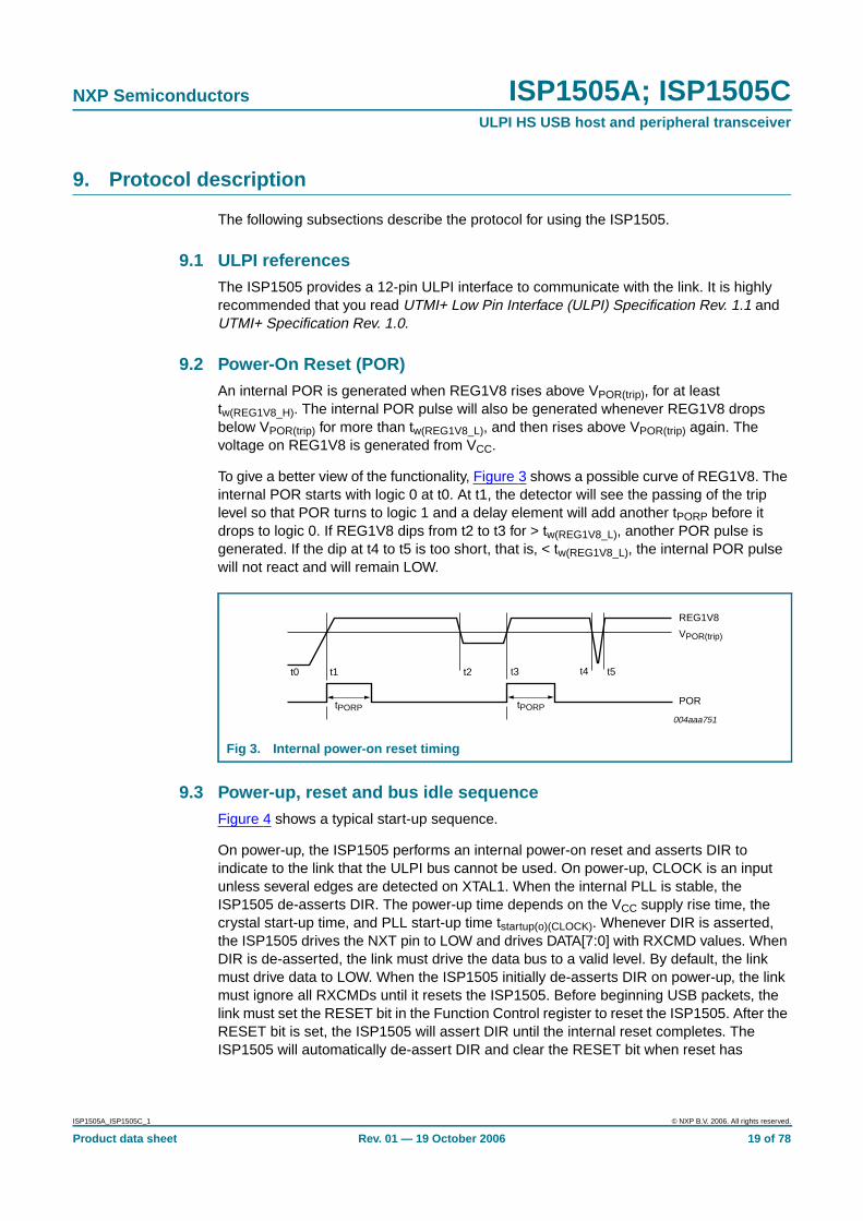
9.2 Power-On Reset (POR)An internal POR is generated when REG1V8 rises above VPOR(trip), for at leasttw(REG1V8_H). The internal POR pulse will also be generated whenever REG1V8 dropsbelow VPOR(trip) for more than tw(REG1V8_L), and then rises above VPOR(trip) again. Thevoltage on REG1V8 is generated from VCC.
To give a better view of the functionality, Figure 3 shows a possible curve of REG1V8. Theinternal POR starts with logic 0 at t0. At t1, the detector will see the passing of the triplevel so that POR turns to logic 1 and a delay element will add another tPORP before itdrops to logic 0. If REG1V8 dips from t2 to t3 for > tw(REG1V8_L), another POR pulse isgenerated. If the dip at t4 to t5 is too short, that is, < tw(REG1V8_L), the internal POR pulsewill not react and will remain LOW.
9.3 Power-up, reset and bus idle sequenceFigure 4 shows a typical start-up sequence.
On power-up, the ISP1505 performs an internal power-on reset and asserts DIR toindicate to the link that the ULPI bus cannot be used. On power-up, CLOCK is an inputunless several edges are detected on XTAL1. When the internal PLL is stable, theISP1505 de-asserts DIR. The power-up time depends on the VCC supply rise time, thecrystal start-up time, and PLL start-up time tstartup(o)(CLOCK). Whenever DIR is asserted,the ISP1505 drives the NXT pin to LOW and drives DATA[7:0] with RXCMD values. WhenDIR is de-asserted, the link must drive the data bus to a valid level. By default, the linkmust drive data to LOW. When the ISP1505 initially de-asserts DIR on power-up, the linkmust ignore all RXCMDs until it resets the ISP1505. Before beginning USB packets, thelink must set the RESET bit in the Function Control register to reset the ISP1505. After theRESET bit is set, the ISP1505 will assert DIR until the internal reset completes. TheISP1505 will automatically de-assert DIR and clear the RESET bit when reset has
Fig 3. Internal power-on reset timing
004aaa751
REG1V8
t0 t1 t2 t3 t4 t5
VPOR(trip)
tPORPPORtPORP
ISP1505A_ISP1505C_1 © NXP B.V. 2006. All rights reserved.
Product data sheet Rev. 01 — 19 October 2006 19 of 78

NXP Semiconductors ISP1505A; ISP1505CULPI HS USB host and peripheral transceiver
completed. After every reset, an RXCMD is sent to the link to update USB statusinformation. After this sequence, the ULPI bus is ready for use and the link can start USBoperations.
If a crystal is attached or a clock is driven into the XTAL1 pin, the ISP1505 will drive a60 MHz clock out from the CLOCK pin when DIR de-asserts. This is shown as CLOCK(output) in Figure 4. If no crystal is attached and a 60 MHz clock is driven into the CLOCKpin, DIR will de-assert when internal clocks have synchronized. This is shown as CLOCK(input) in Figure 4.
The recommended power-up sequence for the link is as follows:
• The link waits for 1 ms, ignoring all the ULPI pin status.
• The link may start to detect DIR status level. If DIR is detected as LOW for three clockcycles, the link may send a RESET command.
• The ULPI interface is ready for use.
ISP1505A_ISP1505C_1 © NXP B.V. 2006. All rights reserved.
Product data sheet Rev. 01 — 19 October 2006 20 of 78

NXP Semiconductors ISP1505A; ISP1505CULPI HS USB host and peripheral transceiver
t1 = VCC and VCC(I/O) are applied to the ISP1505. The ISP1505 regulator starts to turn on. If the ISP1505 CLOCK pin isconfigured as an input, the VCC(I/O) power must be provided at the same time as the VCC power. If the VCC(I/O) power input isdelayed with respect to VCC, input clock mode stability cannot be guaranteed.
t2 = ULPI pads detect REG1V8 rising above the REG1V8 regulator threshold and are not in 3-state. These pads may driveeither LOW or HIGH. It is recommended that the link ignores the ULPI pins status during tPWRUP.
t3 = The POR threshold is reached and the POR pulse is generated. After the POR pulse, ULPI pins are driven to a definedlevel. DIR is driven to HIGH and the other pins are driven to LOW.
t4 = The 19.2 MHz or 26 MHz input clock starts. This clock may be started any time.
t5 = The internal PLL is stabilized after tstartup(PLL). If the 19.2 MHz or 26 MHz clock is started before POR, the internal PLLwill be stabilized after tstartup(PLL) from POR. The CLOCK pin starts to output 60 MHz. The DIR pin will transition from HIGHto LOW. The DIR pin will remain LOW before the link issues a RESET command to the ISP1505.
t6 = The power-up sequence is completed and the ULPI bus interface is ready for use.
Fig 4. Power-up and reset sequence required before the ULPI bus is ready for use
CLOCK(output)
TXCMD
DIR
DATA[7:0]
STP
NXT
004aaa885
RESET command
internal clocks stable
internal resetRXCMD update
bus idle
D
VCC
VCC(I/O)
REG1V8
internalREG1V8detector
internalPOR
XTAL1(output)
tstartup(PLL)
t1 t2 t3 t4 t5 t6
tPWRUP
CLOCK(input)
XTAL1(input)
ISP1505A_ISP1505C_1 © NXP B.V. 2006. All rights reserved.
Product data sheet Rev. 01 — 19 October 2006 21 of 78

NXP Semiconductors ISP1505A; ISP1505CULPI HS USB host and peripheral transceiver
9.3.1 Interface protection
By default, the ISP1505 enables a weak pull-up resistor on STP. If the STP pin isunexpectedly HIGH at any time, the ISP1505 will protect the ULPI interface by enablingweak pull-down resistors on DATA[7:0].
The interface protect feature prevents unwanted activity of the ISP1505 whenever theULPI interface is not correctly driven by the link. For example, when the link powers upmore slowly than the ISP1505.
The interface protect feature can be disabled by setting the INTF_PROT_DIS bit to logic 1.
9.3.2 Interface behavior with respect to RESET_N
The use of the RESET_N pin is optional. When RESET_N is asserted (LOW), theISP1505 will assert DIR. All logic in the ISP1505 will be reset, including the analogcircuitry and ULPI registers. During reset, the link must drive DATA[7:0] and STP to LOW;otherwise undefined behavior may result. When RESET_N is de-asserted (HIGH), theDIR output will de-assert (LOW) four or five clock cycles later. Figure 5 shows the ULPIinterface behavior when RESET_N is asserted (LOW), and when RESET_N issubsequently de-asserted (HIGH). If RESET_N is not used, it must be tied to VCC(I/O).
9.4 VBUS power and fault detection
9.4.1 Driving 5 V on V BUS
The ISP1505 supports external 5 V supplies. The ISP1505 can control the external supplyusing the active-LOW PSW_N open-drain output pin. To enable the external supply bydriving PSW_N to LOW, the link must set the DRV_VBUS_EXT bit in the OTG Controlregister to logic 1. When the DRV_VBUS_EXT bit is set, the DRV_VBUS bit can be set toany value and will be ignored.
Fig 5. Interface behavior with respect to RESET_N
CLOCK
004aaa720
STP
RESET_N
DATA[7:0]
DIR
NXT
Hi-Z (input)
Hi-Z (input)
Hi-Z (input)
Hi-Z (input)
Hi-Z (link must drive)
Hi-Z (link must drive)
ISP1505A_ISP1505C_1 © NXP B.V. 2006. All rights reserved.
Product data sheet Rev. 01 — 19 October 2006 22 of 78

NXP Semiconductors ISP1505A; ISP1505CULPI HS USB host and peripheral transceiver
9.4.2 Fault detection
The ISP1505 supports external VBUS fault detector circuits. An overcurrent detectioncircuit is required for host applications that supply more than 100 mA on VBUS for voltagesbetween 4.75 V to 5.25 V. For low-power applications supplying less than 100 mA, theVBUS power line can directly be connected to the VBUS pin on the ISP1505 and the link canutilize the internal A_VBUS_VLD comparator.
The ISP1505 supports external VBUS fault detector circuits that output a digital faultindicator signal. The indicator signal must be connected to the VBUS/FAULT pin. To enablethe ISP1505 to monitor the digital overcurrent input, the link must set theUSE_EXT_VBUS_IND bit in the OTG Control register. By default, the digital indicator isinterpreted by the ISP1505 as active LOW. That is, a LOW value on VBUS/FAULT indicatesa fault condition has been detected. If the external fault detector provides an active HIGHdigital indicator, the link must set the IND_COMPL bit in the Interface Control register tologic 1. The IND_PASSTHRU bit must be set to logic 1.
By default, the ISP1505 will qualify the external FAULT input with the internal VBUS validcomparator. This can be disabled by setting the IND_PASSTHRU bit to logic 0.
9.5 TXCMD and RXCMDCommands between the ISP1505 and the link are described in the following subsections.
9.5.1 TXCMD
By default, the link must drive the ULPI bus to its idle state of 00h. To send commands andUSB packets, the link drives a nonzero value on DATA[7:0] to the ISP1505 by sending abyte called TXCMD. Commands include USB packet transmissions, and register readsand writes. Once the TXCMD is interpreted and accepted by the ISP1505, the NXT signalis asserted and the link can follow up with the required number of data bytes. The TXCMDbyte format is given in Table 8. Any values other than those in Table 8 are illegal and mayresult in undefined behavior.
Various TXCMD packet and register sequences are shown in later sections.
Table 8. TXCMD byte format
Commandtype name
Command codeDATA[7:6]
Commandpayload DATA[5:0]
Commandname
Command description
Idle 00b 00 0000b NOOP No operation. 00h is the idle value of the data bus. Thelink must drive NOOP by default.
Packettransmit
01b 00 0000b NOPID Transmit USB data that does not have a PID, such aschirp and resume signaling. The ISP1505 startstransmitting only after accepting the next data byte.
00 XXXXb PID Transmit USB packet. DATA[3:0] indicates USB packetidentifier PID[3:0].
ISP1505A_ISP1505C_1 © NXP B.V. 2006. All rights reserved.
Product data sheet Rev. 01 — 19 October 2006 23 of 78
NXP Semiconductors ISP1505A; ISP1505CULPI HS USB host and peripheral transceiver
9.5.2 RXCMD
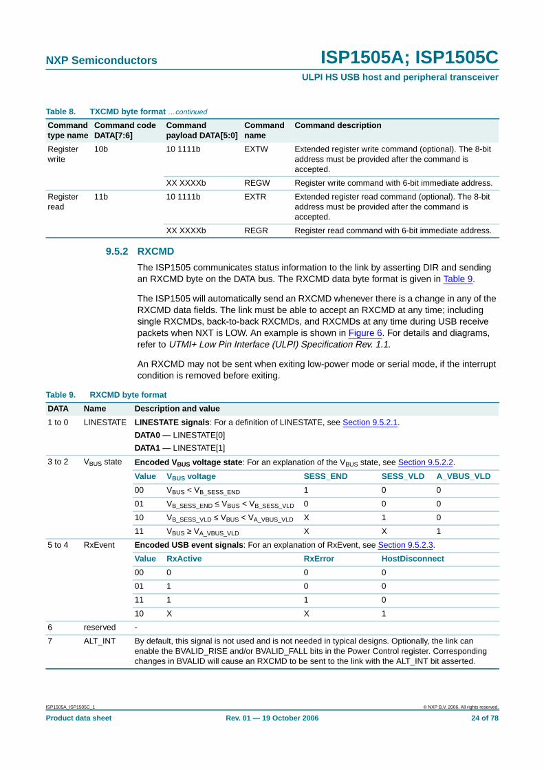
The ISP1505 communicates status information to the link by asserting DIR and sendingan RXCMD byte on the DATA bus. The RXCMD data byte format is given in Table 9.
The ISP1505 will automatically send an RXCMD whenever there is a change in any of theRXCMD data fields. The link must be able to accept an RXCMD at any time; includingsingle RXCMDs, back-to-back RXCMDs, and RXCMDs at any time during USB receivepackets when NXT is LOW. An example is shown in Figure 6. For details and diagrams,refer to UTMI+ Low Pin Interface (ULPI) Specification Rev. 1.1.
An RXCMD may not be sent when exiting low-power mode or serial mode, if the interruptcondition is removed before exiting.
Registerwrite
10b 10 1111b EXTW Extended register write command (optional). The 8-bitaddress must be provided after the command isaccepted.
XX XXXXb REGW Register write command with 6-bit immediate address.
Registerread
11b 10 1111b EXTR Extended register read command (optional). The 8-bitaddress must be provided after the command isaccepted.
XX XXXXb REGR Register read command with 6-bit immediate address.
Table 8. TXCMD byte format …continued
Commandtype name
Command codeDATA[7:6]
Commandpayload DATA[5:0]
Commandname
Command description
Table 9. RXCMD byte format
DATA Name Description and value
1 to 0 LINESTATE LINESTATE signals : For a definition of LINESTATE, see Section 9.5.2.1.
DATA0 — LINESTATE[0]
DATA1 — LINESTATE[1]
3 to 2 VBUS state Encoded V BUS voltage state : For an explanation of the VBUS state, see Section 9.5.2.2.
Value VBUS voltage SESS_END SESS_VLD A_VBUS_VLD
00 VBUS < VB_SESS_END 1 0 0
01 VB_SESS_END ≤ VBUS < VB_SESS_VLD 0 0 0
10 VB_SESS_VLD ≤ VBUS < VA_VBUS_VLD X 1 0
11 VBUS ≥ VA_VBUS_VLD X X 1
5 to 4 RxEvent Encoded USB event signals : For an explanation of RxEvent, see Section 9.5.2.3.
Value RxActive RxError HostDisconnect
00 0 0 0
01 1 0 0
11 1 1 0
10 X X 1
6 reserved -
7 ALT_INT By default, this signal is not used and is not needed in typical designs. Optionally, the link canenable the BVALID_RISE and/or BVALID_FALL bits in the Power Control register. Correspondingchanges in BVALID will cause an RXCMD to be sent to the link with the ALT_INT bit asserted.
ISP1505A_ISP1505C_1 © NXP B.V. 2006. All rights reserved.
Product data sheet Rev. 01 — 19 October 2006 24 of 78

NXP Semiconductors ISP1505A; ISP1505CULPI HS USB host and peripheral transceiver
9.5.2.1 Linestate encoding
LINESTATE[1:0] reflects the current state of DP and DM. Whenever the ISP1505 detectsa change in DP or DM, an RXCMD will be sent to the link with the new LINESTATE[1:0]value. The value given on LINESTATE[1:0] depends on the setting of various registers.
Table 10 shows the LINESTATE[1:0] encoding for upstream facing ports, which applies toperipherals. Table 11 shows the LINESTATE[1:0] encoding for downstream facing ports,which applies to Host Controllers. Dual-role devices must choose the correct table,depending on whether it is in peripheral or host mode.
[1] !squelch indicates inactive squelch. !HS_Differential_Receiver_Output indicates inactive HS_Differential_Receiver_Output.
Fig 6. Single and back-to-back RXCMDs from the ISP1505 to the link
CLOCK
RXCMDDATA[7:0] RXCMD RXCMD
004aaa695
DIR
STP
NXT
Single RXCMD Back-to-back RXCMDs
turnaround turnaround turnaround turnaround
Table 10. LINESTATE[1:0] encoding for upstream facing ports: peripheralsDP_PULLDOWN = 0.[1]
Mode Full-speed High-speed Chirp
XCVRSELECT[1:0] 01, 11 00 00
TERMSELECT 1 0 1
LINESTATE[1:0] 00 SE0 squelch squelch
01 FS-J !squelch !squelch and HS_Differential_Receiver_Output
10 FS-K invalid !squelch and !HS_Differential_Receiver_Output
11 SE1 invalid invalid
ISP1505A_ISP1505C_1 © NXP B.V. 2006. All rights reserved.
Product data sheet Rev. 01 — 19 October 2006 25 of 78

NXP Semiconductors ISP1505A; ISP1505CULPI HS USB host and peripheral transceiver
[1] !squelch indicates inactive squelch. !HS_Differential_Receiver_Output indicates inactive HS_Differential_Receiver_Output.
9.5.2.2 VBUS state encoding
USB devices must monitor the VBUS voltage for purposes such as overcurrent detection,starting a session and SRP. The VBUS state field in the RXCMD is an encoding of thevoltage level on VBUS.
The A_VBUS_VLD, SESS_VLD and SESS_END indicators in the VBUS state are directlytaken from internal comparators built-in to the ISP1505, and encoded as shown in Table 9.
An RXCMD may not be sent when exiting low-power mode or serial mode, if the interruptcondition is removed before exiting.
Note that VBUS and FAULT share the same pin and cannot be simultaneously used.A_VBUS_VLD and FAULT will be interpreted by the ISP1505 as shown in Figure 7.
A description on how to use and select the VBUS state encoding is given in Section “Usingand selecting the VBUS state encoding”.
Table 11. LINESTATE[1:0] encoding for downstream facing ports: hostDP_PULLDOWN and DM_PULLDOWN = 1.[1]
Mode Low-speed Full-speed High-speed Chirp
XCVRSELECT[1:0] 10 01, 11 00 00
TERMSELECT 1 1 0 0
OPMODE[1:0] X X 00, 01, 11 10
LINESTATE[1:0] 00 SE0 SE0 squelch squelch
01 LS-K FS-J !squelch !squelch and HS_Differential_Receiver_Output
10 LS-J FS-K invalid !squelch and !HS_Differential_Receiver_Output
11 SE1 SE1 invalid invalid
Fig 7. RXCMD A_VBUS_VLD indicator source
004aaa752
VBUS/FAULT(0, X)
IND_COMPL
(1, 1)
USE_EXT_VBUS_IND,IND_PASSTHRU
RXCMD A_VBUS_VLD
A_VBUS_VLD comparator(VBUS < 4.4 V)
internal A_VBUS_VLD
complement output
ISP1505A_ISP1505C_1 © NXP B.V. 2006. All rights reserved.
Product data sheet Rev. 01 — 19 October 2006 26 of 78

NXP Semiconductors ISP1505A; ISP1505CULPI HS USB host and peripheral transceiver
Using and selecting the V BUS state encoding: The VBUS state encoding is shown inTable 9. The ISP1505 will send an RXCMD to the link whenever there is a change in theVBUS state. To receive the VBUS state updates, the link must first enable the correspondinginterrupts in the USB Interrupt Enable Rising Edge and USB Interrupt Enable Falling Edgeregisters.
The link can use the VBUS state to monitor VBUS and take appropriate action. Table 12shows the recommended usage for typical applications.
Standard USB Host Controllers : For standard hosts, the system must be able to provide500 mA on VBUS in the range of 4.75 V to 5.25 V. An external circuit must be used todetect overcurrent conditions. If the external overcurrent detector provides a digital faultsignal, then the fault signal must be connected to the ISP1505 FAULT input pin, and thelink must do the following:
1. If the external overcurrent circuit has an active LOW fault or overcurrent indicator, setthe IND_COMPL bit in the Interface Control register to logic 1.
2. Set the IND_PASSTHRU bit in the Interface Control register to logic 1.
3. Set the USE_EXT_VBUS_IND bit in the OTG Control register to logic 1.
Standard USB Peripheral Controllers : Standard peripherals must be able to detectwhen VBUS is at a sufficient level for operation. SESS_VLD must be enabled to detect thestart and end of USB peripheral operations. Detection of A_VBUS_VLD and SESS_ENDthresholds is not needed for standard peripherals.
OTG devices : The ISP1505 provides partial OTG support. A low-power OTG A-devicethat supplies less than 100 mA on VBUS can connect the VBUS power to the ISP1505 VBUSpin. The internal A_VBUS_VLD comparator can be used. If the OTG A-device providesmore than 100 mA on VBUS, an overcurrent detector must be used and "Standard USBHost Controllers " applies. The OTG A-device also uses SESS_VLD to detect when anOTG A-device is initiating VBUS pulsing SRP.
When an OTG device is configured as an OTG B-device, SESS_VLD must be used todetect when VBUS is at a sufficient level for operation. SESS_END must be used to detectwhen VBUS has dropped to a LOW level, allowing the B-device to safely initiate VBUSpulsing SRP.
9.5.2.3 RxEvent encoding
The RxEvent field of the RXCMD informs the link of information related packets receivedon the USB bus. RxActive and RxError are defined in USB 2.0 Transceiver MacrocellInterface (UTMI) Specification Ver. 1.05. HostDisconnect is defined in UTMI+Specification Rev. 1.0. A short definition is also given in the following subsections.
Table 12. VBUS indicators in RXCMD for typical applications
Application A_VBUS_VLD SESS_VLD SESS_END
Standard host yes no no
Standard peripheral no yes no
OTG A-device yes yes no
OTG B-device no yes yes
ISP1505A_ISP1505C_1 © NXP B.V. 2006. All rights reserved.
Product data sheet Rev. 01 — 19 October 2006 27 of 78

NXP Semiconductors ISP1505A; ISP1505CULPI HS USB host and peripheral transceiver
RxActive: When the ISP1505 has detected a SYNC pattern on the USB bus, it signals anRxActive event to the link. An RxActive event can be communicated using two methods.The first method is for the ISP1505 to simultaneously assert DIR and NXT. The secondmethod is for the ISP1505 to send an RXCMD to the link with the RxActive field inRxEvent bits set to logic 1. The link must be able to detect both methods. RxActive framesthe receive packet from the first byte to the last byte.
The link must assume that RxActive is set to logic 0 when indicated in an RXCMD or whenDIR is de-asserted, whichever occurs first.
The link uses RxActive to time high-speed packets and ensure that bus turnaround timesare met. For more information on the USB packet timing, see Section 9.8.1.
RxError: When the ISP1505 has detected an error while receiving a USB packet, itde-asserts NXT and sends an RXCMD with the RxError field set to logic 1. The receivedpacket is no longer valid and must be dropped by the link.
HostDisconnect: HostDisconnect is encoded into the RxEvent field of the RXCMD.HostDisconnect is valid only when the ISP1505 is configured as a host (bothDP_PULLDOWN and DM_PULLDOWN are set to logic 1), and indicates to the HostController when a peripheral is connected or disconnected. The Host Controller mustenable HostDisconnect by setting the HOST_DISCON_R and HOST_DISCON_F bits inthe USB Interrupt Enable Rising Edge and USB Interrupt Enable Falling Edge registers,respectively. Changes in HostDisconnect will cause the PHY to send an RXCMD to thelink with the updated value.
9.6 Register read and write operationsFigure 8 shows register read and write sequences. The ISP1505 supports immediateaddressing and extended addressing register operations. Extended register addressing isoptional for links. Note that register operations will be aborted if the ISP1505 unexpectedlyasserts DIR during the operation. When a register operation is aborted, the link must retryuntil successful. For more information on register operations, refer to UTMI+ Low PinInterface (ULPI) Specification Rev. 1.1.
ISP1505A_ISP1505C_1 © NXP B.V. 2006. All rights reserved.
Product data sheet Rev. 01 — 19 October 2006 28 of 78

NXP Semiconductors ISP1505A; ISP1505CULPI HS USB host and peripheral transceiver
9.7 USB reset and high-speed detection handshake (chirp)Figure 9 shows the sequence of events for USB reset and high-speed detectionhandshake (chirp). The sequence is shown for hosts and peripherals. Figure 9 does notshow all RXCMD updates and timing is not to scale. The sequence is as follows:
1. USB reset: The host detects a peripheral attachment as low-speed if DM is HIGH andas full-speed if DP is HIGH. If a host detects a low-speed peripheral, it does not followthe remainder of this protocol. If a host detects a full-speed peripheral, it resets theperipheral by writing to the Function Control register and settingXCVRSELECT[1:0] = 00b (high-speed) and TERMSELECT = 0b, which drives SE0on the bus (DP and DM connected to ground through 45 Ω). The host also setsOPMODE[1:0] = 10b for correct chirp transmit and receive. The start of SE0 is labeledT0.
Remark: To receive the chirp signaling, the host must also consider the high-speeddifferential receiver output. The Host Controller must interpret LINESTATE[1:0] asshown in Table 11.
2. High-speed detection handshake (chirp)
a. Peripheral chirp: After detecting SE0 for no less than 2.5 µs, if the peripheral iscapable of high-speed, it sets XCVRSELECT[1:0] = 00b (high-speed) andOPMODE[1:0] = 10b (chirp). The peripheral immediately follows this with aTXCMD (NOPID), transmitting a Chirp K for no less than 1 ms and ending no morethan 7 ms after reset time T0. If the peripheral is in low-power mode, it must wakeup its clock within 5.6 ms, leaving 200 µs for the link to start transmitting theChirp K, and 1.2 ms for the Chirp K to complete (worst case with 10 % slow clock).
b. Host chirp: If the host does not detect the peripheral chirp, it must continueasserting SE0 until the end of reset. If the host detects the peripheral Chirp K forno less than 2.5 µs, then no more than 100 µs after the bus leaves the Chirp K
AD indicates the address byte, and D indicates the data byte.
Fig 8. Example of register write, register read, extended register write and extended register read
CLOCK
DIR
DATA[7:0]
NXT
004aaa710
DTXCMD(EXTW) AD D
immediate register write
TXCMD(REGW)
TXCMD(REGR) D AD
TXCMD(EXTW) D
STP
extendedregister write
immediate register read
extendedregister read
ISP1505A_ISP1505C_1 © NXP B.V. 2006. All rights reserved.
Product data sheet Rev. 01 — 19 October 2006 29 of 78

NXP Semiconductors ISP1505A; ISP1505CULPI HS USB host and peripheral transceiver
state, the host sends a TXCMD (NOPID) with an alternating sequence of Chirp Ksand Js. Each Chirp K or Chirp J must last for no less than 40 µs and no longer than60 µs.
c. High-speed idle: The peripheral must detect a minimum of Chirp K-J-K-J-K-J. EachChirp K and Chirp J must be detected for at least 2.5 µs. After seeing thatminimum sequence, the peripheral sets TERMSELECT = 0b andOPMODE[1:0] = 00b. The peripheral is now in high-speed mode and sees !squelch(01b on LINESTATE). When the peripheral sees squelch (10b on LINESTATE), itknows that the host has completed chirp and waits for the high-speed USB trafficto begin. After transmitting the chirp sequence, the host changes OPMODE[1:0] to00b and begins sending USB packets.
For more information, refer to UTMI+ Low Pin Interface (ULPI) Specification Rev. 1.1.
ISP1505A_ISP1505C_1 © NXP B.V. 2006. All rights reserved.
Product data sheet Rev. 01 — 19 October 2006 30 of 78

NXP Semiconductors ISP1505A; ISP1505CULPI HS USB host and peripheral transceiver
Timing is not to scale.
Fig 9. USB reset and high-speed detection handshake (chirp) sequence
004aaa711
KDATA
[7:0]
K JTXCMDNOPID J ...
TXCMD(REGW)
TXCMD(REGW) SE0 K
DIR
00
STP
NXT
XCVRSELECT
TERMSELECT
01 (FS) 00 (HS)
OPMODE
00 (normal) 01 (chirp) 00 (normal)
LINESTATE
J (01b) SE0 (00b) peripheral chirp K (10b) squelch (00b)host chirp K (10b) or chirp J (01b)squelch
(00b)
ULP
I ho
st
KDATA
[7:0]
KTXCMDNOPID K ...SE0
TXCMD(REGW) 00 K J K J K J
TXCMD(REGW) 00
DIR
STP
NXT
XCVRSELECT
01 (FS) 00 (HS)
TERMSELECT
OPMODE
00 (normal) 10 (chirp) 00 (normal)
LINESTATE
J (01b) SE0 (00b) peripheral chirp K (10b)!squelch
(01b)host chirp K or J (10b or 01b)squelch
(00b) squelch (00b)
DP
DM
ULP
I per
iphe
ral
US
B s
igna
ls
USB reset high-speed detection handshake (chirp)
peripheral chirp host chirp HS idleT0
RXCMDs
ISP1505A_ISP1505C_1 © NXP B.V. 2006. All rights reserved.
Product data sheet Rev. 01 — 19 October 2006 31 of 78

NXP Semiconductors ISP1505A; ISP1505CULPI HS USB host and peripheral transceiver
9.8 USB packet transmit and receiveAn example of a packet transmit and receive is shown in Figure 10. For details on USBpackets, refer to UTMI+ Low Pin Interface (ULPI) Specification Rev. 1.1.
9.8.1 USB packet timing
9.8.1.1 ISP1505 pipeline delays
The ISP1505 delays are shown in Table 13. For a detailed description, refer to UTMI+ LowPin Interface (ULPI) Specification Rev. 1.1, Section 3.8.2.6.2.
9.8.1.2 Allowed link decision time
The amount of clock cycles allocated to the link to respond to a received packet andcorrectly receive back-to-back packets is given in Table 14. Link designs must followvalues given in Table 14 for correct USB system operation. Examples of high-speedpacket sequences and timing are shown in Figure 11 and Figure 12. For details, refer toUTMI+ Low Pin Interface (ULPI) Specification Rev. 1.1, Section 3.8.2.6.3.
Fig 10. Example of using the ISP1505 to transmit and receive USB data
CLOCK
TXCMD DATADATA[7:0] turnaround RXCMD DATA turnaround
DIR
STP
NXT
004aaa705
link sendsTXCMD
ISP1505 acceptsTXCMD
link sendsthe next data;
ISP1505 accepts
link signalsend of data
ULPI busis idle
ISP1505asserts DIR,
causingturnaround
cycle
ISP1505 sends
RXCMD(NXT LOW)
ISP1505 sends
USB data(NXT HIGH)
ISP1505deasserts
DIR, causingturnaround
cycle
Table 13. PHY pipeline delays
Parameter name High-speed PHY delay Full-speed PHY delay Low-speed PHY delay
RXCMD delay (J and K) 4 4 4
RXCMD delay (SE0) 4 4 to 6 16 to 18
TX start delay 1 to 2 6 to 10 74 to 75
TX end delay (packets) 3 to 4 not applicable not applicable
TX end delay (SOF) 6 to 9 not applicable not applicable
RX start delay 5 to 6 not applicable not applicable
RX end delay 5 to 6 17 to 18 122 to 123
ISP1505A_ISP1505C_1 © NXP B.V. 2006. All rights reserved.
Product data sheet Rev. 01 — 19 October 2006 32 of 78

NXP Semiconductors ISP1505A; ISP1505CULPI HS USB host and peripheral transceiver
Table 14. Link decision times
Packet sequence High-speedlink delay
Full-speedlink delay
Low-speedlink delay
Definition
Transmit-Transmit(host only)
15 to 24 7 to 18 77 to 247 Number of clocks a host link must wait before driving theTXCMD for the second packet.
In high-speed, the link starts counting from the assertion ofSTP for the first packet.
In full-speed, the link starts counting from the RXCMD,indicating LINESTATE has changed from SE0 to J for thefirst packet. The timing given ensures inter-packet delays of2 bit times to 6.5 bit times.
Receive-Transmit(host orperipheral)
1 to 14 7 to 18 77 to 247 Number of clocks the link must wait before driving theTXCMD for the transmit packet.
In high-speed, the link starts counting from the end of thereceive packet; de-assertion of DIR or an RXCMD,indicating RxActive is LOW.
In full-speed or low-speed, the link starts counting from theRXCMD, indicating LINESTATE has changed from SE0 to Jfor the receive packet. The timing given ensuresinter-packet delays of 2 bit times to 6.5 bit times.
Receive-Receive(peripheral only)
1 1 1 Minimum number of clocks between consecutive receivepackets. The link must be able to receive both packets.
Transmit-Receive(host orperipheral)
92 80 718 Host or peripheral transmits a packet and will time-out afterthis amount of clock cycles if a response is not received.Any subsequent transmission can occur after this time.
Fig 11. High-speed transmit-to-transmit packet timing
004aaa712
DP orDM
DATA EOP IDLE SYNC
CLOCK
DN−1 DNDATA
[7:0]
D0TXCMD D1
DIR
STP
NXT
TX end delay (two to five clocks)
link decision time (15 to 24 clocks)TX start delay
(one to two clocks)
USB interpacket delay (88 to 192 high-speed bit times)
ISP1505A_ISP1505C_1 © NXP B.V. 2006. All rights reserved.
Product data sheet Rev. 01 — 19 October 2006 33 of 78

NXP Semiconductors ISP1505A; ISP1505CULPI HS USB host and peripheral transceiver
9.9 PreamblePreamble packets are headers to low-speed packets that must travel over a full-speedbus, between a host and a hub. To enter preamble mode, the link setsXCVRSELECT[1:0] = 11b in the Function Control register. When in preamble mode, theISP1505 operates just as in full-speed mode, and sends all data with the full-speed riseand fall times. Whenever the link transmits a USB packet in preamble mode, the ISP1505will automatically send a preamble header at full-speed bit rate before sending the linkpacket at low-speed bit rate. The ISP1505 will ensure a minimum gap of four full-speed bittimes between the last bit of the full-speed PRE PID and the first bit of the low-speedpacket SYNC. The ISP1505 will drive a J for at least one full-speed bit time after sendingthe PRE PID, after which the pull-up resistor can hold the J state on the bus. An exampletransmit packet is shown in Figure 13.
In preamble mode, the ISP1505 can also receive low-speed packets from the full-speedbus.
Fig 12. High-speed receive-to-transmit packet timing
004aaa713
DP orDM
DATA EOP IDLE SYNC
CLOCK
DN−4
DN−3
DATA[7:0]
D0TXCMD D1
DIR
STP
NXT
RX end delay (three to eight clocks)
link decision time (1 to 14 clocks)TX start delay
(one to two clocks)
USB interpacket delay (8 to 192 high-speed bit times)
DN−2
DN−1
DN
turnaround
ISP1505A_ISP1505C_1 © NXP B.V. 2006. All rights reserved.
Product data sheet Rev. 01 — 19 October 2006 34 of 78

NXP Semiconductors ISP1505A; ISP1505CULPI HS USB host and peripheral transceiver
9.10 USB suspend and resume
9.10.1 Full-speed and low-speed host-initiated suspend and resume
Figure 14 illustrates how a host or a hub places a full-speed or low-speed peripheral intosuspend and sometime later initiates resume signaling to wake up the downstreamperipheral. Note that Figure 14 timing is not to scale, and does not show all RXCMDLINESTATE updates.
The sequence of events for a host and a peripheral, both with ISP1505, is as follows:
1. Idle: Initially, the host and the peripheral are idle. The host has its 15 kΩ pull-downresistors enabled (DP_PULLDOWN and DM_PULLDOWN are set to 1b) and 45 Ωterminations disabled (TERMSELECT is set to 1b). The peripheral has the 1.5 kΩpull-up resistor connected to DP for full-speed or DM for low-speed (TERMSELECT isset to 1b).
2. Suspend: When the peripheral sees no bus activity for 3 ms, it enters the suspendstate. The peripheral link places the PHY into low-power mode by setting theSUSPENDM bit in the Function Control register, causing the PHY to draw onlysuspend current. The host may or may not be powered down.
3. Resume K: When the host wants to wake up the peripheral, it sets OPMODE[1:0] to10b and transmits a K for at least 20 ms. The peripheral link sees the resume K onLINESTATE, and asserts STP to wake up the PHY.
4. EOP: When STP is asserted, the ISP1505 on the host side automatically appends anEOP of two bits of SE0 at low-speed bit rate, followed by one bit of J. The ISP1505 onthe host side knows to add the EOP because DP_PULLDOWN and DM_PULLDOWNare set to 1b for a host. After the EOP is completed, the host link sets OPMODE[1:0]to 00b for normal operation. The peripheral link sees the EOP and also resumesnormal operation.
DP and DM timing is not to scale.
Fig 13. Preamble sequence
CLOCK
D0TXCMD (low-speed packet ID) D1DATA[7:0]
DIR
STP
NXT
004aaa714
DP or DM FS SYNCFS
PRE IDIDLE (min 4 FS bits)
LS SYNC LS PID LS D0 LS D1
ISP1505A_ISP1505C_1 © NXP B.V. 2006. All rights reserved.
Product data sheet Rev. 01 — 19 October 2006 35 of 78

NXP Semiconductors ISP1505A; ISP1505CULPI HS USB host and peripheral transceiver
9.10.2 High-speed suspend and resume
Figure 15 illustrates how a host or a hub places a high-speed enabled peripheral intosuspend and then initiates resume signaling. The high-speed peripheral will wake up andreturn to high-speed operations. Note that Figure 15 timing is not to scale, and does notshow all RXCMD LINESTATE updates.
Timing is not to scale.
Fig 14. Full-speed suspend and resume
DATA[7:0]
KTXCMDNOPID K ...
TXCMD(REGW)
DIR
STP
NXT
OPMODE 00b 10b 00b
K TXCMD
LINESTATE
J K SE0 J
CLK
DATA[7:0]
TXCMD(REGW) LINESTATE J LINE STATE K SE0 J
DIR
STP
NXT
OPMODE 00b 10b 00b
SUSPENDM
LINESTATE
J K SE0 J
DP
DM
004aaa715
FS
or
LS h
ost (
XC
VR
SE
LEC
T =
01b
(F
S)
or 1
0b (
LS),
DP
PU
LLD
OW
N =
1b,
D
MP
ULL
DO
WN
= 1
b, T
ER
MS
ELE
CT
= 1
b)
FS
or
LS p
erip
hera
l (X
CV
RS
ELE
CT
= 0
1b (
FS
) or
10b
(LS
), D
PP
ULL
DO
WN
= 0
b, T
ER
MS
ELE
CT
= 1
b)U
SB
sig
nals
(onl
y F
S is
sho
wn)
IDLE SUSPEND RESUME K EOP IDLE
ISP1505A_ISP1505C_1 © NXP B.V. 2006. All rights reserved.
Product data sheet Rev. 01 — 19 October 2006 36 of 78

NXP Semiconductors ISP1505A; ISP1505CULPI HS USB host and peripheral transceiver
The sequence of events related to a host and a peripheral, both with ISP1505, is asfollows:
1. High-speed idle: Initially, the host and the peripheral are idle. The host has its 15 kΩpull-down resistors enabled (DP_PULLDOWN and DM_PULLDOWN are set to 1b)and 45 Ω terminations enabled (TERMSELECT is set to 0b). The peripheral has its45 Ω terminations enabled (TERMSELECT is set to 0b).
2. Full-speed suspend: When the peripheral sees no bus activity for 3 ms, it enters thesuspend state. The peripheral link places the ISP1505 into full-speed mode(XCVRSELECT is set to 01b), removes 45 Ω terminations, and enables the 1.5 kΩpull-up resistor on DP (TERMSELECT is set to 1b). The peripheral link then placesthe ISP1505 into low-power mode by setting SUSPENDM, causing the ISP1505 todraw only suspend current. The host also changes the ISP1505 to full-speed(XCVRSELECT is set to 01b), removes 45 Ω terminations (TERMSELECT is set to1b), and then may or may not be powered down.
3. Resume K: When the host wants to wake up the peripheral, it sets OPMODE to 10band transmits a full-speed K for at least 20 ms. The peripheral link sees the resume K(10b) on LINESTATE, and asserts STP to wake up the ISP1505.
4. High-speed traffic: The host link sets high-speed (XCVRSELECT is set to 00b) andenables its 45 Ω terminations (TERMSELECT is set to 0b). The peripheral link seesSE0 on LINESTATE and also sets high-speed (XCVRSELECT is set to 00b), andenables its 45 Ω terminations (TERMSELECT is set to 0b). The host link setsOPMODE to 00b for normal high-speed operation.
ISP1505A_ISP1505C_1 © NXP B.V. 2006. All rights reserved.
Product data sheet Rev. 01 — 19 October 2006 37 of 78

NXP Semiconductors ISP1505A; ISP1505CULPI HS USB host and peripheral transceiver
Timing is not to scale.
Fig 15. High-speed suspend and resume
DATA[7:0]
KTXCMDNOPID K ...
TXCMD(REGW)
DIR
STP
NXT
OPMODE
00b 10b 00b
KTXCMD(REGW)
CLK
DATA[7:0]
TXCMD(REGW) LINESTATE J LINESTATE K SE0
TXCMD(REGW)
DIR
STP
NXT
OPMODE
00b 10b 00b
SUSPENDM
LINESTATE
DP
DM
004aaa717
ULP
I HS
hos
t (D
PP
ULL
DO
WN
= 1
b,D
MP
ULL
DO
WN
= 1
b)U
LPI H
S p
erip
hera
l (D
PP
ULL
DO
WN
= 0
b)U
SB
sig
nals
HS IDLE FS SUSPEND RESUME K
TXCMD(REGW)
HS IDLE
XCVRSELECT
00b 01b 00b
TERMSELECT
LINESTATE
!SQUELCH (01b) FS J (01b)
!SQUELCH (01b)SQUELCH (00b)FS K (10b)
XCVRSELECT
00b 01b 00b
TERMSELECT
!SQUELCH (01b)
SQUELCH (00b) FS J (01b)
!SQUELCH (01b)SQUELCH (00b)FS K (10b)
SQUELCH (00b)
ISP1505A_ISP1505C_1 © NXP B.V. 2006. All rights reserved.
Product data sheet Rev. 01 — 19 October 2006 38 of 78

NXP Semiconductors ISP1505A; ISP1505CULPI HS USB host and peripheral transceiver
9.10.3 Remote wake-up
The ISP1505 supports peripherals that initiate remote wake-up resume. When placed intoUSB suspend, the peripheral link remembers at what speed it was originally operating.Depending on the original speed, the link follows one of the protocols detailed here. InFigure 16, timing is not to scale, and not all RXCMD LINESTATE updates are shown.
The sequence of events related to a host and a peripheral, both with ISP1505, is asfollows:
1. Both the host and the peripheral are assumed to be in low-power mode.
2. The peripheral begins remote wake-up by re-enabling its clock and setting itsSUSPENDM bit to 1b.
3. The peripheral begins driving K on the bus to signal resume. Note that the peripherallink must assume that LINESTATE is K (01b) while transmitting because it will notreceive any RXCMDs.
4. The host recognizes the resume, re-enables its clock and sets its SUSPENDM bit.
5. The host takes over resume driving within 1 ms of detecting the remote wake-up.
6. The peripheral stops driving resume.
7. The peripheral sees the host continuing to drive the resume.
8. The host stops driving resume and the ISP1505 automatically adds the EOP to theend of the resume. The peripheral recognizes the EOP as the end of resume.
9. Both the host and the peripheral revert to normal operation by writing 00b toOPMODE. If the host or the peripheral was previously in high-speed mode, it mustrevert to high-speed before the SE0 of the EOP is completed. This can be achievedby writing XCVRSELECT = 00b and TERMSELECT = 0b after LINESTATE indicatesSE0.
ISP1505A_ISP1505C_1 © NXP B.V. 2006. All rights reserved.
Product data sheet Rev. 01 — 19 October 2006 39 of 78

NXP Semiconductors ISP1505A; ISP1505CULPI HS USB host and peripheral transceiver
9.11 No automatic SYNC and EOP generation (optional)This setting allows the link to turn off the automatic SYNC and EOP generation, and mustbe used for high-speed packets only. It is provided for backward compatibility with legacycontrollers that include SYNC and EOP bytes in the data payload when transmittingpackets. The ISP1505 will not automatically generate the SYNC and EOP patterns whenOPMODE[1:0] is set to 11b. The ISP1505 will still NRZI encode data and perform bitstuffing. An example of a sequence is shown in Figure 17. The link must always sendpackets using the TXCMD (NOPID) type. The ISP1505 does not provide a mechanism tocontrol bit stuffing in individual bytes, but will automatically turn off bit stuffing for EOPwhen STP is asserted with data set to FEh. If data is set to 00h when STP is asserted, the
Timing is not to scale.
Fig 16. Remote wake-up from low-power mode
DATA[7:0]
LINESTATETXCMDREGW
TXCMDREGW00h
TXCMDNOPID
DIR
STP
NXT
XCVRSELECT
01b (FS), 10b (LS) 00b (HS only)
TERMSELECT
OPMODE
10b 00b
DATA[7:0]
LINESTATETXCMDREGW RXCMD00h
TXCMDNOPID RXCMD RXCMD
TXCMDREGW
DIR
STP
NXT
XCVRSELECT
00b (HS), 01b (FS), 10b (LS)
00b (HS only)
TERMSELECT
OPMODE
10b 00b
ULP
I hos
tU
LPI p
erip
hera
l
004aaa718
0b (HS only)
0b (HS only)
ISP1505A_ISP1505C_1 © NXP B.V. 2006. All rights reserved.
Product data sheet Rev. 01 — 19 October 2006 40 of 78

NXP Semiconductors ISP1505A; ISP1505CULPI HS USB host and peripheral transceiver
PHY will not transmit any EOP. The ISP1505 will also detect if the PID byte is A5h,indicating an SOF packet, and automatically send a long EOP when STP is asserted. Totransmit chirp and resume signaling, the link must set OPMODE[1:0] to 10b.
9.12 On-The-Go operationsOn-The-Go (OTG) is a supplement to Universal Serial Bus Specification Rev. 2.0 thatallows a portable USB device to assume the role of a limited USB host by definingimprovements, such as a small connector and low power. Non-portable devices, such asstandard hosts and embedded hosts, can also benefit from OTG features.
The ISP1505 OTG PHY is designed to support all the tasks specified in the OTGsupplement. The ISP1505 provides the front-end analog support for Host NegotiationProtocol (HNP) and Session Request Protocol (SRP) for dual-role devices. Thesupporting components include:
• Voltage comparators
– A_VBUS_VLD
– SESS_VLD (session valid, can be used for both A-session and B-session valid)
– SESS_END (session end)
• Pull-up and pull-down resistors on DP and DM
• Charge and discharge resistors on VBUS
For complete OTG support, the system designer must add a VBUS power supply anddetect the value on the ID pin of the USB cable. This is not provided on the ISP1505.
The following subsections describe how to use the ISP1505 OTG components.
Fig 17. Transmitting USB packets without the automatic SYNC and EOP generation
CLOCK
DATA[7:0]
TXCMD 00h 00h 00h 80h PID D1 D2 D3 ... ...
DN − 1
FEhDN
DIR
STP
NXT
ULP
I sig
nals
TXVALID
TXREADY
TXBITSTUFF
ENABLE
DP,DM
IDLE SYNC PID IDLEEOPDATA PAYLOAD
004aaa719
UT
MI+
equ
ival
ent
sign
als
US
B b
us
ISP1505A_ISP1505C_1 © NXP B.V. 2006. All rights reserved.
Product data sheet Rev. 01 — 19 October 2006 41 of 78

NXP Semiconductors ISP1505A; ISP1505CULPI HS USB host and peripheral transceiver
9.12.1 OTG comparators
The ISP1505 provides comparators that conform to On-The-Go Supplement to theUSB 2.0 Specification Rev. 1.2 requirements of VA_VBUS_VLD, VA_SESS_VLD, VB_SESS_VLDand VB_SESS_END. In this data sheet, VA_SESS_VLD and VB_SESS_VLD are combined intoVB_SESS_VLD. Comparators are described in Section 7.6. Changes in comparator valuesare communicated to the link by RXCMDs as described in Section 9.5.2.2. Control overcomparators is described in Section 10.1.5 to Section 10.1.8.
9.12.2 Pull-up and pull-down resistors
The USB resistors on DP and DM can be used to initiate data-line pulsing SRP. The linkmust set the required bus state using mode settings given in Table 7.
9.12.3 VBUS charge and discharge resistors
A pull-up resistor, RUP(VBUS), is provided to perform VBUS pulsing SRP. A B-device isallowed to charge VBUS above the session valid threshold to request the host to turn onthe VBUS power.
A pull-down resistor, RDN(VBUS), is provided for a B-device to discharge VBUS. This is donewhenever the A-device turns off the VBUS power; the B-device can use the pull-downresistor to ensure VBUS is below VB_SESS_END before starting a session.
For details, refer to On-The-Go Supplement to the USB 2.0 Specification Rev. 1.2.
9.13 Serial modesThe ISP1505 supports both 6-pin serial mode and 3-pin serial mode, controlled bybits 6PIN_FSLS_SERIAL and 3PIN_FSLS_SERIAL of the Interface Control register. Fordetails, refer to UTMI+ Low Pin Interface (ULPI) Specification Rev. 1.1, Section 3.10.
Figure 18 and Figure 19 provide examples of 6-pin serial mode and 3-pin serial mode,respectively.
ISP1505A_ISP1505C_1 © NXP B.V. 2006. All rights reserved.
Product data sheet Rev. 01 — 19 October 2006 42 of 78

NXP Semiconductors ISP1505A; ISP1505CULPI HS USB host and peripheral transceiver
Fig 18. Example of transmit followed by receive in 6-bit serial mode
DATA0(TX_ENABLE)
DATA1(TX_DAT)
DATA2(TX_SE0)
DATA4(RX_DP)
DATA5(RX_DM)
DATA6(RX_RCV)
DP
DM
SYNC DATA EOP
TRANSMIT RECEIVE
SYNC DATA EOP
004aaa692
Fig 19. Example of transmit followed by receive in 3-bit serial mode
DATA0(TX_ENABLE)
DATA1 (TX_DAT/RX_RCV)
DP
DATA2(TX_SE0/RX_SE0)
DM
004aaa693
SYNC DATA EOP
TRANSMIT RECEIVE
SYNC DATA EOP
ISP1505A_ISP1505C_1 © NXP B.V. 2006. All rights reserved.
Product data sheet Rev. 01 — 19 October 2006 43 of 78

NXP Semiconductors ISP1505A; ISP1505CULPI HS USB host and peripheral transceiver
9.14 Aborting transfersThe ISP1505 supports aborting transfers on the ULPI bus. For details, refer to UTMI+ LowPin Interface (ULPI) Specification Rev. 1.1, Section 3.8.4.
9.15 Avoiding contention on the ULPI data busBecause the ULPI data bus is bidirectional, avoid situations in which both the link and thePHY simultaneously drive the data bus.
The following points must be considered while implementing the data bus drive control onthe link.
After power-up and clock stabilization, default states are as follows:
• The ISP1505 drives DIR to LOW.
• The data bus is input to the ISP1505.
• The ULPI link data bus is output, with all data bus lines driven to LOW.
When the ISP1505 wants to take control of the data bus to initiate a data transfer, itchanges the DIR value from LOW to HIGH.
At this point, the link must disable its output buffers. This needs to be as fast as possibleso the link must use a combinational path from DIR.
The ISP1505 will not immediately enable its output buffers, but will delay the enabling ofits buffers until the next clock edge, avoiding bus contention.
When the data transfer is no longer required by the ISP1505, it changes DIR from HIGH toLOW and starts to immediately turn off its output drivers. The link senses the change ofDIR from HIGH to LOW, but delays enabling its output buffers for one CLOCK cycle,avoiding data bus contention.
ISP1505A_ISP1505C_1 © NXP B.V. 2006. All rights reserved.
Product data sheet Rev. 01 — 19 October 2006 44 of 78

NXP Semiconductors ISP1505A; ISP1505CULPI HS USB host and peripheral transceiver
10. Register map
[1] Read (R): A register can be read. Read-only if this is the only mode given.
[2] Write (W): The pattern on the data bus will be written over all bits of a register.
[3] Set (S): The pattern on the data bus is OR-ed with and written to a register.
[4] Clear (C): The pattern on the data bus is a mask. If a bit in the mask is set, then the corresponding register bit will be set to zero(cleared).
10.1 Immediate register set
10.1.1 Vendor ID and Product ID registers
10.1.1.1 Vendor ID Low register
Table 16 shows the bit description of the register.
Table 15. Register map overview
Field name Size(bits
Address (6 bits) References
R[1] W[2] S[3] C[4]
Immediate register set
Vendor ID Low register 8 00h - - - Section 10.1.1 on page 45
Vendor ID High register 8 01h - - -
Product ID Low register 8 02h - - -
Product ID High register 8 03h - - -
Function Control register 8 04h to 06h 04h 05h 06h Section 10.1.2 on page 46
Interface Control register 8 07h to 09h 07h 08h 09h Section 10.1.3 on page 47
OTG Control register 8 0Ah to 0Ch 0Ah 0Bh 0Ch Section 10.1.4 on page 48
USB Interrupt Enable Rising Edgeregister
8 0Dh to 0Fh 0Dh 0Eh 0Fh Section 10.1.5 on page 49
USB Interrupt Enable Falling Edgeregister
8 10h to 12h 10h 11h 12h Section 10.1.6 on page 50
USB Interrupt Status register 8 13h - - - Section 10.1.7 on page 50
USB Interrupt Latch register 8 14h - - - Section 10.1.8 on page 51
Debug register 8 15h - - - Section 10.1.9 on page 51
Scratch register 8 16h to 18h 16h 17h 18h Section 10.1.10 on page 52
Reserved (do not use) - 19h to 2Eh Section 10.1.11 on page 52
Access extended register set 8 - 2Fh - - Section 10.1.12 on page 52
Vendor-specific registers 8 30h to 3Ch Section 10.1.13 on page 52
Power Control register 8 3Dh to 3Fh Section 10.1.14 on page 52
Extended register set Address (8 bits) Section 10.2 on pa ge 53
Maps to immediate register set above 8 00h to 3Fh -
Reserved (do not use) 8 40h to FFh -
Table 16. Vendor ID Low register (address R = 00h) bit description
Bit Symbol Access Value Description
7 to 0 VENDOR_ID_LOW[7:0]
R CCh Vendor ID Low : Lower byte of the NXP vendor ID supplied by USB-IF; hasa fixed value of CCh
ISP1505A_ISP1505C_1 © NXP B.V. 2006. All rights reserved.
Product data sheet Rev. 01 — 19 October 2006 45 of 78

NXP Semiconductors ISP1505A; ISP1505CULPI HS USB host and peripheral transceiver
10.1.1.2 Vendor ID High register
The bit description of the register is given in Table 17.
10.1.1.3 Product ID Low register
The bit description of the Product ID Low register is given in Table 18.
10.1.1.4 Product ID High register
The bit description of the register is given in Table 19.
10.1.2 Function Control register
This register controls UTMI function settings of the PHY. The bit allocation of the registeris given in Table 20.
Table 17. Vendor ID High register (address R = 01h) bit description
Bit Symbol Access Value Description
7 to 0 VENDOR_ID_HIGH[7:0]
R 04h Vendor ID High : Upper byte of the NXP vendor ID supplied by USB-IF;has a fixed value of 04h
Table 18. Product ID Low register (address R = 02h) bit description
Bit Symbol Access Value Description
7 to 0 PRODUCT_ID_LOW[7:0]
R 05h Product ID Low : Lower byte of the NXP product ID number; has a fixedvalue of 05h
Table 19. Product ID High register (address R = 03h) bit description
Bit Symbol Access Value Description
7 to 0 PRODUCT_ID_HIGH[7:0]
R 15h Product ID High : Upper byte of the NXP product ID number; has afixed value of 15h
Table 20. Function Control register (address R = 04h to 06h, W = 04h, S = 05h, C = 06h) bit allocation
Bit 7 6 5 4 3 2 1 0
Symbol reserved SUSPENDM RESET OPMODE[1:0] TERMSELECT
XCVRSELECT[1:0]
Reset 0 1 0 0 0 0 0 1
Access R/W/S/C R/W/S/C R/W/S/C R/W/S/C R/W/S/C R/W/S/C R/W/S/C R/W/S/C
ISP1505A_ISP1505C_1 © NXP B.V. 2006. All rights reserved.
Product data sheet Rev. 01 — 19 October 2006 46 of 78

NXP Semiconductors ISP1505A; ISP1505CULPI HS USB host and peripheral transceiver
10.1.3 Interface Control register
The Interface Control register enables alternative interfaces. All of these modes areoptional features provided for legacy link cores. Setting more than one of these fieldsresults in undefined behavior. Table 22 provides the bit allocation of the register.
Table 21. Function Control register (address R = 04h to 06h, W = 04h, S = 05h, C = 06h) bit description
Bit Symbol Description
7 - reserved
6 SUSPENDM Suspend LOW : Active LOW PHY suspend.
Places the PHY into low-power mode. The PHY will power down all blocks, except thefull-speed receiver, OTG comparators and ULPI interface pins.
To come out of low-power mode, the link must assert STP. The PHY will automatically clearthis bit when it exits low-power mode.
0b — Low-power mode
1b — Powered (default)
5 RESET Reset : Active HIGH transceiver reset.
After the link sets this bit, the PHY will assert DIR and reset the digital core. This does notreset the ULPI interface or the ULPI register set.
When reset is completed, the PHY will de-assert DIR and automatically clear this bit,followed by an RXCMD update to the link.
0b — Do not reset (default)
1b — Reset
The link must wait for DIR to de-assert before using the ULPI bus. Does not reset the ULPIinterface or the ULPI register set.
4 to 3 OPMODE[1:0] Operation Mode : Selects the required bit-encoding style during transmit.
00b — Normal operation (default)
01b — Non-driving
10b — Disable bit-stuffing and NRZI encoding
11b — Do not automatically add SYNC and EOP when transmitting; must be used only forhigh-speed packets
2 TERMSELECT Termination Select : Controls the internal 1.5 kΩ full-speed pull-up resistor and 45 Ωhigh-speed terminations. Control over bus resistors changes, depending onXCVRSELECT[1:0], OPMODE[1:0], DP_PULLDOWN and DM_PULLDOWN, as shown inTable 7.
1 to 0 XCVRSELECT[1:0] Transceiver Select : Selects the required transceiver speed.
00b — Enable the high-speed transceiver
01b — Enable the full-speed transceiver
10b — Enable the low-speed transceiver
11b — Enable the full-speed transceiver for low-speed packets (full-speed preamble isautomatically prefixed)
Table 22. Interface Control register (address R = 07h to 09h, W = 07h, S = 08h, C = 09h) bit allocation
Bit 7 6 5 4 3 2 1 0
Symbol INTF_PROT_DIS
IND_PASSTHRU
IND_COMPL
reserved CLOCK_SUSPENDM
reserved 3PIN_FSLS_SERIAL
6PIN_FSLS_SERIAL
Reset 0 0 0 0 0 0 0 0
Access R/W/S/C R/W/S/C R/W/S/C R/W/S/C R/W/S/C R/W/S/C R/W/S/C R/W/S/C
ISP1505A_ISP1505C_1 © NXP B.V. 2006. All rights reserved.
Product data sheet Rev. 01 — 19 October 2006 47 of 78

NXP Semiconductors ISP1505A; ISP1505CULPI HS USB host and peripheral transceiver
10.1.4 OTG Control register
This register controls various OTG functions of the ISP1505. The bit allocation of the OTGControl register is given in Table 24.
Table 23. Interface Control register (address R = 07h to 09h, W = 07h, S = 08h, C = 09h) bit description
Bit Symbol Description
7 INTF_PROT_DIS Interface Protect Disable : Controls circuitry built into the ISP1505 to protect the ULPIinterface when the link 3-states STP and DATA[7:0]. When this bit is enabled, theISP1505 will automatically detect when the link stops driving STP.
0b — Enables the interface protect circuit (default). The ISP1505 attaches a weakpull-up resistor on STP. If STP is unexpectedly HIGH, the ISP1505 attaches weakpull-down resistors on DATA[7:0], protecting data inputs.
1b — Disables the interface protect circuit, detaches weak pull-down resistors onDATA[7:0], and a weak pull-up resistor on STP.
6 IND_PASSTHRU Indicator Pass-through : The ISP1505 does not support the qualification of an externalFAULT with the internal VA_VBUS_VLD comparator. Either a digital FAULT is input on theVBUS/FAULT pin or the VBUS power is connected to the VBUS/FAULT pin, not both. This bitmust always be set to logic 1.
0b — Not supported.
1b — The complement output signal is not qualified with the internal A_VBUS_VLDcomparator. The link must always set this bit to logic 1.
5 IND_COMPL Indicator Complement : Informs the PHY to invert the FAULT input signal, generatingthe complement output. For details, see Section 9.5.2.2.
0b — The ISP1505 will not invert the FAULT signal (default).
1b — The ISP1505 will invert the FAULT signal.
4 - reserved
3 CLOCK_SUSPENDM Clock Suspend LOW : Active LOW clock suspend.
Powers down the internal clock circuitry only. By default, the clock will not be powered in6-pin serial mode or 3-pin serial mode.
Valid only in 6-pin serial mode and 3-pin serial mode. Valid only when SUSPENDM is setto logic 1, otherwise this bit is ignored.
0b — Clock will not be powered in 3-pin or 6-pin serial mode.
1b — Clock will be powered in 3-pin and 6-pin serial modes.
2 - reserved
1 3PIN_FSLS_SERIAL 3-Pin Full-Speed Low-Speed Serial Mode : Changes the ULPI interface to a 3-bit serialinterface. The PHY will automatically clear this bit when 3-pin serial mode is exited.
0b — Full-speed or low-speed packets are sent using the parallel interface.
1b — Full-speed or low-speed packets are sent using the 3-pin serial interface.
0 6PIN_FSLS_SERIAL 6-Pin Full-Speed Low-Speed Serial Mode : Changes the ULPI interface to a 6-bit serialinterface. The PHY will automatically clear this bit when 6-pin serial mode is exited.
0b — Full-speed or low-speed packets are sent using the parallel interface.
1b — Full-speed or low-speed packets are sent using the 6-pin serial interface.
Table 24. OTG Control register (address R = 0Ah to 0Ch, W = 0Ah, S = 0Bh, C = 0Ch) bit allocation
Bit 7 6 5 4 3 2 1 0
Symbol USE_EXT_VBUS_IND
DRV_VBUS_EXT
DRV_VBUS
CHRG_VBUS
DISCHRG_VBUS
DM_PULLDOWN
DP_PULLDOWN
reserved
Reset 0 0 0 0 0 1 1 0
Access R/W/S/C R/W/S/C R/W/S/C R/W/S/C R/W/S/C R/W/S/C R/W/S/C R/W/S/C
ISP1505A_ISP1505C_1 © NXP B.V. 2006. All rights reserved.
Product data sheet Rev. 01 — 19 October 2006 48 of 78

NXP Semiconductors ISP1505A; ISP1505CULPI HS USB host and peripheral transceiver
10.1.5 USB Interrupt Enable Rising Edge register
The bits in this register enable interrupts and RXCMDs to be sent when the correspondingbits in the USB Interrupt Status register change from logic 0 to logic 1. By default, alltransitions are enabled. Table 26 shows the bit allocation of the register.
Table 25. OTG Control register (address R = 0Ah to 0Ch, W = 0Ah, S = 0Bh, C = 0Ch) bit description
Bit Symbol Description
7 USE_EXT_VBUS_IND
Use External V BUS Indicator : Informs the PHY to use an external VBUS overcurrent indicator.
0b — Use the internal OTG comparator.
1b — Use the external VBUS valid indicator signal input from the FAULT pin.
6 DRV_VBUS_EXT Drive V BUS External : Controls the external VBUS supply through the RESET_N/PSW_N pin.
0b — Do not drive PSW_N to LOW, disabling VBUS.
1b — Drive PSW_N to LOW, enabling VBUS.
5 DRV_VBUS Drive V BUS: Signals the ISP1505 to drive 5 V on VBUS. If DRV_VBUS_EXT is set to logic 1,then setting DRV_VBUS is optional.
4 CHRG_VBUS Charge V BUS: Charges VBUS through a resistor. Used for the VBUS pulsing SRP. The link mustfirst check that VBUS is discharged (see the DISCHRG_VBUS bit), and that both the DP andDM data lines have been LOW (SE0) for 2 ms.
0b — Do not charge VBUS
1b — Charge VBUS
3 DISCHRG_VBUS Discharge V BUS: Discharges VBUS through a resistor. If the link sets this bit to logic 1, it waitsfor an RXCMD indicating that SESS_END has changed from 0 to 1, and then resets this bit to 0to stop the discharge.
0b — Do not discharge VBUS
1b — Discharge VBUS
2 DM_PULLDOWN DM Pull Down : Enables the 15 kΩ pull-down resistor on DM.
0b — Pull-down resistor is not connected to DM.
1b — Pull-down resistor is connected to DM.
1 DP_PULLDOWN DP Pull Down : Enables the 15 kΩ pull-down resistor on DP.
0b — Pull-down resistor is not connected to DP.
1b — Pull-down resistor is connected to DP.
0 - reserved; writing logic 1 will give undefined results
Table 26. USB Interrupt Enable Rising Edge register (address R = 0Dh to 0Fh, W = 0Dh, S = 0Eh, C = 0Fh) bitallocation
Bit 7 6 5 4 3 2 1 0
Symbol reserved SESS_END_R
SESS_VALID_R
VBUS_VALID_R
HOST_DISCON_R
Reset 0 0 0 1 1 1 1 1
Access R/W/S/C R/W/S/C R/W/S/C R/W/S/C R/W/S/C R/W/S/C R/W/S/C R/W/S/C
ISP1505A_ISP1505C_1 © NXP B.V. 2006. All rights reserved.
Product data sheet Rev. 01 — 19 October 2006 49 of 78

NXP Semiconductors ISP1505A; ISP1505CULPI HS USB host and peripheral transceiver
10.1.6 USB Interrupt Enable Falling Edge register
The bits in this register enable interrupts and RXCMDs to be sent when the correspondingbits in the USB Interrupt Status register change from logic 1 to logic 0. By default, alltransitions are enabled. See Table 28.
10.1.7 USB Interrupt Status register
This register (see Table 30) indicates the current value of the interrupt source signal.
Table 27. USB Interrupt Enable Rising Edge register (address R = 0Dh to 0Fh, W = 0Dh, S = 0Eh, C = 0Fh) bitdescription
Bit Symbol Description
7 to 4 - reserved
3 SESS_END_R Session End Rise : Enables interrupts and RXCMDs for logic 0 to logic 1 transitions onSESS_END.
2 SESS_VALID_R Session Valid Rise : Enables interrupts and RXCMDs for logic 0 to logic 1 transitions onSESS_VLD.
1 VBUS_VALID_R VBUS Valid Rise : Enables interrupts and RXCMDs for logic 0 to logic 1 transitions onA_VBUS_VLD.
0 HOST_DISCON_R
Host Disconnect Rise : Enables interrupts and RXCMDs for logic 0 to logic 1 transitions onHOST_DISCON.
Table 28. USB Interrupt Enable Falling Edge register (address R = 10h to 12h, W = 10h, S = 11h, C = 12h) bitallocation
Bit 7 6 5 4 3 2 1 0
Symbol reserved SESS_END_F
SESS_VALID_F
VBUS_VALID_F
HOST_DISCON_F
Reset 0 0 0 1 1 1 1 1
Access R/W/S/C R/W/S/C R/W/S/C R/W/S/C R/W/S/C R/W/S/C R/W/S/C R/W/S/C
Table 29. USB Interrupt Enable Falling Edge register (address R = 10h to 12h, W = 10h, S = 11h, C = 12h) bitdescription
Bit Symbol Description
7 to 4 - reserved
3 SESS_END_F Session End Fall : Enables interrupts and RXCMDs for logic 1 to logic 0 transitions onSESS_END.
2 SESS_VALID_F Session Valid Fall : Enables interrupts and RXCMDs for logic 1 to logic 0 transitions onSESS_VLD.
1 VBUS_VALID_F VBUS Valid Fall : Enables interrupts and RXCMDs for logic 1 to logic 0 transitions onA_VBUS_VLD.
0 HOST_DISCON_F
Host Disconnect Fall : Enables interrupts and RXCMDs for logic 1 to logic 0 transitions onHOST_DISCON.
Table 30. USB Interrupt Status register (address R = 13h) bit allocation
Bit 7 6 5 4 3 2 1 0
Symbol reserved SESS_END
SESS_VALID
VBUS_VALID
HOST_DISCON
Reset X X X 0 0 0 0 0
Access R R R R R R R R
ISP1505A_ISP1505C_1 © NXP B.V. 2006. All rights reserved.
Product data sheet Rev. 01 — 19 October 2006 50 of 78

NXP Semiconductors ISP1505A; ISP1505CULPI HS USB host and peripheral transceiver
10.1.8 USB Interrupt Latch register
The bits of the USB Interrupt Latch register are automatically set by the ISP1505 when anunmasked change occurs on the corresponding interrupt source signal. The ISP1505 willautomatically clear all bits when the link reads this register, or when the PHY enterslow-power mode.
Remark: It is optional for the link to read this register when the clock is running becauseall signal information will automatically be sent to the link through the RXCMD byte.
The bit allocation of this register is given in Table 32.
10.1.9 Debug register
The bit allocation of the Debug register is given in Table 34. This register indicates thecurrent value of signals useful for debugging.
Table 31. USB Interrupt Status register (address R = 13h) bit description
Bit Symbol Description
7 to 4 - reserved
3 SESS_END Session End : Reflects the current value of the session end voltage comparator.
2 SESS_VALID Session Valid : Reflects the current value of the session valid voltage comparator.
1 VBUS_VALID VBUS Valid : Reflects the current value of the VBUS valid voltage comparator.
0 HOST_DISCON Host Disconnect : Reflects the current value of the host disconnect detector.
Table 32. USB Interrupt Latch register (address R = 14h) bit allocation
Bit 7 6 5 4 3 2 1 0
Symbol reserved SESS_END_L
SESS_VALID_L
VBUS_VALID_L
HOST_DISCON_L
Reset 0 0 0 0 0 0 0 0
Access R R R R R R R R
Table 33. USB Interrupt Latch register (address R = 14h) bit description
Bit Symbol Description
7 to 4 - reserved
3 SESS_END_L Session End Latch : Automatically set when an unmasked event occurs on SESS_END.Cleared when this register is read.
2 SESS_VALID_L Session Valid Latch : Automatically set when an unmasked event occurs on SESS_VLD.Cleared when this register is read.
1 VBUS_VALID_L VBUS Valid Latch : Automatically set when an unmasked event occurs on A_VBUS_VLD.Cleared when this register is read.
0 HOST_DISCON_L Host Disconnect Latch : Automatically set when an unmasked event occurs onHOST_DISCON. Cleared when this register is read.
Table 34. Debug register (address R = 15h) bit allocation
Bit 7 6 5 4 3 2 1 0
Symbol reserved LINESTATE1
LINESTATE0
Reset 0 0 0 0 0 0 0 0
Access R R R R R R R R
ISP1505A_ISP1505C_1 © NXP B.V. 2006. All rights reserved.
Product data sheet Rev. 01 — 19 October 2006 51 of 78

NXP Semiconductors ISP1505A; ISP1505CULPI HS USB host and peripheral transceiver
10.1.10 Scratch register
Table 36 shows the bit description of the Scratch register. It is an empty register for testingpurposes.
10.1.11 Reserved
Registers 19h to 2Eh are not implemented. Operating on these addresses will have noeffect on the PHY.
10.1.12 Access extended register set
Address 2Fh does not contain register data. Instead it links to the extended register set.The immediate register set maps to the lower end of the extended register set.
10.1.13 Vendor-specific registers
Addresses 30h to 3Fh contains vendor-specific registers.
10.1.14 Power Control register
Table 37 provides the bit allocation of the Power Control register.
Table 35. Debug register (address R = 15h) bit description
Bit Symbol Description
7 to 2 - reserved
1 LINESTATE1 Line State 1 : Contains the current value of LINESTATE 1
0 LINESTATE0 Line State 0 : Contains the current value of LINESTATE 0
Table 36. Scratch register (address R = 16h to 18h, W = 16h, S = 17h, C = 18h) bit description
Bit Symbol Access Value Description
7 to 0 SCRATCH[7:0]
R/W/S/C 00h Scratch : This is an empty register byte for testing purposes. Softwarecan read, write, set and clear this register; and the functionality of thePHY will not be affected.
Table 37. Power Control register (address R = 3Dh to 3Fh, W = 3Dh, S = 3Eh, C = 3Fh) bit allocation
Bit 7 6 5 4 3 2 1 0
Symbol reserved BVALID_FALL
BVALID_RISE
reserved IGNORE_RESET
Reset 0 0 0 0 0 0 0 0
Access R/W/S/C R/W/S/C R/W/S/C R/W/S/C R/W/S/C R/W/S/C R/W/S/C R/W/S/C
ISP1505A_ISP1505C_1 © NXP B.V. 2006. All rights reserved.
Product data sheet Rev. 01 — 19 October 2006 52 of 78

NXP Semiconductors ISP1505A; ISP1505CULPI HS USB host and peripheral transceiver
10.2 Extended register setAddresses 00h to 3Fh of the extended register set directly map to the immediate set. Thismeans a read, write, set or clear operation to these extended addresses will operate onthe immediate register set.
Addresses 40h to FFh are not implemented. Operating on these addresses will have noeffect on the PHY.
Table 38. Power Control register (address R = 3Dh to 3Fh, W = 3Dh, S = 3Eh, C = 3Fh) bit description
Bit Symbol Description
7 to 4 - reserved; the link must never write logic 1 to these bits.
3 BVALID_FALL BVALID Fall : Enables RXCMDs for HIGH-to-LOW transitions on BVALID. When BVALIDchanges from HIGH to LOW, the ISP1505 will send an RXCMD to the link with the ALT_INTbit set to logic 1.
This bit is optional and is not necessary for OTG devices. The session valid comparator mustbe used instead.
2 BVALID_RISE BVALID Rise : Enables RXCMDs for LOW-to-HIGH transitions on BVALID. When BVALIDchanges from LOW to HIGH, the ISP1505 will send an RXCMD to the link with the ALT_INTbit set to logic 1.
This bit is optional and is not necessary for OTG devices. The session valid comparator mustbe used instead.
1 - reserved
0 IGNORE_RESET Ignore Reset : Selects between the RESET_N and PSW_N functions of theRESET_N/PSW_N pin. The link must set this bit to logic 1, if PSW_N is used in a gangedmode configuration.
0b — The RESET_N/PSW_N pin behaves as an active-LOW reset input (RESET_N). This isthe default setting.
1b — The RESET_N/PSW_N pin behaves as an active-LOW power switch output (PSW_N).
ISP1505A_ISP1505C_1 © NXP B.V. 2006. All rights reserved.
Product data sheet Rev. 01 — 19 October 2006 53 of 78

NXP Semiconductors ISP1505A; ISP1505CULPI HS USB host and peripheral transceiver
11. ElectroStatic Discharge (ESD)
11.1 ESD protectionThe pins that are connected to the USB connector (DP, DM, VBUS and GND) have aminimum of ±4 kV ESD protection. Capacitors 0.1 µF and 1 µF must be connected inparallel from VBUS to GND to achieve this ±4 kV ESD protection (see Figure 20).
Remark: Capacitors 0.1 µF and 1 µF are also required by Universal Serial BusSpecification Rev. 2.0. For details on the requirements for CVBUS, see Section 16.
11.2 ESD test conditionsA detailed report on test setup and results is available on request.
Fig 20. Human body ESD test model
RD1500 Ω
RC1 MΩ
HIGH VOLTAGEDC SOURCE
0.1 µF 1 µF
VBUS
DEVICE UNDER TEST
CS100 pF
storagecapacitor
charge currentlimit resistor
dischargeresistance
GND
A
B
004aaa881
ISP1505A_ISP1505C_1 © NXP B.V. 2006. All rights reserved.
Product data sheet Rev. 01 — 19 October 2006 54 of 78

NXP Semiconductors ISP1505A; ISP1505CULPI HS USB host and peripheral transceiver
12. Limiting values
[1] Equivalent to discharging a 100 pF capacitor through a 1.5 kΩ resistor (Human Body Model JESD22-A114D).
13. Recommended operating conditions
[1] VCC(I/O) should be less than or equal to VCC.
Table 39. Limiting valuesIn accordance with the Absolute Maximum Rating System (IEC 60134).
Symbol Parameter Conditions Min Max Unit
VCC supply voltage −0.5 +4.6 V
VCC(I/O) input/output supply voltage −0.5 +4.6 V
VI input voltage on pins CLOCK, STP, DATA[7:0] andRESET_N/PSW_N
−0.5 VCC(I/O) + 0.5 V V
on pin VBUS/FAULT −0.5 +6.0 V
on pin XTAL1 −0.5 +2.5 V
VESD electrostatic dischargevoltage
on pins DP, DM, VBUS and GND;ILI < 1 µA
[1] −4 +4 kV
on all other pins; ILI < 1 µA −2 +2 kV
Ilu latch-up current −100 +100 mA
Vlu latch-up voltage - 4.6 V
Tstg storage temperature −40 +125 °C
Tj junction temperature −40 +125 °C
Table 40. Recommended operating conditions
Symbol Parameter Conditions Min Typ Max Unit
VCC supply voltage 3.0 3.3 3.6 V
VCC(I/O) input/output supply voltage [1] 1.65 - 3.6 V
VI input voltage on pins CLOCK, STP, DATA[7:0]and RESET_N/PSW_N
0 - VCC(I/O) V
on pin VBUS/FAULT 0 - 5.5 V
on pins DP and DM 0 - 3.6 V
on pin XTAL1 0 - 1.95 V
Tamb ambient temperature −40 +25 +85 °C
ISP1505A_ISP1505C_1 © NXP B.V. 2006. All rights reserved.
Product data sheet Rev. 01 — 19 October 2006 55 of 78

NXP Semiconductors ISP1505A; ISP1505CULPI HS USB host and peripheral transceiver
14. Static characteristics
[1] A continuous stream of 1 kB packets with minimum inter-packet gap and all data bits set to logic 0 for continuous toggling.
Table 41. Static characteristics: supply pinsVCC = 3.0 V to 3.6 V; VCC(I/O) = 1.65 V to 3.6 V; Tamb = −40 °C to +85 °C; unless otherwise specified.Typical values are at VCC = 3.3 V; VCC(I/O) = 3.3 V; Tamb = +25 °C; unless otherwise specified.
Symbol Parameter Conditions Min Typ Max Unit
V(REG3V3) voltage on pin REG3V3 3.0 3.3 3.6 V
V(REG1V8) voltage on pin REG1V8 1.65 1.8 1.95 V
VPOR(trip) power-on reset tripvoltage
1.0 - 1.5 V
ICC supply current low-power mode; VBUS valid detectordisabled; 1.5 kΩ pull-up resistor onpin DP disconnected
- 30 85 µA
low-power mode; VBUS valid detectordisabled; 1.5 kΩ pull-up resistor onpin DP connected
- 215 280 µA
full-speed idle; no USB activity - 10 - mA
high-speed idle; no USB activity - 19 - mA
full-speed continuous data transmit;50 pF load on pins DP and DM
[1] - 15 - mA
full-speed continuous data receive [1] - 11 - mA
high-speed continuous data transmit;45 Ω load on pins DP and DM to ground
[1] - 48 - mA
high-speed continuous data receive [1] - 28 - mA
ICC(I/O) supply current onpin VCC(I/O)
static current; I/O pins are idle - - 1 µA
Table 42. Static characteristics: digital pins (CLOCK, DIR, STP, NXT, DATA[7:0], RESET_N/PSW_N)VCC = 3.0 V to 3.6 V; VCC(I/O) = 1.65 V to 3.6 V; Tamb = −40 °C to +85 °C; unless otherwise specified.Typical values are at VCC = 3.3 V; VCC(I/O) = 3.3 V; Tamb = +25 °C; unless otherwise specified.
Symbol Parameter Conditions Min Typ Max Unit
Input levels
VIL LOW-level input voltage - - 0.3 × VCC(I/O) V
VIH HIGH-level input voltage 0.7 × VCC(I/O) - - V
IIL LOW-level input current VI = 0 V - - 1 µA
IIH HIGH-level input current VI = VCC(I/O) - - 1 µA
ILI input leakage current −1 +0.1 +1 µA
Output levels
VOL LOW-level output voltage IOL = −2 mA - - 0.4 V
VOH HIGH-level output voltage IOH = +2 mA VCC(I/O) − 0.4 V - - V
IOH HIGH-level output current VO = VCC(I/O) − 0.4 V −4.8 - - mA
IOL LOW-level output current VO = 0.4 V 4.2 - - mA
IOZ off-state output current 0 V < VO < VCC(I/O) - - 1 µA
ISP1505A_ISP1505C_1 © NXP B.V. 2006. All rights reserved.
Product data sheet Rev. 01 — 19 October 2006 56 of 78

NXP Semiconductors ISP1505A; ISP1505CULPI HS USB host and peripheral transceiver
Impedance
ZL load impedance 45 - 65 Ω
Pull-up and pull-down
Ipd pull-down current interface protectenabled; DATA[7:0]pins only; VI = VCC(I/O)
25 50 90 µA
Ipu pull-up current interface protectenabled; STP pin only;VI = 0 V
−30 −50 −80 µA
Capacitance
Cin input capacitance pins STP, RESET_N,CLOCK, DATA[7:0]
- - 3.5 pF
Table 42. Static characteristics: digital pins (CLOCK, DIR, STP, NXT, DATA[7:0], RESET_N/PSW_N) …continuedVCC = 3.0 V to 3.6 V; VCC(I/O) = 1.65 V to 3.6 V; Tamb = −40 °C to +85 °C; unless otherwise specified.Typical values are at VCC = 3.3 V; VCC(I/O) = 3.3 V; Tamb = +25 °C; unless otherwise specified.
Symbol Parameter Conditions Min Typ Max Unit
Table 43. Static characteristics: pin V BUS/FAULTVCC = 3.0 V to 3.6 V; VCC(I/O) = 1.65 V to 3.6 V; Tamb = −40 °C to +85 °C; unless otherwise specified.Typical values are at VCC = 3.3 V; VCC(I/O) = 3.3 V; Tamb = +25 °C; unless otherwise specified.Applicable only when pin VBUS/FAULT is used as FAULT.
Symbol Parameter Conditions Min Typ Max Unit
Input levels
VIL LOW-level input voltage - - 0.8 V
VIH HIGH-level input voltage 2.0 - - V
IIL LOW-level input current VI = 0 V - - 1 µA
IIH HIGH-level input current VI = VCC(I/O) - - 1 µA
Table 44. Static characteristics: analog I/O pins (DP, DM)VCC = 3.0 V to 3.6 V; VCC(I/O) = 1.65 V to 3.6 V; Tamb = −40 °C to +85 °C; unless otherwise specified.Typical values are at VCC = 3.3 V; VCC(I/O) = 3.3 V; Tamb = +25 °C; unless otherwise specified.
Symbol Parameter Conditions Min Typ Max Unit
Original USB transceiver (low-speed and full-speed)
Input levels (differential receiver)
VDI differential input sensitivity |VDP − VDM| 0.2 - - V
VCM differential common mode voltagerange
includes VDI range 0.8 - 2.5 V
Input levels (single-ended receivers)
VIL LOW-level input voltage - - 0.8 V
VIH HIGH-level input voltage 2.0 - - V
Output levels
VOL LOW-level output voltage pull-up on pin DP;RL = 1.5 kΩ to 3.6 V
0.0 0.18 0.3 V
VOH HIGH-level output voltage pull-down on pins DP andDM; RL = 15 kΩ to GND
2.8 3.2 3.6 V
ISP1505A_ISP1505C_1 © NXP B.V. 2006. All rights reserved.
Product data sheet Rev. 01 — 19 October 2006 57 of 78

NXP Semiconductors ISP1505A; ISP1505CULPI HS USB host and peripheral transceiver
[1] For high-speed USB and full-speed USB.
Termination
VTERM termination voltage for 1.5 kΩ pull-up resistor 3.0 - 3.6 V
Resistance
RUP(DP) pull-up resistance on pin DP 1425 1500 1575 Ω
High-speed USB transceiver
Input levels (differential receiver)
VHSSQ high-speed squelch detectionthreshold voltage (differentialsignal amplitude)
100 - 150 mV
VHSDSC high-speed disconnect detectionthreshold voltage (differentialsignal amplitude)
525 - 625 mV
VHSDI high-speed differential inputsensitivity
|VDP − VDM| 300 - - mV
VHSCM high-speed data signalingcommon mode voltage range
includes VDI range −50 - +500 mV
VHSOI high-speed idle level −10 - +10 mV
VHSOL high-speed data signalingLOW-level voltage
−10 - +10 mV
Output levels
VHSOH high-speed data signalingHIGH-level voltage
360 - 440 mV
VCHIRPJ Chirp J level (differential voltage) 700 - 1100 mV
VCHIRPK Chirp K level (differential voltage) −900 - −500 mV
Leakage current
ILZ off-state leakage current −1 - +1 µA
Capacitance
Cin input capacitance pin to GND - - 5 pF
Resistance
RDN(DP) pull-down resistance on pin DP 14.25 15 15.75 kΩ
RDN(DM) pull-down resistance on pin DM 14.25 15 15.75 kΩ
Termination
ZO(drv)(DP) driver output impedance on pin DP steady-state drive [1] 40.5 45 49.5 Ω
ZO(drv)(DM) driver output impedance onpin DM
steady-state drive [1] 40.5 45 49.5 Ω
ZINP input impedance 10 - - MΩ
Table 44. Static characteristics: analog I/O pins (DP, DM) …continuedVCC = 3.0 V to 3.6 V; VCC(I/O) = 1.65 V to 3.6 V; Tamb = −40 °C to +85 °C; unless otherwise specified.Typical values are at VCC = 3.3 V; VCC(I/O) = 3.3 V; Tamb = +25 °C; unless otherwise specified.
Symbol Parameter Conditions Min Typ Max Unit
ISP1505A_ISP1505C_1 © NXP B.V. 2006. All rights reserved.
Product data sheet Rev. 01 — 19 October 2006 58 of 78

NXP Semiconductors ISP1505A; ISP1505CULPI HS USB host and peripheral transceiver
Table 45. Static characteristics: V BUS comparatorsVCC = 3.0 V to 3.6 V; VCC(I/O) = 1.65 V to 3.6 V; Tamb = −40 °C to +85 °C; unless otherwise specified.Typical values are at VCC = 3.3 V; VCC(I/O) = 3.3 V; Tamb = +25 °C; unless otherwise specified.
Symbol Parameter Conditions Min Typ Max Unit
VA_VBUS_VLD A-device VBUS valid voltage 4.4 4.5 4.65 V
VB_SESS_VLD B-device session valid voltage for A-device andB-device
0.8 1.6 2.0 V
Vhys(B_SESS_VLD) B-device session valid hysteresisvoltage
70 140 200 mV
VB_SESS_END B-device session end voltage 0.2 0.5 0.8 V
Table 46. Static characteristics: V BUS resistorsVCC = 3.0 V to 3.6 V; VCC(I/O) = 1.65 V to 3.6 V; Tamb = −40 °C to +85 °C; unless otherwise specified.Typical values are at VCC = 3.3 V; VCC(I/O) = 3.3 V; Tamb = +25 °C; unless otherwise specified.
Symbol Parameter Conditions Min Typ Max Unit
RUP(VBUS) pull-up resistance onpin VBUS
connect to pin REG3V3 whenCHRG_VBUS is logic 1
281 680 - Ω
RDN(VBUS) pull-down resistance onpin VBUS
connect to GND whenDISCHRG_VBUS is logic 1
656 850 - Ω
RI(idle)(VBUS) idle input resistance onpin VBUS
40 57 80 kΩ
Table 47. Static characteristics: resistor referenceVCC = 3.0 V to 3.6 V; VCC(I/O) = 1.65 V to 3.6 V; Tamb = −40 °C to +85 °C; unless otherwise specified.Typical values are at VCC = 3.3 V; VCC(I/O) = 3.3 V; Tamb = +25 °C; unless otherwise specified.
Symbol Parameter Conditions Min Typ Max Unit
VO(RREF) output voltage on pin RREF SUSPENDM is logic 1 - 1.22 - V
ISP1505A_ISP1505C_1 © NXP B.V. 2006. All rights reserved.
Product data sheet Rev. 01 — 19 October 2006 59 of 78

NXP Semiconductors ISP1505A; ISP1505CULPI HS USB host and peripheral transceiver
15. Dynamic characteristics
[1] RMS = Root Mean Square.
Table 48. Dynamic characteristics: reset and clockVCC = 3.0 V to 3.6 V; VCC(I/O) = 1.65 V to 3.6 V; Tamb = −40 °C to +85 °C; unless otherwise specified.Typical values are at VCC = 3.3 V; VCC(I/O) = 3.3 V; Tamb = +25 °C; unless otherwise specified.
Symbol Parameter Conditions Min Typ Max Unit
Reset
tW(POR) internal power-on reset pulsewidth
0.2 - - µs
tw(REG1V8_H) REG1V8 HIGH pulse width 2 - - µs
tw(REG1V8_L) REG1V8 LOW pulse width 11 - - µs
tW(RESET_N) external RESET_N pulse width 200 - - ns
tPWRUP regulator start-up time 4.7 µF ± 20 % capacitoreach on pins REG1V8and REG3V3
- - 1 ms
Crystal or clock applied to XTAL1
fi(XTAL1) input frequency on pin XTAL1 ISP1505ABS - 19.2 - MHz
ISP1505CBS - 26 - MHz
tjit(i)(XTAL1)RMS RMS input jitter on pin XTAL1 ISP1505ABS [1] - - 200 ps
ISP1505CBS [1] - - 300 ps
∆fi(XTAL1) input frequency tolerance onpin XTAL1
- 50 200 ppm
tr(XTAL1) rise time on pin XTAL1 only for square wave input - - 5 ns
tf(XTAL1) fall time on pin XTAL1 only for square wave input - - 5 ns
V(XTAL1)(p-p) peak-to-peak voltage onpin XTAL1
only for square wave input 0.566 - 1.95 V
External clock input on CLOCK
fi(CLOCK) input frequency on pin CLOCK - 60 - MHz
tjit(i)(CLOCK)RMS RMS input jitter on pin CLOCK [1] - - 200 ps
∆fi(CLOCK) input frequency tolerance onpin CLOCK
- 50 200 ppm
δi(CLOCK) input clock duty cycle onpin CLOCK
45 50 55 %
Output CLOCK characteristics
fo(CLOCK) output frequency on pin CLOCK active only when a crystalor clock is input onpin XTAL1
- 60 - MHz
tjit(o)(CLOCK)RMS RMS output jitter on pin CLOCK [1] - - 500 ps
δo(CLOCK) output clock duty cycle onpin CLOCK
45 50 55 %
tstartup(PLL) PLL startup time - 650 - µs
tstartup(o)(CLOCK) output CLOCK start-up time measured from powergood or assertion ofpin STP
450 650 900 µs
ISP1505A_ISP1505C_1 © NXP B.V. 2006. All rights reserved.
Product data sheet Rev. 01 — 19 October 2006 60 of 78

NXP Semiconductors ISP1505A; ISP1505CULPI HS USB host and peripheral transceiver
Table 49. Dynamic characteristics: digital I/O pinsVCC = 3.0 V to 3.6 V; VCC(I/O) = 1.65 V to 3.6 V; Tamb = −40 °C to +85 °C; unless otherwise specified.Typical values are at VCC = 3.3 V; Tamb = +25 °C; unless otherwise specified.
Symbol Parameter Conditions Min Typ Max Unit
Output 60 MHz CLOCK, V CC(I/O) = 1.65 V to 1.95 V
tsu(DATA) DATA set-up time with respect tothe rising edge of pin CLOCK
20 pF total external loadper pin
5.7 - - ns
th(DATA) DATA hold time with respect tothe rising edge of pin CLOCK
20 pF total external loadper pin
0 - - ns
td(DATA) DATA output delay with respectto the rising edge of pin CLOCK
20 pF total external loadper pin
- - 7.8 ns
tsu(STP) STP set-up time with respect tothe rising edge of pin CLOCK
20 pF total external loadper pin
4.5 - - ns
th(STP) STP hold time with respect tothe rising edge of pin CLOCK
20 pF total external loadper pin
0 - - ns
td(DIR) DIR output delay with respect tothe rising edge of pin CLOCK
20 pF total external loadper pin
- - 8.9 ns
td(NXT) NXT output delay with respect tothe rising edge of pin CLOCK
20 pF total external loadper pin
- - 8.9 ns
Output 60 MHz CLOCK, V CC(I/O) = 3.0 V to 3.6 V
tsu(DATA) DATA set-up time with respect tothe rising edge of pin CLOCK
30 pF total external loadper pin
3.3 - - ns
th(DATA) DATA hold time with respect tothe rising edge of pin CLOCK
30 pF total external loadper pin
0.8 - - ns
td(DATA) DATA output delay with respectto the rising edge of pin CLOCK
30 pF total external loadper pin
- - 5.5 ns
tsu(STP) STP set-up time with respect tothe rising edge of pin CLOCK
30 pF total external loadper pin
3.4 - - ns
th(STP) STP hold time with respect tothe rising edge of pin CLOCK
30 pF total external loadper pin
0.8 - - ns
td(DIR) DIR output delay with respect tothe rising edge of pin CLOCK
30 pF total external loadper pin
- - 6.6 ns
td(NXT) NXT output delay with respect tothe rising edge of pin CLOCK
30 pF total external loadper pin
- - 6.6 ns
Input 60 MHz CLOCK, V CC(I/O) = 1.65 V to 1.95 V
tsu(DATA) DATA set-up time with respect tothe rising edge of pin CLOCK
10 pF total external loadper pin
4.9 4.4 - ns
th(DATA) DATA hold time with respect tothe rising edge of pin CLOCK
10 pF total external loadper pin
0 - - ns
td(DATA) DATA output delay with respectto the rising edge of pin CLOCK
10 pF total external loadper pin
9.2 5.2 - ns
tsu(STP) STP set-up time with respect tothe rising edge of pin CLOCK
10 pF total external loadper pin
3.5 3.4 - ns
th(STP) STP hold time with respect tothe rising edge of pin CLOCK
10 pF total external loadper pin
0 - - ns
td(DIR) DIR output delay with respect tothe rising edge of pin CLOCK
10 pF total external loadper pin
- 4.9 9.3 ns
td(NXT) NXT output delay with respect tothe rising edge of pin CLOCK
10 pF total external loadper pin
- 4.9 9.3 ns
ISP1505A_ISP1505C_1 © NXP B.V. 2006. All rights reserved.
Product data sheet Rev. 01 — 19 October 2006 61 of 78

NXP Semiconductors ISP1505A; ISP1505CULPI HS USB host and peripheral transceiver
Input 60 MHz CLOCK, V CC(I/O) = 3.0 V to 3.6 V
tsu(DATA) DATA set-up time with respect tothe rising edge of pin CLOCK
20 pF total external loadper pin
3.4 3.0 - ns
th(DATA) DATA hold time with respect tothe rising edge of pin CLOCK
20 pF total external loadper pin
0 - - ns
td(DATA) DATA output delay with respectto the rising edge of pin CLOCK
20 pF total external loadper pin
7.7 4.1 - ns
tsu(STP) STP set-up time with respect tothe rising edge of pin CLOCK
20 pF total external loadper pin
3.1 2.7 - ns
th(STP) STP hold time with respect tothe rising edge of pin CLOCK
20 pF total external loadper pin
0 - - ns
td(DIR) DIR output delay with respect tothe rising edge of pin CLOCK
20 pF total external loadper pin
7.3 3.8 - ns
td(NXT) NXT output delay with respect tothe rising edge of pin CLOCK
20 pF total external loadper pin
7.3 3.8 - ns
Table 49. Dynamic characteristics: digital I/O pins …continuedVCC = 3.0 V to 3.6 V; VCC(I/O) = 1.65 V to 3.6 V; Tamb = −40 °C to +85 °C; unless otherwise specified.Typical values are at VCC = 3.3 V; Tamb = +25 °C; unless otherwise specified.
Symbol Parameter Conditions Min Typ Max Unit
Table 50. Dynamic characteristics: analog I/O pins (DP, DM)VCC = 3.0 V to 3.6 V; VCC(I/O) = 1.65 V to 3.6 V; Tamb = −40 °C to +85 °C; unless otherwise specified.Typical values are at VCC = 3.3 V; VCC(I/O) = 3.3 V; Tamb = +25 °C; unless otherwise specified.
Symbol Parameter Conditions Min Typ Max Unit
High-speed driver
tHSR rise time (10 % to 90 %) 500 - - ps
tHSF fall time (10 % to 90 %) 500 - - ps
Full-speed driver
tFR rise time CL = 50 pF; 10 % to 90 % of|VOH − VOL|
4 - 20 ns
tFF fall time CL = 50 pF; 10 % to 90 % of|VOH − VOL|
4 - 20 ns
tFRFM differential rise and fall timematching
excluding the first transitionfrom the idle state
90 - 111.1 %
VCRS output signal crossovervoltage
excluding the first transitionfrom the idle state
1.3 - 2.0 V
Low-speed driver
tLR transition time: rise time CL = 200 pF to 600 pF;1.5 kΩ pull-up on DMenabled; 10 % to 90 % of|VOH − VOL|
75 - 300 ns
tLF transition time: fall time CL = 200 pF to 600 pF;1.5 kΩ pull-up on DMenabled; 10 % to 90 % of|VOH − VOL|
75 - 300 ns
tLRFM rise and fall time matching tLR/tLF; excluding the firsttransition from the idle state
80 - 125 %
ISP1505A_ISP1505C_1 © NXP B.V. 2006. All rights reserved.
Product data sheet Rev. 01 — 19 October 2006 62 of 78

NXP Semiconductors ISP1505A; ISP1505CULPI HS USB host and peripheral transceiver
Driver timing
tPLH(drv) driver propagation delay(LOW to HIGH)
TX_DAT, TX_SE0 to DP, DM;see Figure 22
- - 11 ns
tPHL(drv) driver propagation delay(HIGH to LOW)
TX_DAT, TX_SE0 to DP, DM;see Figure 22
- - 11 ns
tPHZ driver disable delay fromHIGH level
TX_ENABLE to DP, DM;see Figure 23
- - 12 ns
tPLZ driver disable delay fromLOW level
TX_ENABLE to DP, DM;see Figure 23
- - 12 ns
tPZH driver enable delay to HIGHlevel
TX_ENABLE to DP, DM;see Figure 23
- - 20 ns
tPZL driver enable delay to LOWlevel
TX_ENABLE to DP, DM;see Figure 23
- - 20 ns
Receiver timing
Differential receiver
tPLH(rcv) receiver propagation delay(LOW to HIGH)
DP, DM to RX_RCV, RX_DPand RX_DM; see Figure 24
- - 17 ns
tPHL(rcv) receiver propagation delay(HIGH to LOW)
DP, DM to RX_RCV, RX_DPand RX_DM; see Figure 24
- - 17 ns
Single-ended receiver
tPLH(se) single-ended propagationdelay (LOW to HIGH)
DP, DM to RX_RCV, RX_DPand RX_DM; see Figure 24
- - 17 ns
tPHL(se) single-ended propagationdelay (HIGH to LOW)
DP, DM to RX_RCV, RX_DPand RX_DM; see Figure 24
- - 17 ns
Table 50. Dynamic characteristics: analog I/O pins (DP, DM) …continuedVCC = 3.0 V to 3.6 V; VCC(I/O) = 1.65 V to 3.6 V; Tamb = −40 °C to +85 °C; unless otherwise specified.Typical values are at VCC = 3.3 V; VCC(I/O) = 3.3 V; Tamb = +25 °C; unless otherwise specified.
Symbol Parameter Conditions Min Typ Max Unit
ISP1505A_ISP1505C_1 © NXP B.V. 2006. All rights reserved.
Product data sheet Rev. 01 — 19 October 2006 63 of 78

NXP Semiconductors ISP1505A; ISP1505CULPI HS USB host and peripheral transceiver
15.1 ULPI timingULPI interface timing requirements are given in Figure 25. This timing applies tosynchronous mode only. All timing is measured with respect to the ISP1505 CLOCK pin.All signals are clocked on the rising edge of CLOCK.
Fig 21. Rise time and fall time Fig 22. Timing of TX_DAT and TX_SE0 to DP and DM
Fig 23. Timing of TX_ENABLE to DP and DM Fig 24. Timing of DP and DM to RX_RCV, RX_DP andRX_DM
004aaa861VOL
tHSR, tFR, tLR tHSF, tFF, tLF
VOH90 %
10 % 10 %
90 %
004aaa573VOL
VOH
tPHL(drv)tPLH(drv)
VCRS VCRS
0.9 V0.9 V
1.8 V
0 V
logic input
differentialdata lines
004aaa574VOL
VOH
tPZHtPZL
tPHZtPLZ
VOH − 0.3 V
VOL + 0.3 V
VCRS
0.9 V0.9 V
1.8 V
0 V
logic input
differentialdata lines
tPLH(se) tPHL(se)
004aaa575VOL
VOH
tPHL(rcv)tPLH(rcv)
VCRS VCRS
0.9 V0.9 V
2.0 V
0.8 V
logic output
differentialdata lines
Fig 25. ULPI timing interface
CLOCK
CONTROL IN(STP)
DATA IN(8-BIT)
tsu(STP) th(STP)
tsu(DATA) th(DATA)
CONTROL OUT(DIR, NXT)
DATA OUT(8-BIT)
004aaa722
td(DIR),td(NXT)
td(DATA)
td(DIR),td(NXT)
ISP1505A_ISP1505C_1 © NXP B.V. 2006. All rights reserved.
Product data sheet Rev. 01 — 19 October 2006 64 of 78

NXP Semiconductors ISP1505A; ISP1505CULPI HS USB host and peripheral transceiver
16. Application information
[1] For detailed information and alternative interface options, refer to the Interfacing to the ISP1504/5/6 (AN10048) application note.
Table 51. Recommended bill of materials
Designator [1] Application Value Comment
Cbypass highly recommended for allapplications
0.1 µF -
Cfilter highly recommended for allapplications
4.7 µF ± 20 %; use a LOWESR capacitor (0.2 Ω to2 Ω) for best performance
-
CVBUS mandatory for peripherals 0.1 µF and 1 µF to 10 µF inparallel
-
mandatory for host 0.1 µF and 120 µF ± 20 %(min) in parallel
-
mandatory for OTG 0.1 µF and 1 µF to 6.5 µFin parallel
-
DESD recommended for allESD-sensitive applications
IP4059CX5/LF Wafer-Level Chip-Scale Package (WLCSP);1.34 mm × 0.96 mm × 0.41 mm; ESDIEC 61000-4-2 level 4; ±8 kV contact; ±15 kVair discharge
Rpullup recommended; for applicationswith an external VBUS supplycontrolled by PSW_N
4.7 kΩ to 100 kΩ (10 kΩrecommended)
maximum value is determined by the voltagedrop on PSW_N caused by leakage intoPSW_N and the external supply control pin
RRREF mandatory in all applications 12 kΩ ± 1 % -
RVBUS strongly recommended forperipheral or external 5 Vapplications only
1 kΩ ± 5 % -
RXTAL required only for applicationsdriving a square wave into theXTAL1 pin
47 kΩ ± 5 % used to avoid floating input on the XTAL1 pin
XTAL crystal is used 19.2 MHz CL = 10 pF; RS < 220 Ω; CXTAL = 18 pF
26 MHz CL = 10 pF; RS < 130 Ω; CXTAL = 18 pF
C(XTAL)SQ required only for applicationsdriving a square wave into theXTAL1 pin that has a DC offset
100 pF used to AC couple the input square wave tothe XTAL1 pin
ISP1505A_ISP1505C_1 © NXP B.V. 2006. All rights reserved.
Product data sheet Rev. 01 — 19 October 2006 65 of 78

xxxxxxxxxxxxxxxxxxxxx xxxxxxxxxxxxxxxxxxxxxxxxxx xxxxxxx x x x xxxxxxxxxxxxxxxxxxxxxxxxxxxxxx xxxxxxxxxxxxxxxxxxx xx xxxxxxx xxxxxxxxxxxxxxxxxxxxxxxxxxx xxxxxxxxxxxxxxxxxxx xxxxxx xxxxxxxxxxxxxxxxxxxxxxxxxxxxxxxxxxx xxxxxxxxxxxx x xxxxxxxxxxxxxxxxxxxxxx xxxxxxxxxxxxxxxxxxxxxxxxxxxxxx xxxxx xxxxxxxxxxxxxxxxxxxxxxxxxxxxxxxxxxxxxxxxxxxxxxxxxx xxxxxxxxxxxxxxxxxxxxxxxxxxxxxxxxx xxxxxxxxxxxxxxxxxxxx xxx
ISP
1505A_IS
P1505C
_1
Product data shee
NX
P S
emiconductors
ISP
1505A; IS
P1505C
ULP
I HS
US
B host and peripheral transceiver
A2
A3
(I/O)
A4
CK
A5
A6
A7
T
1V8
HOSTCONTROLLER
D0
D2
D3
D4
D5
D6
D7
NXT
CLOCK
STP
DIRRESET_N (optional)
D1
004aaa589
Cbypass Cfilter
© N
XP
B.V. 2006. A
ll rights reserved.
tR
ev. 01 — 19 O
ctober 200666 of 78
(1) Frequency is version dependent: ISP1505ABS: 19.2 MHz; ISP1505CBS: 26 MHz.
Fig 26. Using the ISP1505 with a USB Host Controller; external 5 V source with built-in FAULT and external crystal
ISP1505
DATA1
VCC(I/O)
RREF
DM
DP
VCC
DAT
DAT
VCC
DAT
CLO
DAT
DAT
DAT
NX
STP
7
6
5
4
3
1
15
16
17
18
19
21
20
23
22
24
VBUS/FAULT
REG3V3
XTAL1
XTAL2 11
10
9
8
DIR
REGRESET_N/
PSW_N12 13
14
USB STANDARDOR MINI-A
RECEPTACLE
VBUS
D−
D+
GND4
3
2
1
VCC(I/O)VCC
GND (die pad)
2DATA0
XTAL(1)
+5 V
IN FAULT
ON OUT
VBUSSWITCH
RpullupCbypass Cbypass
Cbypass CfilterCVBUS CXTAL CXTAL
RRREF
5
6
7
8
SHIELD
SHIELD
SHIELD
SHIELD
Cbypass
IP4059CX5/LF
B2
C1 A1 A3 C3
DESD
RVBUS

xxxxxxxxxxxxxxxxxxxxx xxxxxxxxxxxxxxxxxxxxxxxxxx xxxxxxx x x x xxxxxxxxxxxxxxxxxxxxxxxxxxxxxx xxxxxxxxxxxxxxxxxxx xx xxxxxxx xxxxxxxxxxxxxxxxxxxxxxxxxxx xxxxxxxxxxxxxxxxxxx xxxxxx xxxxxxxxxxxxxxxxxxxxxxxxxxxxxxxxxxx xxxxxxxxxxxx x xxxxxxxxxxxxxxxxxxxxxx xxxxxxxxxxxxxxxxxxxxxxxxxxxxxx xxxxx xxxxxxxxxxxxxxxxxxxxxxxxxxxxxxxxxxxxxxxxxxxxxxxxxx xxxxxxxxxxxxxxxxxxxxxxxxxxxxxxxxx xxxxxxxxxxxxxxxxxxxx xxx
ISP
1505A_IS
P1505C
_1
Product data shee
NX
P S
emiconductors
ISP
1505A; IS
P1505C
ULP
I HS
US
B host and peripheral transceiver
004aaa590
PERIPHERALCONTROLLER
D0
D1
D2
D3
D4
D5
D6
D7
CLOCK
NXT
STP
DIR RESET_N(optional)
bypass Cfilter
© N
XP
B.V. 2006. A
ll rights reserved.
tR
ev. 01 — 19 O
ctober 200667 of 78
Fig 27. Using the ISP1505 with a Peripheral Controller; external 60 MHz input on CLOCK
ISP1505
DATA0
VCC(I/O)
RREF
DM
DP
DATA2
DATA3
VCC(I/O)
CLOCK
DATA4
DATA5
DATA6
DATA7
NXT
7
6
5
4
3
1
16
15
18
19
20
21
23
22
24
VBUS/FAULT
REG3V3
XTAL1
XTAL2 11
10
9
8
STP
DIR
REG1V8RESET_N/PSW_N 12 13
14
17USB MINI-B ORSTANDARD-BRECEPTACLE
VBUS
D_
D+
GND4
3
2
1
VCC(I/O)
VCC
GND (die pad)
DATA1
2
VCC
Cbypass Cfilter
C
Cbypass Cbypass
RRREF
5
6
7
8
SHIELD
SHIELD
SHIELD
SHIELD
Cbypass
RVBUS
IP4059CX5/LF
B2
C1 A1 A3 C3
DESD

xxxxxxxxxxxxxxxxxxxxx xxxxxxxxxxxxxxxxxxxxxxxxxx xxxxxxx x x x xxxxxxxxxxxxxxxxxxxxxxxxxxxxxx xxxxxxxxxxxxxxxxxxx xx xxxxxxx xxxxxxxxxxxxxxxxxxxxxxxxxxx xxxxxxxxxxxxxxxxxxx xxxxxx xxxxxxxxxxxxxxxxxxxxxxxxxxxxxxxxxxx xxxxxxxxxxxx x xxxxxxxxxxxxxxxxxxxxxx xxxxxxxxxxxxxxxxxxxxxxxxxxxxxx xxxxx xxxxxxxxxxxxxxxxxxxxxxxxxxxxxxxxxxxxxxxxxxxxxxxxxx xxxxxxxxxxxxxxxxxxxxxxxxxxxxxxxxx xxxxxxxxxxxxxxxxxxxx xxx
ISP
1505A_IS
P1505C
_1
Product data shee
NX
P S
emiconductors
ISP
1505A; IS
P1505C
ULP
I HS
US
B host and peripheral transceiver
004aaa896
PERIPHERALCONTROLLER
D0
D1
D2
D3
D4
D5
D6
D7
CLOCK
NXT
STP
DIRRESET_N(optional)
bypass Cfilter
© N
XP
B.V. 2006. A
ll rights reserved.
tR
ev. 01 — 19 O
ctober 200668 of 78
(1) Frequency is version dependent: ISP1505ABS: 19.2 MHz; ISP1505CBS: 26 MHz.
Fig 28. Using the ISP1505 with a Peripheral Controller; external square wave input on pin XTAL1
ISP1505
DATA0
VCC(I/O)
RREF
DM
DP
DATA2
DATA3
VCC(I/O)
CLOCK
DATA4
DATA5
DATA6
DATA7
NXT
7
6
5
4
3
1
16
15
18
19
20
21
23
22
24
VBUS/FAULT
REG3V3
XTAL1
XTAL2 11
10
9
8
STP
DIR
REG1V8RESET_N/PSW_N 12
13
14
17USB MINI-B ORSTANDARD-BRECEPTACLE
VBUS
D_
D+
GND4
3
2
1
VCC(I/O)
VCC
GND (die pad)
DATA1
2
VCC
Cbypass Cfilter
C
Cbypass Cbypass
RRREF
5
6
7
8
SHIELD
SHIELD
SHIELD
SHIELD
Cbypass
RVBUS
IP4059CX5/LF
B2
C1 A1 A3 C3
DESD
RXTALC(XTAL)SQ
fi(XTAL1)(1)

NXP Semiconductors ISP1505A; ISP1505CULPI HS USB host and peripheral transceiver
17. Package outline
Fig 29. Package outline SOT616-1 (HVQFN24)
0.51 0.2
A1 EhbUNIT ye
REFERENCESOUTLINEVERSION
EUROPEANPROJECTION ISSUE DATE
IEC JEDEC JEITA
mm 4.13.9
Dh
2.251.95
y1
4.13.9
2.251.95
e1
2.5
e2
2.50.300.18
c
0.050.00
0.05 0.1
DIMENSIONS (mm are the original dimensions)
SOT616-1 MO-220 - - -- - -
0.50.3
L
0.1
v
0.05
w
0 2.5 5 mm
scale
SOT616-1HVQFN24: plastic thermal enhanced very thin quad flat package; no leads;24 terminals; body 4 x 4 x 0.85 mm
A(1)
max.
AA1
c
detail X
yy1 Ce
L
Eh
Dh
e
e1
b7 12
24 19
18
136
1
X
D
E
C
B A
e2
01-08-0802-10-22
terminal 1index area
terminal 1index area
ACC
Bv M
w M
1/2 e
1/2 e
E(1)
Note
1. Plastic or metal protrusions of 0.075 mm maximum per side are not included.
D(1)
ISP1505A_ISP1505C_1 © NXP B.V. 2006. All rights reserved.
Product data sheet Rev. 01 — 19 October 2006 69 of 78

NXP Semiconductors ISP1505A; ISP1505CULPI HS USB host and peripheral transceiver
18. Soldering
This text provides a very brief insight into a complex technology. A more in-depth accountof soldering ICs can be found in Application Note AN10365 “Surface mount reflowsoldering description”.
18.1 Introduction to solderingSoldering is one of the most common methods through which packages are attached toPrinted Circuit Boards (PCBs), to form electrical circuits. The soldered joint provides boththe mechanical and the electrical connection. There is no single soldering method that isideal for all IC packages. Wave soldering is often preferred when through-hole andSurface Mount Devices (SMDs) are mixed on one printed wiring board; however, it is notsuitable for fine pitch SMDs. Reflow soldering is ideal for the small pitches and highdensities that come with increased miniaturization.
18.2 Wave and reflow solderingWave soldering is a joining technology in which the joints are made by solder coming froma standing wave of liquid solder. The wave soldering process is suitable for the following:
• Through-hole components
• Leaded or leadless SMDs, which are glued to the surface of the printed circuit board
Not all SMDs can be wave soldered. Packages with solder balls, and some leadlesspackages which have solder lands underneath the body, cannot be wave soldered. Also,leaded SMDs with leads having a pitch smaller than ~0.6 mm cannot be wave soldered,due to an increased probability of bridging.
The reflow soldering process involves applying solder paste to a board, followed bycomponent placement and exposure to a temperature profile. Leaded packages,packages with solder balls, and leadless packages are all reflow solderable.
Key characteristics in both wave and reflow soldering are:
• Board specifications, including the board finish, solder masks and vias
• Package footprints, including solder thieves and orientation
• The moisture sensitivity level of the packages
• Package placement
• Inspection and repair
• Lead-free soldering versus PbSn soldering
18.3 Wave solderingKey characteristics in wave soldering are:
• Process issues, such as application of adhesive and flux, clinching of leads, boardtransport, the solder wave parameters, and the time during which components areexposed to the wave
• Solder bath specifications, including temperature and impurities
ISP1505A_ISP1505C_1 © NXP B.V. 2006. All rights reserved.
Product data sheet Rev. 01 — 19 October 2006 70 of 78
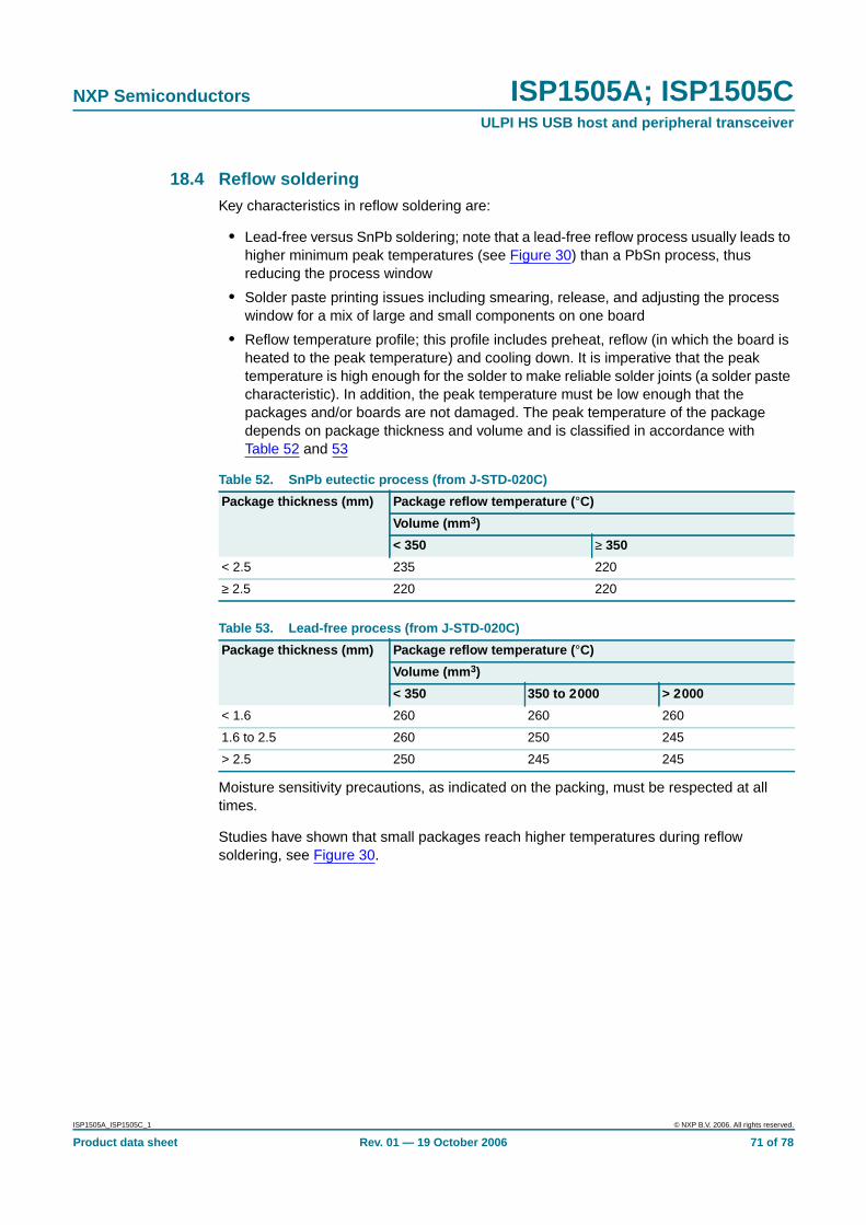
NXP Semiconductors ISP1505A; ISP1505CULPI HS USB host and peripheral transceiver
18.4 Reflow solderingKey characteristics in reflow soldering are:
• Lead-free versus SnPb soldering; note that a lead-free reflow process usually leads tohigher minimum peak temperatures (see Figure 30) than a PbSn process, thusreducing the process window
• Solder paste printing issues including smearing, release, and adjusting the processwindow for a mix of large and small components on one board
• Reflow temperature profile; this profile includes preheat, reflow (in which the board isheated to the peak temperature) and cooling down. It is imperative that the peaktemperature is high enough for the solder to make reliable solder joints (a solder pastecharacteristic). In addition, the peak temperature must be low enough that thepackages and/or boards are not damaged. The peak temperature of the packagedepends on package thickness and volume and is classified in accordance withTable 52 and 53
Moisture sensitivity precautions, as indicated on the packing, must be respected at alltimes.
Studies have shown that small packages reach higher temperatures during reflowsoldering, see Figure 30.
Table 52. SnPb eutectic process (from J-STD-020C)
Package thickness (mm) Package reflow temperature ( °C)
Volume (mm 3)
< 350 ≥ 350
< 2.5 235 220
≥ 2.5 220 220
Table 53. Lead-free process (from J-STD-020C)
Package thickness (mm) Package reflow temperature ( °C)
Volume (mm 3)
< 350 350 to 2000 > 2000
< 1.6 260 260 260
1.6 to 2.5 260 250 245
> 2.5 250 245 245
ISP1505A_ISP1505C_1 © NXP B.V. 2006. All rights reserved.
Product data sheet Rev. 01 — 19 October 2006 71 of 78

NXP Semiconductors ISP1505A; ISP1505CULPI HS USB host and peripheral transceiver
For further information on temperature profiles, refer to Application Note AN10365“Surface mount reflow soldering description”.
19. Abbreviations
MSL: Moisture Sensitivity Level
Fig 30. Temperature profiles for large and small components
001aac844
temperature
time
minimum peak temperature= minimum soldering temperature
maximum peak temperature= MSL limit, damage level
peak temperature
Table 54. Abbreviations
Acronym Description
ASIC Application-Specific Integrated Circuit
ATX Analog USB Transceiver
CD-RW Compact Disc-Rewritable
EOP End-Of-Packet
ESD ElectroStatic Discharge
FS Full-Speed
HBM Human Body Model
HNP Host Negotiation Protocol
HS High-Speed
ID Identification
LS Low-Speed
MO Magneto-Optical
NRZI Non-Return-to-Zero Inverted
OTG On-The-Go
PCB Printed-Circuit Board
PDA Personal Digital Assistant
PHY Physical Layer[1]
PID Packet Identifier
PLD Programmable Logic Device
ISP1505A_ISP1505C_1 © NXP B.V. 2006. All rights reserved.
Product data sheet Rev. 01 — 19 October 2006 72 of 78

NXP Semiconductors ISP1505A; ISP1505CULPI HS USB host and peripheral transceiver
[1] Physical layer containing the USB transceiver. The ISP1505 is a PHY.
20. References
[1] Universal Serial Bus Specification Rev. 2.0
[2] On-The-Go Supplement to the USB 2.0 Specification Rev. 1.2
[3] UTMI+ Low Pin Interface (ULPI) Specification Rev. 1.1
[4] UTMI+ Specification Rev. 1.0
[5] USB 2.0 Transceiver Macrocell Interface (UTMI) Specification Ver. 1.05
[6] Electrostatic Discharge (ESD) Sensitivity Testing Human Body Model (HBM)(JESD22-A114D)
[7] Interfacing to the ISP1504/5/6 (AN10048)
21. Revision history
PLL Phase-Locked Loop
POR Power-On Reset
RMS Root Mean Square
RoHS Restriction of Hazardous Substances
RXCMD Receive Command
SE0 Single-Ended Zero
SOF Start-Of-Frame
SRP Session Request Protocol
STB Set-Top Box
SYNC Synchronous
TTL Transistor-Transistor Logic
TXCMD Transmit Command
USB Universal Serial Bus
USB-IF USB Implementers Forum
ULPI UTMI+ Low Pin Interface
UTMI USB 2.0 Transceiver Macrocell Interface
UTMI+ USB 2.0 Transceiver Macrocell Interface Plus
Table 54. Abbreviations …continued
Acronym Description
Table 55. Revision history
Document ID Release date Data sheet status Change notice Supersedes
ISP1505A_ISP1505C_1 20061019 Product data sheet - -
ISP1505A_ISP1505C_1 © NXP B.V. 2006. All rights reserved.
Product data sheet Rev. 01 — 19 October 2006 73 of 78
NXP Semiconductors ISP1505A; ISP1505CULPI HS USB host and peripheral transceiver
22. Legal information
22.1 Data sheet status
[1] Please consult the most recently issued document before initiating or completing a design.
[2] The term ‘short data sheet’ is explained in section “Definitions”.
[3] The product status of device(s) described in this document may have changed since this document was published and may differ in case of multiple devices. The latest product statusinformation is available on the Internet at URL http://www.nxp.com.
22.2 Definitions
Draft — The document is a draft version only. The content is still underinternal review and subject to formal approval, which may result inmodifications or additions. NXP Semiconductors does not give anyrepresentations or warranties as to the accuracy or completeness ofinformation included herein and shall have no liability for the consequences ofuse of such information.
Short data sheet — A short data sheet is an extract from a full data sheetwith the same product type number(s) and title. A short data sheet is intendedfor quick reference only and should not be relied upon to contain detailed andfull information. For detailed and full information see the relevant full datasheet, which is available on request via the local NXP Semiconductors salesoffice. In case of any inconsistency or conflict with the short data sheet, thefull data sheet shall prevail.
22.3 Disclaimers
General — Information in this document is believed to be accurate andreliable. However, NXP Semiconductors does not give any representations orwarranties, expressed or implied, as to the accuracy or completeness of suchinformation and shall have no liability for the consequences of use of suchinformation.
Right to make changes — NXP Semiconductors reserves the right to makechanges to information published in this document, including withoutlimitation specifications and product descriptions, at any time and withoutnotice. This document supersedes and replaces all information supplied priorto the publication hereof.
Suitability for use — NXP Semiconductors products are not designed,authorized or warranted to be suitable for use in medical, military, aircraft,space or life support equipment, nor in applications where failure or
malfunction of a NXP Semiconductors product can reasonably be expected toresult in personal injury, death or severe property or environmental damage.NXP Semiconductors accepts no liability for inclusion and/or use of NXPSemiconductors products in such equipment or applications and thereforesuch inclusion and/or use is at the customer’s own risk.
Applications — Applications that are described herein for any of theseproducts are for illustrative purposes only. NXP Semiconductors makes norepresentation or warranty that such applications will be suitable for thespecified use without further testing or modification.
Limiting values — Stress above one or more limiting values (as defined inthe Absolute Maximum Ratings System of IEC 60134) may cause permanentdamage to the device. Limiting values are stress ratings only and operation ofthe device at these or any other conditions above those given in theCharacteristics sections of this document is not implied. Exposure to limitingvalues for extended periods may affect device reliability.
Terms and conditions of sale — NXP Semiconductors products are soldsubject to the general terms and conditions of commercial sale, as publishedat http://www.nxp.com/profile/terms, including those pertaining to warranty,intellectual property rights infringement and limitation of liability, unlessexplicitly otherwise agreed to in writing by NXP Semiconductors. In case ofany inconsistency or conflict between information in this document and suchterms and conditions, the latter will prevail.
No offer to sell or license — Nothing in this document may be interpretedor construed as an offer to sell products that is open for acceptance or thegrant, conveyance or implication of any license under any copyrights, patentsor other industrial or intellectual property rights.
22.4 TrademarksNotice: All referenced brands, product names, service names and trademarksare the property of their respective owners.
23. Contact information
For additional information, please visit: http://www .nxp.com
For sales office addresses, send an email to: salesad [email protected]
Document status [1] [2] Product status [3] Definition
Objective [short] data sheet Development This document contains data from the objective specification for product development.
Preliminary [short] data sheet Qualification This document contains data from the preliminary specification.
Product [short] data sheet Production This document contains the product specification.
ISP1505A_ISP1505C_1 © NXP B.V. 2006. All rights reserved.
Product data sheet Rev. 01 — 19 October 2006 74 of 78

NXP Semiconductors ISP1505A; ISP1505CULPI HS USB host and peripheral transceiver
24. Tables
Table 1. Ordering information . . . . . . . . . . . . . . . . . . . . .3Table 2. Pin description . . . . . . . . . . . . . . . . . . . . . . . . . .5Table 3. ULPI signal description . . . . . . . . . . . . . . . . . .14Table 4. Signal mapping during low-power mode . . . . .15Table 5. Signal mapping for 6-pin serial mode . . . . . . .16Table 6. Signal mapping for 3-pin serial mode . . . . . . .17Table 7. Operating states and resistor settings . . . . . . .17Table 8. TXCMD byte format . . . . . . . . . . . . . . . . . . . . .23Table 9. RXCMD byte format . . . . . . . . . . . . . . . . . . . . .24Table 10. LINESTATE[1:0] encoding for upstream
facing ports: peripherals . . . . . . . . . . . . . . . . .25Table 11. LINESTATE[1:0] encoding for downstream
facing ports: host . . . . . . . . . . . . . . . . . . . . . . .26Table 12. VBUS indicators in RXCMD for typical
applications . . . . . . . . . . . . . . . . . . . . . . . . . . .27Table 13. PHY pipeline delays . . . . . . . . . . . . . . . . . . . . .32Table 14. Link decision times . . . . . . . . . . . . . . . . . . . . .33Table 15. Register map overview . . . . . . . . . . . . . . . . . .45Table 16. Vendor ID Low register (address R = 00h)
bit description . . . . . . . . . . . . . . . . . . . . . . . . .45Table 17. Vendor ID High register (address R = 01h)
bit description . . . . . . . . . . . . . . . . . . . . . . . . .46Table 18. Product ID Low register (address R = 02h)
bit description . . . . . . . . . . . . . . . . . . . . . . . . .46Table 19. Product ID High register (address R = 03h)
bit description . . . . . . . . . . . . . . . . . . . . . . . . .46Table 20. Function Control register
(address R = 04h to 06h, W = 04h, S = 05h,C = 06h) bit allocation . . . . . . . . . . . . . . . . . . .46
Table 21. Function Control register(address R = 04h to 06h, W = 04h, S = 05h,C = 06h) bit description . . . . . . . . . . . . . . . . . .47
Table 22. Interface Control register(address R = 07h to 09h, W = 07h, S = 08h,C = 09h) bit allocation . . . . . . . . . . . . . . . . . . .47
Table 23. Interface Control register(address R = 07h to 09h, W = 07h, S = 08h,C = 09h) bit description . . . . . . . . . . . . . . . . . .48
Table 24. OTG Control register(address R = 0Ah to 0Ch, W = 0Ah, S = 0Bh,C = 0Ch) bit allocation . . . . . . . . . . . . . . . . . . .48
Table 25. OTG Control register(address R = 0Ah to 0Ch, W = 0Ah, S = 0Bh,C = 0Ch) bit description . . . . . . . . . . . . . . . . . .49
Table 26. USB Interrupt Enable Rising Edge register(address R = 0Dh to 0Fh, W = 0Dh, S = 0Eh,C = 0Fh) bit allocation . . . . . . . . . . . . . . . . . . .49
Table 27. USB Interrupt Enable Rising Edge register
(address R = 0Dh to 0Fh, W = 0Dh, S = 0Eh,C = 0Fh) bit description . . . . . . . . . . . . . . . . . . 50
Table 28. USB Interrupt Enable Falling Edge register(address R = 10h to 12h, W = 10h, S = 11h,C = 12h) bit allocation . . . . . . . . . . . . . . . . . . . 50
Table 29. USB Interrupt Enable Falling Edge register(address R = 10h to 12h, W = 10h, S = 11h,C = 12h) bit description . . . . . . . . . . . . . . . . . . 50
Table 30. USB Interrupt Status register(address R = 13h) bit allocation . . . . . . . . . . . 50
Table 31. USB Interrupt Status register(address R = 13h) bit description . . . . . . . . . . 51
Table 32. USB Interrupt Latch register(address R = 14h) bit allocation . . . . . . . . . . . 51
Table 33. USB Interrupt Latch register(address R = 14h) bit description . . . . . . . . . . 51
Table 34. Debug register (address R = 15h)bit allocation . . . . . . . . . . . . . . . . . . . . . . . . . . 51
Table 35. Debug register (address R = 15h)bit description . . . . . . . . . . . . . . . . . . . . . . . . . 52
Table 36. Scratch register (address R = 16h to 18h,W = 16h, S = 17h, C = 18h) bit description . . . 52
Table 37. Power Control register (address R = 3Dh to 3Fh,W = 3Dh, S = 3Eh, C = 3Fh) bit allocation . . . 52
Table 38. Power Control register (address R = 3Dh to 3Fh,W = 3Dh, S = 3Eh, C = 3Fh) bit description . . 53
Table 39. Limiting values . . . . . . . . . . . . . . . . . . . . . . . . . 55Table 40. Recommended operating conditions . . . . . . . . 55Table 41. Static characteristics: supply pins . . . . . . . . . . 56Table 42. Static characteristics: digital pins (CLOCK, DIR,
STP, NXT, DATA[7:0], RESET_N/PSW_N) . . . 56Table 43. Static characteristics: pin VBUS/FAULT . . . . . . 57Table 44. Static characteristics: analog I/O pins
(DP, DM) . . . . . . . . . . . . . . . . . . . . . . . . . . . . . 57Table 45. Static characteristics: VBUS comparators . . . . 59Table 46. Static characteristics: VBUS resistors . . . . . . . . 59Table 47. Static characteristics: resistor reference . . . . . 59Table 48. Dynamic characteristics: reset and clock . . . . 60Table 49. Dynamic characteristics: digital I/O pins . . . . . 61Table 50. Dynamic characteristics: analog I/O pins
(DP, DM) . . . . . . . . . . . . . . . . . . . . . . . . . . . . . 62Table 51. Recommended bill of materials . . . . . . . . . . . . 65Table 52. SnPb eutectic process (from J-STD-020C) . . . 71Table 53. Lead-free process (from J-STD-020C) . . . . . . 71Table 54. Abbreviations . . . . . . . . . . . . . . . . . . . . . . . . . . 72Table 55. Revision history . . . . . . . . . . . . . . . . . . . . . . . . 73
ISP1505A_ISP1505C_1 © NXP B.V. 2006. All rights reserved.
Product data sheet Rev. 01 — 19 October 2006 75 of 78
continued >>

NXP Semiconductors ISP1505A; ISP1505CULPI HS USB host and peripheral transceiver
25. Figures
Fig 1. Block diagram . . . . . . . . . . . . . . . . . . . . . . . . . . . .4Fig 2. Pin configuration HVQFN24; top view . . . . . . . . . .5Fig 3. Internal power-on reset timing . . . . . . . . . . . . . . .19Fig 4. Power-up and reset sequence required before
the ULPI bus is ready for use. . . . . . . . . . . . . . . .21Fig 5. Interface behavior with respect to RESET_N. . . .22Fig 6. Single and back-to-back RXCMDs from the
ISP1505 to the link. . . . . . . . . . . . . . . . . . . . . . . .25Fig 7. RXCMD A_VBUS_VLD indicator source . . . . . . .26Fig 8. Example of register write, register read,
extended register write and extendedregister read. . . . . . . . . . . . . . . . . . . . . . . . . . . . .29
Fig 9. USB reset and high-speed detectionhandshake (chirp) sequence . . . . . . . . . . . . . . . .31
Fig 10. Example of using the ISP1505 to transmit andreceive USB data . . . . . . . . . . . . . . . . . . . . . . . . .32
Fig 11. High-speed transmit-to-transmit packet timing. . .33Fig 12. High-speed receive-to-transmit packet timing . . .34Fig 13. Preamble sequence . . . . . . . . . . . . . . . . . . . . . . .35Fig 14. Full-speed suspend and resume . . . . . . . . . . . . .36Fig 15. High-speed suspend and resume . . . . . . . . . . . .38Fig 16. Remote wake-up from low-power mode . . . . . . .40Fig 17. Transmitting USB packets without
the automatic SYNC and EOP generation. . . . . .41Fig 18. Example of transmit followed by receive
in 6-bit serial mode . . . . . . . . . . . . . . . . . . . . . . .43Fig 19. Example of transmit followed by receive
in 3-bit serial mode . . . . . . . . . . . . . . . . . . . . . . .43Fig 20. Human body ESD test model. . . . . . . . . . . . . . . .54Fig 21. Rise time and fall time . . . . . . . . . . . . . . . . . . . . .64Fig 22. Timing of TX_DAT and TX_SE0 to DP and DM. .64Fig 23. Timing of TX_ENABLE to DP and DM. . . . . . . . .64Fig 24. Timing of DP and DM to RX_RCV, RX_DP
and RX_DM . . . . . . . . . . . . . . . . . . . . . . . . . . . . .64Fig 25. ULPI timing interface . . . . . . . . . . . . . . . . . . . . . .64Fig 26. Using the ISP1505 with a USB Host Controller;
external 5 V source with built-in FAULTand external crystal . . . . . . . . . . . . . . . . . . . . . . .66
Fig 27. Using the ISP1505 with a Peripheral Controller;external 60 MHz input on CLOCK . . . . . . . . . . . .67
Fig 28. Using the ISP1505 with a Peripheral Controller;external square wave input on pin XTAL1 . . . . . .68
Fig 29. Package outline SOT616-1 (HVQFN24) . . . . . . .69Fig 30. Temperature profiles for large and small
components . . . . . . . . . . . . . . . . . . . . . . . . . . . . .72
ISP1505A_ISP1505C_1 © NXP B.V. 2006. All rights reserved.
Product data sheet Rev. 01 — 19 October 2006 76 of 78
continued >>
NXP Semiconductors ISP1505A; ISP1505CULPI HS USB host and peripheral transceiver
26. Contents
1 General description . . . . . . . . . . . . . . . . . . . . . . 12 Features . . . . . . . . . . . . . . . . . . . . . . . . . . . . . . . 13 Applications . . . . . . . . . . . . . . . . . . . . . . . . . . . . 24 Ordering information . . . . . . . . . . . . . . . . . . . . . 35 Block diagram . . . . . . . . . . . . . . . . . . . . . . . . . . 46 Pinning information . . . . . . . . . . . . . . . . . . . . . . 56.1 Pinning . . . . . . . . . . . . . . . . . . . . . . . . . . . . . . . 56.2 Pin description . . . . . . . . . . . . . . . . . . . . . . . . . 57 Functional description . . . . . . . . . . . . . . . . . . . 77.1 ULPI interface controller . . . . . . . . . . . . . . . . . . 77.2 USB serializer and deserializer. . . . . . . . . . . . . 77.3 Hi-Speed USB (USB 2.0) ATX . . . . . . . . . . . . . 77.4 Voltage regulator. . . . . . . . . . . . . . . . . . . . . . . . 87.5 Crystal oscillator and PLL. . . . . . . . . . . . . . . . . 87.6 VBUS comparators. . . . . . . . . . . . . . . . . . . . . . . 87.6.1 VBUS valid comparator . . . . . . . . . . . . . . . . . . . 87.6.2 Session valid comparator . . . . . . . . . . . . . . . . . 97.6.3 Session end comparator. . . . . . . . . . . . . . . . . . 97.7 SRP charge and discharge resistors . . . . . . . . 97.8 Band gap reference voltage . . . . . . . . . . . . . . . 97.9 Power-on reset . . . . . . . . . . . . . . . . . . . . . . . . . 97.10 Detailed description of pins . . . . . . . . . . . . . . . 97.10.1 DATA[7:0] . . . . . . . . . . . . . . . . . . . . . . . . . . . . . 97.10.2 VCC(I/O) . . . . . . . . . . . . . . . . . . . . . . . . . . . . . . 107.10.3 RREF . . . . . . . . . . . . . . . . . . . . . . . . . . . . . . . 107.10.4 DP and DM . . . . . . . . . . . . . . . . . . . . . . . . . . . 107.10.5 VCC . . . . . . . . . . . . . . . . . . . . . . . . . . . . . . . . . 107.10.6 VBUS/FAULT . . . . . . . . . . . . . . . . . . . . . . . . . . 107.10.6.1 VBUS . . . . . . . . . . . . . . . . . . . . . . . . . . . . . . . . 107.10.6.2 FAULT (external overcurrent or fault detector) 107.10.7 REG3V3 and REG1V8 . . . . . . . . . . . . . . . . . . 117.10.8 XTAL1 and XTAL2. . . . . . . . . . . . . . . . . . . . . . 117.10.9 RESET_N/PSW_N . . . . . . . . . . . . . . . . . . . . . 117.10.9.1 RESET_N . . . . . . . . . . . . . . . . . . . . . . . . . . . . 117.10.9.2 PSW_N. . . . . . . . . . . . . . . . . . . . . . . . . . . . . . 117.10.10 DIR . . . . . . . . . . . . . . . . . . . . . . . . . . . . . . . . . 127.10.11 STP. . . . . . . . . . . . . . . . . . . . . . . . . . . . . . . . . 127.10.12 NXT. . . . . . . . . . . . . . . . . . . . . . . . . . . . . . . . . 127.10.13 CLOCK . . . . . . . . . . . . . . . . . . . . . . . . . . . . . . 127.10.14 GND (die pad). . . . . . . . . . . . . . . . . . . . . . . . . 138 Modes of operation . . . . . . . . . . . . . . . . . . . . . 148.1 ULPI modes . . . . . . . . . . . . . . . . . . . . . . . . . . 148.1.1 Synchronous mode. . . . . . . . . . . . . . . . . . . . . 148.1.2 Low-power mode . . . . . . . . . . . . . . . . . . . . . . 158.1.3 6-pin full-speed or low-speed serial mode . . . 168.1.4 3-pin full-speed or low-speed serial mode . . . 16
8.2 USB and OTG state transitions . . . . . . . . . . . 179 Protocol description . . . . . . . . . . . . . . . . . . . . 199.1 ULPI references . . . . . . . . . . . . . . . . . . . . . . . 199.2 Power-On Reset (POR) . . . . . . . . . . . . . . . . . 199.3 Power-up, reset and bus idle sequence . . . . . 199.3.1 Interface protection. . . . . . . . . . . . . . . . . . . . . 229.3.2 Interface behavior with respect to RESET_N. 229.4 VBUS power and fault detection . . . . . . . . . . . 229.4.1 Driving 5 V on VBUS . . . . . . . . . . . . . . . . . . . . 229.4.2 Fault detection . . . . . . . . . . . . . . . . . . . . . . . . 239.5 TXCMD and RXCMD . . . . . . . . . . . . . . . . . . . 239.5.1 TXCMD . . . . . . . . . . . . . . . . . . . . . . . . . . . . . 239.5.2 RXCMD . . . . . . . . . . . . . . . . . . . . . . . . . . . . . 249.5.2.1 Linestate encoding . . . . . . . . . . . . . . . . . . . . . 259.5.2.2 VBUS state encoding. . . . . . . . . . . . . . . . . . . . 269.5.2.3 RxEvent encoding . . . . . . . . . . . . . . . . . . . . . 279.6 Register read and write operations . . . . . . . . 289.7 USB reset and high-speed detection
handshake (chirp) . . . . . . . . . . . . . . . . . . . . . 299.8 USB packet transmit and receive . . . . . . . . . . 329.8.1 USB packet timing . . . . . . . . . . . . . . . . . . . . . 329.8.1.1 ISP1505 pipeline delays. . . . . . . . . . . . . . . . . 329.8.1.2 Allowed link decision time . . . . . . . . . . . . . . . 329.9 Preamble . . . . . . . . . . . . . . . . . . . . . . . . . . . . 349.10 USB suspend and resume . . . . . . . . . . . . . . . 359.10.1 Full-speed and low-speed host-initiated
suspend and resume . . . . . . . . . . . . . . . . . . . 359.10.2 High-speed suspend and resume . . . . . . . . . 369.10.3 Remote wake-up . . . . . . . . . . . . . . . . . . . . . . 399.11 No automatic SYNC and EOP generation
(optional) . . . . . . . . . . . . . . . . . . . . . . . . . . . . 409.12 On-The-Go operations . . . . . . . . . . . . . . . . . . 419.12.1 OTG comparators. . . . . . . . . . . . . . . . . . . . . . 429.12.2 Pull-up and pull-down resistors . . . . . . . . . . . 429.12.3 VBUS charge and discharge resistors . . . . . . . 429.13 Serial modes . . . . . . . . . . . . . . . . . . . . . . . . . 429.14 Aborting transfers. . . . . . . . . . . . . . . . . . . . . . 449.15 Avoiding contention on the ULPI data bus . . . 4410 Register map . . . . . . . . . . . . . . . . . . . . . . . . . . 4510.1 Immediate register set . . . . . . . . . . . . . . . . . . 4510.1.1 Vendor ID and Product ID registers . . . . . . . . 4510.1.1.1 Vendor ID Low register. . . . . . . . . . . . . . . . . . 4510.1.1.2 Vendor ID High register . . . . . . . . . . . . . . . . . 4610.1.1.3 Product ID Low register . . . . . . . . . . . . . . . . . 4610.1.1.4 Product ID High register. . . . . . . . . . . . . . . . . 4610.1.2 Function Control register . . . . . . . . . . . . . . . . 4610.1.3 Interface Control register . . . . . . . . . . . . . . . . 47
ISP1505A_ISP1505C_1 © NXP B.V. 2006. All rights reserved.
Product data sheet Rev. 01 — 19 October 2006 77 of 78
continued >>
NXP Semiconductors ISP1505A; ISP1505CULPI HS USB host and peripheral transceiver
10.1.4 OTG Control register . . . . . . . . . . . . . . . . . . . 4810.1.5 USB Interrupt Enable Rising Edge register . . 4910.1.6 USB Interrupt Enable Falling Edge register . . 5010.1.7 USB Interrupt Status register . . . . . . . . . . . . . 5010.1.8 USB Interrupt Latch register . . . . . . . . . . . . . . 5110.1.9 Debug register . . . . . . . . . . . . . . . . . . . . . . . . 5110.1.10 Scratch register. . . . . . . . . . . . . . . . . . . . . . . . 5210.1.11 Reserved . . . . . . . . . . . . . . . . . . . . . . . . . . . . 5210.1.12 Access extended register set . . . . . . . . . . . . . 5210.1.13 Vendor-specific registers . . . . . . . . . . . . . . . . 5210.1.14 Power Control register . . . . . . . . . . . . . . . . . . 5210.2 Extended register set . . . . . . . . . . . . . . . . . . . 5311 ElectroStatic Discharge (ESD) . . . . . . . . . . . . 5411.1 ESD protection . . . . . . . . . . . . . . . . . . . . . . . . 5411.2 ESD test conditions . . . . . . . . . . . . . . . . . . . . 5412 Limiting values. . . . . . . . . . . . . . . . . . . . . . . . . 5513 Recommended operating conditions. . . . . . . 5514 Static characteristics. . . . . . . . . . . . . . . . . . . . 5615 Dynamic characteristics . . . . . . . . . . . . . . . . . 6015.1 ULPI timing . . . . . . . . . . . . . . . . . . . . . . . . . . . 6416 Application information. . . . . . . . . . . . . . . . . . 6517 Package outline . . . . . . . . . . . . . . . . . . . . . . . . 6918 Soldering . . . . . . . . . . . . . . . . . . . . . . . . . . . . . 7018.1 Introduction to soldering . . . . . . . . . . . . . . . . . 7018.2 Wave and reflow soldering . . . . . . . . . . . . . . . 7018.3 Wave soldering . . . . . . . . . . . . . . . . . . . . . . . . 7018.4 Reflow soldering . . . . . . . . . . . . . . . . . . . . . . . 7119 Abbreviations . . . . . . . . . . . . . . . . . . . . . . . . . . 7220 References . . . . . . . . . . . . . . . . . . . . . . . . . . . . 7321 Revision history . . . . . . . . . . . . . . . . . . . . . . . . 7322 Legal information. . . . . . . . . . . . . . . . . . . . . . . 7422.1 Data sheet status . . . . . . . . . . . . . . . . . . . . . . 7422.2 Definitions . . . . . . . . . . . . . . . . . . . . . . . . . . . . 7422.3 Disclaimers . . . . . . . . . . . . . . . . . . . . . . . . . . . 7422.4 Trademarks . . . . . . . . . . . . . . . . . . . . . . . . . . . 7423 Contact information. . . . . . . . . . . . . . . . . . . . . 7424 Tables . . . . . . . . . . . . . . . . . . . . . . . . . . . . . . . . 7525 Figures . . . . . . . . . . . . . . . . . . . . . . . . . . . . . . . 7626 Contents . . . . . . . . . . . . . . . . . . . . . . . . . . . . . . 77
© NXP B.V. 2006. All rights reserved.For more information, please visit: http://www.nxp.comFor sales office addresses, please send an email to: [email protected]
Date of release: 19 October 2006
Document identifier: ISP1505A_ISP1505C_1
Please be aware that important notices concerning this document and the product(s)described herein, have been included in section ‘Legal information’.