Embed Size (px)
Citation preview

VOLUME 19, NUMBER 1, 2012 n LINCOLN LABORATORY JOURNAL 51
Isolation Improvement with Electromagnetic Band Gap SurfacesJohn Sandora
An electromagnetic band gap (EBG)
material is a periodic surface specifically
designed to have certain electromagnetic
properties at specific frequencies. The term
“metamaterial” is sometimes used to describe such engi-
neered surfaces. Metamaterials (“meta” means “beyond”
in Greek) are man-made materials not found in nature
and designed by placing tiny resonant structures at regu-
larly spaced distances to create the appearance of a differ-
ent bulk propagation medium [1]. As long as the inserted
structures, called cells, are very small compared to the
propagating wavelength, they can create a macroscopic
effect on the electromagnetic wave as it passes through the
new medium. Figure 1 depicts the engineered material’s
macro/micro “atomic” geometry approximation and the
corresponding periodic unit cell. Desired electromagnetic
properties can include specific values of permittivity, per-
meability, reflected phase, and index of refraction. If such
media could be realized, then human beings could control
the propagation of electromagnetic waves in previously
unfeasible ways [1].*
EBGs are a class of metamaterials whose purpose is
to highly impede electromagnetic propagation along the
device’s surface within the frequency band of operation
known as a “band gap” (hence the name “electromagnetic
band gap” material) [2]. In this sense, it is an artificially
high-impedance surface and blocks current from flow-
ing at microwave frequencies. In contrast, normal metals
A new type of engineered surface called an electromagnetic band gap blocks current from flowing at microwave frequencies. One application of this metamaterial is to employ the surface amid electronic devices to improve the electromagnetic isolation between them. The different geometry features of the device’s individual unit cells create extra inductances and capacitances for electromagnetic waves. When the unit cell is properly tuned, the aggregate surface will block incoming signals just as a band-stop filter will. This additional isolation allows radio-frequency receivers to operate in closer proximity to transmitters than a normal metal surface would permit.
»
* We are always bounded by the laws of physics—in this case Maxwell’s equations. Metamaterials are merely different man-made materials for these same laws to act in.

52 LINCOLN LABORATORY JOURNAL n VOLUME 19, NUMBER 1, 2012
electromagnetic iSolation improvement with eBg SurfaceS
faces, and the EBG is shown to greatly improve isolation
for realistic test cases.
Electromagnetic Interference
A common problem with electronic systems is a lack
of electromagnetic isolation between closely spaced
devices [3]. Modern military vehicles often contain sev-
eral communication systems, early-warning receivers,
radar, and radar jammers that are all in close proxim-
ity to each other. Metallic surfaces between transmitters
and receivers allow current to propagate between sys-
tems with little impedance. Unfortunately, these systems
can interfere with each other, causing major electro-
magnetic interference and electromagnetic compatibil-
ity issues that prevent the optimum operation of each
individual system [3]. This problem is intensified by the
vehicle body itself. Figure 2a shows a computer simula-
tion of a snapshot in time of the electric-field intensity
generated by a transmitting UHF antenna at the nose
of a helicopter. Red indicates higher intensity; blue is
have very low impedance to current and allow it to flow
over the entire metal surface. Impeding surface currents
has immediate application to the field of antenna design,
where metal ground planes have traditionally imposed
constraints on both the minimum antenna size and cor-
rupted the directivity pattern. The EBG was conceived
as a potential solution by Daniel Sievenpiper and other
researchers at the University of California at Los Angeles,
who first constructed the unit cell geometry and investi-
gated its properties [2].
This article describes another application of EBGs:
employing the surface amid electronic devices to improve
electromagnetic isolation between them. The small fea-
tures of the periodic surface are easily manufactured by
modern printed-circuit-board (PCB) companies. Com-
putational analysis techniques such as the finite-element
method (FEM) are shown to enable the design and opti-
mization of the periodic unit cell geometry for particular
frequency bands. Measured results show the comparison
between bare metal, absorber materials, and EBG sur-
figure 1. The bulk or macroscopic scale of the metamaterial is broken down into microcomponents in a repeated two-dimensional pattern. The physical properties of the microcomponents are the basis for the electromagnetic band gap (EBG) responses to radio-frequency propagation.
figure 2. A numerical simulation for the electric-field intensity for a UHF transmitter on a helicopter nose (a) shows sig-nificant magnitudes throughout the air surrounding the entire helicopter. The electric-field intensity shown in (a) generates resulting currents in the helicopter itself (b). This current can cause interference with other onboard systems.
(a) (b)
VOLUME 19, NUMBER 1, 2012 n LINCOLN LABORATORY JOURNAL 53
John Sandora
the lowest intensity. These electromagnetic fields enable
communication by radiating energy, but they also excite
electric currents that run along the surface of the air-
frame. Figure 2b shows a similar snapshot in time of the
electric-current intensity on the surface of the helicopter.
It shows that these currents run along the entire airframe
and will possibly interfere with other electromagnetic
devices on board.
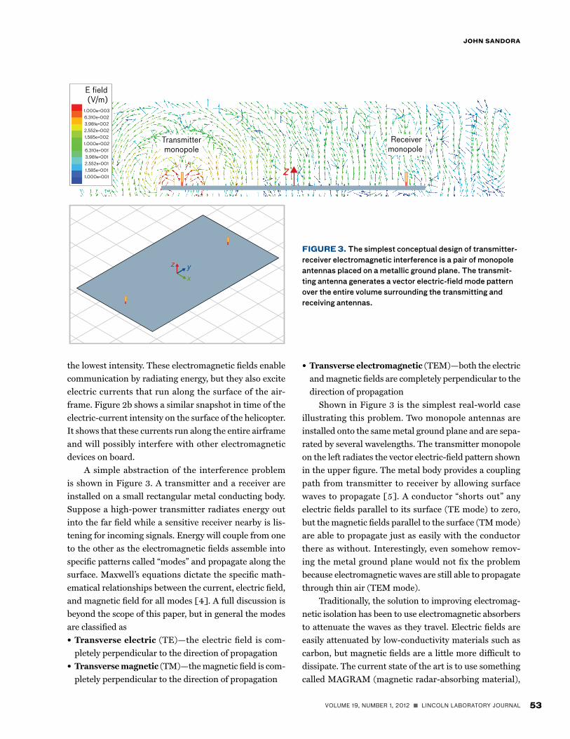
A simple abstraction of the interference problem
is shown in Figure 3. A transmitter and a receiver are
installed on a small rectangular metal conducting body.
Suppose a high-power transmitter radiates energy out
into the far field while a sensitive receiver nearby is lis-
tening for incoming signals. Energy will couple from one
to the other as the electromagnetic fields assemble into
specific patterns called “modes” and propagate along the
surface. Maxwell’s equations dictate the specific math-
ematical relationships between the current, electric field,
and magnetic field for all modes [4]. A full discussion is
beyond the scope of this paper, but in general the modes
are classified as
•Transverse electric (TE) —the electric field is com-
pletely perpendicular to the direction of propagation
•Transverse magnetic (TM)—the magnetic field is com-
pletely perpendicular to the direction of propagation
•Transverse electromagnetic (TEM)—both the electric
and magnetic fields are completely perpendicular to the
direction of propagation
Shown in Figure 3 is the simplest real-world case
illustrating this problem. Two monopole antennas are
installed onto the same metal ground plane and are sepa-
rated by several wavelengths. The transmitter monopole
on the left radiates the vector electric-field pattern shown
in the upper figure. The metal body provides a coupling
path from transmitter to receiver by allowing surface
waves to propagate [5]. A conductor “shorts out” any
electric fields parallel to its surface (TE mode) to zero,
but the magnetic fields parallel to the surface (TM mode)
are able to propagate just as easily with the conductor
there as without. Interestingly, even somehow remov-
ing the metal ground plane would not fix the problem
because electromagnetic waves are still able to propagate
through thin air (TEM mode).
Traditionally, the solution to improving electromag-
netic isolation has been to use electromagnetic absorbers
to attenuate the waves as they travel. Electric fields are
easily attenuated by low-conductivity materials such as
carbon, but magnetic fields are a little more difficult to
dissipate. The current state of the art is to use something
called MAGRAM (magnetic radar-absorbing material),
xz y
figure 3. The simplest conceptual design of transmitter-receiver electromagnetic interference is a pair of monopole antennas placed on a metallic ground plane. The transmit-ting antenna generates a vector electric-field mode pattern over the entire volume surrounding the transmitting and receiving antennas.
z
1.000e+0036.310e+002
1.000e+002
2.552e+0023.981e+002
1.585e+002
1.000e+001
6.310e+001
2.552e+0013.981e+001
1.585e+001
E field (V/m)
Transmitter monopole
Receivermonopole

54 LINCOLN LABORATORY JOURNAL n VOLUME 19, NUMBER 1, 2012
electromagnetic iSolation improvement with eBg SurfaceS
figure 4. One example of an EBG textured-surface metamaterial is multiple cells with small gaps in two dimensions. On the right is shown a metal surface with the equivalent geometry to the EBG plate. In this configuration, the small dots centered at the top and bottom of the device are the transmitter/receiver pair. Each of these test boards is approximately 3 inches by 5 inches.
figure 5. The electric-field intensity generated by the transmitting monopole (on the left) is shown for three cases: on a metal ground plane (top), with a MAGRAM absorber sheet (middle), and with an EBG sur-face (bottom). The improvements are clearly evident when MAGRAM is added to the ground plane and, more significantly, when EBG is present.
z
z
z

VOLUME 19, NUMBER 1, 2012 n LINCOLN LABORATORY JOURNAL 55
John Sandora
which consists of tiny iron beads encased in a thick rubber
sheet [6]. The iron beads are densely packed throughout
the sheet so that as the wave progresses, it excites eddy
currents that run around the perimeter of each bead. Cre-
ating these extra currents takes additional energy so there
is attenuation as the wave propagates through the mate-
rial. MAGRAM’s limitations are that it is heavy and not
very effective over short distances. The solution presented
next is an attempt to greatly improve isolation by blocking
the waves from propagating at all.
Electromagnetic Band Gap Surfaces
An EBG structure is a new class of engineered surface.
By carefully designing the texture of this surface, over the
operating frequency range known as the band gap, we can
do better than attenuating the waves—we can prevent
them from propagating altogether [2]. Figure 4 shows an
example EBG surface. Since we understand the modes that
can transport energy, the concept of the surface develop-
ment—adding specific textures onto the surface —can pre-
vent these modes from being set up. If no modes are able
to exist, electromagnetic energy cannot propagate. When
faced with no other alternative, the electromagnetic waves
lift up off the surface and radiate out into the surrounding
space.
Figure 5 illustrates three relevant cases. First, the
top image in Figure 5 shows a computer simulation of
the electric-field intensity for the baseline case shown in
Figure 3, two monopoles over a metal ground plane. The
next image is of the electric-field intensity for the same
geometry with a sheet of MAGRAM on top of the ground
plane. The electric-field intensity decreases from left to
right, indicating attenuation as the wave travels. The bot-
tom image is for an EBG layer on top of the metal ground
plane. In this case, the fields are shown to have extreme
difficulty propagating along the surface, and instead radi-
ate upwards away from the receiving monopole antenna.
The color scale is the same for all three images.
Electromagnetic Analysis
The EBG structure, shown in Figure 4, is actually a simple
unit cell repeated many times to form a surface. Each unit
cell has three parts: the bottom metal ground plane layer,
a square metal hat on top, and a conducting via between
the two, as shown in Figure 6. The dimensions of the hat
are carefully determined such that there is a specific gap
in between neighbors in all directions. Although it is not
required, a dielectric substrate usually exists between the
two metal layers for both mechanical support and ease of
fabrication with PCB techniques. Each unit cell’s along-
the-plane dimensions must be a small fraction of a wave-
length in the operating range in order for the surface as
a whole to appear electromagnetically homogeneous [7].
The unit cell dimensions are 2.25 mm for the hat length
and width, along with a 0.38 mm diameter via. The gap
between neighboring hats is 0.15 mm. The substrate used
is a 4.1 mm thick version of a common radio-frequency
(RF) PCB core called RO5880 (from the Rogers Corpora-
tion). It has a dielectric constant (er) of 2.2 and a loss tan-
gent (tan d) of 0.002. This EBG was fabricated by etching
away the gap regions of the copper on the top side of a
RO5880 core. The conductive vias are “through holes”
drilled and then plated through with nickel.
As stated previously, the EBG ability to block elec-
tromagnetic radiation transmission hinges upon having
a unit cell such that it is impossible for any electromag-
netic modes to exist on the surface. For certain geometry
combinations of gap, height, and via diameter, radiation
blockage is possible over a limited band gap frequency
range. Interestingly, it is not necessary for the fields and
current to be zero on every unit cell, nor is it required
Gap
Substrateheight
Viadiameter
Hat size
figure 6. Individual EBG unit cell components are com-bined in two dimensions to create the surface. The hat size is slightly smaller than the substrate size. The gap dimen-sions versus hat size can be tuned to respond to appropriate frequency ranges.
56 LINCOLN LABORATORY JOURNAL n VOLUME 19, NUMBER 1, 2012
electromagnetic iSolation improvement with eBg SurfaceS
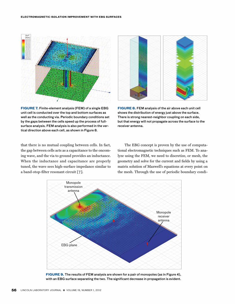
figure 7. Finite-element analysis (FEM) of a single EBG unit cell is conducted over the top and bottom surfaces as well as the conducting via. Periodic boundary conditions set by the gaps between the cells speed up the process of full-surface analysis. FEM analysis is also performed in the ver-tical direction above each cell, as shown in Figure 8.
figure 8. FEM analysis of the air above each unit cell shows the distribution of energy just above the surface. There is strong nearest-neighbor coupling on each side, but that energy will not propagate across the surface to the receiver antenna.
EBG plane
Monopoletransmission
antenna
Monopolereceiverantenna
z
figure 9. The results of FEM analysis are shown for a pair of monopoles (as in Figure 4), with an EBG surface separating the two. The significant decrease in propagation is evident.
2.232e+0022.092e+002
1.534e+002
1.813e+0021.953e+002
1.674e+002
8.373e+001
1.395e+002
1.116e+0021.256e+002
9.767e+001
6.453e-002
5.584e+001
1.401e+0012.795e+0014.190e+001
6.978e+001
Jsurf(A/m)
that there is no mutual coupling between cells. In fact,
the gap between cells acts as a capacitance to the oncom-
ing wave, and the via to ground provides an inductance.
When the inductance and capacitance are properly
tuned, the wave sees high-surface impedance similar to
a band-stop-filter resonant circuit [7].
The EBG concept is proven by the use of computa-
tional electromagnetic techniques such as FEM. To ana-
lyze using the FEM, we need to discretize, or mesh, the
geometry and solve for the current and fields by using a
matrix solution of Maxwell’s equations at every point on
the mesh. Through the use of periodic boundary condi-

VOLUME 19, NUMBER 1, 2012 n LINCOLN LABORATORY JOURNAL 57
John Sandora
tions on the unit cell walls, we can solve one unit cell vir-
tually embedded in an infinitely large EBG surface [8].
Periodic boundary conditions allow for the solution of a
single unit cell while still including mutual coupling effects
from all neighboring cells [9]. Figure 7 shows an example
mesh and current-intensity plot for the EBG unit cell for a
single mode. Figures 8 and 9 illustrate the FEM analysis of
the atmosphere above a unit cell and the resulting surface
intensity, respectively. In order to improve the isolation for
real-world systems and not merely illustrate an academic
curiosity, we must ensure that all propagating modes are
blocked. This requires solving for the currents and fields
using the FEM to obtain a complete set of modes and
determining which modes will propagate by using a dis-
persion diagram, such as the one shown in Figure 10.
A dispersion diagram is equivalent to the Bloch dia-
grams used to illustrate the energy-band structures in
periodic crystalline media [10]. The two lowest-order
modes shown in Figure 10 are plotted as curves of the
frequency at which the mode occurs versus wave vector.
The frequency band in between the two mode curves is
where no modes can exist for a given wave vector; this is
the band gap. Although it is mathematically complete,
one of the problems with the dispersion diagram is that it
is computationally intensive. Because each point requires
a full FEM solution, it therefore is not well suited for a
practical design-flow procedure.
figure 10. Conventional unit cell analysis produces a dis-persion diagram showing the propagation modes and the associated band gap. Γ, X, and M are the wave vectors, and Mode 1 and Mode 2 are the transverse magnetic and trans-verse electric low-order eigenmodes.
Mode 2Mode 1
Speed of light boundary
Band gap
X M
35
45
15
510
20
0
30
40
50
25
Freq
uenc
y (G
Hz)
XM
Dispersion Diagram
Wave vector
figure 11. Electromagnetic image theory explains the in-phase and opposite-phase correlations between electric and magnetic fields at conducting surfaces [3].
Perfect electric conductorElectric Magnetic
Sources
Imageh
h
Perfect magnetic conductorElectric Magnetic
Sources
Imageh
h
Reflected phase versus frequency
Deg
rees
–90
45
0
180
–180
–135
–45
90
135
8 1610 1812 14Frequency (GHz)
Reflected phase versus frequency
Deg
rees
–90
45
0
180
–180
–135
–45
90
135
8 1610 1812 14Frequency (GHz)
58 LINCOLN LABORATORY JOURNAL n VOLUME 19, NUMBER 1, 2012
electromagnetic iSolation improvement with eBg SurfaceS
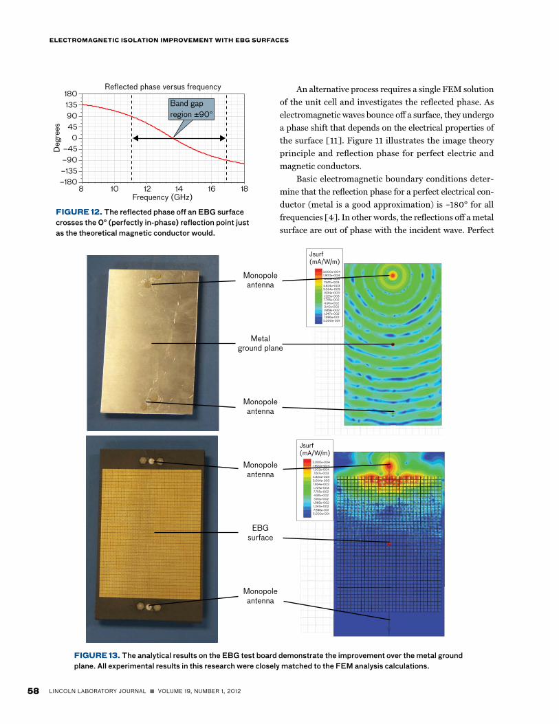
An alternative process requires a single FEM solution
of the unit cell and investigates the reflected phase. As
electromagnetic waves bounce off a surface, they undergo
a phase shift that depends on the electrical properties of
the surface [11]. Figure 11 illustrates the image theory
principle and reflection phase for perfect electric and
magnetic conductors.
Basic electromagnetic boundary conditions deter-
mine that the reflection phase for a perfect electrical con-
ductor (metal is a good approximation) is –180° for all
frequencies [4]. In other words, the reflections off a metal
surface are out of phase with the incident wave. Perfect
Reflected phase versus frequency
–180–135 –90 –45
0 45 90 135 180
Deg
rees
Frequency (GHz)8 1816141210
Band gapregion ±90°
figure 12. The reflected phase off an EBG surface crosses the 0° (perfectly in-phase) reflection point just as the theoretical magnetic conductor would.
figure 13. The analytical results on the EBG test board demonstrate the improvement over the metal ground plane. All experimental results in this research were closely matched to the FEM analysis calculations.
3.000e+0041.900e+004
3.054e+003
7.617e+0031.203e+004
4.824e+003
3.110e+002
1.934e+003
7.755e+0021.225e+003
4.911e+002
7.896e+0015.000e+001
1.247e+0021.969e+002
Jsurf (mA/W/m)
3.000e+0041.900e+004
3.054e+003
7.617e+0031.203e+004
4.824e+003
3.110e+002
1.934e+003
7.755e+0021.225e+003
4.911e+002
7.896e+0015.000e+001
1.247e+0021.969e+002
Jsurf (mA/W/m)
Monopoleantenna
Metalground plane
Monopoleantenna
Monopoleantenna
Monopoleantenna
EBGsurface

VOLUME 19, NUMBER 1, 2012 n LINCOLN LABORATORY JOURNAL 59
John Sandora
magnetic conductors do not exist in real life, but are only
postulated in electromagnetic theory. If such a surface
existed, it would have the property that reflected waves
would have 0° phase shift and be perfectly in phase with
the incident wave [4].
One of the reasons that EBGs have generated such
excitement in the field of electromagnetics is because,
within their band gap, they approximate certain charac-
teristics of the purely theoretical magnetic conductor [2].
The theoretical becoming practical first becomes evident
upon noting the reflected phase off an EBG surface as
shown in Figure 12. The EBG appears to have reflected
phase properties similar to the theoretical magnetic con-
ductor. An alternative definition of the band gap could
be the frequency range for which the reflected phase is
within ±90°, because within this frequency range the
reflections off the EBG surface are at least partly in phase
with the incident wave. As will be shown next, these ±90°
frequency points map approximately onto the frequen-
cies for which the EBG blocks surface waves. So although
the reflection phase has interesting applications for low-
profile antennas, which can be placed flat onto an EBG
surface (and have their reflections still add up in phase),
in this context it is an efficient design procedure for the
isolation problem [12]. Now we have a simple way to
determine the band gap frequencies accurately from a
single unit cell simulation.
Isolation Improvement
The theoretical electromagnetic implications of textured
surfaces discussed in the previous section have been an
intense area of research in the academic community, but
the practical benefits of having such a surface that can
“block current” is very real-world. Through numerical
simulations of the reflected phase, we have shown a simple
way to determine the band gap range of frequencies from
a single unit cell simulation. But simulating a realistic-
sized EBG with thousands of unit cells is well beyond the
capability of today’s computers. Therefore, accurately
determining the isolation improvement that the EBG can
provide must be determined experimentally.
Now that a straightforward design procedure has been
found, the next step is to develop a test case to determine
how well the EBG performs in the real world. Figure 13
shows the set of experimental conditions to measure the
baseline isolation between two antennas. The top left image
is a top-down view of the actual monopole antennas on a
normal metal ground plane. The ground plane dimensions
are 3 inches wide by 5 inches long, with a 4-inch spacing
in between the two antennas. The right image is a current-
intensity simulation for this baseline case.
The bottom left side of Figure 13 is the EBG test board.
It is has the same outer dimensions as the metal plate (3 ×
5 inches) and has an identical metal ground plane, but the
center 3.75 inches are now covered with EBG. The EBG
test board’s current-intensity simulation is shown on the
right. With the EBG surface present, the current now has
extreme difficulty propagating across the board. With
the current significantly decreased, the electromagnetic
isolation between the two antennas is correspondingly
increased, as proven in the following measurement.
Isolation measurements are performed inside an
anechoic chamber to provide a controlled test environ-
ment. The chamber prevents outside signals from inter-
fering with the measurement because the entire chamber
is shielded. Pyramidal absorbers line the chamber walls to
absorb reflections and bring the electromagnetic noise level
down well below the signals of interest. These measure-
ments were performed in the millimeter-wave anechoic
chamber located at Lincoln Laboratory (Figure 14).
Isolation measurement results are shown in Figure
15. The figure shows the measured difference in decibel
scale between the baseline and EBG test boards ver-
sus frequency. The red dotted line is at 0 dB, which is
normalized to the baseline coupling level from the bare
metal ground plane test case. The vertical orange dot-
figure 14. Lincoln Laboratory’s millimeter-wave anechoic chamber is an ideal location to test the EBG’s capability of reducing or eliminating propagation between nearby monopole antennas. The electromagnetic shielding and interior wall configurations reduce the noise levels.

60 LINCOLN LABORATORY JOURNAL n VOLUME 19, NUMBER 1, 2012
electromagnetic iSolation improvement with eBg SurfaceS
ted lines are at the ±90° phase frequencies found from
the unit cell simulation. To the left of the first orange
dotted line are the frequencies below the EBG region,
and the positive values of the relative isolation indicate
that there is stronger electromagnetic coupling in this
region with the EBG than with the bare metal ground
plane. Within the band gap region (between the two
orange lines), the isolation has improved by more than
20 dB (a factor of 100 in linear scale). Negative numbers
mean that less energy is coupled relative to the baseline
case. Interestingly, past the right orange dotted line (the
+90 degree reflection phase point), the isolation level
is still improved. The band gap is the range over which
all modes are blocked, but some individual modes are
rejected over a wider range. Over such a short distance
(3.75 inches) a sheet of MAGRAM only improves isola-
tion by approximately 3 dB (factor of 2).
Conclusion
The EBG has been shown to be remarkably effective at
blocking surface waves from propagating over its band
gap range of frequencies. The design presented here had
a band gap from 11 to 17 GHz, approximately 43% of the
center frequency. For other applications, the EBG unit cell
may be scaled in size to operate at any frequency band:
larger unit cells work for lower frequencies, and vice
versa. EBG technology is presented here as an alternative
to MAGRAM over limited frequency ranges. The EBG is
still an active area of research in the field of electromag-
netics. Extending its band gap range by using multilayer
unit cell designs is the next step in EBG investigation. The
PCB realization of these devices enables rapid verifica-
tion of concepts, but eventually computational techniques
will develop to where the entire EBG-coated body will be
able to be analyzed. More practically, however, additional
work must be done to improve the conformal coating
process for real-world bodies. A conceptual example of a
fully coated helicopter airframe is presented in Figure 16.
Because the EBG is more effective than the current alter-
native, however, these obstacles will likely be overcome by
many future electromagnetic systems looking to reduce
their effect on, or the effects of, their neighboring systems.
figure 16. The larger test bodies show improvements in both MAGRAM (left) and EBG (right) surfaces, as expected, because of the longer separation between monopoles. Still, the EBG surface is clearly an improvement over MAGRAM and metal (baseline) surfaces.
EBGMAGRAMBaseline
Measured isolation relativeto a metal ground plate
Rela
tive
isola
tion
impr
ovem
ent (
dB)
Frequency (GHz)
20
–40
–10
–30
10
–20
0
8 10 11 12 13 14 15 16 17 189
figure 15. Isolation measurements of the planes shown in Figure 4 show the marked improvement of the EBG over both baseline metal and MAGRAM.

VOLUME 19, NUMBER 1, 2012 n LINCOLN LABORATORY JOURNAL 61
John Sandora
Acknowledgments
The author would like to express his gratitude to David
Mooradd for instructive technical discussions, practical
advice, and measurements on the EBG test boards. He
would also like to thank Sean Duffy, Jeffrey Herd, and
Bradley Perry for advice on electromagnetic theory and
simulation techniques. Matthew Cross provided PCB fab-
rication expertise for the test boards, and Dean Mailhiot
and Peter Priestner generously granted counsel on the
measurement and practical application of the EBGs. n
References1. N. Engheta and R. Ziolkowski, eds., Electromagnetic Meta-
materials: Physics and Engineering Explorations. New York: Wiley-IEEE Press, 2006.
2. D. Sievenpiper, L. Zhang, R.F.J. Broas, N.G. Alexopolous, and E. Yablonovitch, “High-Impedance Electromagnetic Sur-faces with a Forbidden Frequency Band,” IEEE Transactions on Microwave Theory and Techniques, vol. 47, no. 11, pp. 2059–2074, 1999.
3. “Electromagnetic Compatibility/Electromagnetic Interfer-ence.” Clemson Vehicular Electronics Laboratory. <http://www.cvel.clemson.edu/emc/>, 31 March 2010.
4. C.A. Balanis, ed., Advanced Engineering Electromagnetics. International edition. New York: John Wiley and Sons, 1989.
5. R.F. Harrington, Time-Harmonic Electromagnetic Fields (IEEE Press Series on Electromagnetic Wave Theory). Revised edition. New York: Wiley-IEEE Press, 2001.
6. L.Z. Wu, J. Ding, H.B. Jiang, L.F. Chen, and C.K. Ong, “Par-ticle Size Influence to the Microwave Properties of Iron Based Magnetic Particulate Composites,” Journal of Magnetism and Magnetic Materials, vol. 285, no. 1–2, pp. 233–239, 2005.
7. S. Clavijo, R. E. Diaz, and W.E. McKinzie III, “Design Meth-odology for Sievenpiper High-Impedance Surfaces: An Arti-
ficial Magnetic Conductor for Positive Gain Electrically Small Antennas,” IEEE Transactions on Antennas and Prop-agation, vol. 51, no. 10, pp. 2678–2690, 2003.
8. “Ansoft Electronic Design Products,” Ansoft Ansys Product Suite, <http://www.ansoft.com/>, 31 March 2010.
9. D.S. Filipovic, J.L. Volakis, and L.S. Andersen, “Efficient Modeling and Analysis of Infinite Periodic Antenna Arrays by Tetrahedral Finite Elements,” Proceedings of the IEEE Antennas and Propagation Society International Sympo-sium, vol. 4, no. 8, pp. 2504–2507, 1999.
10. Y. Toyota, A.E. Engin, T.H. Kim, M. Swaminathan, and K. Uriu, “Stopband Prediction with Dispersion Diagram for Elec-tromagnetic Bandgap Structures in Printed Circuit Boards,” Proceedings of the IEEE International Symposium on Electro-magnetic Compatibility, vol. 3, no. 8, pp. 807–811, 2006.
11. B.A. Munk, Finite Antenna Arrays and FSS. New York: Wiley-IEEE Press, 2003.
12. J.J. Lee, R.J. Broas, S. Livingston, and D. Sievenpiper, “Flush-Mounted Antennas on Hi-Z Ground Planes,” Proceed-ings of the IEEE Antennas and Propagation Society Interna-tional Symposium, vol. 3, pp. 764–767, 2002.
John Sandora is an associate techni-cal staff member in the Air and Missile Defense Assessments Group. He earned bachelor’s degrees in physics and electri-cal engineering in 2004 and a master’s degree in electromagnetics in 2005 from the Ohio State University. After joining Lincoln Laboratory, he has continued
working on radar, antenna design, and other projects involving advanced electromagnetics.


![SURFACE ELECTROMAGNETIC WAVES IN FINITE …jpier.org/PIERM/pierm32/17.13072310.pdfantenna structures, optical and microwave components, sensors, and frequency selective surfaces [8,10,16,17]](https://img.dokumen.tips/doc/110x75/5f0ccd267e708231d43732f3/surface-electromagnetic-waves-in-finite-jpierorgpiermpierm3217-antenna-structures.jpg)


![An AdaptiveRectangularMicrostripPatchAntenna ...inside.mines.edu/~rhaupt/conference papers/aero conf mar...electromagnetic bandgap surfaces [12]. Other applications include a reconfigurable](https://img.dokumen.tips/doc/110x75/60d36a9bdab8a71c382a93d5/an-adaptiverectangularmicrostrippatchantenna-rhauptconference-papersaero-conf.jpg)