Embed Size (px)
Citation preview
FN7839Rev.6.00
Sep 8, 2017
ISL97692, ISL97693, ISL97694ASingle or Multiple Cell Li-ion Battery Powered 4-Channel and 6-Channel LED Drivers
DATASHEET
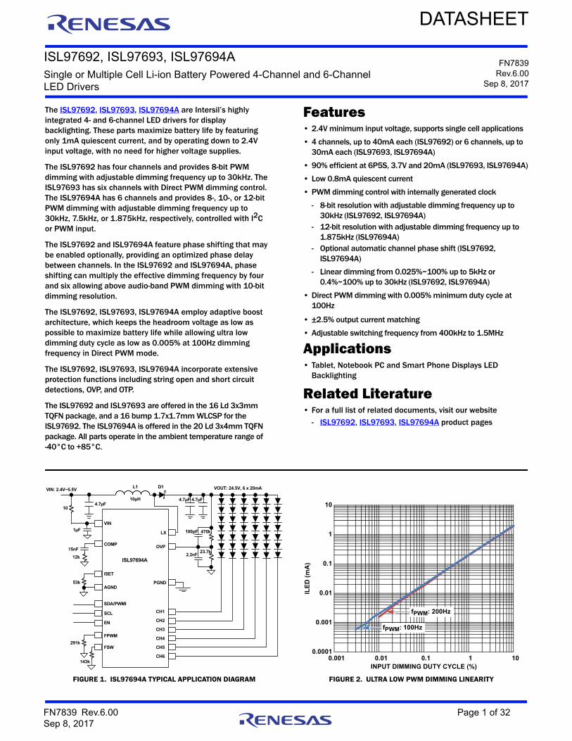
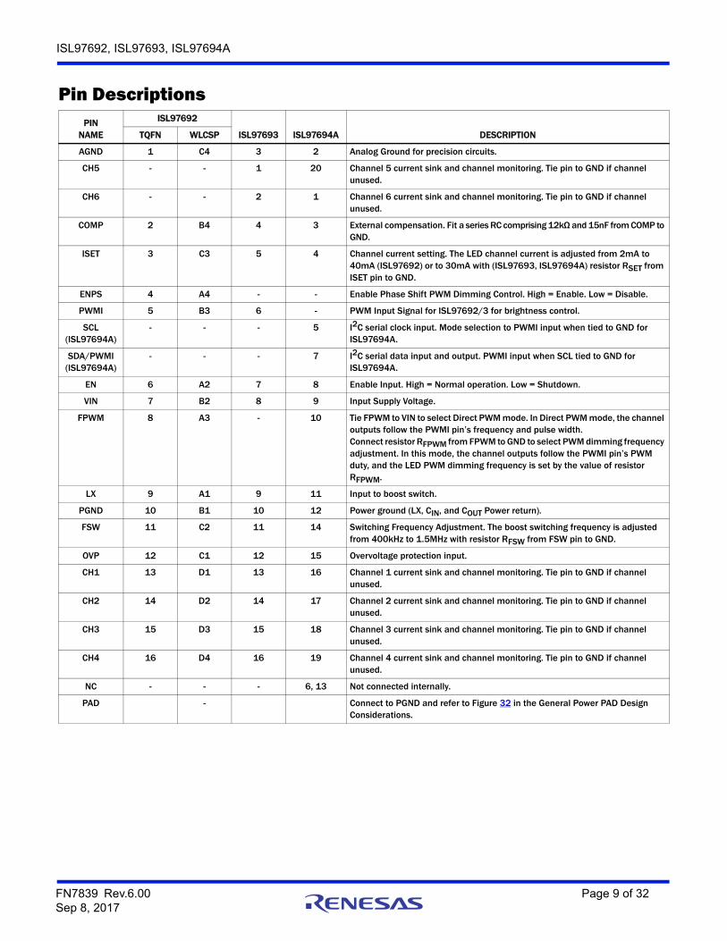
The ISL97692, ISL97693, ISL97694A are Intersil’s highly integrated 4- and 6-channel LED drivers for display backlighting. These parts maximize battery life by featuring only 1mA quiescent current, and by operating down to 2.4V input voltage, with no need for higher voltage supplies.
The ISL97692 has four channels and provides 8-bit PWM dimming with adjustable dimming frequency up to 30kHz. The ISL97693 has six channels with Direct PWM dimming control. The ISL97694A has 6 channels and provides 8-, 10-, or 12-bit PWM dimming with adjustable dimming frequency up to 30kHz, 7.5kHz, or 1.875kHz, respectively, controlled with I2C or PWM input.
The ISL97692 and ISL97694A feature phase shifting that may be enabled optionally, providing an optimized phase delay between channels. In the ISL97692 and ISL97694A, phase shifting can multiply the effective dimming frequency by four and six allowing above audio-band PWM dimming with 10-bit dimming resolution.
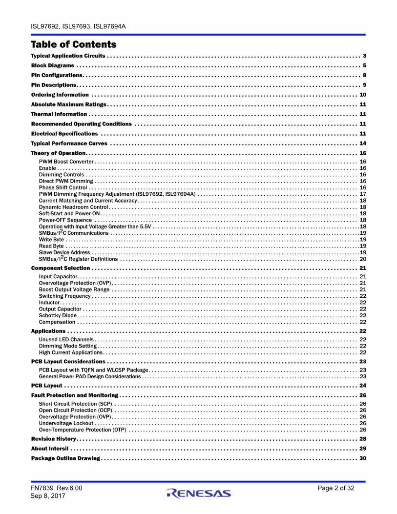
The ISL97692, ISL97693, ISL97694A employ adaptive boost architecture, which keeps the headroom voltage as low as possible to maximize battery life while allowing ultra low dimming duty cycle as low as 0.005% at 100Hz dimming frequency in Direct PWM mode.
The ISL97692, ISL97693, ISL97694A incorporate extensive protection functions including string open and short circuit detections, OVP, and OTP.
The ISL97692 and ISL97693 are offered in the 16 Ld 3x3mm TQFN package, and a 16 bump 1.7x1.7mm WLCSP for the ISL97692. The ISL97694A is offered in the 20 Ld 3x4mm TQFN package. All parts operate in the ambient temperature range of -40°C to +85°C.
Features• 2.4V minimum input voltage, supports single cell applications
• 4 channels, up to 40mA each (ISL97692) or 6 channels, up to 30mA each (ISL97693, ISL97694A)
• 90% efficient at 6P5S, 3.7V and 20mA (ISL97693, ISL97694A)
• Low 0.8mA quiescent current
• PWM dimming control with internally generated clock
- 8-bit resolution with adjustable dimming frequency up to 30kHz (ISL97692, ISL97694A)
- 12-bit resolution with adjustable dimming frequency up to 1.875kHz (ISL97694A)
- Optional automatic channel phase shift (ISL97692, ISL97694A)
- Linear dimming from 0.025%~100% up to 5kHz or 0.4%~100% up to 30kHz (ISL97692, ISL97694A)
• Direct PWM dimming with 0.005% minimum duty cycle at 100Hz
• ±2.5% output current matching
• Adjustable switching frequency from 400kHz to 1.5MHz
Applications• Tablet, Notebook PC and Smart Phone Displays LED
Backlighting
Related Literature• For a full list of related documents, visit our website
- ISL97692, ISL97693, ISL97694A product pages
FIGURE 1. ISL97694A TYPICAL APPLICATION DIAGRAM FIGURE 2. ULTRA LOW PWM DIMMING LINEARITY
FSW
FPWM
AGND
OVP
VIN
SDA/PWMI
ISET
COMP
SCL
D1
CH1
CH2
CH3
CH4
PGND
LX
VIN: 2.4V~5.5V VOUT: 24.5V, 6 x 20mA
CH5
CH6
L1
10µH
12k
15nF
10
1µF
4.7µF4.7µF
470k
23.7k
143k
291k
53k
100pF
2.2nFISL97694A
4.7µF
EN
0.0001
0.001
0.01
0.1
1
10
0.001 0.01 0.1 1 10INPUT DIMMING DUTY CYCLE (%)
ILE
D (
mA
)
fPWM: 200Hz
fPWM: 100Hz
FN7839 Rev.6.00 Page 1 of 32Sep 8, 2017
ISL97692, ISL97693, ISL97694A
Table of ContentsTypical Application Circuits . . . . . . . . . . . . . . . . . . . . . . . . . . . . . . . . . . . . . . . . . . . . . . . . . . . . . . . . . . . . . . . . . . . . . . . . . . . . . . . . . . . 3
Block Diagrams . . . . . . . . . . . . . . . . . . . . . . . . . . . . . . . . . . . . . . . . . . . . . . . . . . . . . . . . . . . . . . . . . . . . . . . . . . . . . . . . . . . . . . . . . . . . . 5
Pin Configurations. . . . . . . . . . . . . . . . . . . . . . . . . . . . . . . . . . . . . . . . . . . . . . . . . . . . . . . . . . . . . . . . . . . . . . . . . . . . . . . . . . . . . . . . . . . 8
Pin Descriptions. . . . . . . . . . . . . . . . . . . . . . . . . . . . . . . . . . . . . . . . . . . . . . . . . . . . . . . . . . . . . . . . . . . . . . . . . . . . . . . . . . . . . . . . . . . . . 9
Ordering Information . . . . . . . . . . . . . . . . . . . . . . . . . . . . . . . . . . . . . . . . . . . . . . . . . . . . . . . . . . . . . . . . . . . . . . . . . . . . . . . . . . . . . . . 10
Absolute Maximum Ratings . . . . . . . . . . . . . . . . . . . . . . . . . . . . . . . . . . . . . . . . . . . . . . . . . . . . . . . . . . . . . . . . . . . . . . . . . . . . . . . . . . 11
Thermal Information . . . . . . . . . . . . . . . . . . . . . . . . . . . . . . . . . . . . . . . . . . . . . . . . . . . . . . . . . . . . . . . . . . . . . . . . . . . . . . . . . . . . . . . . 11
Recommended Operating Conditions . . . . . . . . . . . . . . . . . . . . . . . . . . . . . . . . . . . . . . . . . . . . . . . . . . . . . . . . . . . . . . . . . . . . . . . . . 11
Electrical Specifications . . . . . . . . . . . . . . . . . . . . . . . . . . . . . . . . . . . . . . . . . . . . . . . . . . . . . . . . . . . . . . . . . . . . . . . . . . . . . . . . . . . . 11
Typical Performance Curves . . . . . . . . . . . . . . . . . . . . . . . . . . . . . . . . . . . . . . . . . . . . . . . . . . . . . . . . . . . . . . . . . . . . . . . . . . . . . . . . . 14
Theory of Operation. . . . . . . . . . . . . . . . . . . . . . . . . . . . . . . . . . . . . . . . . . . . . . . . . . . . . . . . . . . . . . . . . . . . . . . . . . . . . . . . . . . . . . . . . 16PWM Boost Converter . . . . . . . . . . . . . . . . . . . . . . . . . . . . . . . . . . . . . . . . . . . . . . . . . . . . . . . . . . . . . . . . . . . . . . . . . . . . . . . . . . . . . . . . . . . . 16Enable . . . . . . . . . . . . . . . . . . . . . . . . . . . . . . . . . . . . . . . . . . . . . . . . . . . . . . . . . . . . . . . . . . . . . . . . . . . . . . . . . . . . . . . . . . . . . . . . . . . . . . . . . 16Dimming Controls . . . . . . . . . . . . . . . . . . . . . . . . . . . . . . . . . . . . . . . . . . . . . . . . . . . . . . . . . . . . . . . . . . . . . . . . . . . . . . . . . . . . . . . . . . . . . . . 16Direct PWM Dimming . . . . . . . . . . . . . . . . . . . . . . . . . . . . . . . . . . . . . . . . . . . . . . . . . . . . . . . . . . . . . . . . . . . . . . . . . . . . . . . . . . . . . . . . . . . . 16Phase Shift Control . . . . . . . . . . . . . . . . . . . . . . . . . . . . . . . . . . . . . . . . . . . . . . . . . . . . . . . . . . . . . . . . . . . . . . . . . . . . . . . . . . . . . . . . . . . . . . 16PWM Dimming Frequency Adjustment (ISL97692, ISL97694A) . . . . . . . . . . . . . . . . . . . . . . . . . . . . . . . . . . . . . . . . . . . . . . . . . . . . . . . . 17Current Matching and Current Accuracy. . . . . . . . . . . . . . . . . . . . . . . . . . . . . . . . . . . . . . . . . . . . . . . . . . . . . . . . . . . . . . . . . . . . . . . . . . . . . 18Dynamic Headroom Control . . . . . . . . . . . . . . . . . . . . . . . . . . . . . . . . . . . . . . . . . . . . . . . . . . . . . . . . . . . . . . . . . . . . . . . . . . . . . . . . . . . . . . . 18Soft-Start and Power ON. . . . . . . . . . . . . . . . . . . . . . . . . . . . . . . . . . . . . . . . . . . . . . . . . . . . . . . . . . . . . . . . . . . . . . . . . . . . . . . . . . . . . . . . . . 18Power-OFF Sequence . . . . . . . . . . . . . . . . . . . . . . . . . . . . . . . . . . . . . . . . . . . . . . . . . . . . . . . . . . . . . . . . . . . . . . . . . . . . . . . . . . . . . . . . . . . . 18Operation with Input Voltage Greater than 5.5V . . . . . . . . . . . . . . . . . . . . . . . . . . . . . . . . . . . . . . . . . . . . . . . . . . . . . . . . . . . . . . . . . . . . . . . . . . . . . . .18SMBus/I2C Communications . . . . . . . . . . . . . . . . . . . . . . . . . . . . . . . . . . . . . . . . . . . . . . . . . . . . . . . . . . . . . . . . . . . . . . . . . . . . . . . . . . . . . . . . . . . . . . .19Write Byte . . . . . . . . . . . . . . . . . . . . . . . . . . . . . . . . . . . . . . . . . . . . . . . . . . . . . . . . . . . . . . . . . . . . . . . . . . . . . . . . . . . . . . . . . . . . . . . . . . . . . . . . . . . . . . . .19Read Byte . . . . . . . . . . . . . . . . . . . . . . . . . . . . . . . . . . . . . . . . . . . . . . . . . . . . . . . . . . . . . . . . . . . . . . . . . . . . . . . . . . . . . . . . . . . . . . . . . . . . . . . . . . . . . . . .19Slave Device Address . . . . . . . . . . . . . . . . . . . . . . . . . . . . . . . . . . . . . . . . . . . . . . . . . . . . . . . . . . . . . . . . . . . . . . . . . . . . . . . . . . . . . . . . . . . . . . . . . . . . . .19SMBus/I2C Register Definitions . . . . . . . . . . . . . . . . . . . . . . . . . . . . . . . . . . . . . . . . . . . . . . . . . . . . . . . . . . . . . . . . . . . . . . . . . . . . . . . . . . . 20
Component Selection . . . . . . . . . . . . . . . . . . . . . . . . . . . . . . . . . . . . . . . . . . . . . . . . . . . . . . . . . . . . . . . . . . . . . . . . . . . . . . . . . . . . . . . 21Input Capacitor. . . . . . . . . . . . . . . . . . . . . . . . . . . . . . . . . . . . . . . . . . . . . . . . . . . . . . . . . . . . . . . . . . . . . . . . . . . . . . . . . . . . . . . . . . . . . . . . . . 21Overvoltage Protection (OVP) . . . . . . . . . . . . . . . . . . . . . . . . . . . . . . . . . . . . . . . . . . . . . . . . . . . . . . . . . . . . . . . . . . . . . . . . . . . . . . . . . . . . . . 21Boost Output Voltage Range . . . . . . . . . . . . . . . . . . . . . . . . . . . . . . . . . . . . . . . . . . . . . . . . . . . . . . . . . . . . . . . . . . . . . . . . . . . . . . . . . . . . . . 21Switching Frequency . . . . . . . . . . . . . . . . . . . . . . . . . . . . . . . . . . . . . . . . . . . . . . . . . . . . . . . . . . . . . . . . . . . . . . . . . . . . . . . . . . . . . . . . . . . . . 22Inductor. . . . . . . . . . . . . . . . . . . . . . . . . . . . . . . . . . . . . . . . . . . . . . . . . . . . . . . . . . . . . . . . . . . . . . . . . . . . . . . . . . . . . . . . . . . . . . . . . . . . . . . . 22Output Capacitor . . . . . . . . . . . . . . . . . . . . . . . . . . . . . . . . . . . . . . . . . . . . . . . . . . . . . . . . . . . . . . . . . . . . . . . . . . . . . . . . . . . . . . . . . . . . . . . . 22Schottky Diode . . . . . . . . . . . . . . . . . . . . . . . . . . . . . . . . . . . . . . . . . . . . . . . . . . . . . . . . . . . . . . . . . . . . . . . . . . . . . . . . . . . . . . . . . . . . . . . . . . 22Compensation . . . . . . . . . . . . . . . . . . . . . . . . . . . . . . . . . . . . . . . . . . . . . . . . . . . . . . . . . . . . . . . . . . . . . . . . . . . . . . . . . . . . . . . . . . . . . . . . . . 22
Applications . . . . . . . . . . . . . . . . . . . . . . . . . . . . . . . . . . . . . . . . . . . . . . . . . . . . . . . . . . . . . . . . . . . . . . . . . . . . . . . . . . . . . . . . . . . . . . . 22Unused LED Channels . . . . . . . . . . . . . . . . . . . . . . . . . . . . . . . . . . . . . . . . . . . . . . . . . . . . . . . . . . . . . . . . . . . . . . . . . . . . . . . . . . . . . . . . . . . . 22Dimming Mode Setting . . . . . . . . . . . . . . . . . . . . . . . . . . . . . . . . . . . . . . . . . . . . . . . . . . . . . . . . . . . . . . . . . . . . . . . . . . . . . . . . . . . . . . . . . . . 22High Current Applications . . . . . . . . . . . . . . . . . . . . . . . . . . . . . . . . . . . . . . . . . . . . . . . . . . . . . . . . . . . . . . . . . . . . . . . . . . . . . . . . . . . . . . . . . 22
PCB Layout Considerations . . . . . . . . . . . . . . . . . . . . . . . . . . . . . . . . . . . . . . . . . . . . . . . . . . . . . . . . . . . . . . . . . . . . . . . . . . . . . . . . . . 23PCB Layout with TQFN and WLCSP Package . . . . . . . . . . . . . . . . . . . . . . . . . . . . . . . . . . . . . . . . . . . . . . . . . . . . . . . . . . . . . . . . . . . . . . . . . 23General Power PAD Design Considerations . . . . . . . . . . . . . . . . . . . . . . . . . . . . . . . . . . . . . . . . . . . . . . . . . . . . . . . . . . . . . . . . . . . . . . . . . . . . . . . . . . .23
PCB Layout . . . . . . . . . . . . . . . . . . . . . . . . . . . . . . . . . . . . . . . . . . . . . . . . . . . . . . . . . . . . . . . . . . . . . . . . . . . . . . . . . . . . . . . . . . . . . . . . 24
Fault Protection and Monitoring . . . . . . . . . . . . . . . . . . . . . . . . . . . . . . . . . . . . . . . . . . . . . . . . . . . . . . . . . . . . . . . . . . . . . . . . . . . . . . 26Short Circuit Protection (SCP) . . . . . . . . . . . . . . . . . . . . . . . . . . . . . . . . . . . . . . . . . . . . . . . . . . . . . . . . . . . . . . . . . . . . . . . . . . . . . . . . . . . . . 26Open Circuit Protection (OCP) . . . . . . . . . . . . . . . . . . . . . . . . . . . . . . . . . . . . . . . . . . . . . . . . . . . . . . . . . . . . . . . . . . . . . . . . . . . . . . . . . . . . . 26Overvoltage Protection (OVP) . . . . . . . . . . . . . . . . . . . . . . . . . . . . . . . . . . . . . . . . . . . . . . . . . . . . . . . . . . . . . . . . . . . . . . . . . . . . . . . . . . . . . . 26Undervoltage Lockout . . . . . . . . . . . . . . . . . . . . . . . . . . . . . . . . . . . . . . . . . . . . . . . . . . . . . . . . . . . . . . . . . . . . . . . . . . . . . . . . . . . . . . . . . . . . 26Over-Temperature Protection (OTP) . . . . . . . . . . . . . . . . . . . . . . . . . . . . . . . . . . . . . . . . . . . . . . . . . . . . . . . . . . . . . . . . . . . . . . . . . . . . . . . . 26
Revision History. . . . . . . . . . . . . . . . . . . . . . . . . . . . . . . . . . . . . . . . . . . . . . . . . . . . . . . . . . . . . . . . . . . . . . . . . . . . . . . . . . . . . . . . . . . . 28
About Intersil . . . . . . . . . . . . . . . . . . . . . . . . . . . . . . . . . . . . . . . . . . . . . . . . . . . . . . . . . . . . . . . . . . . . . . . . . . . . . . . . . . . . . . . . . . . . . . 29
Package Outline Drawing . . . . . . . . . . . . . . . . . . . . . . . . . . . . . . . . . . . . . . . . . . . . . . . . . . . . . . . . . . . . . . . . . . . . . . . . . . . . . . . . . . . . 30
FN7839 Rev.6.00 Page 2 of 32Sep 8, 2017

ISL97692, ISL97693, ISL97694A
Typical Application Circuits
FIGURE 3. ISL97692 TYPICAL APPLICATION DIAGRAM - 4P7S
FIGURE 4. ISL97693 TYPICAL APPLICATION DIAGRAM - 6P7S
FSW
FPWM
AGND
OVP
VIN
ENPS
ISET
COMP
PWMI
D1
CH1
CH2
CH3
CH4
PGND
LX
VIN: 2 .4V~5.5V VOUT: 24.5V, 4 x 20mAL1
10µH
12k
15nF
10
1µF
4.7µF4.7µF
470k
23.7k
143k
291k
53k
100pF
2.2nF
ISL97692
4.7µF
EN
FSW
AGND
OVP
VIN
PWMI
ISET
COMP
D1
CH1
CH2
CH3
CH4
PGND
LX
V IN: 2.4V~5.5V VOUT: 24.5V, 6 x 20mA
CH5
CH6
L1
10µH
12k
15nF
10
1µF
4.7µF4.7µF
470k
23.7k
143k
53k
100pF
2.2nFISL97693
4.7µF
EN
FN7839 Rev.6.00 Page 3 of 32Sep 8, 2017

ISL97692, ISL97693, ISL97694A
FIGURE 5. ISL97694A TYPICAL APPLICATION DIAGRAM- 6P7S
Typical Application Circuits (Continued)
FSW
FPWM
AGND
OVP
VIN
SDA/PWMI
ISET
COMP
SCL
D1
CH1
CH2
CH3
CH4
PGND
LX
VIN: 2 .4V~5.5V VOUT: 24.5V, 6 x 20mA
CH5
CH6
L1
10µH
12k
15nF
10
1µF
4.7µF4.7µF
470k
23.7k
143k
291k
53k
100pF
2.2nFISL97694A
4.7µF
EN
FN7839 Rev.6.00 Page 4 of 32Sep 8, 2017
ISL97692, ISL97693, ISL97694A
Block Diagrams
FIGURE 6. ISL97692 BLOCK DIAGRAM
REFGEN
VIN
GMAMP
COMP
+-
CH1
CH4
PWM/PFM
LOGIC
FETDRIVERS
OVPREG
OSC & RAMP COMP
IMAX ILIMIT
HIGHEST VF
STRING DETECT
TEMPSENSORENPS
ISET
+-
O/P SHORT
REF_OVP REF_VSC
INTERNAL BIAS
+-
OPEN CKT, SHORT CKT DETECTION
1
DYNAMIC HEADROOM CONTROL
OVP
4
FSW
PWMI
PHASESHIFT & PWM
DIMMING CONTROLLER
2
3
24V, 4x40mA
LX
VIN: 2.4V TO 5.5V
FPWM
OPTIONAL FUSE
8-BITDIGITIZER
DIRECT PWM
DETECT
10µH
EN
8-BIT DAC
ISL97692
CH2CH3
PGND
FN7839 Rev.6.00 Page 5 of 32Sep 8, 2017

ISL97692, ISL97693, ISL97694A
FIGURE 7. ISL97693 BLOCK DIAGRAM
Block Diagrams (Continued)
REFGEN
VIN
GMAMP
COMP
+-
CH1
CH4
PWM/PFM
LOGIC
FETDRIVERS
OVPREG
OSC & RAMP COMP
IMAX ILIMIT
HIGHEST VF
STRING DETECT
TEMPSENSOR
ISET
+-
O/P SHORT
REF_OVP REF_VSC
INTERNAL BIAS
+-
OPEN CKT, SHORT CKT DETECTION
1
DYNAMIC HEADROOM CONTROL
OVP
6
FSW
PWM DIMMING
CONTROLLER
2
3
24V, 6x30mA
LX
VIN: 2.4V TO 5.5V
OPTIONAL FUSE 10µH
EN
8-BIT DAC
PGND
ISL97693
CH2CH3
4
5
CH6
CH5
PWMI
FN7839 Rev.6.00 Page 6 of 32Sep 8, 2017

ISL97692, ISL97693, ISL97694A
FIGURE 8. ISL97694A BLOCK DIAGRAM
Block Diagrams (Continued)
REF
GEN
VIN
GMAMP
COMP
+-
CH1
CH4
PWM/PFM
LOGIC
FETDRIVERS
OVPREG
OSC & RAMP COMP
IMAX ILIMIT
HIGHEST VF
STRING DETECT
TEMPSENSOR
ISET
+-
O/P SHORT
REF_OVP REF_VSC
INTERNAL BIAS
+-
OPEN CKT, SHORT CKT DETECTION
1
DYNAMIC HEADROOM CONTROL
OVP
6
FSW
SCL
PHASESHIFT & PWM
DIMMING CONTROLLER
2
3
24V, 6x30mA
LX
VIN: 2.4V TO 5.5V
FPWM
OPTIONAL FUSE
I2CCONTROLLER
DIRECT PWM
DETECT
10µH
EN
8-BIT DAC
PGND
ISL97694A
CH2CH3
4
5
CH6
CH5
SDA/PWMI
FN7839 Rev.6.00 Page 7 of 32Sep 8, 2017

ISL97692, ISL97693, ISL97694A
s
Pin ConfigurationsISL97692
(16 LD TQFN)TOP VIEW
ISL97692(1.7x1.7x0.53mm, 16 BALL, 0.4mm PITCH WLCSP)
TOP VIEW
ISL97693 (16 LD TQFN)
TOP VIEW
ISL97694A(20 LD TQFN)
TOP VIEW
1
2
3
4
12
11
10
9
5 6 7 8
16 15 14
13
AGND
COMP
ISET
ENPS
PW
MI
EN
VIN
FP
WM
CH
4
CH
3
CH
2
CH
1
OVP
FSW
PGND
LX
Thermal PAD
A
C
B
2
D
4 3 1
CH4 CH3 CH2 CH1
AGND
COMP
ENPS
ISET
PWMI
EN
VIN
LX
PGND
OVPFSW
FPWM
1
2
3
4
12
11
10
9
5 6 7 8
16
15 14
13
CH5
CH6
AGND
COMP
ISE
T
PW
MI
EN
VIN
CH
4
CH
3
CH
2
CH
1
OVP
FSW
PGND
LX
Thermal PAD
SD
A/P
WM
I
ISET
PGND
NC
EN
VIN
CH
4
CH
5
CH
3
FP
WM
OVPAGND
FSW
CH
2
CH6
COMP
SCL
LX
1
2
3
4
5
7 8 9 10
15
14
13
12
11
20 19 18 17
6NC
6 CH116
Thermal PAD
FN7839 Rev.6.00 Page 8 of 32Sep 8, 2017
ISL97692, ISL97693, ISL97694A
Pin DescriptionsPIN
NAME
ISL97692
ISL97693 ISL97694A DESCRIPTIONTQFN WLCSP
AGND 1 C4 3 2 Analog Ground for precision circuits.
CH5 - - 1 20 Channel 5 current sink and channel monitoring. Tie pin to GND if channel unused.
CH6 - - 2 1 Channel 6 current sink and channel monitoring. Tie pin to GND if channel unused.
COMP 2 B4 4 3 External compensation. Fit a series RC comprising 12kΩ and 15nF from COMP to GND.
ISET 3 C3 5 4 Channel current setting. The LED channel current is adjusted from 2mA to 40mA (ISL97692) or to 30mA with (ISL97693, ISL97694A) resistor RSET from ISET pin to GND.
ENPS 4 A4 - - Enable Phase Shift PWM Dimming Control. High = Enable. Low = Disable.
PWMI 5 B3 6 - PWM Input Signal for ISL97692/3 for brightness control.
SCL(ISL97694A)
- - - 5 I2C serial clock input. Mode selection to PWMI input when tied to GND for ISL97694A.
SDA/PWMI(ISL97694A)
- - - 7 I2C serial data input and output. PWMI input when SCL tied to GND for ISL97694A.
EN 6 A2 7 8 Enable Input. High = Normal operation. Low = Shutdown.
VIN 7 B2 8 9 Input Supply Voltage.
FPWM 8 A3 - 10 Tie FPWM to VIN to select Direct PWM mode. In Direct PWM mode, the channel outputs follow the PWMI pin’s frequency and pulse width. Connect resistor RFPWM from FPWM to GND to select PWM dimming frequency adjustment. In this mode, the channel outputs follow the PWMI pin’s PWM duty, and the LED PWM dimming frequency is set by the value of resistor RFPWM.
LX 9 A1 9 11 Input to boost switch.
PGND 10 B1 10 12 Power ground (LX, CIN, and COUT Power return).
FSW 11 C2 11 14 Switching Frequency Adjustment. The boost switching frequency is adjusted from 400kHz to 1.5MHz with resistor RFSW from FSW pin to GND.
OVP 12 C1 12 15 Overvoltage protection input.
CH1 13 D1 13 16 Channel 1 current sink and channel monitoring. Tie pin to GND if channel unused.
CH2 14 D2 14 17 Channel 2 current sink and channel monitoring. Tie pin to GND if channel unused.
CH3 15 D3 15 18 Channel 3 current sink and channel monitoring. Tie pin to GND if channel unused.
CH4 16 D4 16 19 Channel 4 current sink and channel monitoring. Tie pin to GND if channel unused.
NC - - - 6, 13 Not connected internally.
PAD - Connect to PGND and refer to Figure 32 in the General Power PAD Design Considerations.
FN7839 Rev.6.00 Page 9 of 32Sep 8, 2017

ISL97692, ISL97693, ISL97694A
Ordering InformationPART NUMBER
(Note 5)PART
MARKINGTEMP RANGE
(°C)PACKAGE
(RoHS CompliantPKG.
DWG. #
ISL97692IRTZ (Notes 1, 3) 7692 -40 to +85 16 Ld 3x3x0.75mm TQFN L16.3x3D
ISL97692IIZ-T (Notes 2, 4) 7692 -40 to +85 16 Bump 1.7x1.7mm, 0.4mm Pitch WLCSP W4x4.16B
ISL97693IRTZ (Notes 1, 3) 7693 -40 to +85 16 Ld 3x3x0.75mm TQFN L16.3x3D
ISL97694AIRTZ (Notes 1, 3) 694A -40 to +85 20 Ld 3x4x0.8mm TQFN L20.3x4A
NOTES:
1. Add “-T” suffix for for 6k unit or “-TK” suffix for 1k unit tape and reel options. Refer to TB347 for details on reel specifications.
2. Add “-T” suffix for for 3k unit tape and reel option. Refer to TB347 for details on reel specifications.
3. These Intersil Pb-free plastic packaged products employ special Pb-free material sets, molding compounds/die attach materials, and 100% matte tin plate plus anneal (e3 termination finish, which is RoHS compliant and compatible with both SnPb and Pb-free soldering operations). Intersil Pb-free products are MSL classified at Pb-free peak reflow temperatures that meet or exceed the Pb-free requirements of IPC/JEDEC J STD-020.
4. These Intersil Pb-free WLCSP packaged products employ special Pb-free material sets; molding compounds/die attach materials and SnAgCu - e1 solder ball terminals, which are RoHS compliant and compatible with both SnPb and Pb-free soldering operations. Intersil Pb-free WLCSP packaged products are MSL classified at Pb-free peak reflow temperatures that meet or exceed the Pb-free requirements of IPC/JEDEC J STD-020.
5. For Moisture Sensitivity Level (MSL), see the product information page for ISL97692, ISL97693, ISL97694A. For more information on MSL, see TB363.
FN7839 Rev.6.00 Page 10 of 32Sep 8, 2017

ISL97692, ISL97693, ISL97694A
Absolute Maximum Ratings (Note 6) Thermal InformationVIN, ISET, COMP, OVP . . . . . . . . . . . . . . . . . . . . . . . . . . . . . . . . . . . -0.3V to 6VPWMI, FPWM, FSW . . . . . . . . . . . . . . . . . . . . . . . . . . . . . . . . . . . . -0.3V to 6VEN, ENPS, SCL, SDA/PWMI . . . . . . . . . . . . . . . . . . . . . . . . . . . . . . -0.3V to 6VCH1 to CH6, LX . . . . . . . . . . . . . . . . . . . . . . . . . . . . . . . . . . . . . . . -0.3V to 28VPGND, AGND . . . . . . . . . . . . . . . . . . . . . . . . . . . . . . . . . . . . . . . -0.3V to +0.3VMaximum Average Current Into LX Pin for TQFN . . . . . . . . . . . . . . . . . .2.6A Maximum Average Current Into LX Pin for CSP . . . . . . . . . . . . . . . . . . . . 1A ESD Ratings
Human Body Model (Tested per JESD22-A114F) (ISL97692, ISL97693) . . . . . . . . . . . . . . . . . . . . . . . . . . . . . . . . . . . . 2kV
Human Body Model (Tested per JESD22-A114F) (ISL97694A) . . .2.5kVMachine Model (Tested per JESD22-A115C) . . . . . . . . . . . . . . . . . . 200VCharged Device Model (JESD22-C101E) . . . . . . . . . . . . . . . . . . . . . . . 2kV
Latch-Up (Tested per JESD-78B; Class 2, Level A) . . . . . . . . . . . . . . 100mA
Recommended Operating ConditionsInput Voltage (VIN) . . . . . . . . . . . . . . . . . . . . . . . . . . . . . . . . . . . . 2.4V to 5.5VOutput Voltage (VOUT) . . . . . . . . . . . . . . . . . . . . . . . . . . . . . . . . . . .Up to 26V Ambient Temperature Range . . . . . . . . . . . . . . . . . . . . . . . . -40°C to +85°C
Thermal Resistance (Typical) JA (°C/W) JC (°C/W)16 Ld TQFN (Notes 7, 8) . . . . . . . . . . . . . . . 51 4.620 Ld TQFN (Notes 7, 8) . . . . . . . . . . . . . . . 45 3.016 Bump WLCSP (Note 7) . . . . . . . . . . . . . . 82 N/A
Thermal Characterization (Typical) (Note 9) PSIJT (°C/W)
16 Ld TQFN . . . . . . . . . . . . . . . . . . . . . . . . . . . . . . . . . . . . 0.1120 Ld TQFN . . . . . . . . . . . . . . . . . . . . . . . . . . . . . . . . . . . . 0.1
Thermal Characterization (Typical) PSIJB (°C/W)
16 Bump WLCSP (Note 10). . . . . . . . . . . . . . . . . . . . . . . 22Maximum Continuous Junction Temperature . . . . . . . . . . . . . . . . .+125°CStorage Temperature . . . . . . . . . . . . . . . . . . . . . . . . . . . . .-65°C to +150°CPb-Free Reflow Profile . . . . . . . . . . . . . . . . . . . . . . . . . . . . . . . . . . see TB493
CAUTION: Do not operate at or near the maximum ratings listed for extended periods of time. Exposure to such conditions may adversely impact productreliability and result in failures not covered by warranty.
NOTES:
6. Voltage Ratings are all with respect to the AGND pin.
7. JA is measured in free air with the component mounted on a high-effective thermal conductivity test board with “direct attach” features. See TB379.
8. For JC, the “case temp” location is the center of the exposed metal pad on the package underside.
9. PSIJT is the PSI junction-to-top thermal characterization parameter. If the package top temperature can be measured with this rating then the die junction temperature can be estimated more accurately than the JC and JC thermal resistance ratings.
10. PSIJB is the PSI junction-to-board thermal characterization parameter.
Electrical Specifications VIN = EN = 3.3V, TA = +25°C unless otherwise noted. Boldface limits apply over the operating temperature range, -40°C to +85°C.
PARAMETER DESCRIPTION CONDITIONMIN
(Note 11) TYPMAX
(Note 11) UNIT
GENERAL
VIN Backlight Supply Voltage, (Notes 12, 13) TA = +25°C 2.4 5.5 V
IVIN_Standby Standby current EN = Low, LDO disabled 1 µA
IVIN VIN Active Current, ILED = 40mA (ISL97692) 30mA (ISL97693/(ISL97694A)
All channels 100% duty 2.5 mA
All channels 0% duty 0.8 mA
VOUT Output Voltage VIN ≥ 2.7V, ILED = 40mA (ISL97692) 30mA (ISL97693/4A)
26 V
VUVLO Undervoltage Lockout Threshold 2 2.15 2.35 V
VUVLO_HYS Undervoltage Lockout Hysteresis 150 mV
ENLow EN Input Low Voltage 0.5 V
ENHi EN Input High Voltage 1.5 V
BOOST SWITCHING REGULATOR
SS Soft-start 100% LED Duty Cycle 7 ms
SWILimit Boost FET Current Limit for QFN 2.7V < VIN < 5.5V, fSW = 600kHz, L = 10µH, TA ≤ +55°C
2.45 2.8 3.2 A
Boost FET Current Limit for CSP 1.2A 1.6A A
rDS(ON) Internal Boost Switch ON-Resistance TA = +25°C 212 mΩ
FN7839 Rev.6.00 Page 11 of 32Sep 8, 2017

ISL97692, ISL97693, ISL97694A
Eff_peak Peak Efficiency VIN = 5.5V, VOUT = 21V, TA = +25°C, RFSW = 144kΩ, ICH1-CH6 = 20mA,L = 10µH with DCR 150mΩ
90 %
VIN = 2.7V, VOUT = 21V, TA = +25°C, RFSW = 144kΩ, ICH1-CH6 = 20mA,L = 10µH with DCR 150mΩ
76 %
DMAX Boost Maximum Duty Cycle FSW = 400kHz 93.5 %
FSW = 1.5MHz 93 %
DMIN Boost Minimum Duty Cycle FSW = 400kHz 11 %
FSW = 1.5MHz 15 %
fSW Boost Switching Frequency RFSW = 216kΩ 360 400 440 kHz
RFSW = 72.1kΩ 1.2 MHz
RFSW = 57.7kΩ 1.35 1.5 1.65 MHz
ILX_leakage LX Leakage Current LX = 26V 10 µA
REFERENCE
IMATCH Channel-to-Channel DC Current Matching ILED = 20mA -2.5 +2.5 %
IACC Current Accuracy ILED = 20mA -3 +3 %
FAULT DETECTION
VSC Channel Short Circuit Threshold 6.75 8 9.25 V
Vtemp Over-Temperature Threshold 150 °C
VOVPlo Overvoltage Limit on OVP Pin 1.180 1.22 1.245 V
OVPfault OVP Short Detection Fault Level 75 mV
CURRENT SOURCES
Vheadroom Dominant Channel Current Source Headroom at CH Pin
ILED = 20mATA = +25°C
300(Note 14)
mV
VHEADROOM_RANGE Dominant Channel Current Sink Headroom Range at CHx Pin
ILED = 20mA,TA = +25°C
65 mV
ILED(max) Maximum LED Current per Channel 2.7V < VIN < 5.5V, VOUT = 21V(ISL97692 QFN)
40 mA
2.7V < VIN < 5.5V, VOUT = 21V (ISL97692 WLCSP, ISL97693, and ISL97694A)
30 mA
PWM GENERATOR
VIL Guaranteed Range for PWM Input Low Voltage
0.5 V
VIH Guaranteed Range for PWM Input High Voltage
1.5 V
FPWMI PWMI Input and Output Frequency Range
8-bit Dimming Resolution 100 30,000 Hz
10-bit Dimming Resolution 100 7.5 kHz
12-bit Dimming Resolution 100 1.87 kHz
DPWMACC Direct PWM Dimming Output Resolution (ISL97692, ISL97693 and ISL97694A) 80 ns
tDPWM_ON_MIN Direct PWM Dimming Minimum On-Time (ISL97692, ISL97693 and ISL97694A) 350 ns
PWMACCPWM Dimming with Adjustable Dimming Frequency Output Resolution
(ISL97692, ISL97694A) 8 bit
ISL97694A, En10Bit = 1 10 bit
ISL97694A, En12Bit = 1 12 bit
Electrical Specifications VIN = EN = 3.3V, TA = +25°C unless otherwise noted. Boldface limits apply over the operating temperature range, -40°C to +85°C. (Continued)
PARAMETER DESCRIPTION CONDITIONMIN
(Note 11) TYPMAX
(Note 11) UNIT
FN7839 Rev.6.00 Page 12 of 32Sep 8, 2017

ISL97692, ISL97693, ISL97694A
FPWM Generated PWM Dimming Frequency Range (ISL97692, ISL97694A) 100 30,000 Hz
SMBus/I2C INTERFACE (ISL97694A only)
VIL Guaranteed Range for Data, Clock Input Low Voltage
0.5 V
VIH Guaranteed Range for Data, Clock Input High Voltage
1.5 VDD V
VOL SMBus/I2C Output Data Line Logic Low Voltage
IPULLUP = 4mA 0.17 V
ILEAK Input Leakage On SDA/SCL Measured at 4.8V -10 10 µA
SMBus/I2C TIMING SPECIFICATIONS (ISL97694A only)
tEN-SMBus/I2C Minimum Time between VIN>UVLO and SMBus/I2C Enabled
2 ms
FSCL SCL Clock Frequency 400 kHz
tBUF Bus Free Time Between Stop and Start Condition
1.3 µs
tHD:STA Hold Time After (Repeated) START Condition After this Period, the First Clock is Generated
0.6 µs
tSU:STA Repeated Start Condition Setup Time 0.6 µs
tSU:STO Stop Condition Setup Time 0.6 µs
tHD:DAT Data Hold Time 300 ns
tSU:DAT Data Setup Time 100 ns
tHIGH Low Period of SCL Clock 1.3 µs
tLOW High Period of SCL Clock 0.6 µs
tF Clock/data Fall Time 300 ns
tR Clock/data Rise Time 300 ns
NOTES:
11. Parameters with MIN and/or MAX limits are 100% tested at +25°C, unless otherwise specified. Temperature limits established by characterization and are not production tested.
12. At maximum VIN of 5.5V, minimum VOUT is 6V. Minimum VOUT can be lower at lower VIN.
13. Limits established by characterization and are not production tested.
14. Varies within the range specified by VHEADROOM_RANGE.
Electrical Specifications VIN = EN = 3.3V, TA = +25°C unless otherwise noted. Boldface limits apply over the operating temperature range, -40°C to +85°C. (Continued)
PARAMETER DESCRIPTION CONDITIONMIN
(Note 11) TYPMAX
(Note 11) UNIT
FN7839 Rev.6.00 Page 13 of 32Sep 8, 2017
ISL97692, ISL97693, ISL97694A
Typical Performance Curves
FIGURE 9. EFFICIENCY vs VIN (ICH: 20mA, fDIM: 200Hz, FOR LEDs: 6P5S, 6P6S, 6P7S)
FIGURE 10. EFFICIENCY vs PWM DIMMING (VIN: 3.7V, ICH: 20mA, fDIM: 200Hz, FOR LEDs: 6P5S, 6P6S, 6P7S)
FIGURE 11. PWM DIMMING LINEARITY (VIN: 3.7V, VOUT: 21V FOR 6P7S, fDIM: 200Hz)
FIGURE 12. CHANNEL MATCHING ACCURACY (VIN: 3.7V, VOUT: 21V FOR 6P7S, ICH: 20mA)
FIGURE 13. START-UP (100% DIRECT PWM DIMMING, VIN: 3.7V, ICH: 20mA, LEDs: 6P7S, fDIM: 200Hz)
FIGURE 14. START-UP (100% DECODED PWM DIMMING, VIN: 3.7V, ICH: 20mA, LEDs: 6P7S, fDIM: 200Hz)
76
78
80
82
84
86
88
90
92
2.7 3.2 3.7 4.2 4.7 5.2
INPUT VOLTAGE (V)
EF
FIC
IEN
CY
(%
)
6P7S LEDs
6P6S LEDs
6P5S LEDs
PWM DIMMING (%)
EF
FIC
IEN
CY
(%
)
50
55
60
65
70
75
80
85
90
95
0 20 40 60 80 100
6P7S LEDs
6P5S LEDs
6P6S LEDs
0
5
10
15
20
0 20 40 60 80 100
INPUT DIMMING DUTY CYCLE (%)
LE
D C
UR
RE
NT
(m
A)
-2.5
-1.5
-0.5
0.5
1.5
2.5
0 1 2 3 4 5 6 7
CHANNEL NUMBER
MA
TC
HIN
G A
CC
UR
AC
Y (
%)
IC#1
IC#2
IC#3
IL
VOUT
VLX
VCH
IL
VOUT
VLX
VCH
FN7839 Rev.6.00 Page 14 of 32Sep 8, 2017

ISL97692, ISL97693, ISL97694A
FIGURE 15. START-UP (50% DIRECT PWM DIMMING, VIN: 3.7V, ICH: 20mA, LEDs: 6P7S, fDIM: 200Hz)
FIGURE 16. START-UP (50% DECODED PWM DIMMING, VIN: 3.7V, ICH: 20mA, LEDs: 6P7S, fDIM: 200Hz)
FIGURE 17. MINIMUM DIMMING DUTY CYCLE(0.003% DIRECT PWM DIMMING MODE, fDIM: 100Hz)
FIGURE 18. I2C CONTROL TIMING AND CHANNEL CURRENT (100% DIMMING, ISL97694A)
FIGURE 19. DECODED PWM DIMMING WITH PHASE SHIFT (VIN: 3.7V, ICH: 20mA, DIM: 17%, fDIM: 250Hz, LEDs: 6P6S)
FIGURE 20. DIRECT PWM DIMMING WITHOUT PHASE SHIFT(VIN: 3.7V, ICH: 20mA, DIM: 17%, fDIM: 250Hz, LEDs: 6P6S)
Typical Performance Curves (Continued)
IL
VOUT
VLX
VCH
IL
VOUT
VLX
VCH
ICH
PWM INPUT
S:Start P:Stop
SCL
SDA
I_CH
Slave address:01011010
R/W A
Brightness(100%): 11111111Command code (8bit)
AA
V_LX
I_L
V_CH1
V_CH2
IL
VCH1
VLX
VCH2
VLX
IL
VCH2
VCH1
FN7839 Rev.6.00 Page 15 of 32Sep 8, 2017

ISL97692, ISL97693, ISL97694A
Theory of OperationPWM Boost ConverterThe current mode PWM boost converter produces the minimal voltage needed to enable the LED stack with the highest forward voltage drop to run at the programmed current. The ISL97692, ISL97693, ISL97694A employs current mode control boost architecture that has a fast current sense loop and a slow voltage feedback loop. This architecture achieves the fast transient response, which is essential for portable product backlight applications where the backlight must not flicker when the power source is changed from a drained battery to an AC/DC adapter.
The number of LEDs that can be driven by ISL97692, ISL97693, ISL97694A depends on the type of LED chosen in the application. The maximum output is 26V at 40mA from 2.7V input.
EnableTake the EN input high to enable the ISL97692, ISL97693, ISL97694A for normal operation and low to enter low-power shutdown, which immediately turns off LED channels and the boost regulator.
Dimming ControlsThe ISL97692, ISL97693, ISL97694A allows the LED current to be programmed in the range 2mA to 40mA (ISL97692) or 2mA to 30mA (ISL97693, ISL97694A) by RSET per Equation 1:
Where:
- 1066 is a constant determined by design
- RSET is the resistor from ISET pin to GND (Ω)
- ILEDmax is the peak current set by resistor RSET (A)
For example, if the required LED current (ILEDmax) is 40mA, then the RSET value needed is:
Choose the nearest standard resistor: 26.65kΩ, 0.1%
Direct PWM DimmingThe ISL97693 always operates in Direct PWM dimming mode. The ISL97692 and ISL97694A can be selected to operate in Direct PWM dimming mode by connecting the FPWM pin to VIN and the SCL pin of ISL97694A must be tied to GND.
With Direct PWM, the channel outputs follow the input PWM signal frequency and pulse width, as provided to the PWMI pin. When PWMI is high, all channels sink the current set by the RSET resistor. When PWMI is low, all channels are high-Z.
The maximum allowed input PWM frequency at PWMI is 30kHz. The minimum duty is calculated by Equation 3 according to the input PWM frequency, and is set by the minimum channel on-time of 350ns.
For example, for a 200Hz input PWM frequency, the minimum duty cycle is:
The resolution is calculated by Equation 5 according to the input PWM frequency, and the fixed 80ns resolution of ISL97692, ISL97693, ISL97694A.
Thus the effective resolution at 200Hz is 15.9 bits:
Phase Shift ControlThe ISL97692, ISL97694A are capable of delaying the phase of each current source. Conventional LED drivers exhibit the worst load transients to the boost circuit by turning on all channels simultaneously, as shown in Figures 21 and 23. In contrast, the ISL97692, ISL97694A phase shift each channel by turning them on once during each PWM dimming period, as shown in Figures 22 and 24. At each dimming duty cycle (except at 100%) the sum of the phase shifted total current will be less than a conventional LED drivers’ total current.
For the ISL97692, ISL97694A, the channels are separated by 360°/N, where N is number of channels enabled. For example, if three channels are enabled, they will be separated by 120°.
If the channels are combined for higher current application, the phase shift function must be disabled by connecting the ENPS pin to ground.
ILEDmax1066RSET---------------= (EQ. 1)
RSET 1066 0.04 26.65k= = (EQ. 2)
(EQ. 3)Min Duty Cycle 350ns Input PWM Frequency=
(EQ. 4)Min Duty Cycle 350ns 200Hz 0.007%= =
(EQ. 5)PWM Resolution1
80ns Input PWM Frequency-------------------------------------------------------------------------------=
(EQ. 6)PWM Resolution1
80ns 200Hz-------------------------------------- 62500 15.9bits===
FIGURE 21. CONVENTIONAL 4-CH LED DRIVER WITH 10% PWM DIMMING CHANNEL CURRENT (UPPER) AND TOTAL CURRENT (LOWER)
ILED1-20mA
ILED_Total_80mA
TIME (ms)
ILED2-20mA
ILED3-20mA
ILED4-20mA
5 10 15
FN7839 Rev.6.00 Page 16 of 32Sep 8, 2017

ISL97692, ISL97693, ISL97694A
PWM Dimming Frequency Adjustment (ISL97692, ISL97694A)The ISL97692 and ISL97694A can use an internal oscillator to generate the PWM dimming frequency. In this mode, the duty of the signal at PWMI pin is measured with 8-, 10- or 12-bit resolution, and applied to the internally generated PWM dimming frequency. The dimming frequency is set by an external resistor RFPWM at the FPWM pin for ISL97692 and ISL97694A, per Equation 7:
Where:- R0 is determined by design
- R0 = 58.1 X 10⁶ for 8-bit
- R0 = 14.5 X 10⁶ for 10-bit
- R0 = 36.2 X 10⁵ for 12-bit
- FPWM is the required PWM dimming frequency (Hz)
- RFPWM is the resistor from FPWM pin to GND (Ω)
For example, to set the PWM dimming frequency to 480Hz at 8-bit resolution:
The maximum allowed input and output PWM dimming frequency varies according to the PWM resolution, per Table 1. This is configurable for the ISL97694A by the En12Bit and En10Bit bits in register 0x01.
FIGURE 22. ISL97692 PHASE SHIFT 4-CHANNELS LED DRIVER WITH 10% PWM DIMMING CHANNEL CURRENT (UPPER) AND TOTAL CURRENT (LOWER)
ILED1-20mA
ILED_Total_20mA
TIME (ms)
ILED2-20mA
ILED3-20mA
ILED4-20mA
5 10
FIGURE 23. CONVENTIONAL LED DRIVER PWM DIMMING CHANNEL AND TOTAL CURRENT AT 50% DUTY CYCLE
ILED4-20mA
ILED_Total_80mA
TIME (ms)
ILED3-20mA
ILED2-20mA
ILED1-20mA
5 10
FIGURE 24. ISL97692 PHASE SHIFT LED DRIVER PWM DIMMING CHANNEL AT 50% DUTY CYCLE
ILED4-20mA
ILED_Total_40mA
TIME (ms)
ILED3-20mA
ILED2-20mA
ILED1-20mA
5 10 TABLE 1. MAX PWM DIMMING FREQUENCY SET BY RFPWM
PARTMAX FREQUENCY
(kHz)PWM RESOLUTION
(BIT MODE)
ISL97692 30 8
ISL97694A
30 8
7.5 10
1.875 12
FIGURE 25. ISL97692 4 -CHANNELS PHASE SHIFT TIMING ILLUSTRATION
ILED1
ILED2
ILED3
ILED4
ILED1
tON
PWMI 60% 40%
60% 40%
tPWMIN
tFPWM (tPWMOUT)
tOFF
RFPWMR0
FPWM-----------------= (EQ. 7)
RFPWM58.1
610480
------------------------ 121k== (EQ. 8)
FN7839 Rev.6.00 Page 17 of 32Sep 8, 2017

ISL97692, ISL97693, ISL97694A
Current Matching and Current AccuracyEach channel of the LED current is regulated by a current sink circuit.
The LED peak current is set by the external RSET resistor according to Equation 1. The current sink MOSFETs in each LED driver channel output are designed to operate within a range at about 300mV to optimize power loss versus accuracy requirements. The sources of errors of the channel-to-channel current matching come from internal amplifier offsets, internal layout and reference accuracy. These parameters are optimized for current matching and absolute current accuracy. Absolute accuracy is also determined by the external resistor RSET, and so a 0.1% tolerance resistor is recommended.
Dynamic Headroom ControlThe ISL97692, ISL97693, ISL97694A features a proprietary Dynamic Headroom Control circuit that detects the highest forward voltage string or effectively the lowest voltage on any of the channel pins. When this lowest channel voltage is lower than the short circuit threshold, VSC, such voltage will be used as the feedback signal for the boost regulator. The boost makes the output to the correct level, such that the lowest channel pin is at the target headroom voltage. Since all LED stacks are connected to the same output voltage, the other channel pins will have a higher voltage, but the regulated current source circuit on each channel will ensure that each channel has the same current. The output voltage will regulate cycle-by-cycle and it is always referenced to the highest forward voltage string in the architecture.
Soft-Start and Power ONOnce the ISL97692, ISL97693, ISL97694A are powered up and the EN pin is taken high, the boost regulator will begin to switch and the current in the inductor will ramp-up. The current in the boost power switch is monitored and the switching is terminated in any cycle where the current exceeds the current limit. The ISL97692, ISL97693, ISL97694A includes a soft-start feature where this current limit starts at a low value (350mA). This is stepped up to the final 2.8A current limit in seven further steps of 350mA. These steps will happen over typically 7ms, and will be extended at low LED PWM frequencies if the LED duty cycle is low. This allows the output capacitor to be charged to the required value at a low current limit and prevents high input current for systems that have only a low to medium output current requirement.
Note that there will be also an initial in-rush current to COUT when VIN is applied. This is determined by the ramp rate of VIN and the values of COUT and L
Power-OFF Sequence
Operation with Input Voltage Greater than 5.5VThe ISL97692, ISL97693, ISL97694A boost regulator can operate from an input voltage higher than 5.5V, and up to 23V, as long as an additional supply voltage between 2.4V and 5.5V is available for the VIN pin. Please refer to Figure 26 for a typical application schematic adopting this solution.
VIN
VO
EN
PWMI
ICHn
SOFT-START(7ms)
FEEDBACKREGULATIONESTABLISHED
UVLO
(RISING)
VIN
VO
EN
PWMI
ICHn
VUVLO - 150mV
BOOST CONVERTERTURNED OFF
tOFF AFTER REACHING {VUVLO - 150mV}
DEPENDS ON APPLICATION
FN7839 Rev.6.00 Page 18 of 32Sep 8, 2017

ISL97692, ISL97693, ISL97694A
SMBus/I2C CommunicationsThe ISL97694A is controlled by SMBus/I2C for PWM dimming, and powers up in the shutdown state. The ISL97694A is enabled when both the EN pin is high and the BL_CTL bit in register 0x01 is programmed to 1.
Write ByteThe Write Byte protocol is only three bytes long. The first byte starts with the slave address followed by the “command code,” which translates to the “register index” being written. The third byte contains the data byte that must be written into the register selected by the “command code”. A shaded label is used on cycles during which the slaved backlight controller “owns” or “drives” the Data line. All other cycles are driven by the “host master.”
Read ByteAs shown in Figure 30, the four byte long Read Byte protocol starts out with the slave address followed by the “command code”, which translates to the “register index.” Subsequently, the bus direction turns around with the rebroadcast of the slave address with bit 0 indicating a read (“R”) cycle. The fourth byte contains the data being returned by the backlight controller. That byte value in the data byte reflects the value of the register being queried at the “command code” index. Note the bus directions, which are highlighted by the shaded label that is used on cycles during which the slaved backlight controller “owns” or “drives” the Data line. All other cycles are driven by the “host master.”
Slave Device AddressThe slave address contains 7 MSB plus one LSB as R/W bit, but these 8 bits are usually called Slave Address bytes. As shown in Figure 27, the high nibble of the Slave Address byte is 0x5 or b’0101’ to denote the “backlight controller class”. Bit 0 is always the R/W bit, as specified by the SMBus/I2C protocol. If the device is in the write mode where bit 0 is 0, the slave address byte is 0x5A or b’01011010’. If the device is in the read mode where bit 0 is 1, the slave address byte is 0x5B or b’01011011’.
FSW
FPWM
AGND
OVP
VIN
SDA/PWMI
ISET
COMP
SCL
D1
CH1
CH2
CH3
CH4
PGND
LX
VBATT: 2.4V~21.8V VOUT: 24.5V, 6 x 20mA
CH5
CH6
L1
10µH
12k
15nF
4.7µF4.7µF
470k
23.7k
143k
291k
53k
100pF
2.2nFISL97694A
4.7µF
EN
2.4V~5.5V
FIGURE 26. LED DRIVER OPERATION WITH INPUT VOLTAGE UP TO 26V
FIGURE 27. SLAVE ADDRESS BYTE DEFINITION
MSB
DEVICE IDENTIFIER DEVICE ADDRESS
RE
AD
/WR
ITE
BIT
R/W0 1 0 1 1 0 1
FN7839 Rev.6.00 Page 19 of 32Sep 8, 2017

ISL97692, ISL97693, ISL97694A
SMBus/I2C Register DefinitionsThe backlight controller registers are Byte wide and accessible via the SMBus/I2C Read/Write Byte protocols. Their bit assignments are provided in Figures 29 and 30 with reserved bits containing a default value of “0”.
When the ISL97694A is configured to 10-bit or 12-bit operation, write the PWM Brightness Control Register LSB (address 0x02) first. The subsequent write of PWM Brightness Control Register MSB (address 0x00) updates the contents of both registers to the PWM engine.
FIGURE 28. SMBUS/I2C INTERFACE for ISL97694A
VIH
VIL
VIH
VIL
tRtLOW
tHD:STA tHD:DAT
tF
tHIGH
tSU:DAT
SSP P
tSU:STO
SMBDAT
SMBCLK
NOTES:
SMBus/I2C DESCRIPTION
S = START CONDITION
P = STOP CONDITION
A = ACKNOWLEDGE
A = NOT ACKNOWLEDGE
R/W = READ ENABLE AT HIGH; WRITE ENABLE AT LOW
tBUF
tSU:STA
FIGURE 29. WRITE BYTE PROTOCOL for ISL97694A
MASTER TO SLAVE
SLAVE TO MASTER
1 7 1 1 8 1 8 1 1
S SLAVE ADDRESS W A COMMAND CODE A DATA BYTE A P
FIGURE 30. READ BYTE PROTOCOL for ISL97694A
MASTER TO SLAVE
SLAVE TO MASTER
1 7 1 1 8 1 1 8 1 1 8 1 1
S SLAVE ADDRESS W A COMMAND CODE A S SLAVE ADDRESS R A DATA BYTE A P
FN7839 Rev.6.00 Page 20 of 32Sep 8, 2017

ISL97692, ISL97693, ISL97694A
Component SelectionThe design of the boost converter is simplified by an internal compensation scheme allowing easy design without complicated calculations. Please select your component values using the following recommendations.
Input CapacitorIt is recommended that a 4.7µF to 10µF X5R/X7R or equivalent ceramic input capacitor is used.
Overvoltage Protection (OVP)The integrated OVP circuit monitors the boost output voltage, VOUT, and keeps the voltage at a safe level. The OVP threshold is set as Equation 9:
Where:- 1.22V is the intended bandgap voltage by design
- VOVP is the maximum boost output voltage, VOUT (V)
- R1 is the resistor from OVP pin to the boost output (Ω)
- R2 is the resistor from OVP pin to GND (WΩ).
The total R1 plus R2 series resistance should be high to minimize power loss through the resistor network.
For example, choosing R1 = 470kΩ and R2 = 23.7kΩ per the Typical Application Circuits on page 3 and Block Diagrams on page 5. Set VOVP(typ) to 25.41V (Equation 10).
The OVP threshold, R1, and R2 tolerances should also be taken into account (Equations 11 and 12).
Calculating VOVP using the OVP threshold range (1.18V to 1.24V) and 0.1% resistor tolerances gives an actual VOVP range of 24.53V to 25.88V for the 25.4V previous example (Equations 13 and 14).
It is recommended that parallel capacitors are placed across the OVP resistors such that R1/R2 = C2/C1. Using a C1 value of at least 30pF is recommended. These capacitors reduce the AC impedance of the OVP node, which reduces noise susceptibility when using high value resistors.
Boost Output Voltage RangeThe working range of the boost output voltage, VOUT is from 40% to 100% of the maximum output voltage, VOVP, set by resistors R1 and R2, as described in the previous section.
The target applications should be considered carefully to ensure that VOVP is not set unnecessarily high. For example, using R = 470kΩ and R2 = 23.7kΩ per the “Typical Application Circuits” on page 3 sets VOVP to between 24.53V to 25.88V when tolerances are considered.
TABLE 2. I2C REGISTER ALL LOCATIONS FOR ISL97694A
ADDRESS REGISTER BIT 7 BIT 6 BIT 5 BIT 4 BIT 3 BIT 2 BIT 1 BIT 0DEFAULTVALUE
SMBUS/I2CPROTOCOL
0x00 PWM Brightness Control Register MSB
BRT11 BRT10 BRT9 BRT8 BRT7 BRT6 BRT5 BRT4 0xFF Read and Write
0x01 Device Control Register - - - - En12Bit En10Bit PS_EN BL_CTL 0x00 Read and Write
0x02 PWM Brightness Control Register LSB
BRT3 BRT2 BRT1 BRT0 - - - - 0xF0 Read and Write
TABLE 3. I2C REGISTER FUNCTIONS FOR ISL97694A
ADDRESS REGISTER DATA BIT DESCRIPTIONS
0x00 PWM Brightness Control Register MSB
BRT[11..4] = DPWM duty cycle brightness controlIn 8 bit PWM data mode, PWM data is BRT[11..4]In 10 bit PWM data mode, PWM data is BRT[11..2]In 12 bit PWM data mode, PWM data is BRT[11..0]
0x01 Device Control Register PS_EN = Phase shift On/Off (1: Phase shift enabled, 0: Phase shift disabled)BL_CTL = Backlight On/Off (1: driver enabled if EN pin is high, 0 = driver shutdown){En12Bit, En10Bit} = {0,0} to select 8 bit PWM data mode{En12Bit, En10Bit} = {0,1} to select 10 bit PWM data mode{En12Bit, En10Bit} = {1,0} to select 12 bit PWM data mode
0x02 PWM Brightness Control Register LSB
BRT[3.0] = DPWM duty cycle brightness control (10 and 12 bit PWM data modes only). Note: this data is saved, but the PWM engine is only updated with BRT[11..0] or BRT[11..2] when the PWM Brightness Control Register MSB 0x00 is written
VOVP min 1.22VR1 R2+
R2----------------------= (EQ. 9)
VOVP typ 1.22V470 23.7+
23.7---------------------------- 25.41V= = (EQ. 10)
VOVP min 1.18VR1min R2max+
R2max----------------------------------------------= (EQ. 11)
VOVP max 1.24VR1max R2min+
R2min----------------------------------------------= (EQ. 12)
VOVP min 1.18V470 0.999 23.7 1.001 +
23.7 1.001 -------------------------------------------------------------------------------- 24.53V= = (EQ. 13)
VOVP max 1.24V470 1.001 23.7 0.999 +
23.7 0.999 -------------------------------------------------------------------------------- 25.88V= = (EQ. 14)
FN7839 Rev.6.00 Page 21 of 32Sep 8, 2017

ISL97692, ISL97693, ISL97694A
The minimum voltage, VOVP(min) = 24.53V, sets the maximum number of LEDs per channel because this is the worst case minimum voltage that the boost converter is guaranteed to supply.
The maximum voltage, VOVP(max) = 25.88V, sets the minimum number of LEDs per channel because it sets the lowest voltage that the boost converter is guaranteed to reach: 40% x 25.88V = 10.35V.
Using LEDs with a VF tolerance of 3V to 4V, this VOVP example is suitable for strings of 4 to 6 LEDs. If fewer than 4 LEDs per channel are specified, VOVP must be reduced.
Switching FrequencyThe boost switching frequency is adjusted by resistor RFSW (Equation 15):
Where:- 8.65x10¹⁰ is determined by design
- fSW is the desirable boost switching frequency (Hz)
- RFSW is resistor from FSW pin to GND (Ω)
InductorChoose the inductance according to Table 4:
The inductor saturation current rating should be as provided by Equation 16:
Where:- IL is the minimum inductor saturation current rating (A)
- VOUT is the maximum output voltage set by OVP (V)
- ILED is the sum of the channel currents (A)
- VIN is the minimum input voltage (V)
If the calculation produces a current rating higher than the 3.08A maximum boost switch current limit, then a 3A inductor current rating is adequate.
For example, for a system using 4 LED channels with 30mA per channel and a maximum output voltage (OVP) of 24.53V with an input supply of 2.7V minimum as shown by Equation 17:
Output CapacitorIt is recommended that a two of 4.7µF X5R/X7R or equivalent ceramic output capacitor is used.
Schottky DiodeThe Schottky diode should be rated for at least the same forward current as the inductor, and for a reverse voltage equal to at least the maximum output voltage, OVP.
CompensationThe ISL97692, ISL97693, ISL97694A are boost regulator uses a current mode control architecture with a standardized external compensation network connected to the COMP pin. The component values shown in the “Typical Application Circuits” on page 3, are ideal for most typical applications. The network comprises a series RC of 12kΩ and 15nF from COMP to GND.
ApplicationsUnused LED ChannelsConnect unused LED channels to GND.
Dimming Mode Setting
High Current ApplicationsEach channel of the ISL97692 supports 40mA continuous sink current. Each channel of the ISL97693, ISL97694A supports 30mA continuous sink current. For applications that need higher current, multiple channels can be ganged together (Tables 6 and 7).
TABLE 4. INDUCTOR SELECTION
BOOST FREQUENCYINDUCTANCE
(µH)
400kHz to 700kHz 10 to 15
700kHz to 1MHz 6.8 to 10
1MHz to 1.5MHz 4.7 to 8.2
1.5MHz 3.3 to 4.7
fSW8.65
1010 RFSW
--------------------------------= (EQ. 15)
IL1.35 VOUT ILED
VIN-----------------------------------------------------= (EQ. 16)
IL1.35 24.53 4 0.03
2.7----------------------------------------------------------------- 1.47A= = (EQ. 17)
TABLE 5. DIMMING MODE SETTING OF ISL97694A
DIMMING MODE SCL SDA /PWMI FPWM
Direct PWM GND PWM VIN
Phase shift PWM
GND PWM Connect a resistor FPWM pin to GND
I2C Control SCL SDA Connect a resistor FPWM pin to GND
TABLE 6. GANGED ISL97692 CHANNELS FOR HIGHER CURRENT
TOTALCHANNELS
CHANNELCURRENT CHANNEL CONNECTIONS
4 40mA per channel CH1, CH2, CH3, CH4
2 80mA per channel {CH1 & CH2}, {CH3 & CH4}
1 160mA {CH1 & CH2 & CH3 & CH4}
TABLE 7. GANGED ISL97693, ISL97694A CHANNELS FOR HIGHER CURRENT
TOTALCHANNELS
CHANNELCURRENT CHANNEL CONNECTIONS
6 30mA per channel CH1, CH2, CH3, CH4, CH5, CH6
3 60mA per channel {CH1, CH2}, {CH3, CH4}, {CH5, CH6}
2 90mA per channel {CH1, CH2, CH3},{CH4, CH5, CH6}
1 180mA {CH1, CH2, CH3, CH4, CH5, CH6}
FN7839 Rev.6.00 Page 22 of 32Sep 8, 2017

ISL97692, ISL97693, ISL97694A
Figure 31 shows CH1 and CH2 ganged for a high current application.
PCB Layout ConsiderationsPCB Layout with TQFN and WLCSP PackageFigures 33 and 34 shows the example of the PCB layout of ISL97694A and ISL97692 WLCSP. This type of layout is particularly important for this type of product, resulting in high-current flow in the main loop’s traces. Careful attention should be focused in the following layout details:
1. The typical application diagram (Figures 3, 4 and 5 on pages 3, and 4) the separation of PGND and AGND is essential, keeping the AGND referenced only local to the chip. This minimizes switching noise injection to the feedback sensing and analog areas, as well as eliminating DC errors form high-current flow in resistive PC board traces.
2. Boost input capacitors, output capacitors, inductor and Schottky diode should be placed together in a nice tight layout. Keeping the grounds of the input, and output connected with low impedance and wide metal is very important to keep these nodes closely coupled.
3. If possible, try to maintain central ground node on the board and use the input capacitors to avoid excessive input ripple for high output current supplies. The filtering capacitors should be placed close by the VIN pin.
4. Careful consideration should be taken with any traces carrying high di/dt pulsating signals. Traces carrying high di/dt pulsating signals should be kept as short and as tight as possible. The current loop generates a magnetic field which can couple to another conductor inducing unwanted voltage. Components should be placed such that current flows through them in a straight line as much as possible. This will help reduce size of loops and reduce the EMI from the PCB.
5. If trace lengths are long, the resistance of the trace increases and can cause some reduction in IC efficiency, and can also cause system instability. Traces carrying power should be made wide and short.
6. In discontinuous conduction mode, the direction of the current is interrupted every few cycles. This may result in large di/dt (transient load current). When injected in the ground plane the current may cause voltage drops, which can interfere with sensitive circuitry. The analog ground and power ground of the IC should be connected very close to the IC to mitigate this issue
7. For optimum load regulation and true VOUT sensing, the OVP resistors should be connected independently to the top of the
output capacitors and away from the higher dv/dt traces. The OVP connection then needs to be as short as possible to the pin. The AGND connection of the lower OVP components is critical for good regulation.
8. The COMP network and the rest of the analog components (on ISET, FPWM, FSW, etc.) should be reference to AGND.
9. The heat of the chip is mainly dissipated through the exposed thermal pad so maximizing the copper area around is a good idea. A solid ground is always helpful for the thermal and EMI performance.
10. The inductor and input and output capacitors should be mounted as tight as possible, to reduce the audible noise and inductive ringing.
11. For WLCSP, the solder pad on the PCB should not be larger than the solder mask opening for the ball pad on the package. The optimal solder joint strength, it is recommended a 1:1 ratio for the two pads. Generally, vias should not be used to route high-current paths.
12. The amount of copper that should be poured (thickness) depends upon the power requirement of the system. Insufficient copper will increase resistance of the PCB, which will increase heat dissipation.
13. While designing the layout of switched controllers, do not use the auto routing function of the PCB layout software. The auto routing connects the nets with same electrical name and does not account for ideal trace lengths and positioning.
General Power PAD Design ConsiderationsFigures 32 show an example of how to use vias to reduce the heat from the IC. For optimal thermal performance, use vias to distribute heat away from the IC and to a system power plane. Fill the thermal pad area with vias that are spaced 3x their radius (typically), center-to-center, from each other. The via diameters should be kept small, but they should be large enough to allow solder wicking during reflow. To optimize heat transfer efficiency, do not connect vias using “thermal relief” patterns. The vias should be directly connected to the plane with plated through-holes. Connect all vias to the correct voltage potential (power plane) indicated in the datasheet. For the ISL97692, ISL97693, ISL97694A, the thermal pad can be connected to ground (GND).
CH1
CH2
FIGURE 31.
FIGURE 32. VIA PATTERN
ISL97692, ISL97693 TQFN ISL97694A TQFN
FN7839 Rev.6.00 Page 23 of 32Sep 8, 2017

ISL97692, ISL97693, ISL97694A
PCB Layout
TOP VIEW
BOTTOM VIEWFIGURE 33. EXAMPLE OF PCB LAYOUT of ISL97694A
ISL97694A
INDUCTOR
COUT
DIODE
CIN
COUT
TOP LAYER(PGND)
BOTTOM LAYER(AGND)
PVIN
PGND PGND
PVOUT
CH1‐6
OVP RESISTORS
FN7839 Rev.6.00 Page 24 of 32Sep 8, 2017

ISL97692, ISL97693, ISL97694A
FIGURE 34. EXAMPLE OF PCB LAYOUT of ISL97692 WLCSP
PCB Layout (Continued)
L1
D1 COUT1
COUT2
CIN1 CIN2PVIN
PGND_IN
RU RLPVOUT PGND_OUT
PGND_OUT
PGND_IN and PGND_OUT connected via bottom layer
AGND of analog setting components very close to AGND pin
ISL97692
FN7839 Rev.6.00 Page 25 of 32Sep 8, 2017

ISL97692, ISL97693, ISL97694A
Fault Protection and MonitoringThe ISL97692, ISL97693, ISL97694A features extensive protection functions to handle failure conditions automatically. Refer to Figure 35 and Table 8 for details of the fault protections.
The LED failure mode is either open or short circuit. An open circuit failure of an LED only results in the loss of one channel of LEDs without affecting other channels. Similarly, a short circuit condition on a channel that results in that channel being turned off does not affect other channels.
Due to the lag in boost response to any load change at its output, certain transient events (such as LED current steps or significant step changes in LED duty cycle) can transiently look like LED fault modes. The ISL97692, ISL97693, ISL97694A use feedback from the LEDs to determine when it is in a stable operating region and prevents apparent faults during these transient events from allowing any of the LED stacks to fault out. See Table 8 for more details.
Short Circuit Protection (SCP) The short circuit detection circuit monitors the voltage on each channel and disables faulty channels, which are above the short circuit protection threshold, nominally 8V (the action taken is described in Table 8).
Open Circuit Protection (OCP)When one of the LEDs becomes open circuit, it can behave as either an infinite resistance or a gradually increasing finite resistance. The ISL97692, ISL97693, ISL97694A monitors the current in each channel such that any string, which reaches the intended output current is considered “good”. Should the current subsequently fall below the target, the channel will be considered an “open circuit”. Furthermore, should the boost output of the ISL97692, ISL97693, ISL97694A reaches the VOVP limit, all channels which are not “good” will immediately be considered as “open circuit”.
Detection of an “open circuit” channel will result in a time-out before disabling of the affected channel.
Overvoltage Protection (OVP)The integrated OVP circuit monitors the boost output voltage, VOUT, and keeps the voltage at a safe level. The OVP threshold is set as Equation 18:
Where:- 1.22V is the intended bandgap voltage by design
- VOVP is the maximum boost output voltage, VOUT (V)
- RUPPER is resistor from OVP pin to the boost output (Ω)
- RLOWER is resistor from OVP pin to GND (Ω)
Undervoltage LockoutIf the input voltage falls below the VUVLO level of ~2V, the ISL97692, ISL97693, ISL97694A will stop switching and be reset. Operation will restart only if the VIN is back in the normal operating range.
Over-Temperature Protection (OTP)The ISL97692, ISL97693, ISL97694A have an over-temperature protection threshold set to +150°C. If this threshold is reached, the boost stops switching and the ISL97692, ISL97693, ISL97694A output current sinks are switched off. The ISL97692, ISL97693, ISL97694A can be restarted by toggling VIN to below the VUVLO level of ~2V, then back up to the normal input voltage level, or by power recycling VIN.
OVP 1.22V RUPPER RLOWER+ RLOWER= (EQ. 18)
FN7839 Rev.6.00 Page 26 of 32Sep 8, 2017

ISL97692, ISL97693, ISL97694A
FIGURE 35. ISL97692, ISL97693, ISL97694A SIMPLIFIED FAULT PROTECTIONS
Qx
CHx
DC1
PWM/OC1/SC1
REF
FETDRIVER
LX
IMAX ILIMIT
DRIVERFAULT
OVP
VIN
T2
OTP
THRMSHDN
Q1
VSC CH1
VOUT
DC2
PWM/OCx/SCx
TEMPSENSOR
LOGIC
LX
T1
OTP
THRMSHDN
O/PSHORT
FAULTDETECTLOGIC
PWMGENERATOR
FAULT FLAG
TABLE 8. ISL97692, ISL97693, ISL97694A PROTECTIONS TABLE
CASE FAILURE MODE DETECTION MODE FAILED CHANNEL ACTION OTHER CHANNELS ACTIONVOUT
REGULATED BY
1 CH1 Short Circuit Upper Over-Temperature Protection limit (OTP) not triggered and CH1 < 8V
CH1 ON and burns power. Normal Operation Highest LED string VF of other channels
2 CH1 Short Circuit OTP triggered Boost converter and channels are shut down until VIN is cycled -
3 CH1 Short Circuit OTP not triggered, CH1 > 8V
CH1 disabled after 6 PWM cycle time-out
Normal Operation Highest LED string VF of other channels
4 CH1 Open Circuit with infinite resistance
OTP not triggered, CH1 < 8V
VOUT will ramp to OVP. CH1 will time-out after 6 PWM cycles and switch off. VOUT will then reduce to normal level
Normal Operation Highest LED string VF of other channels
5 Output LED stack voltage too high
VOUT = VOVP Any channel that is below the target current will time-out after 6 PWM cycles while VOUT is regulated at VOVP, and VOUT will then return to the normal regulation voltage required for other channels
Highest LED string VF of channels above target current
FN7839 Rev.6.00 Page 27 of 32Sep 8, 2017

ISL97692, ISL97693, ISL97694A
Revision HistoryThe revision history provided is for informational purposes only and is believed to be accurate, but not warranted. Please go to the website to make sure that you have the latest revision.
DATE REVISION CHANGE
September 8, 2017 FN7839.6 Applied new header/footer.Updated Related Literature on page 1.Updated Ordering Information table and notes.Added VHEADROOM_RANGE spec to Electrical Specifications table. Added corresponding Note 14.In the Current Matching and Current Accuracy section - updated 2nd sentence in paragraph 2 for clarification.Updated About Intersil section.
May 1, 2014 FN7839.5 Electrical Spec table under“Boost FET Current Limit for CSP” on page 11: Changed the Min from 1.20 to 1.2A and Typ from 1.6 to 1.6A, removed the Max 2.0 value.
November 27, 2013 Electrical spec table on page 12 under FPWMI: Added 8- bit, 10-bit and 12-bit dimming resolution.Electrical spec table on page 12 under PWMACC frequency output resolution: Added ISL97694A with frequency range 10-bit and 12-bit. Updated Equation 7 on page 17: From 58.1x10⁶ to R0 and added R0 for 10-bit and 12-bit of ISL97694A.
November 6, 2013 - Updated Equation 6 on page 16: From 350ns to 80ns and the effective resolution at 200Hz from 13.50 bits to 15.9 bits
October 28, 2013 Ordering information table on page 10: Changed part marking for Part number ISL97692IIZ-T from TBD to 7692. Electrical Spec Table on “BOOST SWITCHING REGULATOR” on page 11: Added “Boost FET Current Limit for CSP”.
September 19, 2013 - Added ISL97692 WLCSP to pin description, pin configuration, package diagram. - Replaced “Operating Conditions” to “Recommended Operating Conditions” on page 11.- Added part number ISL97692IIZ-T and ISL97693IRT-EVZ to Ordering information on page 10.- Added Maximum Average Current into LX pin for WLCSP in Absolute Maximum Ratings on page 11.- Added Boost FET current limit for WLCSP on page 11.- Added LED max current for WLCSP on page 12.- Updated Equation 6 on page 16.- Thermal Information table on page 11: Added 16 Bump WLSCP to thermal resistance and thermal characterization sections.- PCB layout considerations updated on page 23.- Example of WLCSP PCB layout added in Figure 35 on page 26.- Added POD W4x4.16B “16 Ball Wafer Level Chip Scale Package (WLCSP)” to data sheet.
November 30, 2012 FN7839.4 Changed HBM from 2kV to 2.5kV.
September 7, 2012 FN7839.3 Changed CDM from 1kV to 2kV.
June 28, 2012 FN7839.2 - Modified title on page 1- IVIN typ lowered to 0.8mA- tENLow typ removed- Added “Operation with Input Voltage Greater than 5.5V” on page 18.- Updated Figure 20 - Added Figure 26, “LED DRIVER OPERATION WITH INPUT VOLTAGE UP TO 26V,” on page 19.-Removed “Coming Soon” from ISL97694A parts in “Ordering Information” on page 10.
May 25, 2012 FN7839.1 Corrected LX pin connection in Figures 1, 3, 4 and 5. Moved tie point in between L1 and D1.Changed Title in Figure 12 from “Accuracy vs WPM Dimming” to “Channel Matching Accuracy”Revised Figures 9 and 10.
April 16, 2012 FN7839.0 Initial release.
FN7839 Rev.6.00 Page 28 of 32Sep 8, 2017

ISL97692, ISL97693, ISL97694A
Intersil products are manufactured, assembled and tested utilizing ISO9001 quality systems as notedin the quality certifications found at www.intersil.com/en/support/qualandreliability.html
Intersil products are sold by description only. Intersil may modify the circuit design and/or specifications of products at any time without notice, provided that such modification does not, in Intersil's sole judgment, affect the form, fit or function of the product. Accordingly, the reader is cautioned to verify that datasheets are current before placing orders. Information furnished by Intersil is believed to be accurate and reliable. However, no responsibility is assumed by Intersil or its subsidiaries for its use; nor for any infringements of patents or other rights of third parties which may result from its use. No license is granted by implication or otherwise under any patent or patent rights of Intersil or its subsidiaries.
For information regarding Intersil Corporation and its products, see www.intersil.com
For additional products, see www.intersil.com/en/products.html
© Copyright Intersil Americas LLC 2012-2017. All Rights Reserved.All trademarks and registered trademarks are the property of their respective owners.
About IntersilIntersil Corporation is a leading provider of innovative power management and precision analog solutions. The company's products address some of the largest markets within the industrial and infrastructure, mobile computing, and high-end consumer markets.
For the most updated datasheet, application notes, related documentation, and related parts, see the respective product information page found at www.intersil.com.
For a listing of definitions and abbreviations of common terms used in our documents, visit www.intersil.com/glossary.
You can report errors or suggestions for improving this datasheet by visiting www.intersil.com/ask.
Reliability reports are also available from our website at www.intersil.com/support.
FN7839 Rev.6.00 Page 29 of 32Sep 8, 2017

ISL97692, ISL97693, ISL97694A
Package Outline DrawingW4x4.16B4x4 ARRAY 16 BALL WAFER LEVEL CHIP SCALE PACKAGE (WLCSP)
Rev 2, 8/13
BOTTOM VIEW
TYPICAL RECOMMENDED LAND PATTERN
TOP VIEW
SIDE VIEW
NOTES:
1. Dimensions and tolerance and tolerance per ASMEY 14.5 - 1994.
2. Dimension is measured at the maximum bump diameterparallel to primary datum Z.
3. Primary datum Z and seating plane are defined by thespherical crowns of the bump.
4. Bump position designation per JESD 95-1, SPP-010.
5. All dimensions are in millimeters.
6. NSMD refers to non-solder mask defined pad design per Intersil Techbrief www.intersil.com/data/tb/tb451.pdf
Ø0.10Ø0.05
ZZ
X YMM
PIN 1
PACKAGE0.10 Z
0.265±0.035
0.200±0.030
0.500±0.050
0.10(4X)
X
Y
4 3 2 1
A
B
C
D
3
SEATING PLANEZ
1.655±0.03
1.655±0.03 1.200
1.200
0.400
0.400
0.200
0.290
0.240 0.400
16X 0.265±0.035
0.295
2
6 NSMD
0.228
0.228
(A1 CORNER)
OUTLINE
4
For the most recent package outline drawing, see W4x4.16B.
FN7839 Rev.6.00 Page 30 of 32Sep 8, 2017
ISL97692, ISL97693, ISL97694A
Package Outline Drawing
L16.3x3D16 LEAD THIN QUAD FLAT NO-LEAD PLASTIC PACKAGERev 0, 3/10
located within the zone indicated. The pin #1 identifier may be
Unless otherwise specified, tolerance : Decimal ± 0.05
Tiebar shown (if present) is a non-functional feature.
The configuration of the pin #1 identifier is optional, but must be
between 0.15mm and 0.25mm from the terminal tip.
Dimension applies to the metallized terminal and is measured
Dimensions in ( ) for Reference Only.
Dimensioning and tolerancing conform to ASME Y14.5m-1994.
6.
either a mold or mark feature.
3.
5.
4.
2.
Dimensions are in millimeters.1.
NOTES:
BOTTOM VIEW
DETAIL "X"
SIDE VIEW
TYPICAL RECOMMENDED LAND PATTERN
TOP VIEW
(4X) 0.15
INDEX AREAPIN 1
A3.00
B
3.0
0
PIN #1
B0.10 M AC
4
6
6
±0.05
112
49
13 16
8 5
1.60 SQ
16X 0.23
16X 0.40±0.10
4X 1.50
12X 0.50
(16X 0.60)
( 1.60)(2.80 TYP)
(16X 0.23)
(12X 0.50)
C 0 . 2 REF
0 . 05 MAX.0 . 02 NOM.
5
0.75 ±0.05
0.08
0.10C
C
C
INDEX AREA
SEE DETAIL “X”
JEDEC reference drawing: MO-220 WEED.7.
For the most recent package outline drawing, see L16.3x3D.
FN7839 Rev.6.00 Page 31 of 32Sep 8, 2017

ISL97692, ISL97693, ISL97694A
FN7839 Rev.6.00 Page 32 of 32Sep 8, 2017
Package Outline Drawing
L20.3x4A20 LEAD THIN QUAD FLAT NO-LEAD PLASTIC PACKAGERev 0, 6/10
located within the zone indicated. The pin #1 identifier may be
Unless otherwise specified, tolerance : Decimal ± 0.05
Tiebar shown (if present) is a non-functional feature.
The configuration of the pin #1 identifier is optional, but must be
between 0.15mm and 0.30mm from the terminal tip.
Dimension applies to the metallized terminal and is measured
Dimensions in ( ) for Reference Only.
Dimensioning and tolerancing conform to ASME Y14.5m-1994.
6.
either a mold or mark feature.
3.
5.
4.
2.
Dimensions are in millimeters.1.
NOTES:
BOTTOM VIEW
DETAIL "X"
SIDE VIEW
TYPICAL RECOMMENDED LAND PATTERN
TOP VIEW
JEDEC reference drawing: MO-220VEGD-NJI. 7.
3.00
4.00
AB
(4X)0.10
6PIN 1
INDEX AREA
C 0 . 2 REF
0 . 05 MAX.0 . 00 MIN.
16 1
0.10 C
0.08 CSEATING PLANE
PIN #16
0.10
-0.07
AM C B
4 INDEX AREA
11 6
-0.151.65 +0.10
20x 0.40+/-0.10
2.65 +/0.10
16x 0.50
20x 0.25 +0.05
-0.15
0.05 M C
(20x 0.25)
(20x 0.60)
(16x 0.50)
(1.65)
(2.80)
(2.65)(3.80)
SEE
0.80 MAX
C
A
A17
10 7
20
DETAIL "X"
VIEW "A-A"
For the most recent package outline drawing, see L20.3x4A.


![Oktober_2014 [PDF, 6.00 MB]](https://img.dokumen.tips/doc/110x75/589ee5b81a28ab784d8b7964/oktober2014-pdf-600-mb.jpg)
![Ausgabe 21 [PDF, 6.00 MB]](https://img.dokumen.tips/doc/110x75/58a1985f1a28ab3d4d8c32a3/ausgabe-21-pdf-600-mb.jpg)
