Embed Size (px)
Citation preview
www.irf.com © 2011 International Rectifier
March 22, 2011
IRS2548DSMPS/LED DRIVER PFC + HALF-BRIDGE CONTROL IC
Features • PFC, system control and half-bridge driver in
one IC • Critical-conduction mode boost-type PFC • Programmable PFC over-current protection • Half Bridge Driver • Half Bridge Over Current Protection • Variable Frequency Oscillator • Fixed internal 1.6us HO and LO deadtime • Internal bootstrap MOSFET • Internal 15.6V zener clamp diode on Vcc • Micropower startup (250μA) • Latch immunity and ESD protection
Typical Applications • Isolated LED Drivers • Power Supplies
Product Summary
Topology Half Bridge
VOFFSET 600V
VOUT VCC
Io+ & I o- (typical) 500mA/500mA
tON & tOFF (typical) 120nS/50nS
Deadtime (typical) 1.6uS
Package
14-Lead SOIC
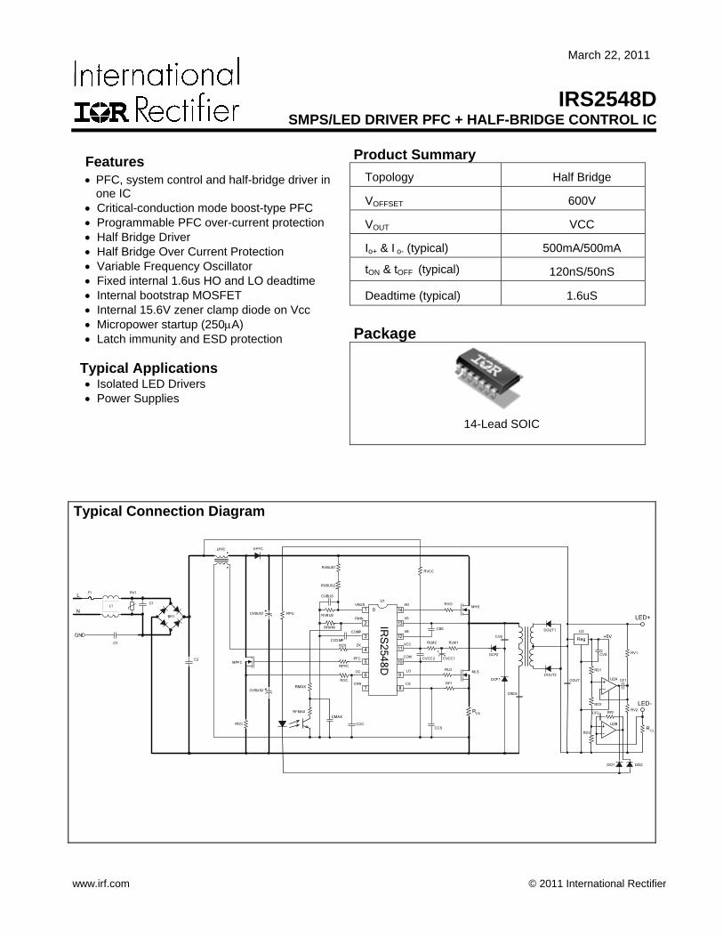
Typical Connection Diagram
RVBUS1
RLO
+
RVBUS2
C1
L
N
RV1F1
CVS
DCP2
DCP1
CCOMP
COCROC
MPFC
CVBUS2
CVBUS1
RPFC
RZX
CVBUS
RVBUS
RFMIN
RVCC
CCS
RCS
RF1
RLM1RLM2
RHOMHS
MLS
CBS
CVCC1CVCC
+
+BR1
C2
L1
CY
GND
DPFCLPFC
RFMAX
CRES
DOUT1
DOUT2
COUT
RPU
RCL
CVS
Reg+5V
LED+
LED-
RD1
RD2
RD3
RV1
RV2
CF1
CF2
2
ENN
1
2
3
VBUS
4
5
7
FMIN
6
7 8
13
12
11
10
9
14
OC
COMP
ZX
PFC
HO
VS
VB
VCC
COM
LO
CS
IRS
2548D
ROC
DO1 DO2
U1
U2A
U2B
U3
RF2
RMAX
CMAX
IRS2548D
www.irf.com © 2011 International Rectifier
2
Table of Contents Page
Description 3
Qualification Information 4
Absolute Maximum Ratings 5
Recommended Operating Conditions 6
Electrical Characteristics 6
Functional Block Diagram 9
State Diagram 10
Input/Output Pin Equivalent Circuit Diagram 11
Lead Definitions 12
Lead Assignments 12
Application Information and Additional Details 13
Package Details 19
Tape and Reel Details 20
Part Marking Information 21
Ordering Information 22

IRS2548D
www.irf.com © 2011 International Rectifier
3
Description The IRS2548D is a fully integrated, fully protected 600V LED or switched mode power supply control IC with integrated PFC control for a Boost pre-regulator. The IRS2548D is based on the popular IRS2168D electronic ballast control IC re-designed for use in LED driver or half-bridge power supply applications. The PFC circuitry operates in critical conduction mode and provides high PF, low THD and DC bus regulation. The IRS2548D features include programmable minimum run frequency and adjustable oscillator frequency that can be driven by an opto isolator or other feedback circuit in a feedback loop for frequency modulation in resonant systems. The IRS2548D also includes PFC over-voltage and over-current protection, half bridge over current protection and a logic level enable input that can be used for PWM dimming in LED drivers or general burst mode operation.
IRS2548D
www.irf.com © 2011 International Rectifier
4
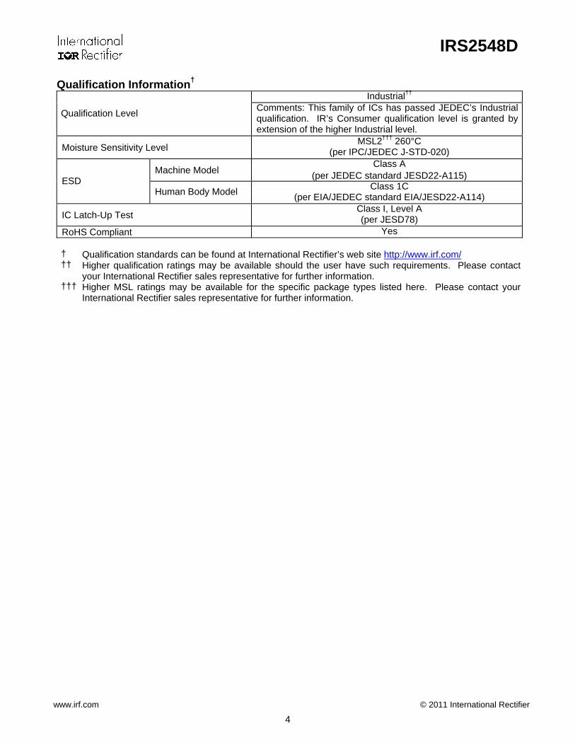
Qualification Information† Industrial††
Qualification Level Comments: This family of ICs has passed JEDEC’s Industrial qualification. IR’s Consumer qualification level is granted by extension of the higher Industrial level.
Moisture Sensitivity Level MSL2††† 260°C
(per IPC/JEDEC J-STD-020)
Machine Model Class A
(per JEDEC standard JESD22-A115) ESD Human Body Model Class 1C
(per EIA/JEDEC standard EIA/JESD22-A114)
IC Latch-Up Test Class I, Level A (per JESD78)
RoHS Compliant Yes
† Qualification standards can be found at International Rectifier’s web site http://www.irf.com/ †† Higher qualification ratings may be available should the user have such requirements. Please contact
your International Rectifier sales representative for further information. ††† Higher MSL ratings may be available for the specific package types listed here. Please contact your
International Rectifier sales representative for further information.
IRS2548D
www.irf.com © 2011 International Rectifier
5
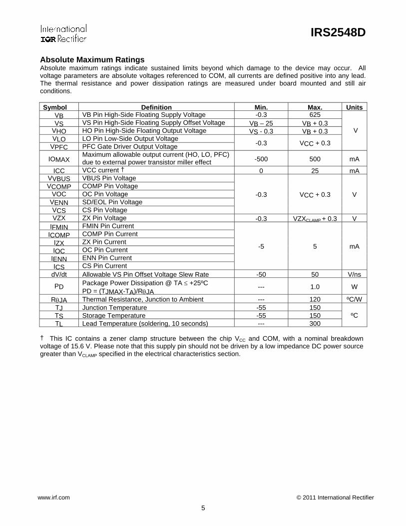
Absolute Maximum Ratings Absolute maximum ratings indicate sustained limits beyond which damage to the device may occur. All voltage parameters are absolute voltages referenced to COM, all currents are defined positive into any lead. The thermal resistance and power dissipation ratings are measured under board mounted and still air conditions. Symbol Definition Min. Max. Units
VB VB Pin High-Side Floating Supply Voltage -0.3 625 VS VS Pin High-Side Floating Supply Offset Voltage VB – 25 VB + 0.3
VHO HO Pin High-Side Floating Output Voltage VS - 0.3 VB + 0.3 VLO LO Pin Low-Side Output Voltage
VPFC PFC Gate Driver Output Voltage -0.3 VCC + 0.3
V
IOMAX Maximum allowable output current (HO, LO, PFC) due to external power transistor miller effect -500 500 mA
ICC VCC current † 0 25 mA VVBUS VBUS Pin Voltage VCOMP COMP Pin Voltage
VOC OC Pin Voltage VENN SD/EOL Pin Voltage VCS CS Pin Voltage
-0.3 VCC + 0.3 V
VZX ZX Pin Voltage -0.3 VZXCLAMP + 0.3 V IFMIN FMIN Pin Current
ICOMP COMP Pin Current IZX ZX Pin Current IOC OC Pin Current
IENN ENN Pin Current ICS CS Pin Current
-5 5 mA
dV/dt Allowable VS Pin Offset Voltage Slew Rate -50 50 V/ns
PD Package Power Dissipation @ TA ≤ +25ºC PD = (TJMAX-TA)/RθJA --- 1.0 W
RθJA Thermal Resistance, Junction to Ambient --- 120 ºC/W TJ Junction Temperature -55 150 TS Storage Temperature -55 150 TL Lead Temperature (soldering, 10 seconds) --- 300
ºC
† This IC contains a zener clamp structure between the chip VCC and COM, with a nominal breakdown voltage of 15.6 V. Please note that this supply pin should not be driven by a low impedance DC power source greater than VCLAMP specified in the electrical characteristics section.
IRS2548D
www.irf.com © 2011 International Rectifier
6
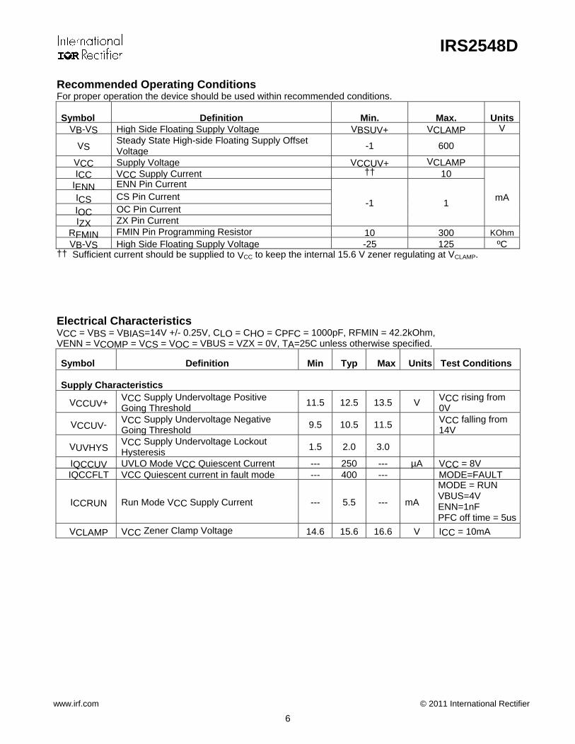
Recommended Operating Conditions For proper operation the device should be used within recommended conditions.
Symbol Definition Min. Max. Units VB-VS High Side Floating Supply Voltage VBSUV+ VCLAMP V
VS Steady State High-side Floating Supply Offset Voltage -1 600
VCC Supply Voltage VCCUV+ VCLAMP ICC VCC Supply Current †† 10 IENN ENN Pin Current ICS CS Pin Current IOC OC Pin Current IZX ZX Pin Current
-1 1 mA
RFMIN FMIN Pin Programming Resistor 10 300 KOhm VB-VS High Side Floating Supply Voltage -25 125 ºC
†† Sufficient current should be supplied to VCC to keep the internal 15.6 V zener regulating at VCLAMP.
Electrical Characteristics VCC = VBS = VBIAS=14V +/- 0.25V, CLO = CHO = CPFC = 1000pF, RFMIN = 42.2kOhm, VENN = VCOMP = VCS = VOC = VBUS = VZX = 0V, TA=25C unless otherwise specified.
Symbol Definition Min Typ Max Units Test Conditions
Supply Characteristics
VCCUV+ VCC Supply Undervoltage Positive Going Threshold 11.5 12.5 13.5 V VCC rising from
0V
VCCUV- VCC Supply Undervoltage Negative Going Threshold 9.5 10.5 11.5 VCC falling from
14V
VUVHYS VCC Supply Undervoltage Lockout Hysteresis 1.5 2.0 3.0
IQCCUV UVLO Mode VCC Quiescent Current --- 250 --- µA VCC = 8V IQCCFLT VCC Quiescent current in fault mode --- 400 --- MODE=FAULT
ICCRUN Run Mode VCC Supply Current --- 5.5 --- mA
MODE = RUN VBUS=4V ENN=1nF PFC off time = 5us
VCLAMP VCC Zener Clamp Voltage 14.6 15.6 16.6 V ICC = 10mA
IRS2548D
www.irf.com © 2011 International Rectifier
7
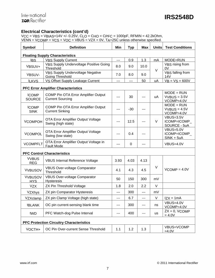
Electrical Characteristics (cont’d) VCC = VBS = VBIAS=14V +/- 0.25V, CLO = CHO = CPFC = 1000pF, RFMIN = 42.2kOhm, VENN = VCOMP = VCS = VOC = VBUS = VZX = 0V, TA=25C unless otherwise specified.
Symbol Definition Min Typ Max Units Test Conditions
Floating Supply Characteristics IBS VBS Supply Current --- 0.9 1.3 mA MODE=RUN
VBSUV+ VBS Supply Undervoltage Positive Going Threshold 8.0 9.0 10.0 VBS rising from
0V
VBSUV- VBS Supply Undervoltage Negative Going Threshold 7.0 8.0 9.0
V VBS falling from 14V
ILKVS VS Offset Supply Leakage Current --- --- 50 uA VB = VS = 600V
PFC Error Amplifier Characteristics
ICOMP SOURCE
COMP Pin OTA Error Amplifier Output Current Sourcing --- 30 --- uA
MODE = RUN VVBUS = 3.5V VCOMP=4.0V
ICOMP SINK
COMP Pin OTA Error Amplifier Output Current Sinking --- -30 ---
MODE = RUN VVBUS = 4.5V VCOMP=4.0V
VCOMPOH OTA Error Amplifier Output Voltage Swing (high state) --- 12.5 --- V
VBUS=3.5V ICOMP=ICOMP_SOURCE - 5uA
VCOMPOL OTA Error Amplifier Output Voltage Swing (low state) --- 0.4 ---
VBUS=5.0V ICOMP=ICOMP_SINK + 5uA
VCOMPFLT OTA Error Amplifier Output Voltage in Fault Mode --- 0 --- VBUS=4.0V
PFC Control Characteristics VVBUS
REG VBUS Internal Reference Voltage 3.93 4.03 4.13
VVBUSOV VBUS Over-voltage Comparator Threshold 4.1 4.3 4.5
V
VVBUSOV HYS
VBUS Over-voltage Comparator Hysteresis 50 150 300 mV
VCOMP = 4.0V
VZX ZX Pin Threshold Voltage 1.8 2.0 2.2 V
VZXhys ZX pin Comparator Hysteresis --- 300 --- mV
VZXclamp ZX pin Clamp Voltage (high state) --- 6.7 --- V IZX = 1mA
tBLANK OC pin current-sensing blank time --- 300 --- ns VBUS=4.0V VCOMP=4.0V
tWD PFC Watch-dog Pulse Interval --- 400 --- us ZX = 0, VCOMP = 4.0V
PFC Protection Circuitry Characteristics
VOCTH+ OC Pin Over-current Sense Threshold 1.1 1.2 1.3 VBUS=VCOMP =4.0V
IRS2548D
www.irf.com © 2011 International Rectifier
8
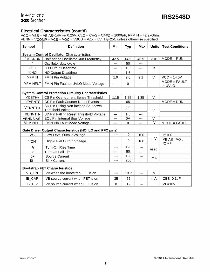
Electrical Characteristics (cont’d) VCC = VBS = VBIAS=14V +/- 0.25V, CLO = CHO = CPFC = 1000pF, RFMIN = 42.2kOhm, VENN = VCOMP = VCS = VOC = VBUS = VZX = 0V, TA=25C unless otherwise specified.
Symbol Definition Min Typ Max Units Test Conditions
System Control Oscillator Characteristics fOSCRUN Half-bridge Oscillator Run Frequency 42.5 44.5 46.5 kHz MODE = RUN
d Oscillator duty cycle --- 50 --- tdLO LO Output Deadtime --- 1.6 --- us tdHO HO Output Deadtime --- 1.6 ---
VFMIN FMIN Pin Voltage 1.9 2.0 2.1 V VCC = 14.0V
VFMINFLT FMIN Pin Fault or UVLO Mode Voltage --- 0 --- MODE = FAULT or UVLO
System Control Protection Circuitry Characteristics VCSTH+ CS Pin Over-current Sense Threshold 1.15 1.25 1.35 V
nEVENTS CS Pin Fault Counter No. of Events 65 MODE = RUN
VENNTH+ SD Pin Rising Non-latched Shutdown Threshold Voltage --- 2.0 ---
VENNTH- SD Pin Falling Reset Threshold Voltage --- 1.5 ---
V
VENNBIAS EOL Pin Internal Bias Voltage --- 0V --- V VFMINFLT FMIN Pin Fault Mode Voltage --- 0 --- V MODE = FAULT
Gate Driver Output Characteristics (HO, LO and PFC pins) VOL Low-Level Output Voltage --- 0 100 IO = 0
VOH High-Level Output Voltage --- 0 100 mV
VBIAS - VO , IO = 0
tr Turn-On Rise Time --- 120 --- tf Turn-Off Fall Time --- 50 ---
nsec
I0+ Source Current --- 180 --- I0- Sink Current --- 260 ---
mA
Bootstrap FET Characteristics VB_ON VB when the bootstrap FET is on --- 13.7 --- V
IB_CAP VB source current when FET is on 35 55 --- mA CBS=0.1uF IB_10V VB source current when FET is on 8 12 --- VB=10V
IRS2548D
www.irf.com © 2011 International Rectifier
9
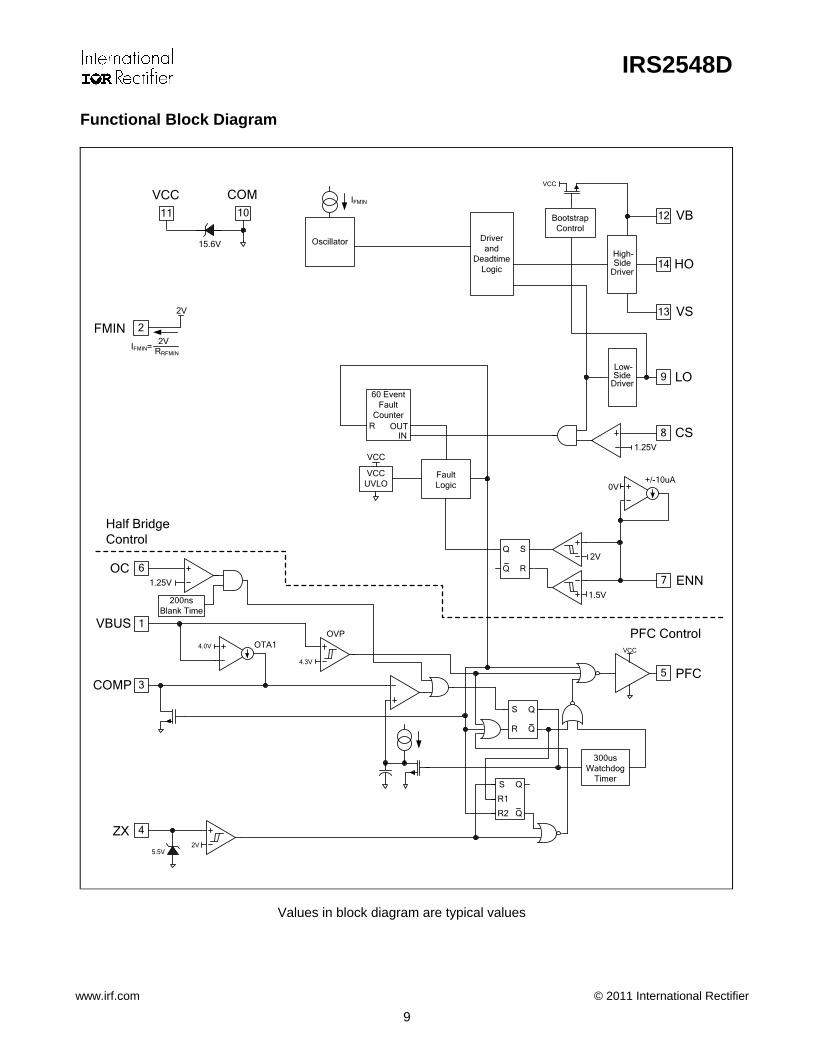
Functional Block Diagram
PFCCOMP
ZX
5.5V2V
QS
R2 Q
R1
QS
R Q
VCC
OC
VCC
FMIN
COM
VBUS
VB
HO
VS
LO
CS
High-Side
Driver
Low-Side
Driver
1.25V
8
11
6
2
1
12
14
13
9
53
4
VCCUVLO
300usWatchdog
Timer
10
OVP
4.3V
60 EventFault
Counter
4.0V OTA1
Driverand
DeadtimeLogic
15.6V
1.25V
BootstrapControl
VCC
200nsBlank Time
R
ENN7
0V
2V
1.5V
Half Bridge Control
PFC Control
INOUT
2V
2V
IFMIN
RRFMINIFMIN=
+/-10uAFaultLogic
Oscillator
VCC
Q S
RQ
Values in block diagram are typical values

IRS2548D
www.irf.com © 2011 International Rectifier
10
State Diagram
All values are typical. Please refer to application diagram on page 1.
IRS2548D
www.irf.com © 2011 International Rectifier
11
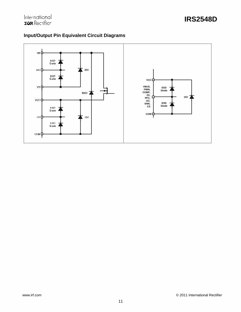
Input/Output Pin Equivalent Circuit Diagrams
VCC
COM
VBUS,FMIN,
COMP,ZX,
PFC,OC,
ENN,CS
ESD Diode
ESD Diode
15V
IRS2548D
www.irf.com © 2011 International Rectifier
12
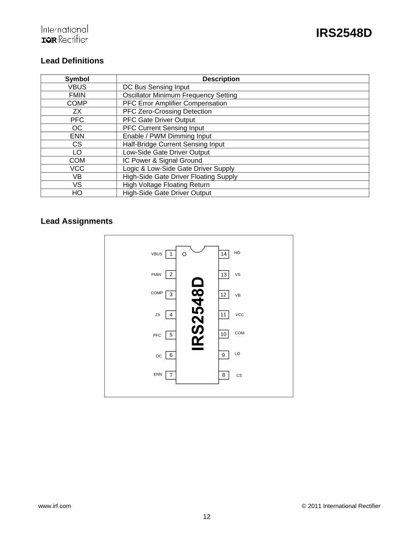
Lead Definitions
Symbol Description VBUS DC Bus Sensing Input FMIN Oscillator Minimum Frequency Setting
COMP PFC Error Amplifier Compensation ZX PFC Zero-Crossing Detection
PFC PFC Gate Driver Output OC PFC Current Sensing Input
ENN Enable / PWM Dimming Input CS Half-Bridge Current Sensing Input LO Low-Side Gate Driver Output
COM IC Power & Signal Ground VCC Logic & Low-Side Gate Driver Supply VB High-Side Gate Driver Floating Supply VS High Voltage Floating Return HO High-Side Gate Driver Output
Lead Assignments
13
12
11
10
9
COM
VCC
VB
VS
HO1
2
3
VBUS
4
5
7
COMP
FMIN
6
7
PFC
ZX
8ENN
LO
CS
14
OC
IRS2548D
www.irf.com © 2011 International Rectifier
13
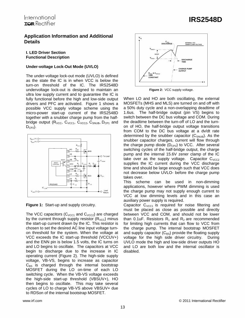
Application Information and Additional Details I. LED Driver Section Functional Description Under-voltage Lock-Out Mode (UVLO) The under-voltage lock-out mode (UVLO) is defined as the state the IC is in when VCC is below the turn-on threshold of the IC. The IRS2548D undervoltage lock-out is designed to maintain an ultra low supply current and to guarantee the IC is fully functional before the high and low-side output drivers and PFC are activated. Figure 1 shows a possible VCC supply voltage scheme using the micro-power start-up current of the IRS2548D together with a snubber charge pump from the half-bridge output (RVCC, CVCC1, CVCC2, CSNUB, DCP1 and DCP2).
IRS2548D
LO
COM
VB
VS
HO
VBUS (+)
V BUS (-)
VCC
CBS
14 MHS
C VCC2
RVCC
DCP1
DCP2
To Load
R CS
C SNUB
MLS
13
12
11
10
9
VRECT (+)
C VCC1
CS8
R3
C CS
IC COM
LoadReturn
R1R2
RLO
RHO
BSFETCONTROL
BSFET
Figure 1: Start-up and supply circuitry. The VCC capacitors (CVCC1 and CVCC2) are charged by the current through supply resistor (RVCC) minus the start-up current drawn by the IC. This resistor is chosen to set the desired AC line input voltage turn-on threshold for the system. When the voltage at VCC exceeds the IC start-up threshold (VCCUV+) and the ENN pin is below 1.5 volts, the IC turns on and LO begins to oscillate. The capacitors at VCC begin to discharge due to the increase in IC operating current (Figure 2). The high-side supply voltage, VB-VS, begins to increase as capacitor CBS is charged through the internal bootstrap MOSFET during the LO on-time of each LO switching cycle. When the VB-VS voltage exceeds the high-side start-up threshold (VBSUV+), HO then begins to oscillate. This may take several cycles of LO to charge VB-VS above VBSUV+ due to RDSon of the internal bootstrap MOSFET.
DISCHARGETIME
INTERNAL VCCZENER CLAMP VOLTAGE
VHYST
VUVLO+
VUVLO-
CHARGE PUMPOUTPUT
t
VC1
RVCC & CVCC1,2TIMECONSTANT
CVCCDISCHARGE
Figure 2: VCC supply voltage. When LO and HO are both oscillating, the external MOSFETs (MHS and MLS) are turned on and off with a 50% duty cycle and a non-overlapping deadtime of 1.6us. The half-bridge output (pin VS) begins to switch between the DC bus voltage and COM. During the deadtime between the turn-off of LO and the turn-on of HO, the half-bridge output voltage transitions from COM to the DC bus voltage at a dv/dt rate determined by the snubber capacitor (CSNUB). As the snubber capacitor charges, current will flow through the charge pump diode (DCP2) to VCC. After several switching cycles of the half-bridge output, the charge pump and the internal 15.6V zener clamp of the IC take over as the supply voltage. Capacitor CVCC2 supplies the IC current during the VCC discharge time and should be large enough such that VCC does not decrease below UVLO- before the charge pump takes over. This scheme can be used in non-dimming applications, however where PWM dimming is used the charge pump may not supply enough current to VCC at low dimming levels and in this case an auxiliary power supply is required. Capacitor CVCC1 is required for noise filtering and must be placed as close as possible and directly between VCC and COM, and should not be lower than 0.1uF. Resistors R1 and R2 are recommended for limiting high currents that can flow to VCC from the charge pump. The internal bootstrap MOSFET and supply capacitor (CBS) provide the floating supply voltage for the high side driver circuitry. During UVLO mode the high and low-side driver outputs HO and LO are both low and the internal oscillator is disabled.
IRS2548D
www.irf.com © 2011 International Rectifier
14
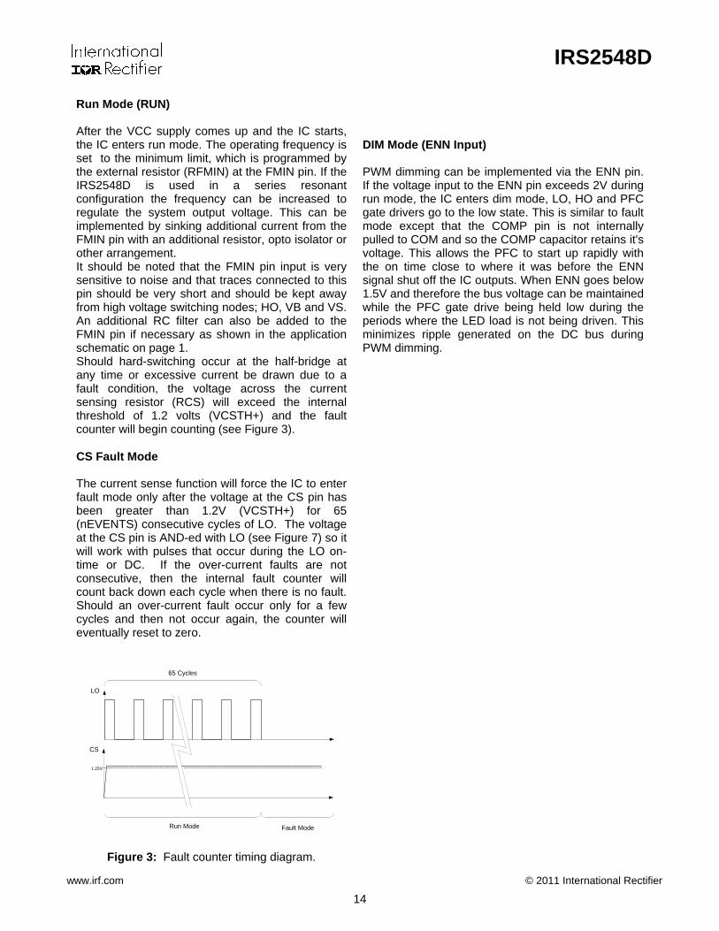
Run Mode (RUN) After the VCC supply comes up and the IC starts, the IC enters run mode. The operating frequency is set to the minimum limit, which is programmed by the external resistor (RFMIN) at the FMIN pin. If the IRS2548D is used in a series resonant configuration the frequency can be increased to regulate the system output voltage. This can be implemented by sinking additional current from the FMIN pin with an additional resistor, opto isolator or other arrangement. It should be noted that the FMIN pin input is very sensitive to noise and that traces connected to this pin should be very short and should be kept away from high voltage switching nodes; HO, VB and VS. An additional RC filter can also be added to the FMIN pin if necessary as shown in the application schematic on page 1. Should hard-switching occur at the half-bridge at any time or excessive current be drawn due to a fault condition, the voltage across the current sensing resistor (RCS) will exceed the internal threshold of 1.2 volts (VCSTH+) and the fault counter will begin counting (see Figure 3). CS Fault Mode The current sense function will force the IC to enter fault mode only after the voltage at the CS pin has been greater than 1.2V (VCSTH+) for 65 (nEVENTS) consecutive cycles of LO. The voltage at the CS pin is AND-ed with LO (see Figure 7) so it will work with pulses that occur during the LO on-time or DC. If the over-current faults are not consecutive, then the internal fault counter will count back down each cycle when there is no fault. Should an over-current fault occur only for a few cycles and then not occur again, the counter will eventually reset to zero.
LO
CS
65 Cycles
Run Mode Fault Mode
1.25V
Figure 3: Fault counter timing diagram.
DIM Mode (ENN Input) PWM dimming can be implemented via the ENN pin. If the voltage input to the ENN pin exceeds 2V during run mode, the IC enters dim mode, LO, HO and PFC gate drivers go to the low state. This is similar to fault mode except that the COMP pin is not internally pulled to COM and so the COMP capacitor retains it's voltage. This allows the PFC to start up rapidly with the on time close to where it was before the ENN signal shut off the IC outputs. When ENN goes below 1.5V and therefore the bus voltage can be maintained while the PFC gate drive being held low during the periods where the LED load is not being driven. This minimizes ripple generated on the DC bus during PWM dimming.
IRS2548D
www.irf.com © 2011 International Rectifier
15
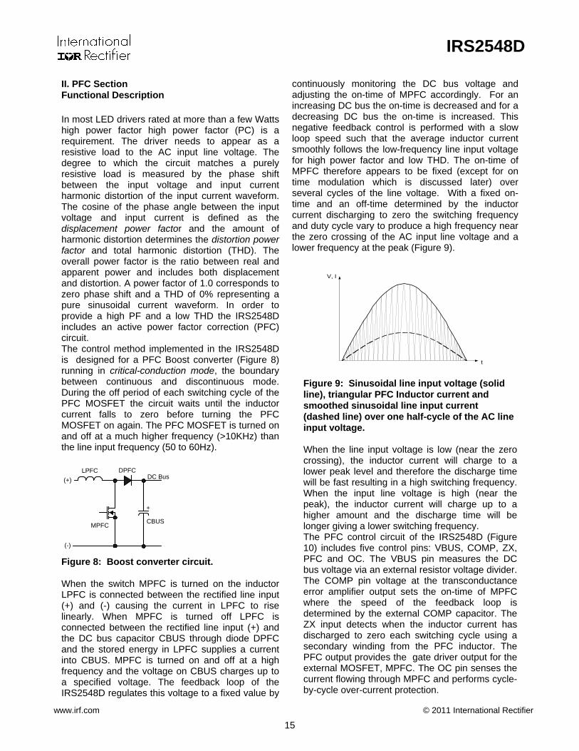
II. PFC Section Functional Description In most LED drivers rated at more than a few Watts high power factor high power factor (PC) is a requirement. The driver needs to appear as a resistive load to the AC input line voltage. The degree to which the circuit matches a purely resistive load is measured by the phase shift between the input voltage and input current harmonic distortion of the input current waveform. The cosine of the phase angle between the input voltage and input current is defined as the displacement power factor and the amount of harmonic distortion determines the distortion power factor and total harmonic distortion (THD). The overall power factor is the ratio between real and apparent power and includes both displacement and distortion. A power factor of 1.0 corresponds to zero phase shift and a THD of 0% representing a pure sinusoidal current waveform. In order to provide a high PF and a low THD the IRS2548D includes an active power factor correction (PFC) circuit. The control method implemented in the IRS2548D is designed for a PFC Boost converter (Figure 8) running in critical-conduction mode, the boundary between continuous and discontinuous mode. During the off period of each switching cycle of the PFC MOSFET the circuit waits until the inductor current falls to zero before turning the PFC MOSFET on again. The PFC MOSFET is turned on and off at a much higher frequency (>10KHz) than the line input frequency (50 to 60Hz).
CBUS
+
(+)
(-)
MPFC
LPFC DPFCDC Bus
Figure 8: Boost converter circuit. When the switch MPFC is turned on the inductor LPFC is connected between the rectified line input (+) and (-) causing the current in LPFC to rise linearly. When MPFC is turned off LPFC is connected between the rectified line input (+) and the DC bus capacitor CBUS through diode DPFC and the stored energy in LPFC supplies a current into CBUS. MPFC is turned on and off at a high frequency and the voltage on CBUS charges up to a specified voltage. The feedback loop of the IRS2548D regulates this voltage to a fixed value by
continuously monitoring the DC bus voltage and adjusting the on-time of MPFC accordingly. For an increasing DC bus the on-time is decreased and for a decreasing DC bus the on-time is increased. This negative feedback control is performed with a slow loop speed such that the average inductor current smoothly follows the low-frequency line input voltage for high power factor and low THD. The on-time of MPFC therefore appears to be fixed (except for on time modulation which is discussed later) over several cycles of the line voltage. With a fixed on-time and an off-time determined by the inductor current discharging to zero the switching frequency and duty cycle vary to produce a high frequency near the zero crossing of the AC input line voltage and a lower frequency at the peak (Figure 9).
V, I
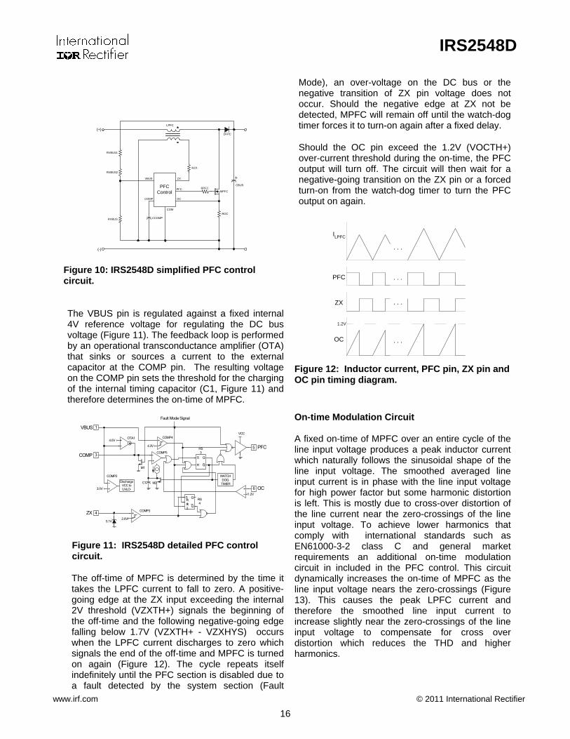
t Figure 9: Sinusoidal line input voltage (solid line), triangular PFC Inductor current and smoothed sinusoidal line input current (dashed line) over one half-cycle of the AC line input voltage. When the line input voltage is low (near the zero crossing), the inductor current will charge to a lower peak level and therefore the discharge time will be fast resulting in a high switching frequency. When the input line voltage is high (near the peak), the inductor current will charge up to a higher amount and the discharge time will be longer giving a lower switching frequency. The PFC control circuit of the IRS2548D (Figure 10) includes five control pins: VBUS, COMP, ZX, PFC and OC. The VBUS pin measures the DC bus voltage via an external resistor voltage divider. The COMP pin voltage at the transconductance error amplifier output sets the on-time of MPFC where the speed of the feedback loop is determined by the external COMP capacitor. The ZX input detects when the inductor current has discharged to zero each switching cycle using a secondary winding from the PFC inductor. The PFC output provides the gate driver output for the external MOSFET, MPFC. The OC pin senses the current flowing through MPFC and performs cycle-by-cycle over-current protection.
IRS2548D
www.irf.com © 2011 International Rectifier
16
RVBUS1
RVBUS2
RVBUS CCOMP
LPFC
MPFCRPFC
DFPC
CBUS
(+)
(-)
RZX
PFCControl
VBUS
COMP
PFC
ZX
COM
OC
ROC
Figure 10: IRS2548D simplified PFC control circuit.
The VBUS pin is regulated against a fixed internal 4V reference voltage for regulating the DC bus voltage (Figure 11). The feedback loop is performed by an operational transconductance amplifier (OTA) that sinks or sources a current to the external capacitor at the COMP pin. The resulting voltage on the COMP pin sets the threshold for the charging of the internal timing capacitor (C1, Figure 11) and therefore determines the on-time of MPFC.
4
3
1
QS
R Q
2.0V
VBUS
COMP
ZX
5.1V
4.0VOTA1
4.3V 5 PFC
QS
R2
Q
R1
COMP3
COMP4
COMP5RS3
RS4
VCC
Fault Mode Signal
M1
WATCHDOGTIMERM2C1
3.0V
DischargeVCC toUVLO-
COMP2
6 OC1.2V
Figure 11: IRS2548D detailed PFC control circuit.
The off-time of MPFC is determined by the time it takes the LPFC current to fall to zero. A positive-going edge at the ZX input exceeding the internal 2V threshold (VZXTH+) signals the beginning of the off-time and the following negative-going edge falling below 1.7V (VZXTH+ - VZXHYS) occurs when the LPFC current discharges to zero which signals the end of the off-time and MPFC is turned on again (Figure 12). The cycle repeats itself indefinitely until the PFC section is disabled due to a fault detected by the system section (Fault
Mode), an over-voltage on the DC bus or the negative transition of ZX pin voltage does not occur. Should the negative edge at ZX not be detected, MPFC will remain off until the watch-dog timer forces it to turn-on again after a fixed delay.
Should the OC pin exceed the 1.2V (VOCTH+) over-current threshold during the on-time, the PFC output will turn off. The circuit will then wait for a negative-going transition on the ZX pin or a forced turn-on from the watch-dog timer to turn the PFC output on again.
ILPFC
PFC
ZX
OC
1.2V
. . .
. . .
. . .
. . .
Figure 12: Inductor current, PFC pin, ZX pin and OC pin timing diagram.
On-time Modulation Circuit
A fixed on-time of MPFC over an entire cycle of the line input voltage produces a peak inductor current which naturally follows the sinusoidal shape of the line input voltage. The smoothed averaged line input current is in phase with the line input voltage for high power factor but some harmonic distortion is left. This is mostly due to cross-over distortion of the line current near the zero-crossings of the line input voltage. To achieve lower harmonics that comply with international standards such as EN61000-3-2 class C and general market requirements an additional on-time modulation circuit in included in the PFC control. This circuit dynamically increases the on-time of MPFC as the line input voltage nears the zero-crossings (Figure 13). This causes the peak LPFC current and therefore the smoothed line input current to increase slightly near the zero-crossings of the line input voltage to compensate for cross over distortion which reduces the THD and higher harmonics.
IRS2548D
www.irf.com © 2011 International Rectifier
17
0
0
ILPFC
PFCpin
near peak region ofrectified AC line
near zero-crossing regionof rectified AC line
Figure 13: On-time modulation circuit timing diagram
DC Bus Over-voltage Protection
Should over-voltage occur on the DC bus and the VBUS pin exceeds the internal 4.3V threshold (VBUSOV+), the PFC output is disabled (set to a logic ‘low’). When the DC bus decreases again and the VBUS pin decreases below the internal 4.15V threshold (VBUSOV-), a watch-dog pulse is forced on the PFC pin and normal PFC operation is resumed.
III. Design Equations (Half-Bridge)
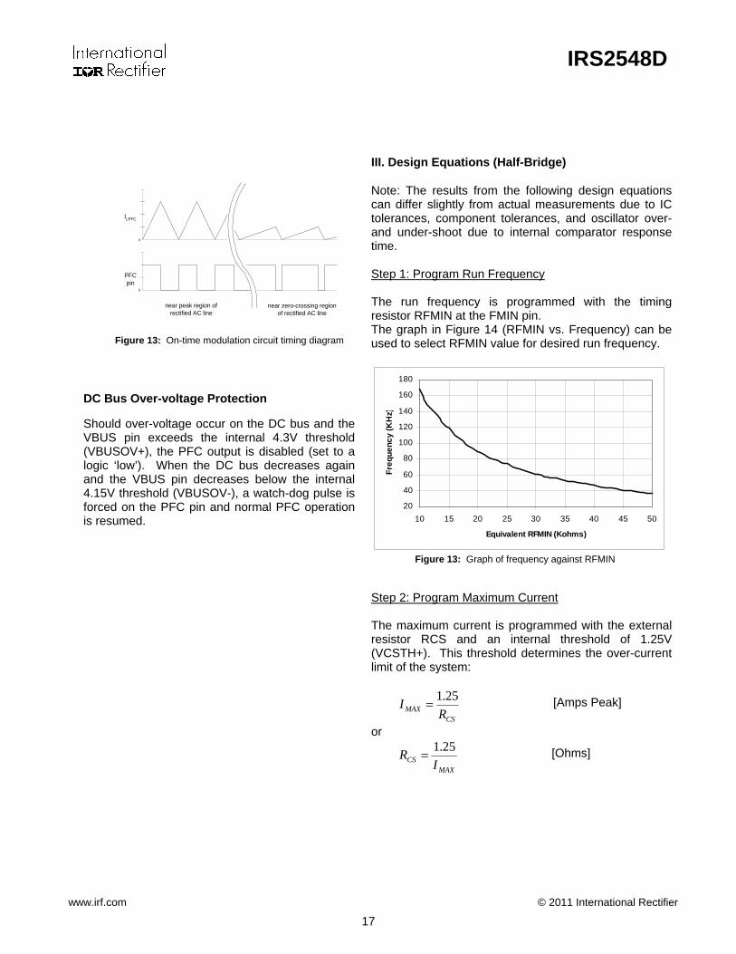
Note: The results from the following design equations can differ slightly from actual measurements due to IC tolerances, component tolerances, and oscillator over- and under-shoot due to internal comparator response time. Step 1: Program Run Frequency The run frequency is programmed with the timing resistor RFMIN at the FMIN pin. The graph in Figure 14 (RFMIN vs. Frequency) can be used to select RFMIN value for desired run frequency.
20
40
60
80
100
120
140
160
180
10 15 20 25 30 35 40 45 50
Equivalent RFMIN (Kohms)
Freq
uenc
y (K
Hz)
Figure 13: Graph of frequency against RFMIN
Step 2: Program Maximum Current The maximum current is programmed with the external resistor RCS and an internal threshold of 1.25V (VCSTH+). This threshold determines the over-current limit of the system:
CSMAX R
I 25.1= [Amps Peak]
or
MAXCS I
R 25.1= [Ohms]
IRS2548D
www.irf.com © 2011 International Rectifier
18
IV. PFC Design Equations
Step1: Calculate PFC inductor value:
VBUSPfVACVACVBUSL
OUTMIN
MINMINPFC ⋅⋅⋅
⋅⋅⋅−=
2)2( 2 η [Henries]
where, VBUS = DC bus voltage
MINVAC = Minimum rms AC input voltage η = PFC efficiency (typically 0.95)
MINf = Minimum PFC switching frequency at minimum AC input voltage
OUTP = System output power The following simplified formula may be also used. This formula has been empirically determined based on lowest THD results measured from test circuits. It is not derived mathematically from the formula above.
VBUSPfVACVACVBUSeL
OUTMIN
MINMINPFC
⋅⋅⋅⋅⋅⋅⋅−⋅−
=22
)2()68( η [Henries]
Step 2: Calculate peak PFC inductor current:
η⋅
⋅⋅=
MIN
OUTPK VAC
Pi
22 [Amps Peak]
Note: The PFC inductor must not saturate at PKi over the specified system operating temperature range. Proper core sizing and air-gapping should be considered in the inductor design.
Step 3: Calculate PFC over-current resistor ROC value:
PK
OC iR 25.1
= where VCSTH+ = 1.25V [Ohms]
IRS2548D
www.irf.com © 2011 International Rectifier
19
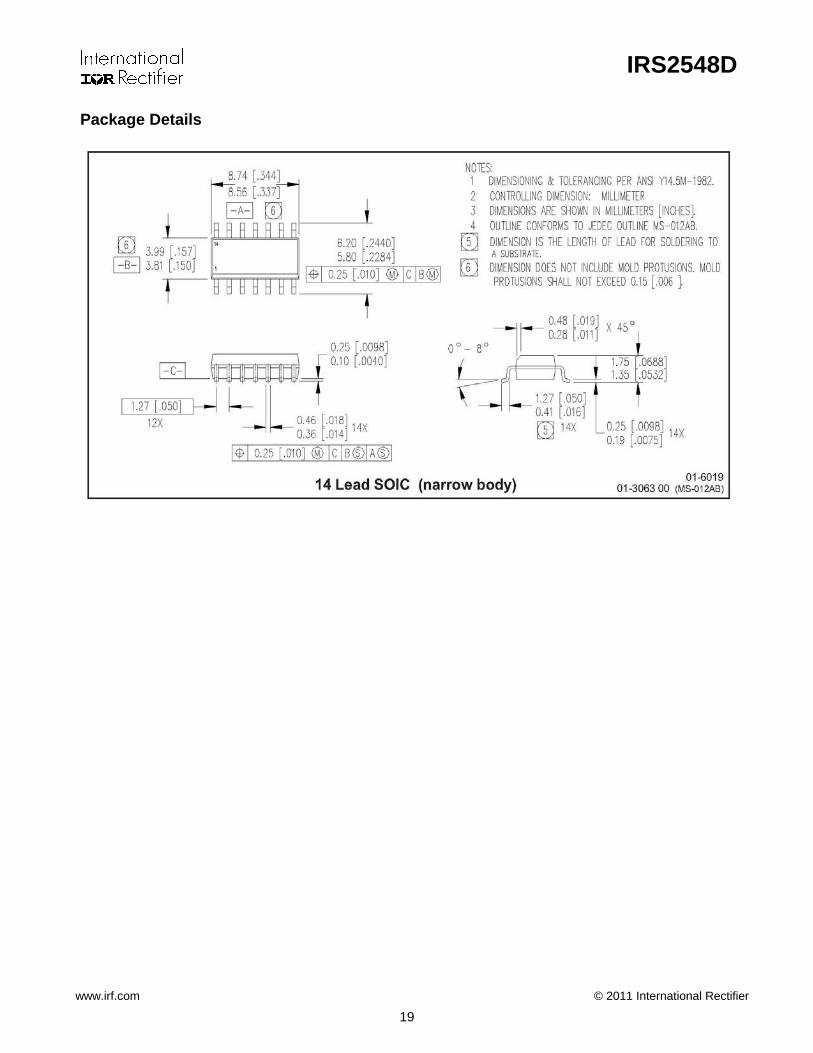
Package Details
IRS2548D
www.irf.com © 2011 International Rectifier
20
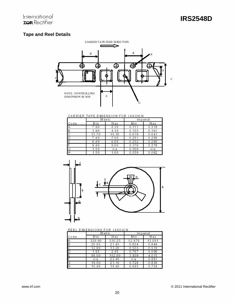
Tape and Reel Details
IRS2548D
www.irf.com © 2011 International Rectifier
21
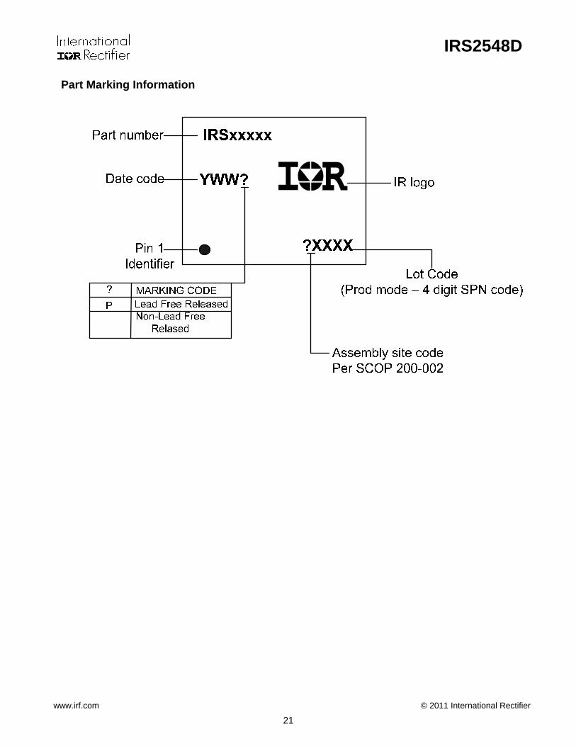
Part Marking Information
IRS2548D
www.irf.com © 2011 International Rectifier
22
Ordering Information
Standard Pack Base Part Number Package Type
Form Quantity Complete Part Number
Tube/Bulk 55 IRS2548DSPBF IRS2548D SOIC14N
Tape and Reel 2500 IRS2548DSTRPBF
The information provided in this document is believed to be accurate and reliable. However, International Rectifier assumes no
responsibility for the consequences of the use of this information. International Rectifier assumes no responsibility for any infringement of patents or of other rights of third parties which may result from the use of this information. No license is granted by implication or otherwise under any patent or patent rights of International Rectifier. The specifications mentioned in this document are subject to
change without notice. This document supersedes and replaces all information previously supplied.
For technical support, please contact IR’s Technical Assistance Center http://www.irf.com/technical-info/
WORLD HEADQUARTERS:
233 Kansas St., El Segundo, California 90245 Tel: (310) 252-7105


![TFT-DISPLAY D - HY-LINE · 4.1 Absolute Ratings ofTFT LCD Module 4.2 Absolute Ratings of Environment Item Symbol Min. Max. Unit Operating Temperature TOP 0 +60 [oC] Operation Humidity](https://img.dokumen.tips/doc/110x75/5f0f9b1f7e708231d444fee5/tft-display-d-hy-line-41-absolute-ratings-oftft-lcd-module-42-absolute-ratings.jpg)